

Page 1

Global LCD Panel Exchange Center
www.panelook.com
©Copyright AU Optronics, Inc.
Feb, 2009 All Rights Reserved. T370HW03 V2 1/32
No Reproduction and Redistribution Allowed
One step solution for LCD / PDP / OLED panel application: Datasheet, inventory and accessory!
www.panelook.com
Page 2

Global LCD Panel Exchange Center
www.panelook.com
Update date: 2009/5/21
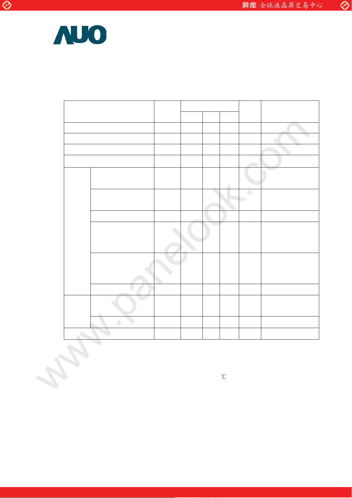
Product Specifications
37” HDTV Color TFT-LCD Module
Model Name: T370HW03. V2
() Preliminary Specifications
(*) Final Specifications
©Copyright AU Optronics, Inc.
June, 2008 All Rights Reserved. T370HW03 V2 2/31
No Reproduction and Redistribution Allowed
One step solution for LCD / PDP / OLED panel application: Datasheet, inventory and accessory!
www.panelook.com
Page 3
Global LCD Panel Exchange Center
www.panelook.com
Contents
No
COVER
CONTENTS
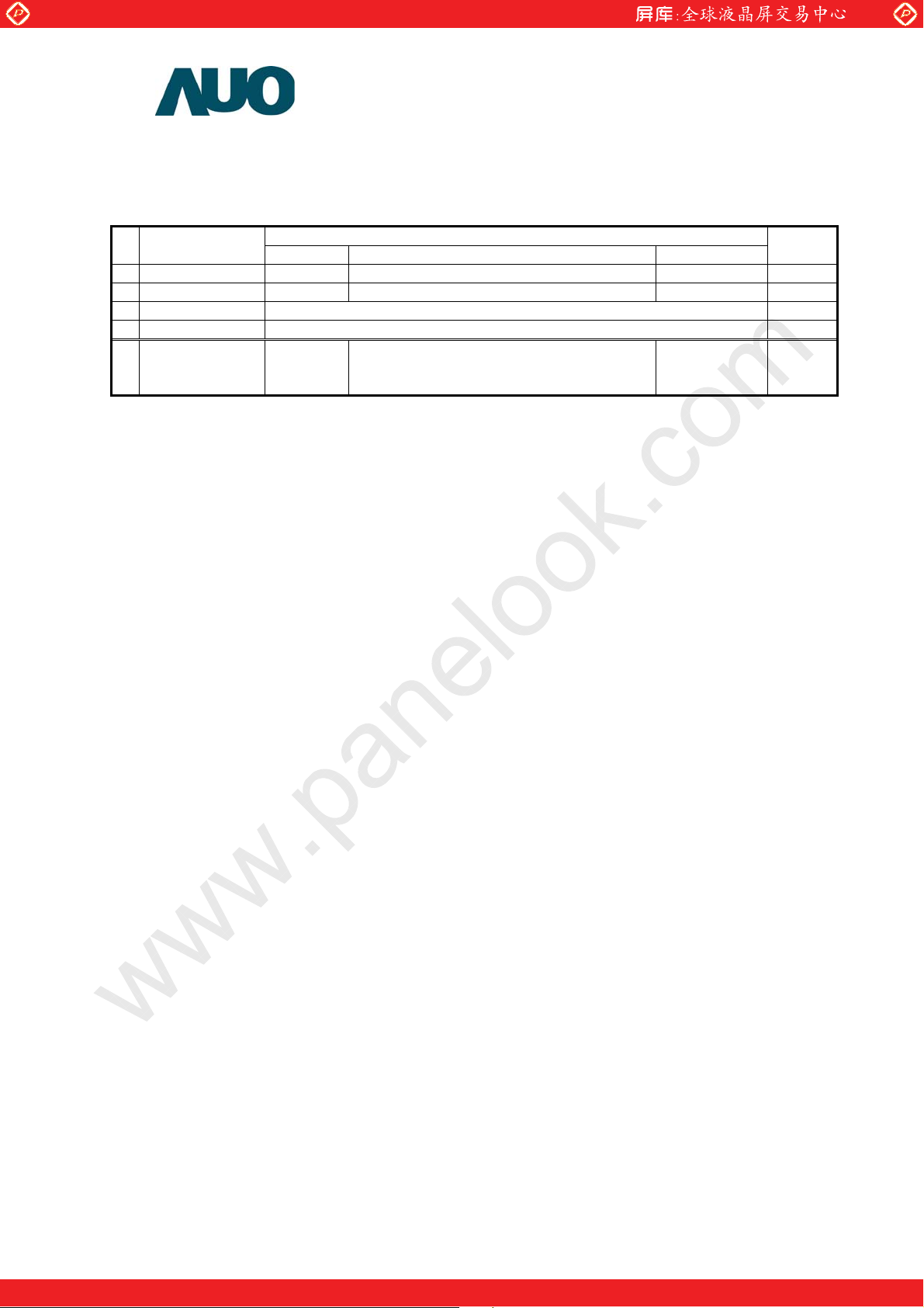
RECORD OF REVISIONS
1 GENERAL DESCRIPTION
2 ABSOLUTE MAXIMUM RATINGS
3 ELECTRICAL SPECIFICATIONS
3-1 ELECTRICAL CHARACTREISTIC
3-2 INTERFACE CONNECTIONS
3-3 SIGNAL TIMING SPECIFICATIONS
3-4 SIGNAL TIMING WAVEFORMS
3-5 COLOR INPUT DATA REFERENCE
3-6 POWER SEQUENCE
4 OPTICAL CHARACTERISTICS
5 MECHANICAL CHARACTERISTICS
6 RELIABLITY
7 INTERNATIONAL STANDARDS
7-1 SAFETY
7-2 EMC
8 PACKING
9 PRECAUTIONS
©Copyright AU Optronics, Inc.
June, 2008 All Rights Reserved. T370HW03 V2 3/31
No Reproduction and Redistribution Allowed
One step solution for LCD / PDP / OLED panel application: Datasheet, inventory and accessory!
www.panelook.com
Page 4
Global LCD Panel Exchange Center
Record of Revision
Version Date No Old Description New Description Remark
0 2009.3.24 First draft
1 2009,04,23 Update cycle to cycle jitter
2 2009,05,14
www.panelook.com
Update 25
кʳ ˩
3 2009,05,21
Update packing information
©Copyright AU Optronics, Inc.
June, 2008 All Rights Reserved. T370HW03 V2 4/31
No Reproduction and Redistribution Allowed
One step solution for LCD / PDP / OLED panel application: Datasheet, inventory and accessory!
www.panelook.com
Page 5
Global LCD Panel Exchange Center
1. General Description
This specification applies to the 37.0 inch Color TFT-LCD Module T370HW03 V2. This
LCD module has a TFT active matrix type liquid crystal panel 1920x1080 pixels, and
diagonal size of 37.0 inch. This module supports 1920x1080 HDTV mode (Non-interlace).
Each pixel is divided into Red, Green and Blue sub-pixels or dots which are arranged in
vertical stripes. Gray scale or the brightness of the sub-pixel color is determined with a 10-bit
gray scale signal for each dot.
This model use 2008 Front Mount Bezel structure with narrow bezel design.
The T370HW03 V2 has been designed to apply the 8-bit+FRC 4 channel LVDS interface
method. It is intended to support displays where high brightness, wide viewing angle, high
www.panelook.com
color saturation, and high color depth are very important.
The T370HW03 V2 model is RoHS verified which can be distinguished on panel label.
*
General Information
Items Specification Unit Note
Active Screen Size 37.01 inch
Display Area 819.36 (H) x 460.89(V) mm
Outline Dimension 855.8(H)×497.4(V)×44.9(D) mm
Driver Element a-Si TFT active matrix
Display Colors 8 bit +FRC,1.074B Colors
Number of Pixels 1920 x 1080 Pixel
Pixel Pitch 0.42675(H) x 0.42675(W) mm
Pixel Arrangement RGB vertical stripe
Display Operation Mode Normally Black
Surface Treatment AG Haze= 11%, 3H
Weight 9,000(Max) g
Lamp quantity, type 16, Straight type Pcs
©Copyright AU Optronics, Inc.
June, 2008 All Rights Reserved. T370HW03 V2 5/31
No Reproduction and Redistribution Allowed
One step solution for LCD / PDP / OLED panel application: Datasheet, inventory and accessory!
www.panelook.com
Page 6
Global LCD Panel Exchange Center
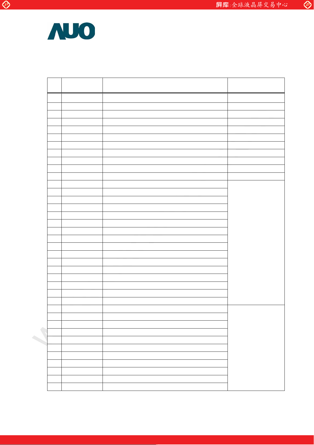
2. Absolute Maximum Ratings
The following are maximum values that, if exceeded, may cause permanent damage to the device.
Item Symbol Min Max Unit Note
Logic/LCD Drive Voltage Vcc -0.3 14 [Volt] [1]
Input Voltage of Signal Vin -0.3 4 [Volt] [1]
Operating Temperature TOP 0 50 [oC] [2]
Operating Humidity HOP 10 90 [%RH] [2]
Storage Temperature TST -20 60 [oC] [2]
Storage Humidity HST 10 90 [%RH] [2]
www.panelook.com
Panel surface temperature PST 65 [oC]
Note 1: Duration = 50msec
Note 2 : Maximum Wet-Bulb should be 39 and No condensation.
The relative humidity must not exceed 90% non-condensing at temperatures of 40 or less. At temperatures
greater than 40 , the wet bulb temperature must not exceed 39 .
кк
к
к
©Copyright AU Optronics, Inc.
June, 2008 All Rights Reserved. T370HW03 V2 6/31
No Reproduction and Redistribution Allowed
One step solution for LCD / PDP / OLED panel application: Datasheet, inventory and accessory!
www.panelook.com
Page 7
Global LCD Panel Exchange Center
D
3. Electrical Characteristics
The T370HW03 V2 requires two power inputs. One is employed to power the LCD electronics and to drive the
TFT array and liquid crystal. The second input power for the BLU, is to power lamps.
3-1 Electrical Characteristics (Ta=25±±±±2oC)
www.panelook.com
Values Parameter Symbol
Unit Notes
Min Typ Max
Power Supply Input Voltage Vcc 10.8 12.0 13.2 Vdc
Power Supply Input Current Icc 1
1.2 A [1]
Power Consumption Pc - 12 14.4 Watt [1]
LV DS
Interface
Inrush Current I
ifferential Input High
Threshold Voltage
Differential Input Low
Threshold Voltage
Common Input Voltage
- 4 Apeak [2]
RUSH
VTH 100 mV [3]
V
-100 mV [3]
TL
V
1.0 1.2 1.4 V
ICM
LVDS Clock to Data
Skew Margin
t
-0.4 - +0.4 ns
RMG
LVDS Clock to Clock
Skew Margin(Cycle to
Cycle jitter)
t
-2% - +2% Tclk
RCL
[7]
66MHz Fclk
80MHz
[8]
66MHz Fclk
80MHz
Interface
Life Time
Differential input voltage
Input High Threshold Voltage
Input Low Threshold Voltage
|
V
ID
V
IH
(High)
VIL (Low) 0 0.9 Vdc
50000 Hours
100 400 600 mV
|
2.4 3.3 Vdc CMOS
Note :
1. The check pattern is base on white pattern. The ripple voltage should be controlled under 10% of V
=vf
Vcc=12.0V,
120Hz, fCLK=75Mhz for one channel, 25 , Test Pattern : White Patternк
©Copyright AU Optronics, Inc.
June, 2008 All Rights Reserved. T370HW03 V2 7/31
No Reproduction and Redistribution Allowed
CC
One step solution for LCD / PDP / OLED panel application: Datasheet, inventory and accessory!
www.panelook.com
Page 8

Global LCD Panel Exchange Center
www.panelook.com
2. Measurement condition :
10%
GND
Figure 1: Measurement of I
3. Measurement of LVDS differential voltage is shown in Figure 2.
VTH
VCIM
VTL
100%
90%
T
rush
= 470ȝs
rush
0V
Figure 2 : LVDS Differential Voltage
4. The performance of the Lamp in LCM, for example life time or brightness, is extremely influenced by
the characteristics of the DC-AC Inverter. So all the parameters of an inverter should be carefully
designed so as not to produce too much leakage current from high-voltage output of the inverter.
When you design or order the inverter, please make sure unwanted lighting caused by the mismatch
of the lamp and the inverter (no lighting, flicker, etc) never occurs. When you confirm it, the LCD
Assembly should be operated in the same condition as installed in your instrument.
5. Do not attach a conducting tape to lamp connecting wire. If the lamp wire attach to conducting tape,
TFT-LCD Module have a low luminance and the inverter has abnormal action because leakage current
occurs between lamp wire and conducting tape.
6. The relative humidity must not exceed 90% non-condensing at temperatures of 40 or less. At
temperatures greater than 40 , the wet bulb temperature must not exceed 39 . When operate at low
temperatures, the brightness of CCFL will drop and the life time of CCFL will be reduced.
7. Measurement of LVDS Clock to Data Skew Margin is shown in Figure 3.
кк
к
©Copyright AU Optronics, Inc.
June, 2008 All Rights Reserved. T370HW03 V2 8/31
No Reproduction and Redistribution Allowed
One step solution for LCD / PDP / OLED panel application: Datasheet, inventory and accessory!
www.panelook.com
Page 9

Global LCD Panel Exchange Center
www.panelook.com
8. Measurement of LVDS Clock to Clock Skew Margin is shown in Figure 4.
Figure 3: LVDS Clock to Data Skew Margin
Figure 4: LVDS Clock to Clock Skew Margin
©Copyright AU Optronics, Inc.
June, 2008 All Rights Reserved. T370HW03 V2 9/31
No Reproduction and Redistribution Allowed
One step solution for LCD / PDP / OLED panel application: Datasheet, inventory and accessory!
www.panelook.com
Page 10
Global LCD Panel Exchange Center
3-2 Interface Connections
LCD connector : JAE FI-RE51S-HF
Pin
No
Symbol Description Note
1 Reserve AUO internal use ʳ
2 Reserve AUO internal use ʳ
3 Reserve AUO internal use ʳ
4 Reserve AUO internal use ʳ
5 Reserve AUO internal use ʳ
6 Reserve AUO internal use ʳ
7 LVDS Option Low/Open for Normal (NS), High for JEIDA Default : NS mode
8 Reserve AUO internal use ʳ
9 Reserve AUO internal use ʳ
10 Reserve AUO internal use ʳ
11 GND Ground ʳ
12 R1_0- LVDS Channel 1, Signal 013 R1_0+ LVDS Channel 1, Signal 0+
14 R1_1- LVDS Channel 1, Signal 115 R1_1+ LVDS Channel 1, Signal 1+
16 R1_2- LVDS Channel 1, Signal 217 R1_2+ LVDS Channel 1, Signal 2+
18 GND Ground
19 R1_CLK- LVDS Channel 1, Clock 20 R1_CLK+ LVDS Channel 1, Clock +
21 GND Ground
22 R1_3- LVDS Channel 1, Signal 323 R1_3+ LVDS Channel 1, Signal 3+
24 R1_4- LVDS Channel 1, Signal 425 R1_4+ LVDS Channel 1, Signal 4+
26 GND Ground
27 GND Ground
28 R2_0- LVDS Channel 2, Signal 029 R2_0+ LVDS Channel 2, Signal 0+
30 R2_1- LVDS Channel 2, Signal 131 R2_1+ LVDS Channel 2, Signal 1+
32 R2_2- LVDS Channel 2, Signal 233 R2_2+ LVDS Channel 2, Signal 2+
34 GND Ground
35 R2_CLK- LVDS Channel 2, Clock 36 R2_CLK+ LVDS Channel 2, Clock +
37 GND Ground
38 R2_3- LVDS Channel 2, Signal 3-
www.panelook.com
Channel 1
Channel 2
©Copyright AU Optronics, Inc.
April, 2008 All Rights Reserved. T370HW03 V2 10/30
No Reproduction and Redistribution Allowed
One step solution for LCD / PDP / OLED panel application: Datasheet, inventory and accessory!
www.panelook.com
Page 11

Global LCD Panel Exchange Center
39 R2_3+ LVDS Channel 2, Signal 3+
40 R2_4- LVDS Channel 2, Signal 441 R2_4+ LVDS Channel 2, Signal 4+
42 GND Ground
43 GND Ground
44 GND Ground
45 GND Ground
46 GND Ground
47 VDD Operating Voltage supply, +12V DC regulated
48 VDD Operating Voltage supply, +12V DC regulated
49 VDD Operating Voltage supply, +12V DC regulated
50 VDD Operating Voltage supply, +12V DC regulated
51 VDD Operating Voltage supply, +12V DC regulated
JAE FI-RE41S-HF
Pin No Symbol Description Note
www.panelook.com
Power
1 NC No Connect ʳ
2 NC No Connect ʳ
3 NC No Connect ʳ
4 NC No Connect ʳ
5 NC No Connect ʳ
6 NC No Connect ʳ
7 NC No Connect ʳ
8 NC No Connect ʳ
9 GND Ground ʳ
10 R3_0- LVDS Channel 3, Signal 011 R3_0+ LVDS Channel 3, Signal 0+
12 R3_1- LVDS Channel 3, Signal 113 R3_1+ LVDS Channel 3, Signal 1+
14 R3_2- LVDS Channel 3, Signal 215 R3_2+ LVDS Channel 3, Signal 2+
16 GND Ground
17 R3_CLK- LVDS Channel 3, Clock 18 R3_CLK+ LVDS Channel 3, Clock +
Channel 3
19 GND Ground
20 R3_3- LVDS Channel 3, Signal 321 R3_3+ LVDS Channel 3, Signal 3+
22 R3_4- LVDS Channel 3, Signal 423 R3_4+ LVDS Channel 3, Signal 4+
24 GND Ground
25 GND Ground
26 R4_0- LVDS Channel 4, Signal 0-
Channel 4
27 R4_0+ LVDS Channel 4, Signal 0+
©Copyright AU Optronics, Inc.
April, 2008 All Rights Reserved. T370HW03 V2 11/31
No Reproduction and Redistribution Allowed
One step solution for LCD / PDP / OLED panel application: Datasheet, inventory and accessory!
www.panelook.com
Page 12
Global LCD Panel Exchange Center
28 R4_1- LVDS Channel 4, Signal 129 R4_1+ LVDS Channel 4, Signal 1+
30 R4_2- LVDS Channel 4, Signal 231 R4_2+ LVDS Channel 4, Signal 2+
32 GND Ground
33 R4_CLK- LVDS Channel 4, Clock 34 R4_CLK+ LVDS Channel 4, Clock +
35 GND Ground
36 R4_3- LVDS Channel 4, Signal 337 R4_3+ LVDS Channel 4, Signal 3+
38 R4_4- LVDS Channel 4, Signal 439 R4_4+ LVDS Channel 4, Signal 4+
40 GND Ground
41 GND Ground
Note:
1. All GND (ground) pins should be connected together and should also be connected to the LCD’s metal frame.
All Vcc (power input) pins should be connected together.
©Copyright AU Optronics, Inc.
April, 2008 All Rights Reserved. T370HW03 V2 12/31
No Reproduction and Redistribution Allowed
www.panelook.com
One step solution for LCD / PDP / OLED panel application: Datasheet, inventory and accessory!
www.panelook.com
Page 13

Global LCD Panel Exchange Center
Dual LVDS Channel Color Mapping
LVDS Option = L (GND) or OPEN = NS
www.panelook.com
LVDS Option = H (3.3V) ÎÎÎÎ JEIDA
©Copyright AU Optronics, Inc.
April, 2008 All Rights Reserved. T370HW03 V2 13/31
No Reproduction and Redistribution Allowed
One step solution for LCD / PDP / OLED panel application: Datasheet, inventory and accessory!
www.panelook.com
Page 14

Global LCD Panel Exchange Center
Backlight Specification
1. Electrical specification
ʳ
1 BL Operating Voltage VBL 1130 1330 1530 Vrms
2 BL Operating Current IBL 131 138 145 mArms
3 BL Total Power Dissipation PBL 137 145 152 Watt
Description Min Typ Max Unit
www.panelook.com
Condition
1. BL one side operating voltage
at boost dimming ration 100%
2. Base on JAR measurement
data (note 1.)
1. Each lamp current=8.6mA
2. BL one side operating current
at boost dimming ration 100%
1. Dimming at 100%
2. IPI board input
power=154W(typ)
At 0к
4 Starting Voltage
к
At 25
5 Operating frequency fo 60 62 64 kHz
6 Striking time Ts 1.5 - msec
7 PWM Operating Frequency F_PWM 95 - 240 Hz
External PWM Dimming
8
Duty ratio
9 Lamp type Straight type
10 Number of lamps 16 pcs
11 Type of current balance Capacitor
12 C ballast Cb 17.1 18 18.9 pF
ΰ
Ta=2 55к, Turn on for 45 minutesα
Note 1:
2
V
§·
VV
=+
BL C
L
¨¸
2
©¹
2
()
Vs 1950 2100 2250 Vrms
Vs 1800 1950 2100 Vrms
D_PWM 10 - 100 %
ʳ
ʳ
1.BL one side striking voltage
when open connector
Note2
18pf/6kV
©Copyright AU Optronics, Inc.
April, 2008 All Rights Reserved. T370HW03 V2 14/31
No Reproduction and Redistribution Allowed
One step solution for LCD / PDP / OLED panel application: Datasheet, inventory and accessory!
www.panelook.com
Page 15

Global LCD Panel Exchange Center
Note2:
DFKOOKPIHWPEVKQPQMC[CPFPQDCEMNKIJVUJWVFQYP
2. Lamp specification
(a) Uniformity and flicker does not guarantee below 20% dimming control.
Description Min Typ Max Unit
1 Lamp Voltage Vlamp 1035 1050 1065 Vrms
2 Lamp Current Ilamp 8..2 8.6 9 mArms
3 Lamp frequency flamp 30 45 80 KHz
4 Starting Voltage
Discharge
5
Stabilization Time
6 Striking time Ts - - 500 msec
7 Life time (Ilamp=8.6mA) 50K 60K -
www.panelook.com
At 2ˈк
˃к
At
Ts - - 3 min
- 1450 Vrms
- 1740 Vrms
©Copyright AU Optronics, Inc.
April, 2008 All Rights Reserved. T370HW03 V2 15/31
No Reproduction and Redistribution Allowed
One step solution for LCD / PDP / OLED panel application: Datasheet, inventory and accessory!
www.panelook.com
Page 16

Global LCD Panel Exchange Center
www.panelook.com
Inverter units
Connector Type : Cvilux CI063PIH0J-NH
Connector pin define is shown below:
©Copyright AU Optronics, Inc.
April, 2008 All Rights Reserved. T370HW03 V2 16/30
No Reproduction and Redistribution Allowed
One step solution for LCD / PDP / OLED panel application: Datasheet, inventory and accessory!
www.panelook.com
Page 17

Global LCD Panel Exchange Center
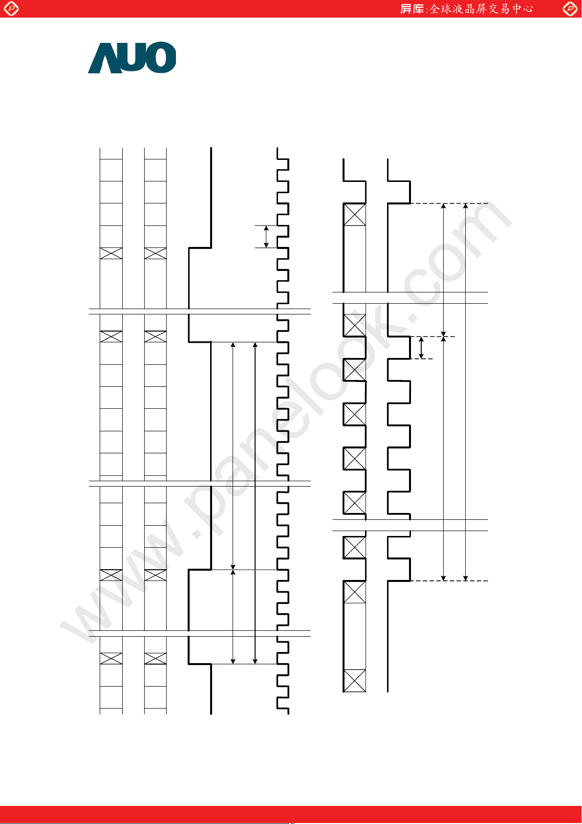
3-3 Signal Timing Specifications
This is the signal timing required at the input of the User connector. All of the interface signal timing should be
satisfied with the following specifications for it’s proper operation.
* Timing Table DE only Mode
Signal
Vertical Section
Horizontal Section
Clock Frequency 1/Tclk 67.2 77.29 80.74
Item Symbol Min Type Max Unit
Period Tv 1090 1130 1392
Active Tdisp (v) 1080
Blanking Tblk (v) 10 50 312
Period Th 550 570 580
Active Tdisp (h) 480
Blanking Tblk (h) 70 90 100
www.panelook.com
Th
Th
Th
Tclk
Tclk
Tclk
MHz
Vertical Frequency Frequency Freq 96 120 122 Hz
Horizontal
Frequency
Notes:
1.) Display position is specific by the rise of DE signal only.
Horizontal display position is specified by the rising edge of 1
the left edge of the screen.
Vertical display position is specified by the rise of DE after a “Low” level period equivalent to eight times of
horizontal period. The 1
top line of screen.
3.) If a period of DEB “High” is less than 1920 DCLK or less than 1080 lines, the rest of the screen displays
black.
4.) The display position does not fit to the screen if a period of DE “High” and the effective data period do not
synchronize with each other.
Frequency Freq 120 135.6 139.2 KHz
st
DCLK after the rise of 1st DE, is displayed on
st
data corresponding to one horizontal line after the rise the of 1st DE is displayed at the
©Copyright AU Optronics, Inc.
April, 2008 All Rights Reserved. T370HW03 V2 17/31
No Reproduction and Redistribution Allowed
One step solution for LCD / PDP / OLED panel application: Datasheet, inventory and accessory!
www.panelook.com
Page 18
Global LCD Panel Exchange Center
www.panelook.com
3-4 Signal Timing Waveforms
RGB Data
(even)
Pixel
M-6
Pixel
M-4
Pixel
M-2
Pixel
M
Invalid Data
Pixel
2
Pixel
4
Pixel
6
(odd)
M-7
M-5
M-3
M-1
1
3
5
RGB Data
DE
Pixel
Pixel
Pixel
Pixel
Invalid Data
Pixel
Pixel
Pixel
CLK
Tclk
Data
Line
Line
Line
N
Invalid Data Invalid Data
1
2
RGB
DE
Th
Tv
Pixel
8
Pixel
10
Pixel
12
Pixel
M-4
Pixel
M-2
Pixel
M
Invalid Data
Pixel
2
Pixel
4
Pixel
7
Pixel
9
Pixel
11
Pixel
M-5
Pixel
M-3
Pixel
M-1
Invalid Data
Pixel
1
Pixel
3
Tdisp(h) Tblk(h)
Th
Line
Line
Line
3
Tdisp(v)Tblk(v)
4
N
©Copyright AU Optronics, Inc.
April, 2008 All Rights Reserved. T370HW03 V2 18/30
No Reproduction and Redistribution Allowed
One step solution for LCD / PDP / OLED panel application: Datasheet, inventory and accessory!
www.panelook.com
Page 19

Global LCD Panel Exchange Center
www.panelook.com
3-5 Color input data assignment
The brightness of each primary color (red, green and blue) is based on the 10 bit gray scale data input for the
color; the higher the binary input, the brighter the color. The table below provides a reference for color versus
data input.
COLOR DATA REFERENCE
Input Color Data
GREEN
MSB LSB
BLUE
MSB LSB
Basic
Color
RED
GREEN
BLUE
Color
R9 R8 R7 R6 R5 R4 R3 R2 R1 R0 G9 G8 G7 G6 G5 G4 G3 G2 G1 G0 B9 B8 B7 B6 B5 B4 B3 B2 B1 B0
Black 0 0 0 0 0 0 0 0 0 0 0 0 0 0 0 0 0 0 0 0 0 0 0 0 0 0 0 0 0 0
Red(1023) 1 1 1 1 1 1 1 1 1 1 0 0 0 0 0 0 0 0 0 0 0 0 0 0 0 0 0 0 0 0
Green(1023) 0 0 0 0 0 0 0 0 0 0 1 1 1 1 1 1 1 1 1 1 0 0 0 0 0 0 0 0 0 0
Blue(1023) 0 0 0 0 0 0 0 0 0 0 0 0 0 0 0 0 0 0 0 0 1 1 1 1 1 1 1 1 1 1
Cyan 0 0 0 0 0 0 0 0 0 0 1 1 1 1 1 1 1 1 1 1 1 1 1 1 1 1 1 1 1 1
Magenta 1 1 1 1 1 1 1 1 1 1 0 0 0 0 0 0 0 0 0 0 1 1 1 1 1 1 1 1 1 1
Yellow 1 1 1 1 1 1 1 1 1 1 1 1 1 1 1 1 1 1 1 1 0 0 0 0 0 0 0 0 0 0
White 1 1 1 1 1 1 1 1 1 1 1 1 1 1 1 1 1 1 1 1 1 1 1 1 1 1 1 1 1 1
RED(0000) 0 0 0 0 0 0 0 0 0 0 0 0 0 0 0 0 0 0 0 0 0 0 0 0 0 0 0 0 0 0
RED(0001) 0 0 0 0 0 0 0 0 0 1 0 0 0 0 0 0 0 0 0 0 0 0 0 0 0 0 0 0 0 0
----
RED(1022) 1 1 1 1 1 1 1 1 1 0 0 0 0 0 0 0 0 0 0 0 0 0 0 0 0 0 0 0 0 0
RED(1023) 1 1 1 1 1 1 1 1 1 1 0 0 0 0 0 0 0 0 0 0 0 0 0 0 0 0 0 0 0 0
GREEN(0000) 0 0 0 0 0 0 0 0 0 0 0 0 0 0 0 0 0 0 0 0 0 0 0 0 0 0 0 0 0 0
GREEN(0001) 0 0 0 0 0 0 0 0 0 0 0 0 0 0 0 0 0 0 0 1 0 0 0 0 0 0 0 0 0 0
----
GREEN(1022) 0 0 0 0 0 0 0 0 0 0 1 1 1 1 1 1 1 1 1 0 0 0 0 0 0 0 0 0 0 0
GREEN(1023) 0 0 0 0 0 0 0 0 0 0 1 1 1 1 1 1 1 1 1 1 0 0 0 0 0 0 0 0 0 0
BLUE(0000) 0 0 0 0 0 0 0 0 0 0 0 0 0 0 0 0 0 0 0 0 0 0 0 0 0 0 0 0 0 0
BLUE(0001) 0 0 0 0 0 0 0 0 0 0 0 0 0 0 0 0 0 0 0 0 0 0 0 0 0 0 0 0 0 1
-------
BLUE(1022) 0 0 0 0 0 0 0 0 0 0 0 0 0 0 0 0 0 0 0 0 1 1 1 1 1 1 1 1 1 0
BLUE(1023) 0 0 0 0 0 0 0 0 0 0 0 0 0 0 0 0 0 0 0 0 1 1 1 1 1 1 1 1 1 1
RED
MSB LSB
©Copyright AU Optronics, Inc.
April, 2008 All Rights Reserved. T370HW03 V2 19/31
No Reproduction and Redistribution Allowed
One step solution for LCD / PDP / OLED panel application: Datasheet, inventory and accessory!
www.panelook.com
Page 20

Global LCD Panel Exchange Center
3-6 Power Sequence of LCD Module
3.6.1 Power Sequence for LCD
www.panelook.com
Power Supply for LCD
Signal
Backlight
90%
10%
t1 t2
Valid Data
t3 t4
Lamp ON
90%
10%
t5 t6 t7
Units
Min.
ms
ms
ms
ms
ms
ms
ms
Min. Typ.
T1
T2
T3
T4
T5
0.4 - 30
0.1 - 50
300 - -
10 - -
0.1 - 50
T6 -
T7
500 - -
Va lu es Parameter
- 300
Note:
The timing controller will not be damaged in case of TV set AC input power suddenly shut down.
Once power reset, it should follow power sequence as spec. definition.
(1) Apply the lamp voltage within the LCD operation range. When the back-light turns on before the LCD
operation or the LCD turns off before the back-light turns off, the display may momentarily become
abnormal screen.
©Copyright AU Optronics, Inc.
April, 2008 All Rights Reserved. T370HW03 V2 20/30
No Reproduction and Redistribution Allowed
One step solution for LCD / PDP / OLED panel application: Datasheet, inventory and accessory!
www.panelook.com
Page 21

Global LCD Panel Exchange Center
4. Optical Specification
Optical characteristics are determined after the unit has been ‘ON’ and stable for approximately 45 minutes in a
dark environment at 25 . The values specified are at an approximate distance 50cm from the LCD surface at a
viewing angle of ĭ and ș equal to 0°.
Testing Condition:
Parameter Symbol Condition
Contrast Ratio
Surface Luminance, white
Gamma 2.1 2.3 2.5
Luminance Variation
Response Time Gray to Gray
Color gamut NTSC 72 %
Color Coordinates
(CIE 1931)
Viewing Angle
©Copyright AU Optronics, Inc.
April, 2008 All Rights Reserved. T370HW03 V2 21/31
No Reproduction and Redistribution Allowed
к
RED
GREEN
BLUE
WHITE
x axis, right
x axis, left
y axis, up
y axis, down
www.panelook.com
FIG.1 Measurement equipment
Val ue
Units Notes
Min. Typ. Max.
CR 4000 5000
LWH
400 500
1
cd/
ф
2
Ӭ
9 pts
WHITE
Tӫ
R
X
R
Y
G
X
G
Y
B
X
B
Y
W
X
W
Y
Ӱ
r
Ӱ
l
Ӱ
u
Ӱ
d
(ӽ=0)
(ӽ=180)
(ӽ=90)
(ӽ=270)
ӽ
=0o, θ=0
Vie wing
Normal angle
CR≥10
o
Typ
-0.03
8
0.64
0.33
0.29
0.6
0.15
0.06
0.280
0.290
89
89
89
89
1.3
3
ms
4
Typ
+0.03
5
Degree
(Ta=25±±±±2oC)
One step solution for LCD / PDP / OLED panel application: Datasheet, inventory and accessory!
www.panelook.com
Page 22

Global LCD Panel Exchange Center
Note:
1. Contrast ratio will be measured in the center of panel (point 5 in Figure 2), Contrast Ratio (CR) is defined
mathematically as:
Contrast Ratio=
2. Surface luminance is luminance value at point 5 across the LCD surface 50cm from the surface with all
pixels displaying white. From more information see FIG 2. When VDDB = 24V, IDDB = 6.04A.
L
=Lo5. Where Lon5 is the luminance with all pixels displaying white at center 5 location.
WH
3. The variation in surface luminance, įWHITE is defined (center of Screen) as:
į
WHITE(9P)
4. Response time TȖ is the average time required for display transition by switching the input signal for five
luminance ratio (0%,25%,50%,75%,100% brightness matrix) and is based on f
= Maximum(L
www.panelook.com
Surface Luminance of
Surface Luminance of
, L
on2
,…,L
on1
L
on5
L
off5
)/ Minimum(L
on9
, L
on1
,…L
on2
=120Hz to optimize.
v
on9
)
5. Viewing angle is the angle at which the contrast ratio is greater than 10. The angles are determined for the
horizontal or x axis and the vertical or y axis with respect to the z axis which is normal to the LCD surface.
For more information see FIG4.
FIG. 2 Luminance measurement positions
The response time is defined as the following figure and shall be measured by switching the input signal for
“any level of gray(bright) “ and “any level of gray(dark)”.
©Copyright AU Optronics, Inc.
April, 2008 All Rights Reserved. T370HW03 V2 22/31
No Reproduction and Redistribution Allowed
One step solution for LCD / PDP / OLED panel application: Datasheet, inventory and accessory!
www.panelook.com
Page 23

Global LCD Panel Exchange Center
www.panelook.com
Any level of gray (Bright)
Any level of gray (Dark)
Any level of gray (Bright)
FIG.3 Measurement of Response Time
FIG.4 Measurement of viewing angle
©Copyright AU Optronics, Inc.
April, 2008 All Rights Reserved. T370HW03 V2 23/31
No Reproduction and Redistribution Allowed
One step solution for LCD / PDP / OLED panel application: Datasheet, inventory and accessory!
www.panelook.com
Page 24

Global LCD Panel Exchange Center
5. Mechanical Characteristics
The contents provide general mechanical characteristics for the model T370HW03 V2. Detailed mechanical
drawings are shown in the following pages.
Outline Dimension
Bezel Opening
Active Display Area
Weight 9,000g (Max.)
www.panelook.com
Horizontal 855.8 mm
Vertical 497.4 mm
Depth 44.9 mm
Horizontal 827.8 mm
Vertical 469.4 mm
Horizontal 819.36 mm
Vertical 460.89 mm
©Copyright AU Optronics, Inc.
April, 2008 All Rights Reserved. T370HW03 V2 24/30
No Reproduction and Redistribution Allowed
One step solution for LCD / PDP / OLED panel application: Datasheet, inventory and accessory!
www.panelook.com
Page 25

Global LCD Panel Exchange Center
Mechanical Figure:
www.panelook.com
©Copyright AU Optronics, Inc.
April, 2008 All Rights Reserved. T370HW03 V2 25/30
No Reproduction and Redistribution Allowed
One step solution for LCD / PDP / OLED panel application: Datasheet, inventory and accessory!
www.panelook.com
Page 26

Global LCD Panel Exchange Center
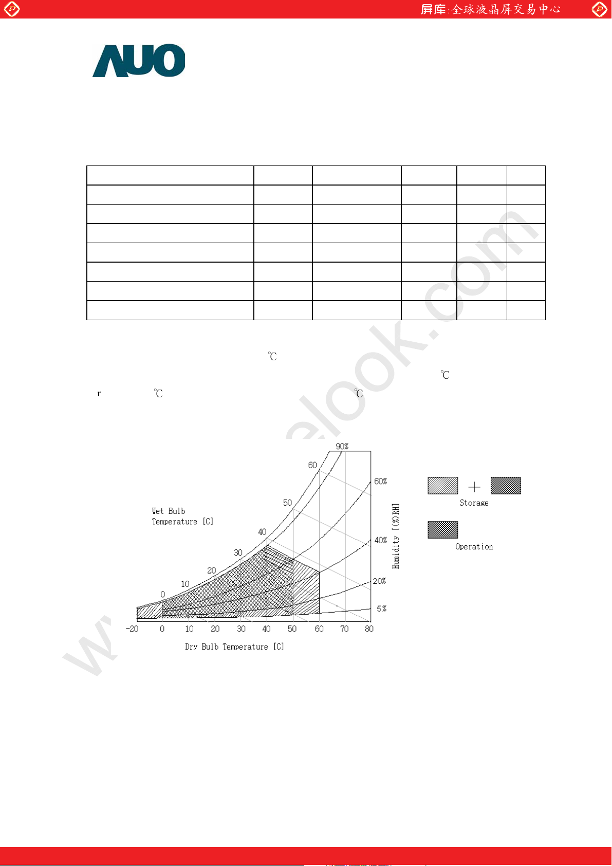
6. Reliability
Environment test condition:
No Test Item Condition
1 High temperature storage test
2 Low temperature storage test
3 Temperature humidity bias test
4 High temperature operation test
5 Low temperature operation test
6
7
8
9
Vibration test
(non-operating)
Shock test
(non-operating)
Vibration test
(with carton)
Drop test
(with carton)
www.panelook.com
к
Ta=6 0
Ta=- 20
Ta=5 0
Ta=5 0
Ta=0
(10 ~ 300Hz/1.5G/11min SR, XYZ 30min/axis)
Vibration level : 1.5G RMS, Bandwidth : 10-300Hz
Duration: X, Y, Z 30min one time each direction
Shock level: 50G
Waveform: half sine wave, 11ms
Direction: ±X, ±Y, ±Z One time each direction
Random wave (1.5Grms 10~200Hz)
30mins / Per each X.Y.Z axes
Height: 30.5 cm
1 corner, 3 edges, 6 surfaces
(ASTMD4169-I)
к
к
к
к
, 300hr
, 300hr
, 300hr
, 80%RH, 300hr
, 300hr
©Copyright AU Optronics, Inc.
April, 2008 All Rights Reserved. T370HW03 V2 26/30
No Reproduction and Redistribution Allowed
One step solution for LCD / PDP / OLED panel application: Datasheet, inventory and accessory!
www.panelook.com
Page 27

Global LCD Panel Exchange Center
7. International Standard
7-1 Safety
(1) UL1950 Third Edition, Underwriters Laboratories, Inc. Jan. 28, 1995
Standard for Safety of Information Technology Equipment Including electrical Business
Equipment.
(2) CAN/CSA C22.2 No. 950-95/60950 Third Edition, Canadian Standards Association,
Standard for Safety of Information Technology Equipment Including Electrical Business
Equipment.
(3) EN60950: 1992+A2: 1993+A2: 1993+C3: 1995+A4: 1997+A11: 1997
IEC 950: 1991+A1: 1992+A2: 1993+C3: 1995+A4:1996
IEC 60065 : vision 7.0
European Committee for Electrotechnical Standardization (CENELEC)
EUROPEAN STANDARD for Safety of Information Technology Equipment Including
Electrical Business Equipment.
7-2 EMC
a) ANSI C63.4 “Methods of Measurement of Radio-Noise Emissions from Low-Voltage
Electrical and Electrical Equipment in the Range of 9kHz to 40GHz. “American National
standards Institute(ANSI), 1992
b) C.I.S.P.R “Limits and Methods of Measurement of Radio Interface Characteristics of
Information Technology Equipment.” International Special committee on Radio
Interference.
c) EN 55022 “Limits and Methods of Measurement of Radio Interface Characteristics of
Information Technology Equipment.” European Committee for Electrotechnical
Standardization. (CENELEC), 1998
www.panelook.com
©Copyright AU Optronics, Inc.
April, 2008 All Rights Reserved. T370HW03 V2 27/30
No Reproduction and Redistribution Allowed
One step solution for LCD / PDP / OLED panel application: Datasheet, inventory and accessory!
www.panelook.com
Page 28

Global LCD Panel Exchange Center
www.panelook.com
8. Packing
A. Panel Label:
TW8601400099-PM0200
TW: T: Taiwan, A/B: China
00099: Panel Serial Number
PM: AUO internal code
B. Carton Label:
T370HW03 V2
©Copyright AU Optronics, Inc.
April, 2008 All Rights Reserved. T370HW03 V2 28/31
No Reproduction and Redistribution Allowed
One step solution for LCD / PDP / OLED panel application: Datasheet, inventory and accessory!
www.panelook.com
Page 29

Global LCD Panel Exchange Center
www.panelook.com
PACKING METHODS:
©Copyright AU Optronics, Inc.
April, 2008 All Rights Reserved. T370HW03 V2 29/31
No Reproduction and Redistribution Allowed
One step solution for LCD / PDP / OLED panel application: Datasheet, inventory and accessory!
www.panelook.com
Page 30
Global LCD Panel Exchange Center
www.panelook.com
Packing Specification:
Item
1 Packing BOX 5 pcs/box 900(L)mm*375(W)mm*610(H)mm 45
2 Pallet 1 1150(L)mm*910(W)mm*140(H)mm 15
3 Boxes per Pallet 6 boxes/Pallet (By Air) ; 9 boxes/Pallet (By Sea)
4 Panels per Pallet 30 pcs/pallet(By Air) ; 45 pcs/Pallet (By Sea)
Pallet after packing 30 (by Air)
Qty. Dimension Weight (kg)
1150(L)mm*910(W)mm*1496(H)mm (by Air)
45 (by Sea)
1150(L)mm*910(W)mm*2244(H)mm (by Sea)
Specification
336 (by Air)
506(by Sea, 40ft
HQ)
Packing
Remark
©Copyright AU Optronics, Inc.
April, 2008 All Rights Reserved. T370HW03 V2 30/31
No Reproduction and Redistribution Allowed
One step solution for LCD / PDP / OLED panel application: Datasheet, inventory and accessory!
www.panelook.com
Page 31

Global LCD Panel Exchange Center
www.panelook.com
9. PRECAUTIONS
Please pay attention to the followings when you use this TFT LCD module.
9-1 MOUNTING PRECAUTIONS
(1) You must mount a module using holes arranged in four corners or four sides.
(2) You should consider the mounting structure so that uneven force (ex. Twisted stress) is not
applied to module. And the case on which a module is mounted should have sufficient strength
so that external force is not transmitted directly to the module.
(3) Please attach the surface transparent protective plate to the surface in order to protect the
polarizer. Transparent protective plate should have sufficient strength in order to the resist
external force.
(4) You should adopt radiation structure to satisfy the temperature specification.
(5) Acetic acid type and chlorine type materials for the cover case are not desirable because the
former generates corrosive gas of attacking the polarizer at high temperature and the latter
causes circuit break by electro-chemical reaction.
(6) Do not touch, push or rub the exposed polarizer with glass, tweezers or anything harder than
HB pencil lead. And please do not rub with dust clothes with chemical treatment. Do not touch
the surface of polarizer for bare hand or greasy cloth. (Some cosmetics are detrimental to the
polarizer.)
(7) When the surface becomes dusty, please wipe gently with absorbent cotton or other soft
materials like chamois soaks with petroleum benzene. Normal-hexane is recommended for
cleaning the adhesives used to attach front/ rear polarizer. Do not use acetone, toluene and
alcohol because they cause chemical damage to the polarizer.
(8) Wipe off saliva or water drops as soon as possible. Their long time contact with polarizer
causes deformations and color fading.
(9) Do not open the case because inside circuits do not have sufficient strength.
9-2 OPERATING PRECAUTIONS
(1) The device listed in the product specification sheets was designed and manufactured for TV
application
(2) The spike noise causes the mis-operation of circuits. It should be lower than following voltage:
V=
200mV(Over and under shoot voltage)
(3) Response time depends on the temperature. (In lower temperature, it becomes longer..)
(4) Brightness of CCFL depends on the temperature. (In lower temperature, it becomes lower.) And
in lower temperature, response time (required time that brightness is stable after turned on)
becomes longer.
(5) Be careful for condensation at sudden temperature change. Condensation makes damage to
polarizer or electrical contacted parts. And after fading condensation, smear or spot will occur.
(6) When fixed patterns are displayed for a long time, remnant image is likely to occur.
(7) Module has high frequency circuits. Sufficient suppression to the electromagnetic interference
shall be done by system manufacturers. Grounding and shielding methods may be important to
minimize the interface.
©Copyright AU Optronics, Inc.
April, 2008 All Rights Reserved. T370HW03 V2 31/31
No Reproduction and Redistribution Allowed
One step solution for LCD / PDP / OLED panel application: Datasheet, inventory and accessory!
www.panelook.com
Page 32

Global LCD Panel Exchange Center
www.panelook.com
9-3 ELECTROSTATIC DISCHARGE CONTROL
Since a module is composed of electronic circuits, it is not strong to electrostatic discharge. Make certain
that treatment persons are connected to ground through wristband etc. And don’t touch interface pin directly.
9-4 PRECAUTIONS FOR STRONG LIGHT EXPOSURE
Strong light exposure causes degradation of polarizer and color filter.
9-5 STORAGE
When storing modules as spares for a long time, the following precautions are necessary.
(1) Store them in a dark place. Do not expose the module to sunlight or fluorescent light. Keep the
к
temperature between 5
(2) The polarizer surface should not come in contact with any other object. It is recommended that they
be stored in the container in which they were shipped.
and 35к at normal humidity.
9-6 HANDLING PRECAUTIONS FOR PROTECTION FILM
(1) The protection film is attached to the bezel with a small masking tape. When the protection film is
peeled off, static electricity is generated between the film and polarizer. This should be peeled off
slowly and carefully by people who are electrically grounded and with well ion-blown equipment or
in such a condition, etc.
(2) When the module with protection film attached is stored for a long time, sometimes there remains a
very small amount of flue still on the Bezel after the protection film is peeled off.
(3) You can remove the glue easily. When the glue remains on the Bezel or its vestige is recognized,
please wipe them off with absorbent cotton waste or other soft material like chamois soaked with
normal-hexane.
©Copyright AU Optronics, Inc.
April, 2008 All Rights Reserved. T370HW03 V2 32/31
No Reproduction and Redistribution Allowed
One step solution for LCD / PDP / OLED panel application: Datasheet, inventory and accessory!
www.panelook.com
Page 33

Global LCD Panel Exchange Center
www.panelook.com
Appendix :
1. Deep (10%) dimming life time
©Copyright AU Optronics, Inc.
April, 2008 All Rights Reserved. T370HW03 V2 33/31
No Reproduction and Redistribution Allowed
One step solution for LCD / PDP / OLED panel application: Datasheet, inventory and accessory!
www.panelook.com
 Loading...