

Page 1

Global LCD Panel Exchange Center
www.panelook.com
Product Specifications
37.0” HDTV Color TFT-LCD Module
Model Name: T370HW01
V.0
(*) Preliminary Specifications
( ) Final Specifications
Note: This Specification is subject to change without notice.
©Copyright AU Optronics, Inc.
March, 2004 All Rights Reserved. T370HW01 V.0 Ver0 0/25
No Reproduction and Redistribution Allowed
One step solution for LCD / PDP / OLED panel application: Datasheet, inventory and accessory!
www.panelook.com
Page 2
Global LCD Panel Exchange Center
www.panelook.com
Contents
ITEM No
COVER
CONTENTS
RECORD OF REVISIONS
GENERAL DESCRIPTION 1
ABSOLUTE MAXIMUM RATINGS 2
ELECTRICAL SPECIFICATIONS 3
ELECTRICAL CHARACTREISTICS 3-1
INTERFACE CONNECTIONS 3-2
INPUT TIMING SPECIFICATIONS 3-3
COLOR INPUT DATA REFERNECE 3-5
SIGNAL TIMING WAVEFORMS 3-4
POWER SEQUENCE 3-6
OPTICAL SFECIFICATIONS 4
©Copyright AU Optronics, Inc.
March, 2004 All Rights Reserved. T370HW01 V.0 Ver0 1/25
No Reproduction and Redistribution Allowed
MECHANICAL CHARACTERISTICS 5
RELIABLITY 6
INTERNATIONAL STANDARDS 7
SAFETY 7-1
EMC 7-2
Packing 8
PRECAUTIONS 9
One step solution for LCD / PDP / OLED panel application: Datasheet, inventory and accessory!
www.panelook.com
Page 3
Global LCD Panel Exchange Center
Version Date No Description Remark
0.1 Sep. 26,’03 First Draft (Preliminary)
www.panelook.com
Record of Revision
©Copyright AU Optronics, Inc.
March, 2004 All Rights Reserved. T370HW01 V.0 Ver0 2/25
No Reproduction and Redistribution Allowed
One step solution for LCD / PDP / OLED panel application: Datasheet, inventory and accessory!
www.panelook.com
Page 4
Global LCD Panel Exchange Center
1. General Description
This specification applies to the 37.0 inch Color TFT-LCD Module T370HW01. This LCD
module has a TFT active matrix type liquid crystal panel 1920x1080 pixels, and diagonal size
of 37.0 inch. This module supports 1920x1080 HDTV mode (Non-interlace).
Each pixel is divided into Red, Green and Blue sub-pixels or dots which are arranged in
vertical stripes. Gray scale or the brightness of the sub-pixel color is determined with a 8-bit
gray scale signal for each dot.
The T370HW01 has been designed to apply the 8-bit 2 channel LVDS interface method. It is
intended to support displays where high brightness, wide viewing angle, high color saturation,
and high color depth are very important.
www.panelook.com
*
General Information
Items Specification Unit Note
Active Screen Size 37.01 Inches
Display Area 894.8 (H) x 460.89(V) mm
Outline Dimension 894.8(H) x 527.4(V) x 50.5(D) mm With inverter
Driver Element a-Si TFT active matrix
Display Colors 16.7M Colors
Number of Pixels 1920 x 1080 Pixel
Pixel Arrangement RGB vertical stripe
Pixel pitch 0.42675(H) x 0.42675(W)
Surface Treatment Hard-Coating (3H), Anti-Glare,
Reflectance < 2%
©Copyright AU Optronics, Inc.
March, 2004 All Rights Reserved. T370HW01 V.0 Ver0 3/25
No Reproduction and Redistribution Allowed
One step solution for LCD / PDP / OLED panel application: Datasheet, inventory and accessory!
www.panelook.com
Page 5
Global LCD Panel Exchange Center
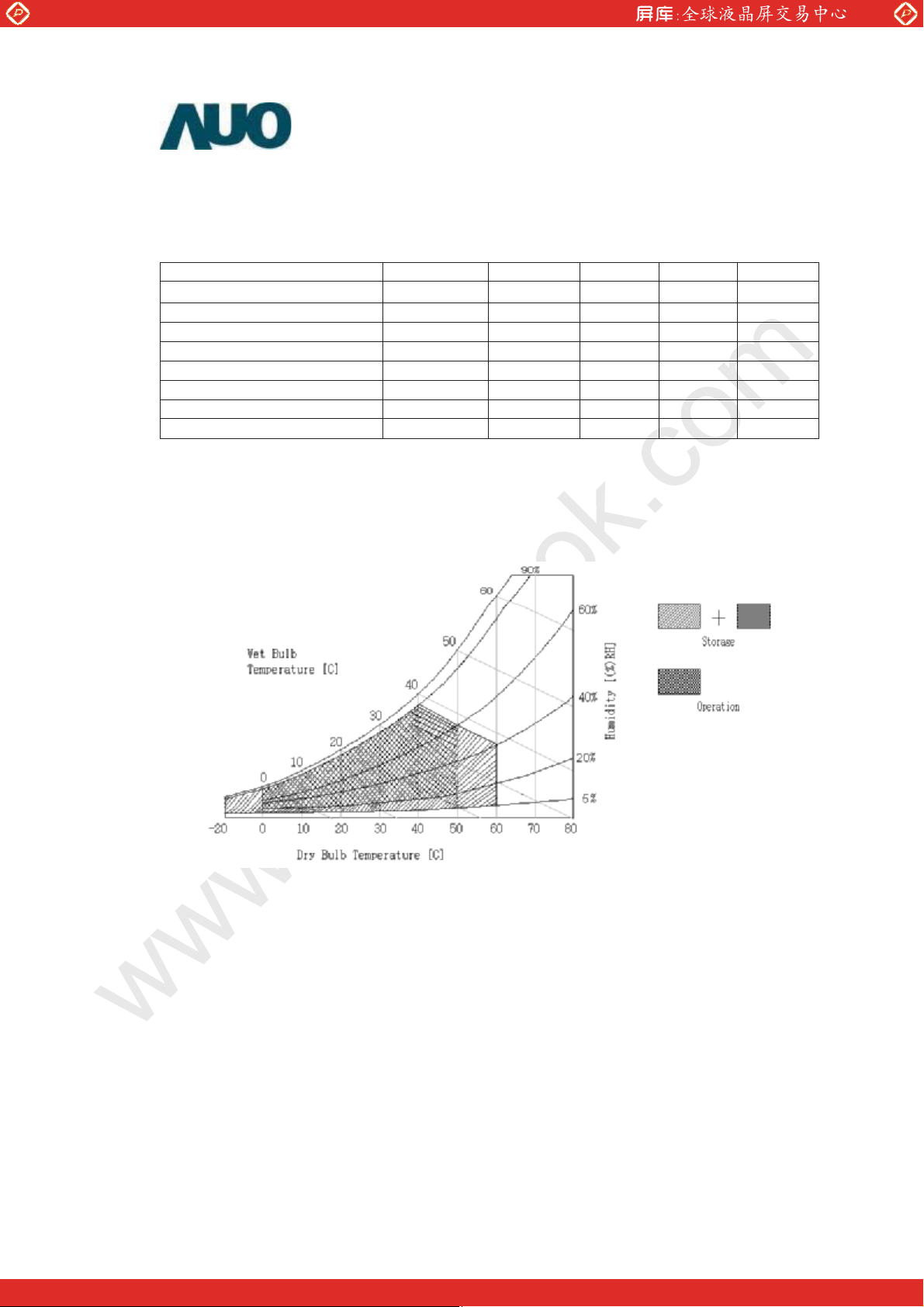
2. Absolute Maximum Ratings
The following are maximum values which, if exceeded, may cause faulty operation or
damage to the unit.
Parameter Symbol Min. Max. Unit Note
Logic/LCD Driving Voltage VDD 10.8 13.2
Signal Input Voltage Vin
BLU Input Voltage V
BLU Control Voltage BL
Operating Temperature TOP 00 50
Storage Temperature HST -20 60
Operating Ambient Humidity HOP 10 90
Storage Humidity HST 10 90
Note: 1. Temperature and relative humidity range are shown in the figure below. Wet bulb
temperature should be 39
www.panelook.com
DDB
ON
V
V
V
V
1
1
%RH 1
%RH 1
dc
At 255
©Copyright AU Optronics, Inc.
March, 2004 All Rights Reserved. T370HW01 V.0 Ver0 4/25
No Reproduction and Redistribution Allowed
One step solution for LCD / PDP / OLED panel application: Datasheet, inventory and accessory!
www.panelook.com
Page 6
Global LCD Panel Exchange Center
3. Electrical Specification
3-1 Electrical Characteristics
The T460HW01 requires two power inputs. One is employed to power the LCD electronics and to drive
the TFT array and liquid crystal. The second input which powers the CCFL, is typically generated by an
inverter.
www.panelook.com
Parameter Symbol
Min Typ Max
LCD:
Power Supply Input Voltage Vcc 10.80 12.0 13.20 Vdc
Power Supply Input Current Icc - 1.0 A 1
Power Consumption Pc - 12.0 Watt 1
Inrush Current I
Backlight Power Consumption 140 2
Life Time 60,000 3
Note:
1. The specified current and power consumption are under the Vcc=12.0V, 25, fv= 60Hz,
fCLK=65Mhz condition whereas mosaic pattern (8x6) is displayed and fv is the frame frequency.
- - TBD MA peak
RUSH
Values
Unit Notes
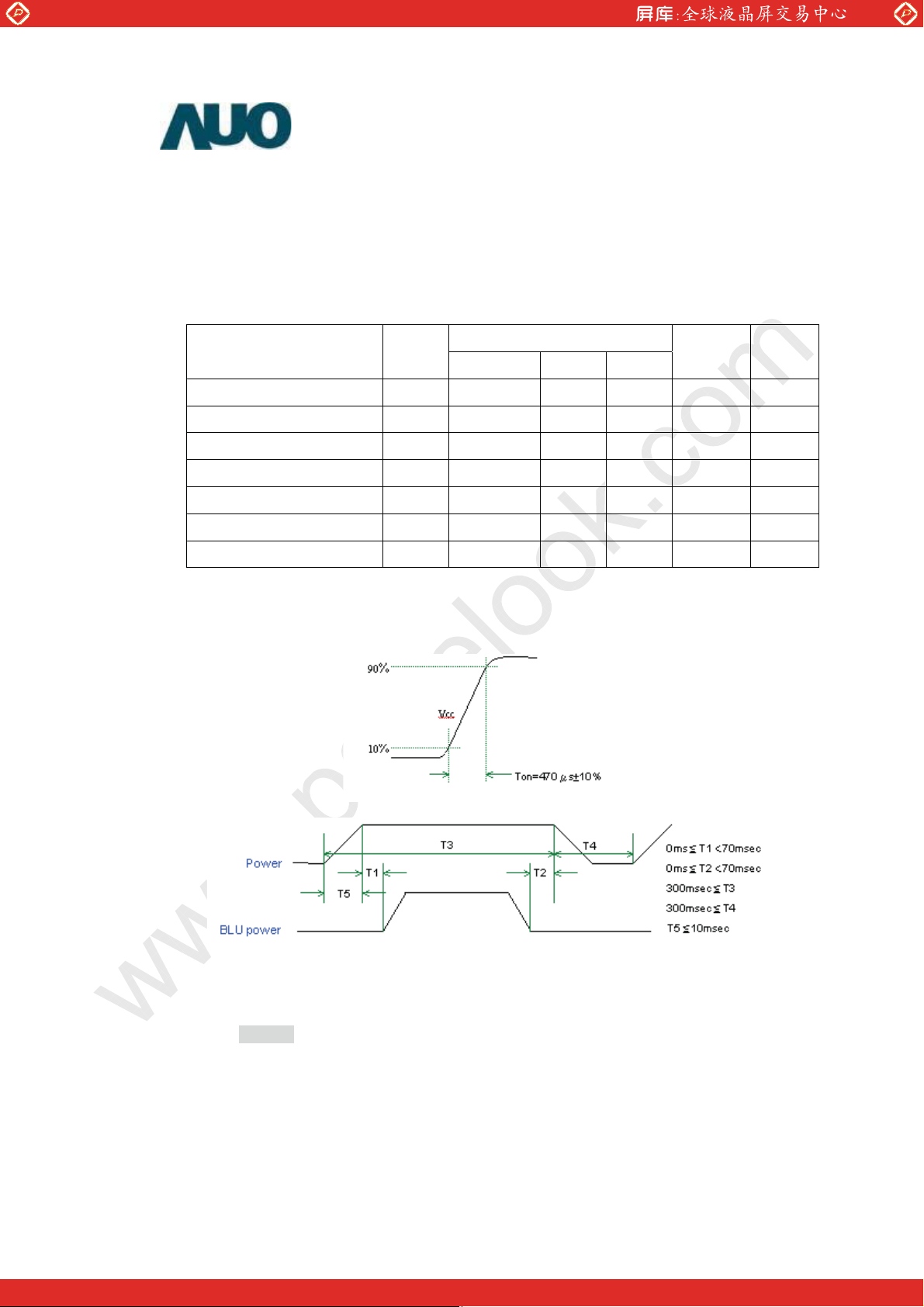
Sequence of Power-on/off and signal-on/off
Apply the lamp voltage within the LCD operating range. When the backlight turns on before the
LCD operation or the LCD turns off before the backlight turns off, the display may momentarily
become abnormal.
Caution:
In case of handling, make sure to turn off the power when you plug the cable into the input
connector or pull the cable out of the connector.
2. The lamp power consumption shown above does include loss of external inverter at 25.
©Copyright AU Optronics, Inc.
March, 2004 All Rights Reserved. T370HW01 V.0 Ver0 5/25
No Reproduction and Redistribution Allowed
The above on/off sequence should be applied to avoid abnormal function in the display.
The used lamp current is the lamp typical current
One step solution for LCD / PDP / OLED panel application: Datasheet, inventory and accessory!
www.panelook.com
Page 7

Global LCD Panel Exchange Center
www.panelook.com
3. The life is determined as the time at which luminance of the lamp is 50% compared to that of
Note:
The design of the inverter must have specifications for the lamp in LCD Assembly. The performance of the
Lamp in LCM, for example lifetime or brightness, is extremely influenced by the characteristics of the
DC-AC Inverter. So all the parameters of an inverter should be carefully designed so as not to produce too
much leakage current from high-voltage output of the inverter. When you design or order the inverter,
please make sure unwanted lighting caused by the mismatch of the lamp and the inverter (no lighting,
flicker, etc) never occurs. When you confirm it, the LCD Assembly should be operated in the same
condition as installed in your instrument.
Do not attach a conducting tape to lamp connecting wire. If the lamp wire attach to conducting tape,
TFT-LCD Module have a low luminance and the inverter has abnormal action because leakage current
occurs between lamp wire and conducting tape.
The relative humidity must not exceed 80% non-condensing at temperatures of 40 or less. At
temperatures greater than 40, the wet bulb temperature must not exceed 39. When operate at low
temperatures, the brightness of CCFL will drop and the lifetime of CCFL will be reduced.
The output of the inverter must have symmetrical (negative and positive) voltage waveform and
symmetrical current waveform (Asymmetry ratio is less than 10%). Please do not use the inverter that has
asymmetrical voltage and asymmetrical current and spike wave. Requirements for a system inverter design
which is intended to have a better display performance, a better power efficiency and a more reliable lamp.
It shall help increase the lamp lifetime and reduce its leakage current.
a. The asymmetry rate of the inverter current and voltage waveform should be 10% below;
b. The distortion rate of the current and voltage waveform should be within 210%;
c. The ideal sine current and voltage waveform shall be symmetric in positive and negative
initial value at the typical lamp current on condition of continuous operating at 252
polarities.
©Copyright AU Optronics, Inc.
March, 2004 All Rights Reserved. T370HW01 V.0 Ver0 6/25
No Reproduction and Redistribution Allowed
One step solution for LCD / PDP / OLED panel application: Datasheet, inventory and accessory!
www.panelook.com
Page 8
Global LCD Panel Exchange Center
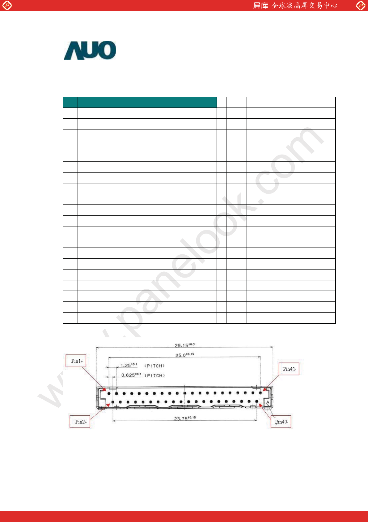
3-2 Interface Connections
LCD Connector (CN1): FI-WE41P-HF(JAE) or equivalent
LVDS Transmitter:
PIN # Spec NAME DESCRIPTION / Reserve function 21 RxE1- Negative LVDS data input (Even data)
1 NC No Connecting Pin* 22 RxE1+ Positive LVDS data input (Even data)
2 NC No Connecting Pin* 23 RxE2- Negative LVDS data input (Even data)
3 NC No Connecting Pin* 24 RxE2+ Positive LVDS data input (Even data)
4 GND Power Ground 25 GND Power Ground
5 RxO0- Negative LVDS data input (Odd data) 26 RxEC- Negative LVDS clock input (Even clock)
6 RxO0+ Positive LVDS data input (Odd data) 27 RxEC+ Positive LVDS clock input (Even clock)
7 RxO1- Negative LVDS data input (Odd data) 28 RxE3- Negative LVDS data input (Even data)
www.panelook.com
8 RxO1+ Positive LVDS data input (Odd data) 29 RxE3+ Positive LVDS data input (Even data)
9 RxO2- Negative LVDS data input (Odd data, HS, VS, DE) 30 NC No Connecting Pin*
10 RxO2+ Positive LVDS data input (Odd data, HS, VS, DE) 31 NC No Connecting Pin*
11 GND Power Ground 32 GND Power Ground
12 RxOC- Negative LVDS clock input (Odd clock) 33 NC No Connecting Pin*
13 RxOC+ Positive LVDS clock input (Odd clock) 34 NC No Connecting Pin*
14 RxO3- Negative LVDS data input (Odd data) 35 GND Power Ground
15 RxO3+ Positive LVDS data input (Odd data) 36 GND Power Ground
16 NC No Connecting Pin* 37 GND Power Ground
17 NC No Connecting Pin* 38 POWER 12V Power Input
18 GND Power Ground 39 POWER 12V Power Input
19 RxE0- Negative LVDS data input (Even data) 40 POWER 12V Power Input
20 RxE0+ Positive LVDS data input (Even data) 41 POWER 12V Power Input
*NC Only – Pull High or Low is not allowed
Note: All GND (ground) pins should be connected together and also be connected to the LCD’s metal
frame.
All Vcc (power input) pins should be connected together.
©Copyright AU Optronics, Inc.
March, 2004 All Rights Reserved. T370HW01 V.0 Ver0 7/25
No Reproduction and Redistribution Allowed
One step solution for LCD / PDP / OLED panel application: Datasheet, inventory and accessory!
www.panelook.com
Page 9

Global LCD Panel Exchange Center
www.panelook.com
LVDS Order
RCLKP1
RAP1
RBP1
RCP1
RDP1
RCLKP2
RAP2
RBP2
RCP2
RDP2
G0 R5 R4 R3 R2 R1 R0
B1 B0 G5 G4 G3 G2 G1
DE VS HS B5 B4 B3 B2
RSV B7 B6 G7 G6 R7 R6
G0 R5 R4 R3 R2 R1 R0
B1 B0 G5 G4 G3 G2 G1
B5 B4 B3 B2
RSV B7 B6 G7 G6 R7 R6
©Copyright AU Optronics, Inc.
March, 2004 All Rights Reserved. T370HW01 V.0 Ver0 8/25
No Reproduction and Redistribution Allowed
One step solution for LCD / PDP / OLED panel application: Datasheet, inventory and accessory!
www.panelook.com
Page 10

Global LCD Panel Exchange Center
BACKLIGHT CONNECTOR PIN CONFIGURATION
1. Electrical specification
No Item Symbol Test Condition Min Typ Max Unit Note
1 Input Voltage Vin 21.6 24 26.4 V
2 Input Current Iin VDD=24V,DimMax - - tbd mA
3 Input Power Pin VDD=24V,DimMax - - tbd W
4 Input Protection Voltage Vin *1 - 17 - 27 V
5 Output Working Voltage VL *2 VDD=24V,DimMax - 1400 - Vrms
www.panelook.com
-
Ta=255
6 Output Current *3
7 Strike Voltage VS *2 VDD=24V,DimMax 1600 - - Vrms
8 Open Lamp Voltage Vopen
9 Oscillating Frequency FO VDD=24V,DimMax 64 67 70 kHz
10 Dimming Frequency FB VDD=24V 150 - 300 Hz
11 Inverter Sync Frequency InvSync*5 VDD=24V 128 134 140 kHz
12 Striking Time Ts *2 VDD=24V,DimMax - 1.5 - sec
13 On/Off Control Voltage
14 Analog Dimming Control *6
15 PWM Dimming Control *6
16 TTL Test Loading Rload VDD=24V >10 kohm
1: Connection of brightness control terminal
Bright control by the voltage
5.0V : Min. brightness
0V : Max. brightness
OPEN : Max. brightness
2: BLON Logic
H(5V) : Back Light ON
L (0V) : Back Light OFF
OPEN : Back Light OFF
IL(Max) VDD=24V,DimMax - 6.0 -
IL(Min) VDD=24V,DimMin - 2.5 -
VDD=24V, 0
On BLON VDD=24V 2 - 5 V
Off BLON VDD=24V 0 - 0.8 V
Max Vdim VDD=24V - 0 - V or Open
Min Vdim VDD=24V 4.75 5 5.25 V
Max Vdim VDD=24V - 100 - %
Min Vdim VDD=24V - 30 - % Duty Ratio
- 2400 - Vrms
mArms
©Copyright AU Optronics, Inc.
March, 2004 All Rights Reserved. T370HW01 V.0 Ver0 9/25
No Reproduction and Redistribution Allowed
One step solution for LCD / PDP / OLED panel application: Datasheet, inventory and accessory!
www.panelook.com
Page 11

Global LCD Panel Exchange Center
3. Input specification
www.panelook.com
3-3 Input Timing Specifications
This is the signal timing required at the input of the User connector. All of the interface signal timing should be
satisfied with the following specifications for it’s proper operation.
Timing Table
(1) DE mode
Frame Rate = 60 Hz
Signal Item Symbol Min. Typ. Max. Unit
Vertical Period TV
Section Active Tdisp(V)
Blanking Tblk(V)
Horizontal Period Th
Section Active Tdisp(h)
1088 1130 1200
1080 1080 1080
8 50 120
1000 1100 1180
960 960 960
Th
Th
Th
Tclk
Tclk
Blanking Tblk(h)
Period Tclk
Clock Freqency Freq
©Copyright AU Optronics, Inc.
March, 2004 All Rights Reserved. T370HW01 V.0 Ver0 10/25
No Reproduction and Redistribution Allowed
40 140 220
15.32 11.76
65.28 85
Tclk
MHz
ns
One step solution for LCD / PDP / OLED panel application: Datasheet, inventory and accessory!
www.panelook.com
Page 12

Global LCD Panel Exchange Center
(
)
www.panelook.com
3-4 Signal Timing Waveforms
CLKP-CLKN
RSDS
tSETUP2
tHOLD2
DIO1;SHL=H
DIO2;SHL=L
D00P-
D00N
D01PD01N
D02P-
D02N
D03P-
D03N
D10P-
D10N
D11P-
D11N
50%
50%
tSETUP1
tSETUP1
tHOLD1
R(0) R(1)
R(2) R(3)
R(4) R(5)
R(6) R(7) R(6) R(7) R(6) R(7) R(6)
G(0) G(1)
G(2) G(3)
tHOLD1
R(0) R(1)
R(2) R(3)
R(4) R(5)
G(0) G(1)
G(2) G(3)
PWCLK(L) PWCLK(H)
PWCLK
R(0) R(1)
R(2) R(3)
R(4) R(5)
G(0) G(1)
G(2) G(3)
VIH
VCM
VIL
VIH
VCM
VIL
R(2)
R(4)
G(0)
G(2)
D12P-
D12N
D13P-
D13N
D20P-
D20N
D21P-
D21N
D22P-
D22N
D23P-
D23N
G(4) G(5)
G(4) G(5)
G(4) G(5)
G(4)
G(6) G(7) G(6) G(7) G(6) G(7) G(6)
B(0) B(1)
B(2) B(3)
B(4) B(5)
B(0) B(1)
B(2) B(3)
B(4) B(5)
B(0) B(1)
B(2) B(3)
B(4) B(5)
B(0)
B(2)
B(4)
B(6) B(7) B(6) B(7) B(6) B(7) B(6)
1st
Data
2nd
Data
3rd
Data
©Copyright AU Optronics, Inc.
March, 2004 All Rights Reserved. T370HW01 V.0 Ver0 11/25
No Reproduction and Redistribution Allowed
One step solution for LCD / PDP / OLED panel application: Datasheet, inventory and accessory!
www.panelook.com
Page 13

Global LCD Panel Exchange Center
3-5 Color Input Data Reference
The brightness of each primary color (red, green and blue) is based on the 8 bit gray scale data input for the
color; the higher the binary input, the brighter the color. The table below provides a reference for color versus
data input.
www.panelook.com
COLOR DATA REFERENCE
Color
Basic
Color
RED
Input Color Data
RED
MSB LSB
R7 R6 R5 R4 R3 R2 R1 R0 G7 G6 G5 G4 G3 G2 G1 G0 B7 B6 B5 B4 B3 B2 B1 B0
Black 0 0 0 0 0 0 0 0 0 0 0 0 0 0 0 0 0 0 0 0 0 0 0 0
Red(255) 1 1 1 1 1 1 1 1 0 0 0 0 0 0 0 0 0 0 0 0 0 0 0 0
Green(255) 0 0 0 0 0 0 0 0 1 1 1 1 1 1 1 1 0 0 0 0 0 0 0 0
Blue(255) 0 0 0 0 0 0 0 0 0 0 0 0 0 0 0 0 1 1 1 1 1 1 1 1
Cyan 0 0 0 0 0 0 0 0 1 1 1 1 1 1 1 1 1 1 1 1 1 1 1 1
Magenta 1 1 1 1 1 1 1 1 0 0 0 0 0 0 0 0 1 1 1 1 1 1 1 1
Yellow 1 1 1 1 1 1 1 1 1 1 1 1 1 1 1 1 0 0 0 0 0 0 0 0
White 1 1 1 1 1 1 1 1 1 1 1 1 1 1 1 1 1 1 1 1 1 1 1 1
RED(000) 0 0 0 0 0 0 0 0 0 0 0 0 0 0 0 0 0 0 0 0 0 0 0 0
RED(001) 0 0 0 0 0 0 0 0 0 0 0 0 0 0 0 0 0 0 0 0 0 0 0 0
----
RED(254) 1 1 1 1 1 1 1 0 0 0 0 0 0 0 0 0 0 0 0 0 0 0 0 0
RED(255) 1 1 1 1 1 1 1 1 0 0 0 0 0 0 0 0 0 0 0 0 0 0 0 0
MSB LSB
GREEN
BLUE
MSB LSB
GREEN
BLUE
©Copyright AU Optronics, Inc.
March, 2004 All Rights Reserved. T370HW01 V.0 Ver0 12/25
No Reproduction and Redistribution Allowed
GREEN(000) 0 0 0 0 0 0 0 0 0 0 0 0 0 0 0 0 0 0 0 0 0 0 0 0
GREEN(001) 0 0 0 0 0 0 0 0 0 0 0 0 0 0 0 1 0 0 0 0 0 0 0 0
----
GREEN(254) 0 0 0 0 0 0 0 0 1 1 1 1 1 1 1 0 0 0 0 0 0 0 0 0
GREEN(255) 0 0 0 0 0 0 0 0 1 1 1 1 1 1 1 1 0 0 0 0 0 0 0 0
BLUE(000) 0 0 0 0 0 0 0 0 0 0 0 0 0 0 0 0 0 0 0 0 0 0 0 0
BLUE(001) 0 0 0 0 0 0 0 0 0 0 0 0 0 0 0 0 0 0 0 0 0 0 0 1
-------
BLUE(254) 0 0 0 0 0 0 0 0 0 0 0 0 0 0 0 0 1 1 1 1 1 1 1 0
BLUE(255) 0 0 0 0 0 0 0 0 0 0 0 0 0 0 0 0 1 1 1 1 1 1 1 1
One step solution for LCD / PDP / OLED panel application: Datasheet, inventory and accessory!
www.panelook.com
Page 14

Global LCD Panel Exchange Center
3-6 Power Sequence
LCD Vcc
10%
www.panelook.com
10ms
min.
90% 90%
10%
10%
30 max, 1ms min.
Signal
Lamp On
0 min.
170ms min.
0 min.
10% 10%
0 min.
10% 10%
©Copyright AU Optronics, Inc.
March, 2004 All Rights Reserved. T370HW01 V.0 Ver0 13/25
No Reproduction and Redistribution Allowed
One step solution for LCD / PDP / OLED panel application: Datasheet, inventory and accessory!
www.panelook.com
Page 15

Global LCD Panel Exchange Center
4. Optical Specification
Optical characteristics are determined after the unit has been ‘ON’ and stable for approximately 30 minutes in a
dark environment at 25. The values specified are at an approximate distance 50cm from the LCD surface at a
viewing angle of and equal to 0.
Fig.1 1 presents additional information concerning the measurement equipment and method.
www.panelook.com
Parameter
Symbol
Values
Min. Typ. Max.
Units Notes
Contrast Ratio CR 800 1
Surface Luminance, white LWH 550
Luminance Variation
Response Time
WHITE
5 p 1.3 3
Gray to Gray 12
Tr 15
Tf 10
Color
Chromaticity
RED RX 0.640
R
0.330
Y
GREEN GX 0.290
G
0.600
Y
Typ –0.03
Typ +0.03
cd/
ms
2
BLUE BX 0.150
B
0.060
Y
WHITE WX 0.280
W
Y
0.290
Viewing Angle
x axis, right(=0) r
x axis, left(=180) l
y axis, up(=90)
y axis, down (=0)
u
d
85 Degree 5
85
85
85
©Copyright AU Optronics, Inc.
March, 2004 All Rights Reserved. T370HW01 V.0 Ver0 14/25
No Reproduction and Redistribution Allowed
One step solution for LCD / PDP / OLED panel application: Datasheet, inventory and accessory!
www.panelook.com
Page 16

Global LCD Panel Exchange Center
Note: 1. Contrast Ratio (CR) is defined mathematically as:
Contrast Ratio=
1. Surface luminance is luminance value at point 1 across the LCD surface 50cm from the surface with
all pixels displaying white. From more information see FIG 2.
2. The variation in surface luminance, WHITE is defined (center of Screen) as:
www.panelook.com
Surface Luminance with all white pixels
Surface Luminance with all black pixels
WHITE(5P)
3. Response time is the time required for the display to transition from white to black (Rise Time, Tr
and from black to white (Decay Time, Tr
4. Viewing angle is the angle at which the contrast ratio is greater than 5. The angles are determined for
the horizontal or x axis and the vertical or y axis with respect to the z axis which is normal to the LCD
surface. For more information see FIG4.
=Maximum(L
, L
on1
,…,L
on2
). For additional information see FIG3.
D
)/Minimum(L
on5
on1
, L
on2
,…L
on5
)
)
R
©Copyright AU Optronics, Inc.
March, 2004 All Rights Reserved. T370HW01 V.0 Ver0 15/25
No Reproduction and Redistribution Allowed
One step solution for LCD / PDP / OLED panel application: Datasheet, inventory and accessory!
www.panelook.com
Page 17

Global LCD Panel Exchange Center
FIG. 2 Luminance
www.panelook.com
FIG.3 Response Time
The response time is defined as the following figure and shall be measured by switching the input signal for
“black” and “white”.
©Copyright AU Optronics, Inc.
March, 2004 All Rights Reserved. T370HW01 V.0 Ver0 16/25
No Reproduction and Redistribution Allowed
One step solution for LCD / PDP / OLED panel application: Datasheet, inventory and accessory!
www.panelook.com
Page 18

Global LCD Panel Exchange Center
FIG.4 Viewing angle
www.panelook.com
©Copyright AU Optronics, Inc.
March, 2004 All Rights Reserved. T370HW01 V.0 Ver0 17/25
No Reproduction and Redistribution Allowed
One step solution for LCD / PDP / OLED panel application: Datasheet, inventory and accessory!
www.panelook.com
Page 19

Global LCD Panel Exchange Center
5. Mechanical Characteristics
The contents provide general mechanical characteristics for the model T460HW01. In addition the figures in the
next page are detailed mechanical drawing of the LCD.
www.panelook.com
Outline Dimension
Wei gh t 12000g (Typ.)
Surface Treatment Hard-Coating (3H), Anti-Glare, Reflectance < 2%
Horizontal 894.8 mm
Vertical 527.4 mm
Depth 50.5 mm(with inverter)
Horizontal 827.8 mm Bezel Area
Vertical 527.4 mm
Horizontal 819.36 mm Active Display Area
Vertical 460.89 mm
©Copyright AU Optronics, Inc.
March, 2004 All Rights Reserved. T370HW01 V.0 Ver0 18/25
No Reproduction and Redistribution Allowed
One step solution for LCD / PDP / OLED panel application: Datasheet, inventory and accessory!
www.panelook.com
Page 20

Global LCD Panel Exchange Center
2-D Drawing
www.panelook.com
©Copyright AU Optronics, Inc.
March, 2004 All Rights Reserved. T370HW01 V.0 Ver0 19/25
No Reproduction and Redistribution Allowed
One step solution for LCD / PDP / OLED panel application: Datasheet, inventory and accessory!
www.panelook.com
Page 21

Global LCD Panel Exchange Center
6. Reliability
Environment test condition
No Test Item Condition
1 High temperature storage test
2 Low temperature storage test
www.panelook.com
Ta=60 240h
Ta= -20 240h
3 High temperature operation test
4 Low temperature operation test
5 Vibration test
(non-operating)
6 Shock test
(non-operating)
7 Vibration test
(with carton)
8 Altitude
Storage/shipment
Result Evaluation Criteria
There should be no change which might affect the practical display function when the display quality test is
conducted under normal operating condition.
Ta=50 50%RH 240h
Ta=0 240h
Wave form: random
Vibration level: 1.5G RMS
Bandwidth: 10-300Hz,
Sweep time: 10min
Duration: X, Y, Z 30min
One time each direction
Shock level: 50G
Waveform: half since wave, 11ms
Direction: X, Y, Z
One time each direction
TBD
TBD
©Copyright AU Optronics, Inc.
March, 2004 All Rights Reserved. T370HW01 V.0 Ver0 20/25
No Reproduction and Redistribution Allowed
One step solution for LCD / PDP / OLED panel application: Datasheet, inventory and accessory!
www.panelook.com
Page 22

Global LCD Panel Exchange Center
7. International Standard
7-1. Safety
1. UL 60950, Third Edition, Underwriters Laboratories, Inc. Dec. 11, 2000.
Standard for Safety of Information Technology Equipment, including Electrical Business Equipment.
2. CAN/CSA C22.2 No. 60950, Third Edition, Canadian Standards Association, Dec. 1, 2000
Standard for Safety of Information Technology Equipment Including Electrical Business Equipment.
3. EN60950: 2000, Third Edition
IEC 60950:1999, Third Edition
European Committee for Electrotechnical Standardization (CENELEC)
EUROPEAN STANDARD for Safety of Information Technology Equipment Including Electrical
Business Equipment.
www.panelook.com
7-2. EMC
a) ANSI C63.4 “Methods of Measurement of Radio-Noise Emissions from Low-Voltage Electrical and
Electrical Equipment in the Range of 9kHz to 40GHz. “American National standards Institute
(ANSI), 1992
b) C.I.S.P.R “Limits and Methods of Measurement of Radio Interface Characteristics of Information
Technology Equipment.” International Special committee on Radio Interference.
c) EN 55022 “Limits and Methods of Measurement of Radio Interface Characteristics of Information
Technology Equipment.” European Committee for Electrotechnical Standardization. (CENELEC),
1998
©Copyright AU Optronics, Inc.
March, 2004 All Rights Reserved. T370HW01 V.0 Ver0 21/25
No Reproduction and Redistribution Allowed
One step solution for LCD / PDP / OLED panel application: Datasheet, inventory and accessory!
www.panelook.com
Page 23

Global LCD Panel Exchange Center
6. Packing
(1) Label Sample
TBD
(2) Carton Label
TBD
(3) Carton Size
TBD
www.panelook.com
©Copyright AU Optronics, Inc.
March, 2004 All Rights Reserved. T370HW01 V.0 Ver0 22/25
No Reproduction and Redistribution Allowed
One step solution for LCD / PDP / OLED panel application: Datasheet, inventory and accessory!
www.panelook.com
Page 24

Global LCD Panel Exchange Center
7. PRECAUTIONS
Please pay attention to the followings when you use this TFT LCD module.
9-1 MOUNTING PRECAUTIONS
(1) You must mount a module using holes arranged in four corners or four sides.
(2) You should consider the mounting structure so that uneven force (ex. Twisted stress) is not
applied to module. And the case on which a module is mounted should have sufficient strength so
that external force is not transmitted directly to the module.
(3) Please attach the surface transparent protective plate to the surface in order to protect the
polarizer. Transparent protective plate should have sufficient strength in order to the resist external
force.
(4) You should adopt radiation structure to satisfy the temperature specification.
(5) Acetic acid type and chlorine type materials for the cover case are not desirable because the
former generates corrosive gas of attacking the polarizer at high temperature and the latter
causes circuit break by electro-chemical reaction.
(6) Do not touch, push or rub the exposed polarizers with glass, tweezers or anything harder than
HB pencil lead. And please do not rub with dust clothes with chemical treatment. Do not touch
the surface of polarizer for bare hand or greasy cloth. (Some cosmetics are detrimental to the
polarizer.)
(7) When the surface becomes dusty, please wipe gently with absorbent cotton or other soft
materials like chamois soaks with petroleum benzene. Normal-hexane is recommended for
cleaning the adhesives used to attach front/ rear polarizers. Do not use acetone, toluene and
alcohol because they cause chemical damage to the polarizer.
(8) Wipe off saliva or water drops as soon as possible. Their long time contact with polarizer
causes deformations and color fading.
(9) Do not open the case because inside circuits do not have sufficient strength.
www.panelook.com
9-2 OPERATING PRECAUTIONS
(1) The spike noise causes the mis-operation of circuits. It should be lower than following voltage:
V=200mV(Over and under shoot voltage)
(2) Response time depends on the temperature. (In lower temperature, it becomes longer..)
(3) Brightness depends on the temperature. (In lower temperature, it becomes lower.) And in lower
temperature, response time (required time that brightness is stable after turned on) becomes
longer.
(4) Be careful for condensation at sudden temperature change. Condensation makes damage to
polarizer or electrical contacted parts. And after fading condensation, smear or spot will occur.
(5) When fixed patterns are displayed for a long time, remnant image is likely to occur.
(6) Module has high frequency circuits. Sufficient suppression to the electromagnetic interference
shall be done by system manufacturers. Grounding and shielding methods may be important to
minimize the interface.
9-3 ELECTROSTATIC DISCHARGE CONTROL
Since a module is composed of electronic circuits, it is not strong to electrostatic discharge. Make
certain that treatment persons are connected to ground through wrist band etc. And don’t touch
interface pin directly.
©Copyright AU Optronics, Inc.
March, 2004 All Rights Reserved. T370HW01 V.0 Ver0 23/25
No Reproduction and Redistribution Allowed
One step solution for LCD / PDP / OLED panel application: Datasheet, inventory and accessory!
www.panelook.com
Page 25

Global LCD Panel Exchange Center
9-4 PRECAUTIONS FOR STRONG LIGHT EXPOSURE
Strong light exposure causes degradation of polarizer and color filter.
9-5 STORAGE
When storing modules as spares for a long time, the following precautions are necessary.
(1) Store them in a dark place. Do not expose the module to sunlight or fluorescent light. Keep
the temperature between 5 and 35 at normal humidity.
(2) The polarizer surface should not come in contact with any other object. It is recommended
that they be stored in the container in which they were shipped.
9-6 HANDLING PRECAUTIONS FOR PROTECTION FILM
(1) The protection film is attached to the bezel with a small masking tape. When the protection
film is peeled off, static electricity is generated between the film and polarizer. This should be
peeled off slowly and carefully by people who are electrically grounded and with well
ion-blown equipment or in such a condition, etc.
(2) When the module with protection film attached is stored for a long time, sometimes there
remains a very small amount of flue still on the Bezel after the protection film is peeled off.
(3) You can remove the glue easily. When the glue remains on the Bezel or its vestige is
recognized, please wipe them off with absorbent cotton waste or other soft material like
chamois soaked with normal-hexane.
www.panelook.com
©Copyright AU Optronics, Inc.
March, 2004 All Rights Reserved. T370HW01 V.0 Ver0 24/25
No Reproduction and Redistribution Allowed
One step solution for LCD / PDP / OLED panel application: Datasheet, inventory and accessory!
www.panelook.com
 Loading...