

Page 1
Product Specification
Preliminary Specification
AU OPTRONICS CORPORATION
( )
(V ) Final Specification
Module 19”W Color TFT-LCD
Model Name M190PW01 V8 open cell
M190PW01 V8
Customer Date
Approved by
Approved by Date
Howard Lee
Prepared by Date
Amy Wu
Mar,12, 2013
Mar, 12, 2013
Note: This Specification is subject to
change without notice.
AU Optronics corporation
AUO Confidential For ACMEPOINT Internal Use Only / 2013/5/21
document version 1.0 1
Page 2

Product Specification
AU OPTRONICS CORPORATION
M190PW01 V8
Contents
1 Handling Precautions................................................................ 4
2 General Description .................................................................. 5
2.1 Display Characteristics...........................................................................................................5
2.2 Absolute Maximum Rating of Environment ...........................................................................6
2.3 Optical Characteristics ...........................................................................................................7
3 TFT-LCD Module...................................................................... 10
3.1 Block Diagram ..................................................................................................................... 10
3.2 Interface Connection ............................................................................................................11
3.2.1 Connector Type...........................................................................................................11
3.2.2 Connector Pin Assignment .........................................................................................11
3.3 Electrical Characteristics..................................................................................................... 13
3.3.1 Absolute Maximum Rating ......................................................................................... 13
3.3.2 Recommended Operating Condition......................................................................... 13
3.4 Signal Characteristics.......................................................................................................... 14
3.4.1 LCD Pixel Format....................................................................................................... 14
3.4.2 LVDS Data Format..................................................................................................... 14
3.4.3 Color versus Input Data ............................................................................................. 15
3.4.4 LVDS Specification..................................................................................................... 16
3.4.5 Input Timing Specification .......................................................................................... 18
3.4.6 Input Timing Diagram ................................................................................................. 19
3.5 Power ON/OFF Sequence .................................................................................................. 20
4 Reliability Test........................................................................ 21
5 Mechanical Characteristic ....................................................... 22
AUO Confidential For ACMEPOINT Internal Use Only / 2013/5/21
document version 1.0 2
Page 3
Product Specification
AU OPTRONICS CORPORATION
M190PW01 V8
Record of Revision
Version
1.0 2013/3/12 All First version release
Date Page
Old description New Description Remark
-
Add one CN vendor
1.1 2013/3/25
11
NA
STARCONN - 093F30-B0T01A
AUO Confidential For ACMEPOINT Internal Use Only / 2013/5/21
document version 1.0 3
Page 4

Product Specification
AU OPTRONICS CORPORATION
M190PW01 V8
1 Handling Precautions
1) Since front polarizer is easily damaged, pay attention not to scratch it.
2) Wipe off water drop immediately. Long contact with water may cause discoloration or spots.
3) When the cell surface is soiled, wipe it with absorbent cotton or other soft cloth.
4) Since the cell is made of glass, it may break or crack if dropped or bumped on hard surface.
5) Since CMOS LSI is used in this module, take care of static electricity and insure human earth
when handling.
6) Do not press or pat the panel surface by fingers, hand or tooling.
7) Please handle TFT cell with care. The FPCs can only sustain for quite limited stress.
8) The cell package tray is packed in clean room. Please do pack & unpack it in clean room.
9) At the insertion or removal of the Signal Interface Connector, be sure not to rotate nor tilt the
Interface Connector of the TFT cell.
10) Pls avoid touching COF position while you are doing mechanical design.
11) When storing modules as spares for a long time, the following precaution is necessary:
Store them in a dark place. Do not expose the module to sunlight or fluorescent light. Keep the
temperature between 5℃ and 35℃ at normal humidity.
AUO Confidential For ACMEPOINT Internal Use Only / 2013/5/21
document version 1.0 4
Page 5
Product Specification
AU OPTRONICS CORPORATION
M190PW01 V8
2 General Description
This specification applies to the 19.0 inch wide Color a-Si TFT-LCD Module M190PW01 V8.
The display supports the WXGA+ 1440(H) x 900(V) screen format and 16.7M colors (RGB 6-bits +
Hi-FRC data). The input interface is Dual channel LVDS.
2.1 Display Characteristics
The following items are characteristics summary on the table under 25℃ condition:
ITEMS Unit SPECIFICATIONS
Screen Diagonal [mm] 481.4(18.9”)
Active Area [mm] 408.24 (H) x 255.15(V)
Pixels H x V - 1440x3(RGB) x 900
Pixel Pitch [um] 283.5 (per one triad) ×283.5
Pixel Arrangement - R.G.B. Vertical Stripe
Display Mode - TN Mode, Normally White
Response Time [msec] 5 (Typ., on/off)
Power Consumption [Watt] 4.5 (Typ.)@ Black pattern,Fv=60Hz
Weight [Grams] 448.2
Electrical Interface - Dual channel LVDS
Support Color - 16.7M colors (RGB 6-bit + Hi_FRC )
Surface Treatment - Anti-Glare, 3H
Temperature Range
Operating
Storage (Shipping)
Cell transmittance
o
[
C]
[%]
0 to +50
-20 to +60
6.1 (Typ.) 80
5.18 (Min.)
Base on AUO LED Backlight
Cell thickness [mm] 1.872 (Thickness of polarizer film: 0.25 mm each side)
AUO Confidential For ACMEPOINT Internal Use Only / 2013/5/21
document version 1.0 5
Page 6
Product Specification
AU OPTRONICS CORPORATION
M190PW01 V8
2.2 Absolute Maximum Rating of Environment
Permanent damage may occur if exceeding the following maximum rating.
Symbol Description Min. Max. Unit Remark
TOP Operating Temperature 0 +50 [oC] Note 2-1
TGS
Glass surface temperature
(operation)
0 +65 [oC]
Function judged only
HOP Operation Humidity 5 90 [%RH]
TST Storage Temperature -20 +60 [oC]
HST Storage Humidity
5 90
[%RH]
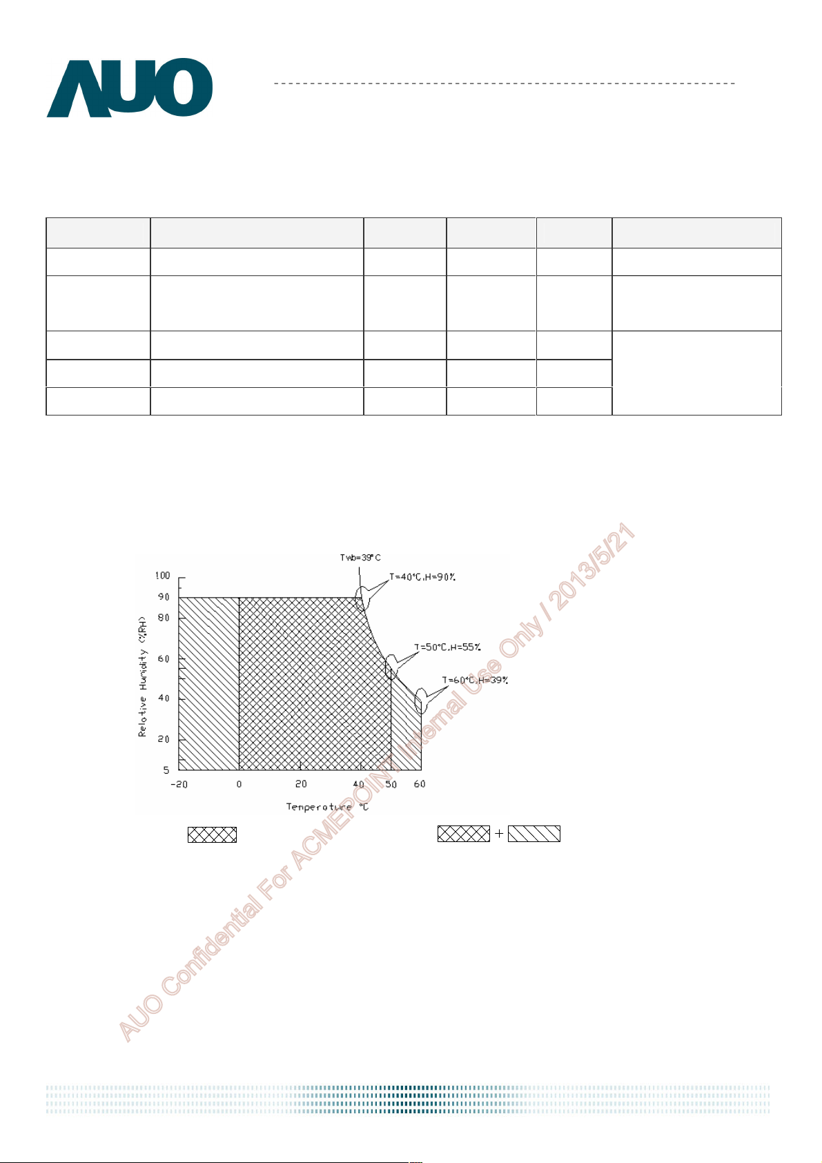
Note 2-1: Temperature and relative humidity range are shown as the below figure.
1. 90% RH Max ( Ta ≦39℃)
2. Max wet-bulb temperature at 39℃ or less. ( Ta ≦39℃)
3. No condensation
Note 2-1
Note 2-1
Operating Range
Storage Range
AUO Confidential For ACMEPOINT Internal Use Only / 2013/5/21
document version 1.0 6
Page 7
Product Specification
AU OPTRONICS CORPORATION
2.3 Optical Characteristics
The optical characteristics are measured on the following test condition.
Test Condition:
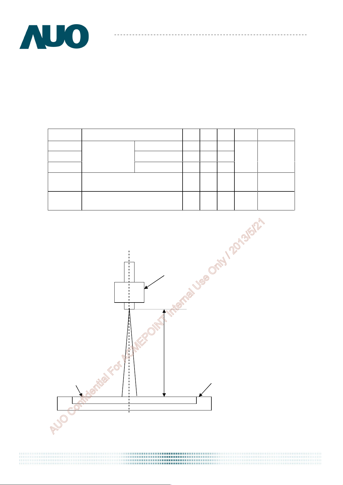
1. Equipment setup: Please refer to Note 2-2.
2. Panel Lighting time: 30 minutes
3. VDD=5.0V, Fv=60Hz,Is=65mA,Ta=25℃
M190PW01 V8
Symbol Description Min. Typ. Max. Unit Remark
TR
TF
Response Time
-
CT
FdB
Flicker (Center of screen) - -
Note 2-2: Equipment setup :
Rising Time - 3.8 5.5
Falling Time -
Rising + Falling
Crosstalk - -
1.2 2.5
-
Photo detector (SR-3, TRD-100)
5 8
1.5
-20
[msec]
[%]
[dB]
Note 2-3
By TRD-100
Note 2-4
By SR-3
Note 2-5
By SR-3
Measured distance (50cm)
Center of the screen
AUO Confidential For ACMEPOINT Internal Use Only / 2013/5/21
document version 1.0 7
Page 8
Product Specification
T
Black
1 Frame
T
AU OPTRONICS CORPORATION
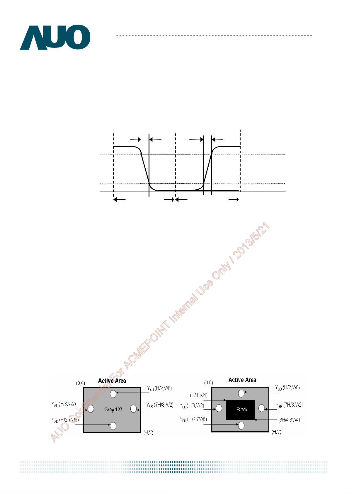
Note 2-3: Response time measurement
The output signals of photo detector are measured when the input signals are changed
from “Black” to “White” (rising time, TR), and from “White” to “Black” (falling time, TF),
respectively. The response time is interval between the 10% and 90% of optical
response. (Black & White color definition: Please refer section 3.4.3)
M190PW01 V8
Optica l
Optica l
resp on se
resp on se
10 0
10 0
90
10
10
%
%
White
0
0
Note 2-4: Crosstalk measurement
Definition:
CT = Max. (CTH,CTV);
Where
F
1 Frame
B lack
R
White
a.Maximum Horizontal Crosstalk :
CTH = Max. (| YBL – YAL | / YAL × 100 %, | YBR – YAR | / YAR × 100 %);
Maximum Vertical Crosstalk:
CTV = Max. (| YBU – YAU | / YAU × 100 %, | YBD – YAD | / YAD × 100 %);
b. YAU, YAD, YAL, YAR = Luminance of measured location without Black pattern
YBU, YBD, YBL, YBR = Luminance of measured location with Black pattern
AUO Confidential For ACMEPOINT Internal Use Only / 2013/5/21
document version 1.0 8
Page 9
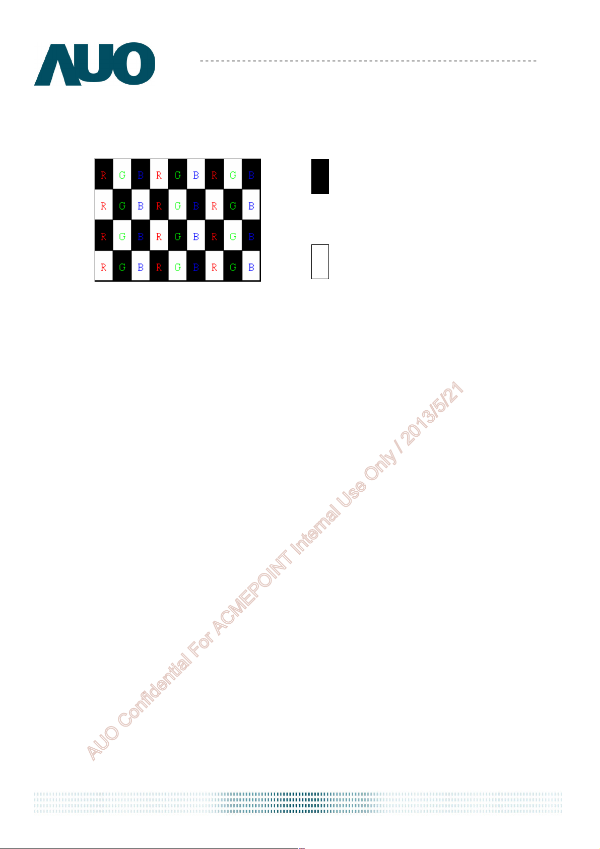
Note 2-5: Flicker measurement
a. Test pattern: It is listed as following.
Product Specification
AU OPTRONICS CORPORATION
Gray level = L0
Gray level = L127
M190PW01 V8
R: Red, G: Green, B:Blue
b. Measured position: Center of screen & perpendicular to the screen
AUO Confidential For ACMEPOINT Internal Use Only / 2013/5/21
document version 1.0 9
Page 10
Product Specification
VDD
AUO ASIC
Connec
tor
G
900
D
4320
X-Driver IC
AU OPTRONICS CORPORATION
M190PW01 V8
3 TFT-LCD Module
3.1 Block Diagram
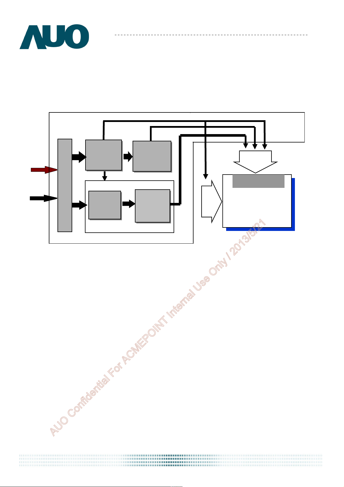
The following shows the block diagram of the 19.0 inch Color TFT-LCD Module.
LVDS
Signal
DC/DC
Converter
LVDS
Receiver
Control Board
Correction
ASIC
Gamma
Timing
Controller
Mini LVDS
Transmitter
D1
G1
TFT-LCD
1440(x3) x 900
Pixels
document version 1.0 10
AUO Confidential For ACMEPOINT Internal Use Only / 2013/5/21
Page 11
Product Specification
1 RxO0
- Negative LVDS differential data input (Odd data)
2 RxO0+
Positive LVDS differential data input (Odd data)
3 RxO1
- Negative LVDS differential data input (Odd data)
4 RxO1+
Positive LVDS differential data input (Odd data)
5 RxO2
- Nega
tive LVDS differential data input (Odd data)
6 RxO2+
Positive LVDS differential data input (Odd data)
7 GND
Ground
8 RxOCLK
- Negative LVDS differential clock input (Odd clock)
9 RxOCLK+
Positive LVDS differential clock input (Odd clock)
10 RxO3
- Negative LVDS differential data input (Odd data)
11 RxO3+
Positive LVDS differential data input (Odd data)
12 RxE0
- Negative LVDS differential data input (Even data)
13 RxE0+
Positive LVDS differential data input (Even data)
14 GND
Ground
15 RxE1
- Negative LVDS differential data input (Even data)
16 RxE1+
Positive LVDS differential data input (Even data)
17 GND
Ground
18 RxE2
- Negative LVDS differential data input (Even data)
19 RxE2+
Positive LVDS differential data input (Even data)
20 RxECLK
- Negative LVDS differential clock input (Even clock)
21 RxECLK+
Positive LVDS differential clock input (Even clock)
22 RxE3
- Negative LVDS differential data input (Even data)
23 RxE3+
Positive LVDS differential data input (Even data)
AU OPTRONICS CORPORATION
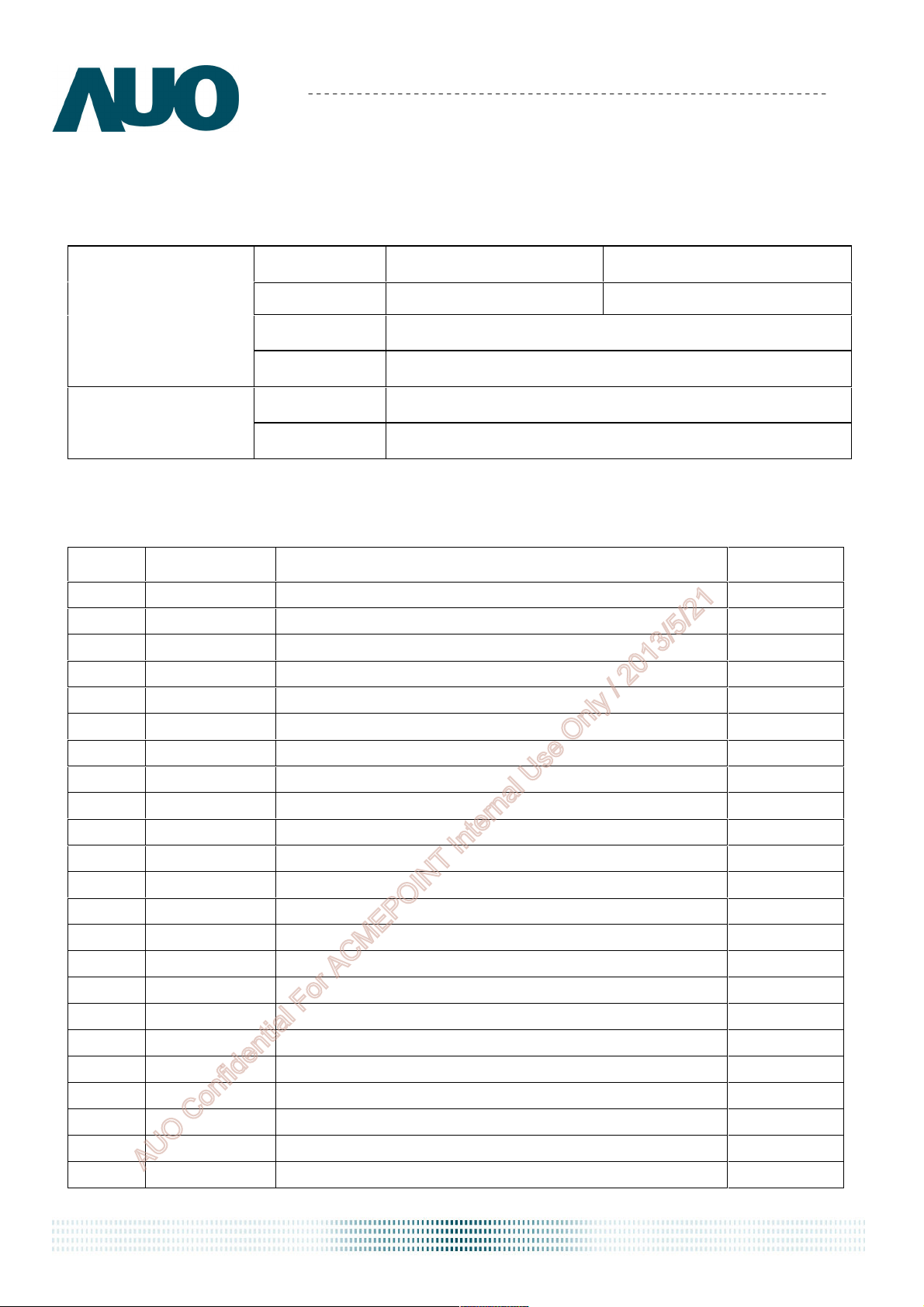
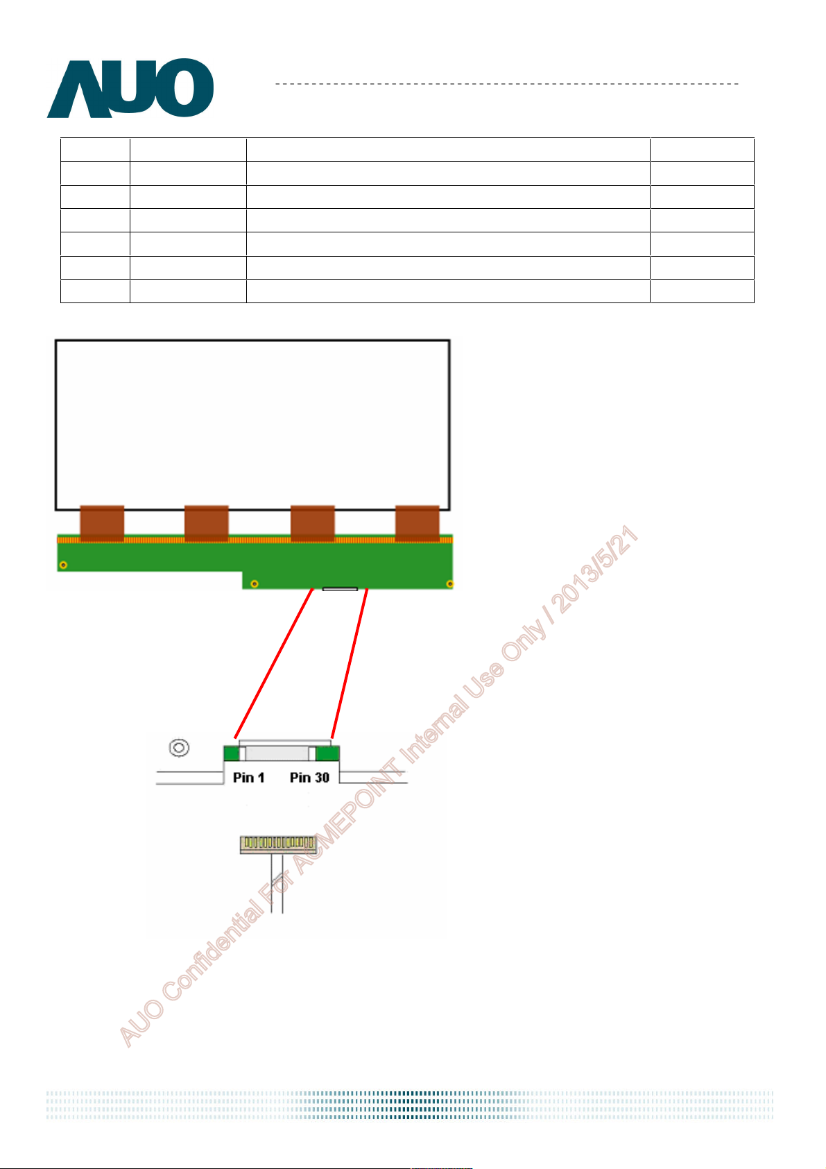
3.2 Interface Connection
3.2.1 Connector Type
TFT-LCD Connector
Mating Connector
3.2.2 Connector Pin Assignment
Manufacturer STM JAE
Part Number MSCK2407P30 FI-XPB30SR2A-HF11
Manufacturer STARCONN
Part Number 093F30-B0T01A
Manufacturer JAE
Part Number FI-X30HL-T ( Locked Type )
M190PW01 V8
PIN # Symbol Description Remark
AUO Confidential For ACMEPOINT Internal Use Only / 2013/5/21
document version 1.0 11
Page 12
Product Specification
24 GND
Ground
25 NC No connection (for AUO test only. Do not connect)
26 NC No connection (for AUO test only. Do not connect)
27 NC No connection (for AUO test only. Do not connect)
28 VDD
Power Supply Input Voltage
29 VDD
Power Supply Input Voltage
30
VDD
Power Supply Input Voltage
AU OPTRONICS CORPORATION
M190PW01 V8
AUO Confidential For ACMEPOINT Internal Use Only / 2013/5/21
document version 1.0 12
Page 13
Product Specification
AU OPTRONICS CORPORATION
3.3 Electrical Characteristics
3.3.1 Absolute Maximum Rating
Permanent damage may occur if exceeding the following maximum rating.
M190PW01 V8
Symbol
VDD
Description Min Max Unit
Power Supply
Input Voltage
GND-0.3 6.0 [Volt]
3.3.2 Recommended Operating Condition
Symbol
VDD
IDD
PDD
IRush Inrush Current
VDDrp
Description Min Typ Max Unit
Power supply
Input voltage
Power supply
Input Current (RMS)
VDD Power
Consumption
Allowable VDD
Ripple Voltage
4.5 5.0 5.5 [Volt]
- 0.9 1.1
1.1 1.4
- 4.5 5.5
5.5 7.0
-
-
- 3.0 [A] Note 3-1
- 500 [mV]
[A]
[A]
[Watt]
[Watt]
Remark
Ta=25℃
Remark
VDD= 5.0V, Black Pattern, Fv=60Hz
VDD= 5.0V, Black Pattern, Fv=75Hz
VDD= 5.0V, Black Pattern, Fv=60Hz
VDD= 5.0V, Black Pattern, Fv=75Hz
VDD= 5.0V, Black Pattern, Fv=75Hz
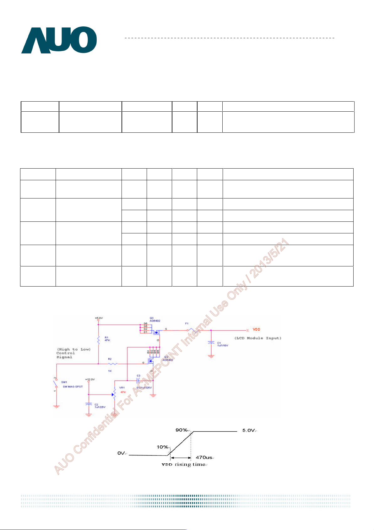
Note 3-1: Inrush Current measurement:
Test circuit:
AUO Confidential For ACMEPOINT Internal Use Only / 2013/5/21
The duration of VDD rising time: 470us.
document version 1.0 13
Page 14
R G B R G B
R G B R G B
R G B R G B
R G B R G B
1 2 1439
1440
1st Line
900
Line
3.4 Signal Characteristics
3.4.1 LCD Pixel Format
Product Specification
AU OPTRONICS CORPORATION
M190PW01 V8
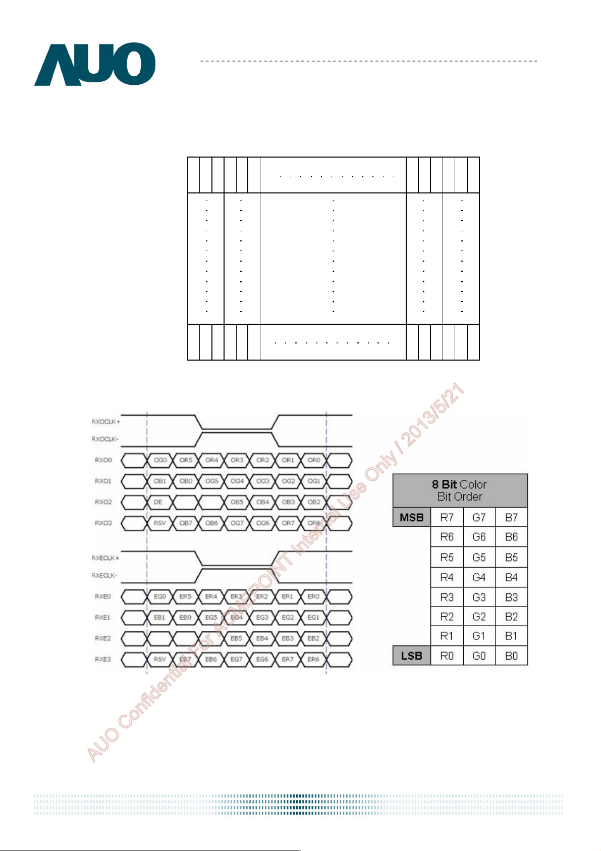
3.4.2 LVDS Data Format
Note 3-2:
a. O = “Odd Pixel Data” E = “Even Pixel Data”
b. Refer to 3.4.1 LCD pixel format, the 1st data is 1 (Odd Pixel Data), the 2nd data is 2 (Even Pixel Data) and the
last data is 1440 (Even Pixel Data).
AUO Confidential For ACMEPOINT Internal Use Only / 2013/5/21
document version 1.0 14
Page 15
Product Specification
M190PW01 V8
AU OPTRONICS CORPORATION
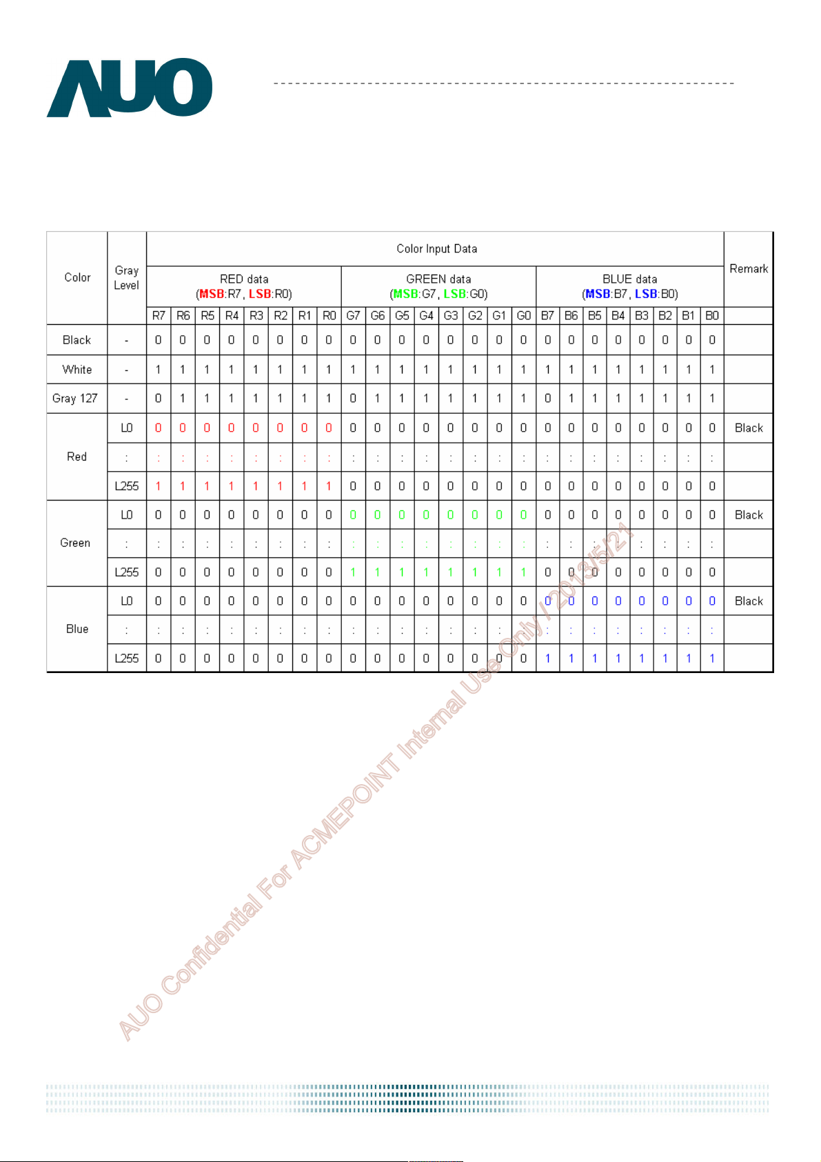
3.4.3 Color versus Input Data
The following table is for color versus input data (8bit). The higher the gray level, the brighter
the color.
AUO Confidential For ACMEPOINT Internal Use Only / 2013/5/21
document version 1.0 15
Page 16
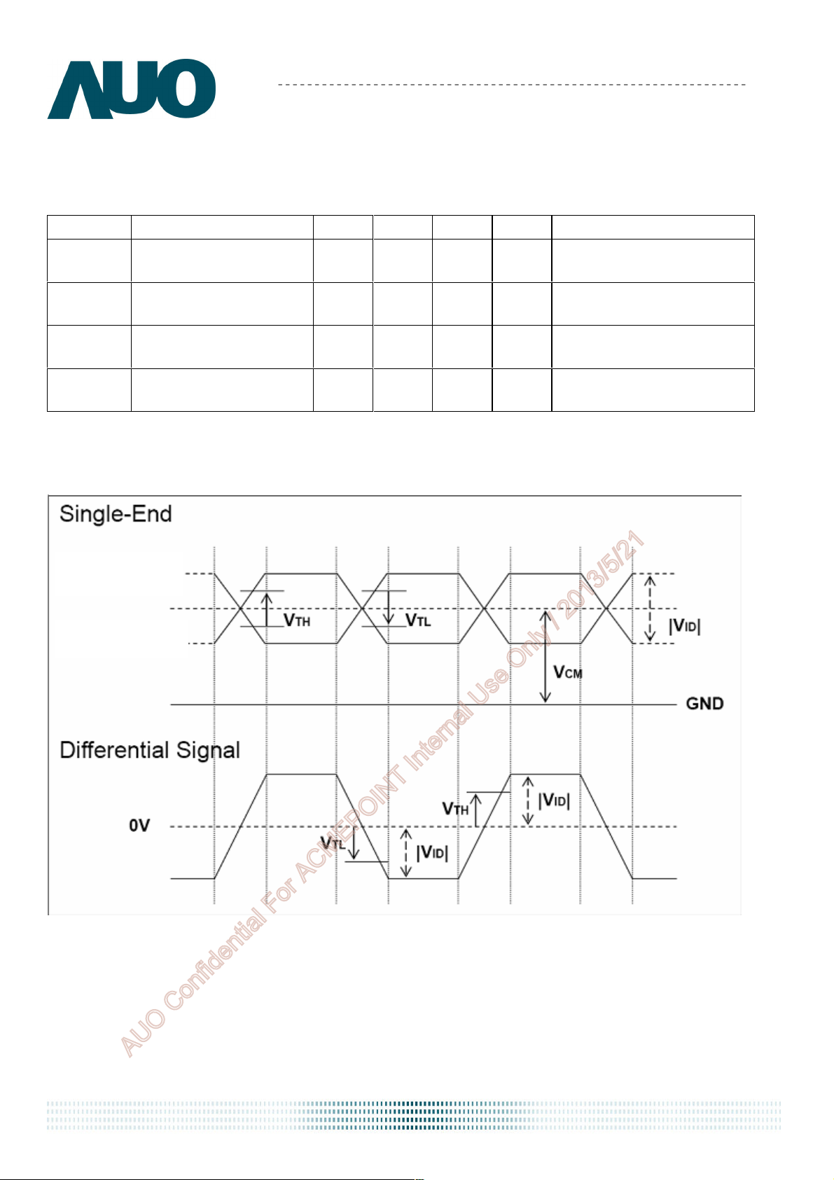
3.4.4 LVDS Specification
a. DC Characteristics:
Product Specification
AU OPTRONICS CORPORATION
M190PW01 V8
Symbol
VTH
VTL
│VID│
VCM
Description Min Typ Max Units
LVDS Differential
Input High Threshold
LVDS Differential
Input Low Threshold
LVDS Differential
Input Voltage
LVDS Common Mode
Voltage
-100
100 - 600 [mV]
+1.0 +1.2 +1.5 [V] VTH-VTL = 200mV
LVDS Signal Waveform:
Use RxOCLK- & RxOCLK+ as example.
RxOCLK-
Condition
- - +100 [mV] VCM = 1.2V
- - [mV] VCM = 1.2V
RxOCLK+
AUO Confidential For ACMEPOINT Internal Use Only / 2013/5/21
document version 1.0 16
Page 17
Product Specification
Freq
F
max
F
clk
F
min
F
clk
* F
DEV
< Spread Spectrum>
T
ime
AU OPTRONICS CORPORATION
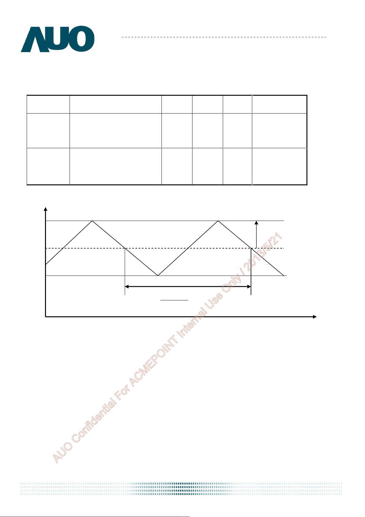
b. AC Characteristics:
Symbol Description Min Max Unit Remark
Maximum deviation of
M190PW01 V8
F
DEV
input clock frequency
-
± 3 %
during Spread Spectrum
Maximum modulation
F
MOD
frequency of input clock
-
200 KHz
during Spread Spectrum
1
FMOD
Fclk: LVDS Clock Frequency
AUO Confidential For ACMEPOINT Internal Use Only / 2013/5/21
document version 1.0 17
Page 18
Product Specification
AU OPTRONICS CORPORATION
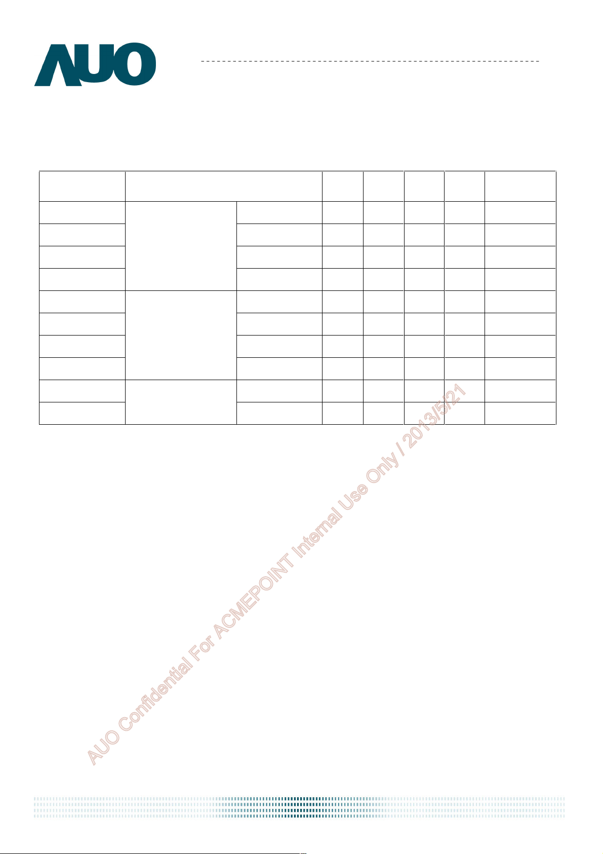
3.4.5 Input Timing Specification
It only support DE mode, and the input timing are shown as the following table.
M190PW01 V8
Symbol Description Min. Typ. Max. Unit
Tv Period
Tdisp (v) Active
Vertical Section
Tblk (v) Blanking
Fv
Frequency
Th Period
Tdisp (h) Active
Horizontal Section
Tblk (h) Blanking
Fh
Frequency 37.1 53.0 67.1 KHz Note 3-3
Tclk Period
LVDS Clock
Fclk
Frequency
912 916 1651
900 900 900
12 16 751
50 60 76
813 964 1472
720 720 720
93 244 752
50 60 76
45.6
55.0 82.5
Th
Th
Th
Hz
Tclk
Tclk
Tclk
ns 1/Fclk
MHz Note 3-4
Remark
Note 3-3: The equation is listed as following. Please don’t exceed the above recommended value.
Fh (Min.) = Fclk (Min.) / Th (Min.);
Fh (Typ.) = Fclk (Typ.) / Th (Typ.);
Fh (Max.)= Fclk (Max.) / Th (Min.);
Note 3-4: The equation is listed as following. Please don’t exceed the above recommended value.
Fclk (Min.) = Fv (Min.) x Th (Min.) x Tv (Min.);
Fclk (Typ.) = Fv (Typ.) x Th (Typ.) x Tv (Typ.);
Fclk (Max.) = Fv (Max.) x Th (Typ.) x Tv (Typ.);
AUO Confidential For ACMEPOINT Internal Use Only / 2013/5/21
document version 1.0 18
Page 19
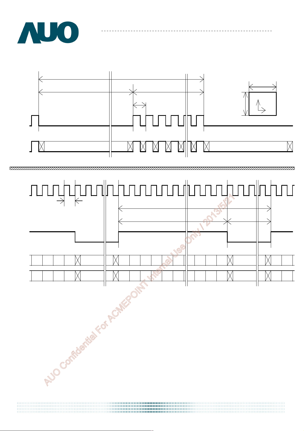
3.4.6 Input Timing Diagram
DE
RGB Data
CLK
DE
RGB Data
(Odd)
RGB Data
(Even)
N
Line
Pixel
M-7
Pixel
M-6
Pixel
M-5
Pixel
Pixel
M-3
Pixel
M-2
Tblk(v)
Invalid Data
Tclk
Pixel
M-1
Pixel
M
Invalid Data
Invalid Data
Product Specification
AU OPTRONICS CORPORATION
Tv
Tdisp(v)
Th
32
LineLine
Th
Tdisp(h)
Pixel
Pixel
10
4
LineLine
Pixel
Pixel
119
Pixel
12
1
Pixel
1
Pixel Pixel
2
Pixel
Pixel
3
4
Pixel
7
5
Pixel
Pixel
8 M
6 M-2
N
Line
M-5
M-4
Pixel
Pixel
M-3
M190PW01 V8
Invalid Data
Tblk(h)
Pixel
M-1
PixelPixel
Invalid Data
Invalid Data
N Line
M pixel
Y
X
Pixel
Pixel
1
3
Pixel
Pixel
2M-4
4
AUO Confidential For ACMEPOINT Internal Use Only / 2013/5/21
document version 1.0 19
Page 20
Product Specification
DATA
10%
90%
10%
90%
AU OPTRONICS CORPORATION
M190PW01 V8
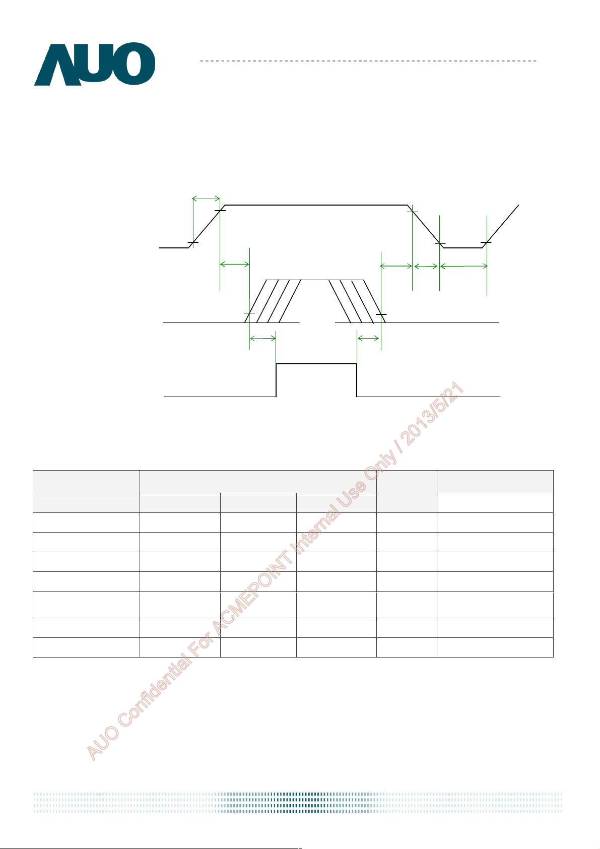
3.5 Power ON/OFF Sequence
VDD power,LVDS signal and backlight on/off sequence are as following. LVDS signals
from any system shall be Hi-Z state when VDD is off.
T1
VDD
LVDS Signal
Backlight Enable
Signal (system)
Symbol
T1 0.5 - 10 [ms]
T2 0 - 50 [ms]
T2
VALID
T3
Backlight Off
Power Sequence Timing
Backlight On
Value Remark
Min. Typ. Max.
T5
T4
Backlight Off
Unit
T6
T7
T3 500 - - [ms]
T4 100 - - [ms]
T5 0 50 [ms]
T6 0 - 150 [ms] Note 3-6
T7 1000 - - [ms]
Note 3-5
Note 3-6
Note 3-5 : Recommend setting T5 = 0ms to avoid electronic noise when VDD is off.
Note 3-6 : During T5 and T6 period , please keep the level of input LVDS signals with Hi-Z state.
AUO Confidential For ACMEPOINT Internal Use Only / 2013/5/21
document version 1.0 20
Page 21
Product Specification
KV, 150pF(330Ω ) 1sec,
AU OPTRONICS CORPORATION
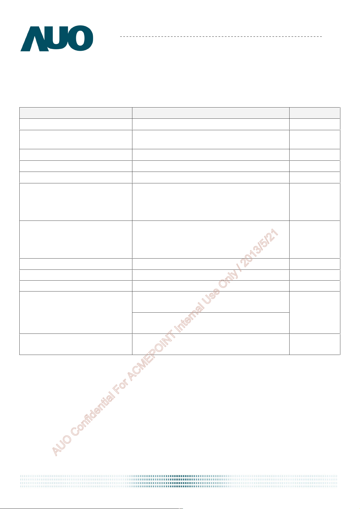
4 Reliability Test
AUO reliability test items are listed as following table. (Bare Panel only)
Items Condition
Temperature Humidity Bias (THB)
Ta= 50℃, 80%RH, 300hours
M190PW01 V8
Remark
High Temperature Operation (HTO)
Low Temperature Operation (LTO)
High Temperature Storage (HTS)
Low Temperature Storage (LTS)
Vibration Test
(Non-operation)
Shock Test
(Non-operation)
Drop Test Height: 60 cm, package test
Thermal Shock Test (TST)
On/Off Test On/10sec, Off/10sec, 30,000 cycles
ESD (Electro Static Discharge)
Ta= 50℃, 50%RH, 300hours
Ta= 0℃, 300hours
Ta= 60℃, 300hours
Ta= -20℃, 300hours
Acceleration: 1.5 Grms
Wave: Random
Frequency: 10 - 200 Hz
Sweep: 30 Minutes each Axis (X, Y, Z)
Acceleration: 50 G
Wave: Half-sine
Active Time: 20 ms
Direction: ±X, ±Y, ±Z (one time for each Axis)
-20℃/30min, 60℃/30min, 100 cycles Note 4-1
Contact Discharge: ± 15
8 points, 25 times/ point.
Air Discharge: ± 15KV, 150pF(330Ω ) 1sec
8 points, 25 times/ point.
Note 4-2
Altitude Test
Note 4-1: a. A cycle of rapid temperature change consists of varying the temperature from -20 to ℃
60 , and back again. Power is not applied during the test. ℃
b. After finish temperature cycling, the unit is placed in normal room ambient for at least 4
hours before power on.
Note 4-2: EN61000-4-2, ESD class B: Certain performance degradation allowed
AUO Confidential For ACMEPOINT Internal Use Only / 2013/5/21
document version 1.0 21
Operation:18,000 ft
Non-Operation:40,000 ft
No data lost
Self-recoverable
No hardware failures.
Page 22
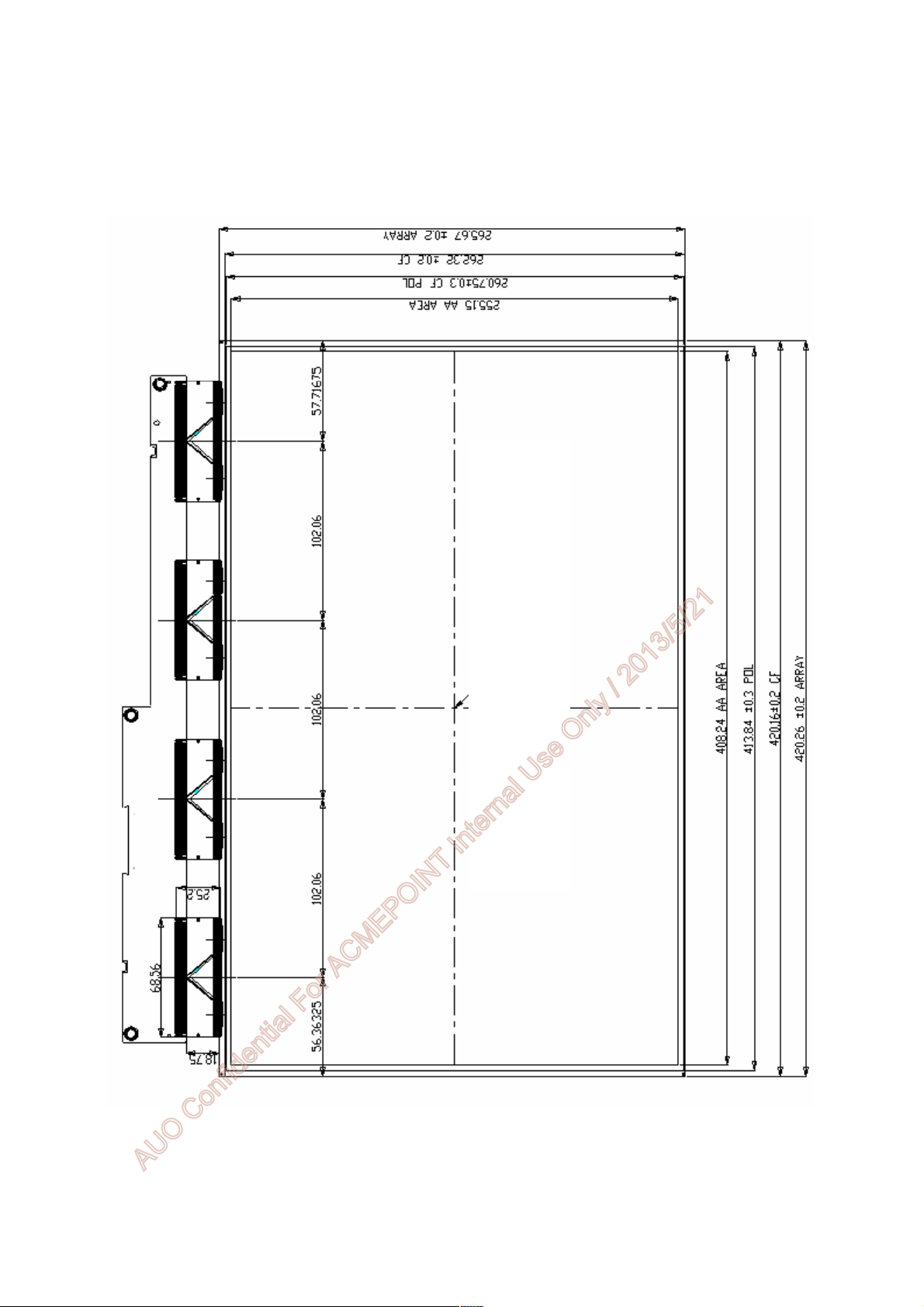
Ver 1.2
Avoid touching COF position when
doing mechanical design
AUO Confidential For ACMEPOINT Internal Use Only / 2013/5/21
5 Mechanical Characteristic
 Loading...