

Page 1
Global LCD Panel Exchange Center
www.fpdclub.net
www.panelook.com
M190EN03 V.3
Product Specification
AU OPTRONICS CORPORAT
ION
Product Specification
19.0” SXGA Color TFT-LCD Module
Model Name: M190EN03 V.3
Approved by
CC Chiu
Prepared by
Belinda Chen
DDBU Marketing Division / AU Optronics corporation
Customer Checked & Approved by
Ve
r0.4 1/28
One step solution for LCD / PDP / OLED panel application: Datasheet, inventory and accessory!
www.panelook.com
Page 2

Global LCD Panel Exchange Center
www.panelook.com
Product Specification
Product S
M190EN03 V.3
p
ecification
19.0” SXGA Color TFT
-LCD Module
Model Name: M190EN03
V.3
() Preliminary
( ) Final Specifications
Note: This Specification is subject to change without notice.
Specifications
Ve
r0.4 2/28
One step solution for LCD / PDP / OLED panel application: Datasheet, inventory and accessory!
www.panelook.com
Page 3

Global LCD Panel Exchange Center
www.panelook.com
M190EN03 V.3
Product Specification
Contents
1.0 Handling Precautions.............................................................6
2.0 General Description ...............................................................8
2.1 Display Characteristics.......................................................................................................
2.2 Optical Characteristics ....................................................................................................... 9
3.0 Functional Block Diagram ....................................................
4.0 Absolute Maximum Ratings..................................................
4.1 TFT
4.2 Backlight Unit ................................................................................................................... 13
4.3 Absolute Ratings of Environment ..................................................................................... 13
5.0 Electrical characteristics
5.1 TFT
5.1.1 Power Specification .............................................................................................. 14
5.1.2 Signal Electrical Characteristics ....................................................................................
5.2 Backlight Unit ................................................................................................................... 16
LCD Module.............................................................................................................. 13
......................................................
LCD Module.............................................................................................................. 14
6.0 Signal Characteristic ............................................................
6.1 Pixel Format Image
6.2 The Input Data Format ..................................................................................................... 17
6.3 Signal Description ............................................................................................................ 18
6.4.1 Timi
ng Characteristics .......................................................................................... 20
.......................................................................................................... 17
8
12
13
14
15
17
6.4.2 Timi
6.5 Power ON/OFF Sequence ............................................................................................... 21
ng diagram ................................................................................................... 20
7.0 Connector & Pin Assignment................................................22
7.1 TFT
7.2 Backlight Unit ................................................................................................................... 23
7.3 Signal for Lamp Connector .............................................................................................. 23
8.0 Vibration, Shock, and Drop ..................................................
8.1 Vi
8.2 Drop Test.......................................................................................................................... 24
LCD Module.............................................................................................................. 22
23
bration & Shock............................................................................................................. 23
9.0 Environment ........................................................................24
9.1 Te
9.2 Atmospheric Pressure ......................................................................................................
9.3Thermal Shock ..................................................................................................................24
10.0 Reliability...........................................................................
10.1 Failure Criteria................................................................................................................
mperature and Humidity ............................................................................................... 24
9.1.1 Operatin
9.1.2 Shipping Conditions ............................................................................................. 24
g Conditions............................................................................................ 24
24
25
25
10.2 Failure Rate.................................................................................................................... 25
Ve
r0.4 3/28
One step solution for LCD / PDP / OLED panel application: Datasheet, inventory and accessory!
www.panelook.com
Page 4

Global LCD Panel Exchange Center
www.panelook.com
M190EN03 V.3
Product Specification
10.2.1 Usage ..............................................................................................................
10.2.1 Component De-rating ......................................................................................... 25
10.3 On/OFF Cycle ................................................................................................................
11.0 Safety ................................................................................
.1 Sharp Edge Requirements ............................................................................................. 26
11
25
25
26
11.2 Materials......................................................................................................................... 26
11.2.1 Toxicity
11.2.2 Flammability ..................................................................................................... 26
.3 Capacitors ...................................................................................................................... 26
11
............................................................................................................ 26
12.0 Other requirement .............................................................26
12.1 National T
12.2 Label .............................................................................................................................. 26
13.0 Mechanical Characteristics.................................................
est Lab Requirement ...................................................................................... 26
27
Ve
r0.4 4/28
One step solution for LCD / PDP / OLED panel application: Datasheet, inventory and accessory!
www.panelook.com
Page 5
Global LCD Panel Exchange Center
R
R
e
e
R
R
www.panelook.com
M190EN03 V.3
Product Specification
Record of Revision
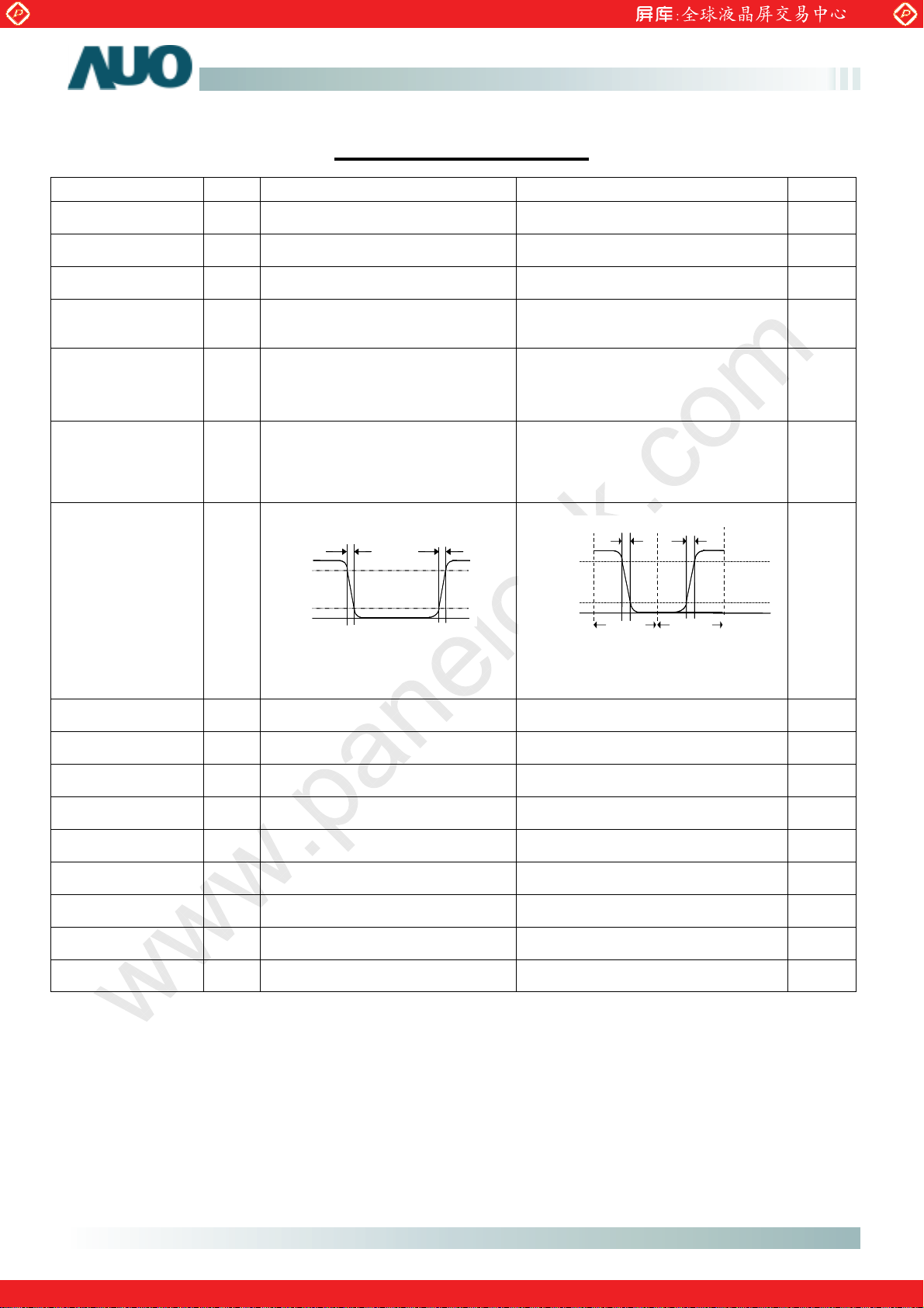
Version and Date Page Old description New Description Remark
0.1 2005/03/14 All
First Edition for Customer All
0.2 2005/05/12 8
N/A RoHS Compliance
9 Contrast Ratio:Min:500 Contrast Ratio:Min:750
0.3 2005/07/28 8 Optical Response Time:
20ms (Typ, on/off)
9 Response Time:
Rising Time:15 ms
Rising + Falling:20 ms
9
The response time is interval
between the 10% and 90% of
amplitudes.
0.4 2005/07/28 9
%
%
Tr
Tr
F
F
100
100
90
90
tical
tical
Op
Op
response
response
i
i
te Black White
te Black White
Wh
Wh
10
10
0
0
Tr
Tr
Optical Response Time:
14ms (Typ, on/off)
Response Time:
Rising Time:9
Rising + Falling: 14 ms
The response time is interval between
the 10% and 83% (1 frame at 60 Hz)
of amplitudes.
%
%
Tr
Tr
F
F
100
100
90
Op
Op
tical
tical
response
response
10
10
0
0
te Black
Whi
Bla
1 Fra
m
ck
The response time is interval
between the 10% and 83% (1 frame
at 60 Hz) of amplitudes.
The response time is interval between
the 10% and 90% (1 frame at 60 Hz)
of amplitudes.
Added
Revised
Revised
Revised
Rev
sed
i
Tr
Tr
te
Whi
Revised
1 Fr
am
Ve
r0.4 5/28
One step solution for LCD / PDP / OLED panel application: Datasheet, inventory and accessory!
www.panelook.com
Page 6

Global LCD Panel Exchange Center
www.panelook.com
M190EN03 V.3
Product Specification
1.0 Handling Precautions
1) Since front polarizer is easily damaged, pay attention not to scratch it.
2) Be sure to turn off power supply when inserting or disconnecting from input connector.
3) Wipe off water drop immediately. Long contact with water may cause discoloration or spots.
4) When the panel surface is soiled, wipe it with absorbent cotton or other soft cloth.
5) Since the panel is made of glass, it may break or crack if dropped or bumped on hard surface.
6) Since CMOS LSI is used in this module, take care of static electricity and insure human earth when
handling.
7) Do not open nor modify the Module Assembly.
8) Do not press the reflector sheet at the back of the module to any directions.
9) In case if a module has to be put back into the packing container slot after once it was taken out from
the container, do not press the center of the CCFL reflector edge. Instead, press at the far ends of the
CCFL reflector edge softly. Otherwise the TFT module may be damaged.
10) At the insertion or removal of the Signal Interface Connector, be sure not to rotate nor tilt the Interface
Connector of the TFT module.
11) After installation of the TFT module into an enclosure (Desktop monitor Bezel, for example), do not twist
nor bend the TFT Module even momentary. At designing the enclosure, it should be taken into
consideration that no bending/twisting forces are applied to the TFT module from outside. Otherwise
the TFT module may be damaged.
Ve
r0.4 6/28
One step solution for LCD / PDP / OLED panel application: Datasheet, inventory and accessory!
www.panelook.com
Page 7
Global LCD Panel Exchange Center
www.panelook.com
Product Specification
2.0 General Description
This specification applies to the 19.0 inch Color TFT-LCD Module M190EN03 V3.
The display supports the SXGA (1280(H) x 1024(V)) screen format and 16.7M colors (RGB 8-bits data).
All input signals are 2 Channel LVDS interface compatible.
This module does not contain an inverter card for backlight.
2.1 Display Characteristics
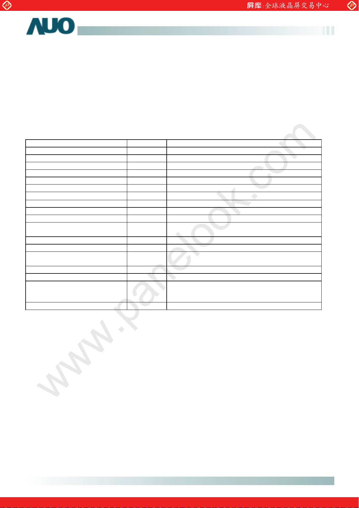
The following items are characteristics summary on the table under 25 к condition:
ITEMS Unit SPECIFICATIONS
Screen Diagonal [mm]
Active Area [mm]
Pixels H x V 1280(x3) x 1024
Pixel Pitch [mm] 0.294 (per one triad) x 0.294
Pixel Arrangement
Display Mode Normally Black
White Luminance ( Center ) [cd/m2]
Contrast Ratio 1,000 : 1 (Typ)
Optical Response Time [msec]
Nominal Input Voltage VDD [Volt] +5.0 V
Power Consumption
(VDD line + CCFL line)
Weight [Grams] 2500 (Max)
Physical Size [mm]
Electrical Interface Even/Odd R/G/B data, 3 sync signal,
Support Color 16.7M colors (RGB 8-bit data )
Surface treatment Anti-glare, hard coating (3H)
Temperature Range
Operating
Storage
RoHS RoHS Compliance
(Shipping)
[Watt]
o
C]
[
o
C]
[
480(19")
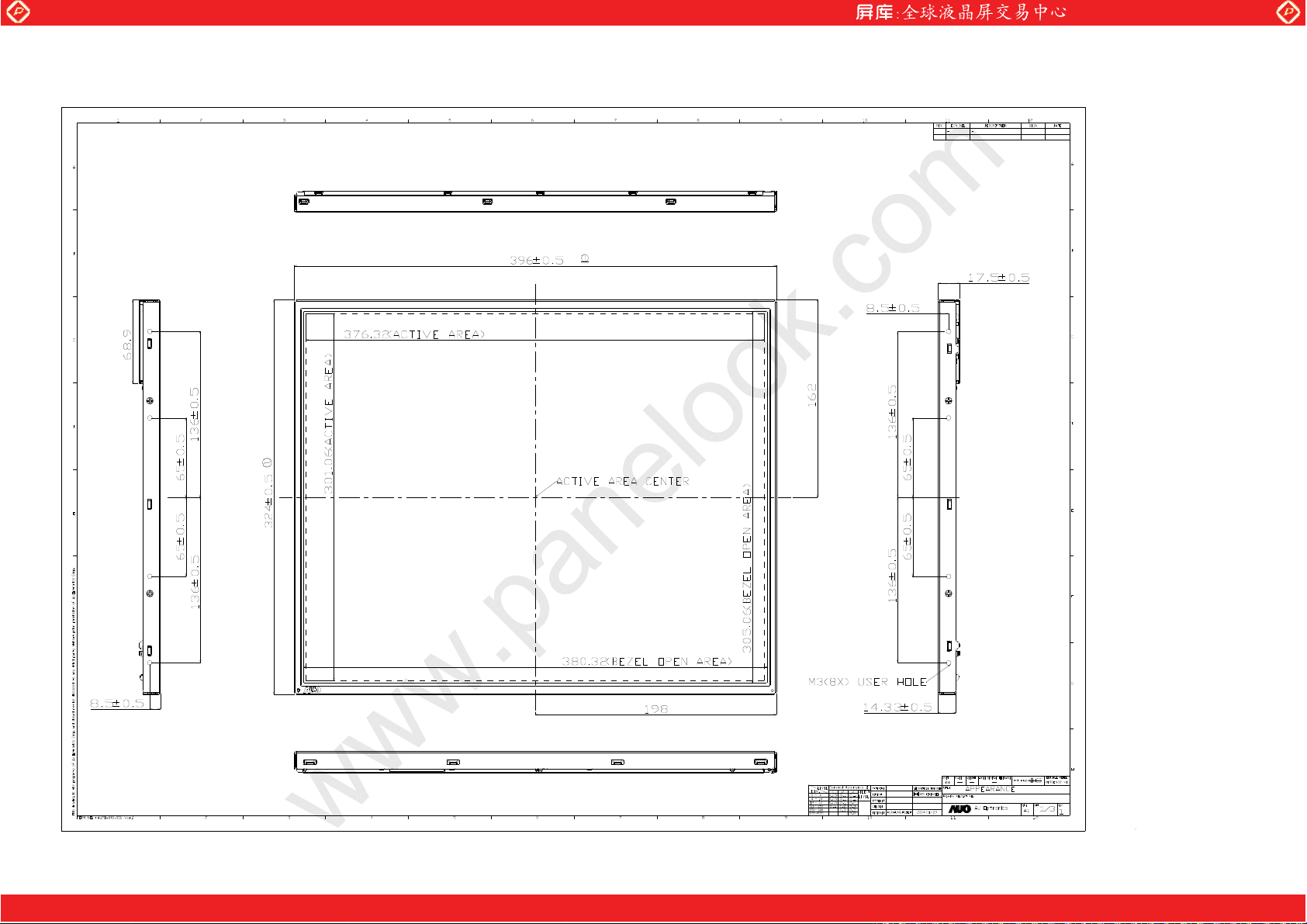
376.32 (H) x 301.056 (V)
R.G.B. Vertical Stripe
250 cd/m
14 ms (Typ, on/off)
27.5W(Typ) (w/o Inverter, All white pattern)
396(W) x 324(H) x 17.5(D) (Typ)
Clock
0 to +50
-20 to +60
2 @7mA
(Ty
p
)
M190EN03 V.3
Ve
r0.4 8/28
One step solution for LCD / PDP / OLED panel application: Datasheet, inventory and accessory!
www.panelook.com
Page 8
Global LCD Panel Exchange Center
www.panelook.com
Product Specification
2.2 Optical Characteristics
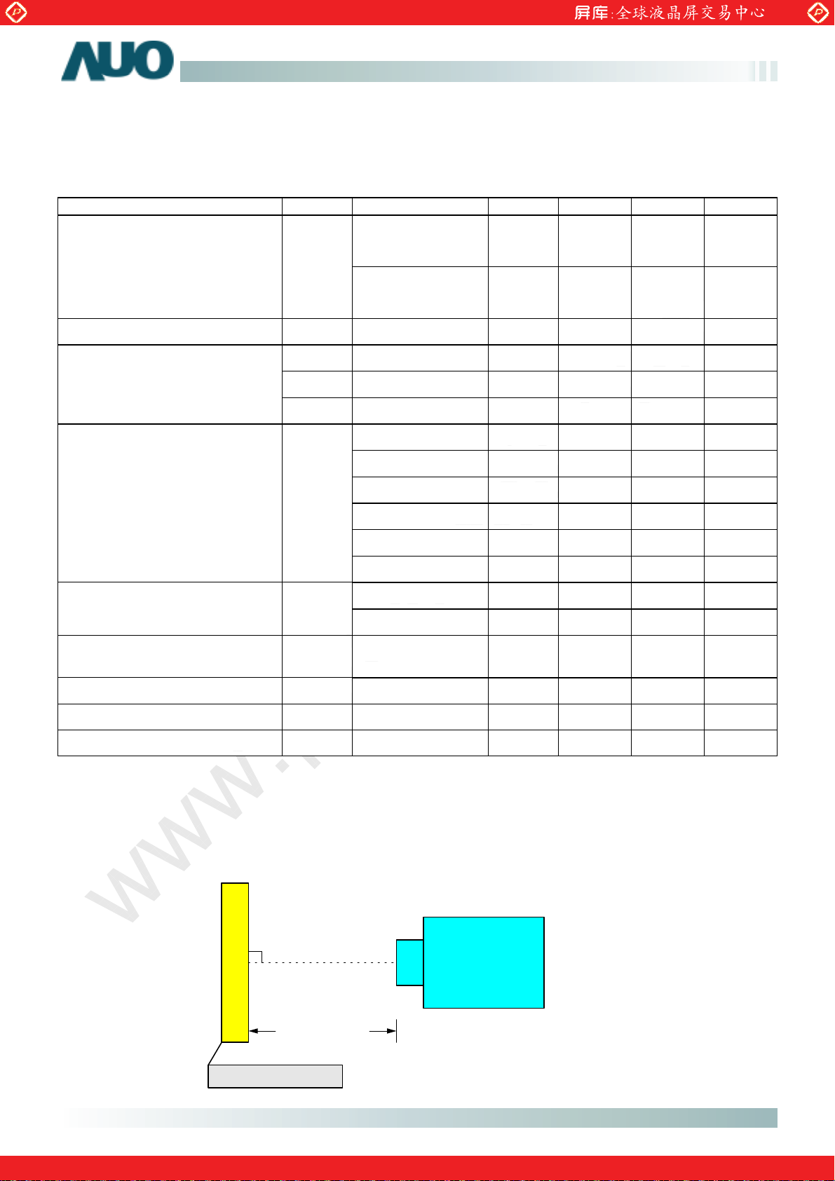
The optical characteristics are measured under stable conditions at 25к:
Item Unit Conditions Min. Typ. Max. Note
Viewing Angle
Contrast Ratio
Response Time
Color / Chromatici
Coordinates (CIE)
[degree]
[degree]
[degree]
[degree]
sec]
[m
[m
sec]
[msec] Rising + Falling - 14 40
ty
Horizontal (Right)
10 (Left)
CR =
Vertical (Up)
CR =
10 (Down)
Normal Direction 750 1,000
Rising Time - 9 25
Falling Time - 5 15
Red x 0.611 0.641 0.671
Red y 0.323 0.353 0.383
75
75
75
75
85
85
85
85
M190EN03 V.3
-
-
-
-
Note 1
Note 1
Note 1
Green x 0.259 0.289 0.319
Green y 0.596 0.626 0.656
Blue x 0.112 0.142 0.172
Blue y 0.048 0.078 0.108
Color Coordinates (CIE) White
White Luminance at CCFL 7.0mA
(central point)
Luminance Uniformity
Crosstalk (in75Hz)
Flicker
Equipment Pattern Generator, Power Supply, Digital Voltmeter, Luminance meter (PR 880, BM-5A /
BM7, CS-1000, CA210, SR_3, EZ Contrast*, Optiscope & Westar TRD-100)
Aperture
Test Point Center (VESA point 9)
Environment < 1 lux
1with 100cm VD or 2with 50cm viewing distance
[cd/m2] 200 250 -
[%] 75 80 -
[%] 1.5
dB -20
White x 0.283 0.313 0.343
White y 0.299 0.329 0.359
Note 2
Note 3
Note 4
LCD Module
PR-880 /
BM5A /
BM7
measuring distance
Module Driving Equipment
Ve
r0.4 9/28
One step solution for LCD / PDP / OLED panel application: Datasheet, inventory and accessory!
www.panelook.com
Page 9

Global LCD Panel Exchange Center
*’ EZ Contrast is different measurement tool with very close viewing distance.
Note 1: Definition of Response time
The output signals of photodetector are measured when the input signals are changed from “Full Black” to
www.panelook.com
M190EN03 V.3
Product Specification
“Full White” (rising time), and from “Full White” to “Full Black ”(falling time), respectively
interval between the 10% and 90% (1 frame at 60 Hz) of amplitudes.
%
Opt
Opt
ical
ical
response
response
10
10
90
10
10
%
0
0
Whi
0
0
Tr
Tr
F
F
te Black
1 Frame 1 Frame
Black
Tr
Tr
R
R
Whi
te
. The response time is
Note 2: Brightness uniformity of these 9 points is defined as below
90 %
50 %
Uniformity
10 %
10 %
50 %
90 %
9)-(1 points 9in Luminance Minimum
9)-(1 Points 9in Luminance Maximum
Ve
r0.4 10/28
One step solution for LCD / PDP / OLED panel application: Datasheet, inventory and accessory!
www.panelook.com
Page 10
Global LCD Panel Exchange Center
A
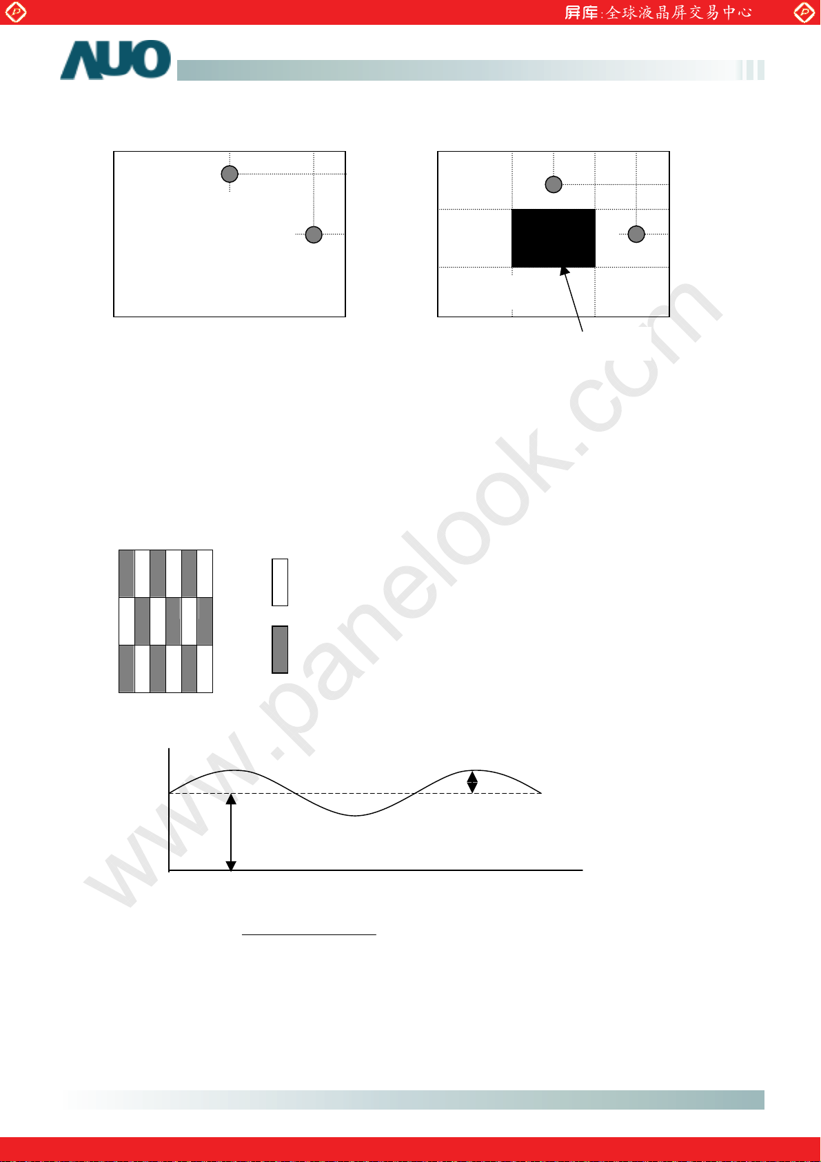
Note 3: Crosstalk is defined as below :
www.panelook.com
M190EN03 V.3
Product Specification
l
l
Note 4: Test
1/2
184 gray level 184 gray level
Unit: percentage of dimension of display area
l / LA x 100%= 1.5% max., LA and LB are brightness at location A and B
L
A-LA’
L
l / LB x 100%= 1.5% max., LA’ and LB’ are brightness at location A’ and B’
B-LB’
Paterm: Subchecker Pattern
1/6
1/6
1/2
B
2/3 1/3
A’
1/2
1/6
1/6
1/3
1/2
B’
2/3
0 gray level
R G B R G B
Gray Level = L127
R G B R G B
R G B R G B
Method: Record dBV & DC value with (WESTAR)TRD-100
Amplitude
DC
log20(dB)Flicker
Gray Level = L0
Hz) 30Level(at AC
Level DC
AC
Time
Ve
r0.4 11/28
One step solution for LCD / PDP / OLED panel application: Datasheet, inventory and accessory!
www.panelook.com
Page 11
Global LCD Panel Exchange Center
www.panelook.com
Product Specification
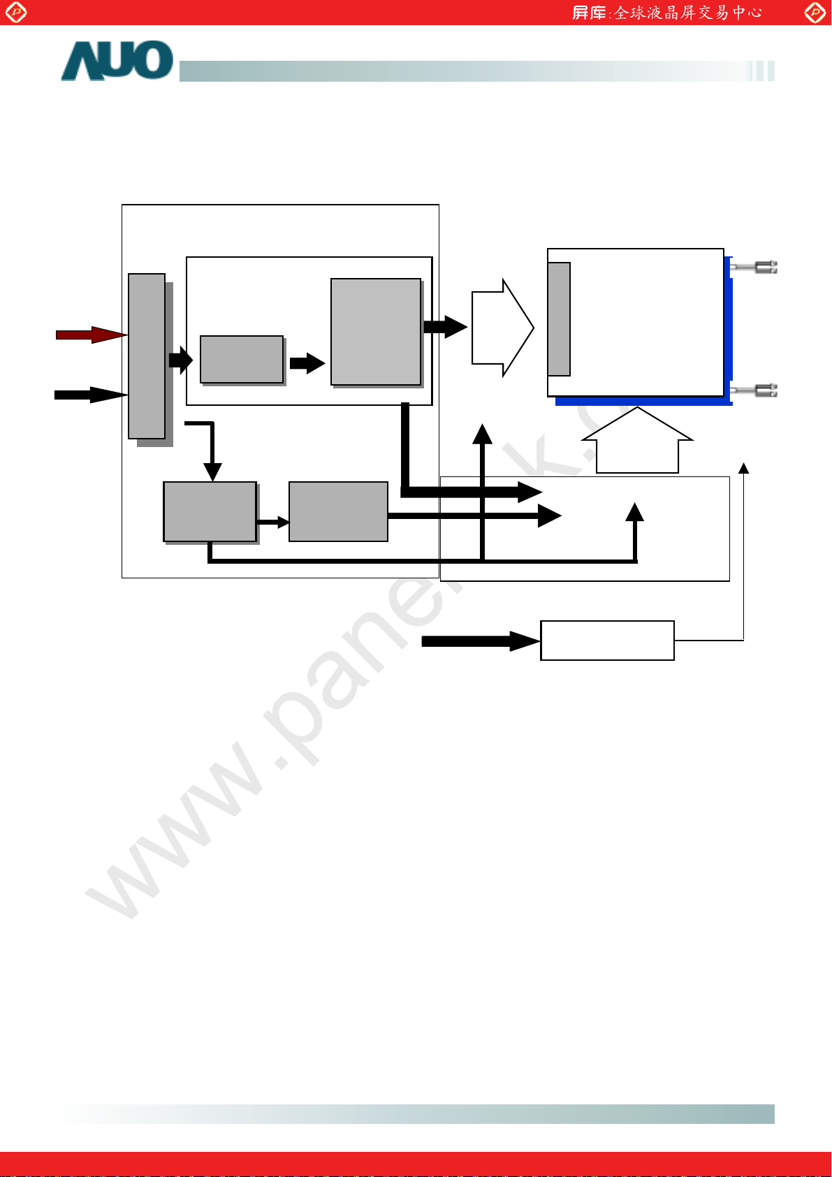
3.0 Functional Block Diagram
The following diagram shows the functional block of the 19.0 inches Color TFT/LCD Module:
M190EN03 V.3
Connector
LVDS
+
Receive
DC/DC
Converter
+
-
r
Gamma
Correction
Timing
Controller
G1024
-
D1 D3840
TFT-LCD
1280*(3)*1024
Pixels
-
4 CCFL
Inverter
ROSE MDF76KBW-30S-1H(58) JST BHSR-02VS-1
HI
Mating Type: Mating Type:
HIROSE MDF 76G-30P-1SD SM02B-BHSS-1-TB
Ve
r0.4 12/28
One step solution for LCD / PDP / OLED panel application: Datasheet, inventory and accessory!
www.panelook.com
Page 12
Global LCD Panel Exchange Center
4.0 Absolute Maximum Ratings
Absolute maximum ratings of the module is as following:
4.1 TFT LCD Module
www.panelook.com
M190EN03 V.3
Product Specification
Item Symbol
Logic/LCD Drive Voltage VIN -0.3 +5.5 [Volt] Note 1,2
Min Max Unit Conditions
4.2 Backlight Unit
Item Symbol Min Max Unit Conditions
CCFL Current ICFL - 7.5
[mA] rms Note 1,2
4.3 Absolute Ratings of Environment
Item Symbol Min Max Unit Conditions
Operating Humidity HOP 5 90 [%RH] Note 3
Storage Temperature TST -20 +60 [oC] Note 3
Storage Humidity HST 5 90 [%RH] Note 3
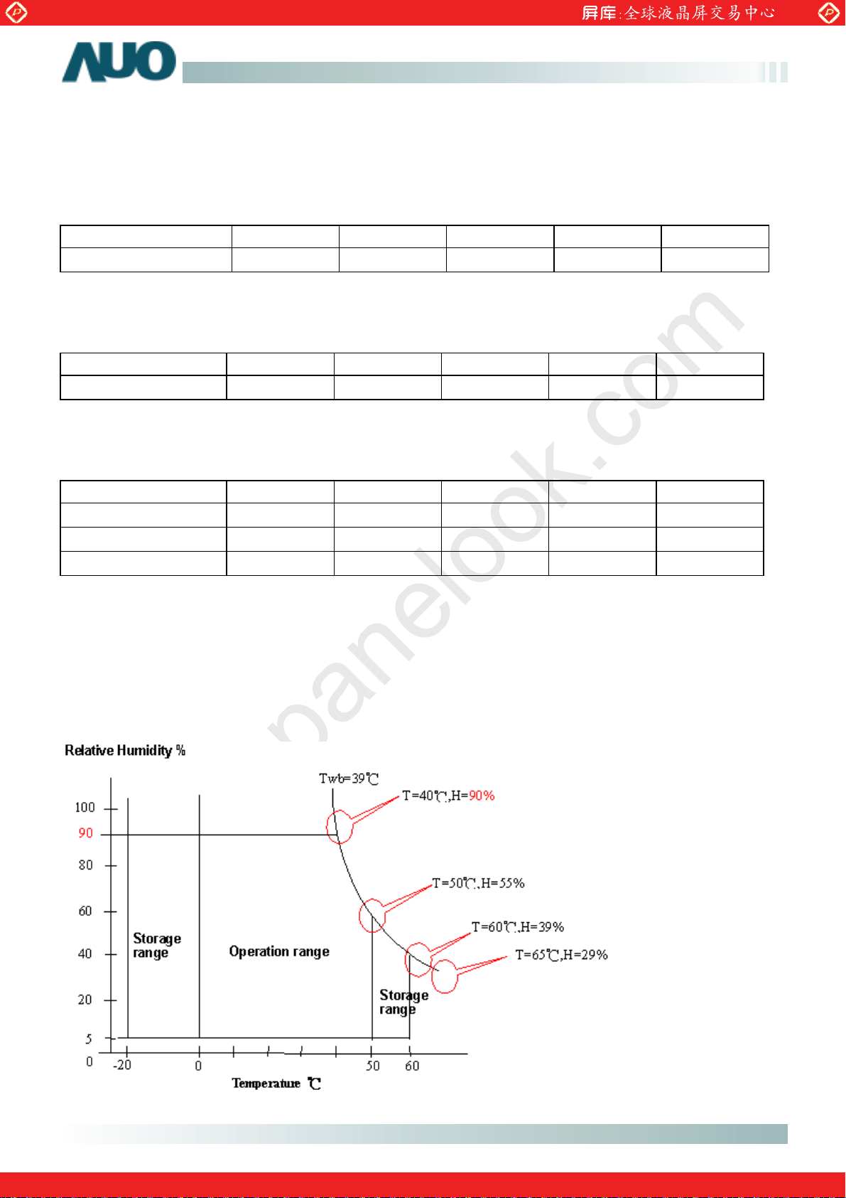
Please refer the graph below for corresponding of Min/Max values of temperature and humidity.
Note 1: With in Ta (25к )
Note 2: Permanent damage to the device may occur if exceed maximum values
Note 3: For quality perfermance, please refer to AUO IIS(Incoming Inspection Standard)
.
Ve
r0.4 13/28
One step solution for LCD / PDP / OLED panel application: Datasheet, inventory and accessory!
www.panelook.com
Page 13
Global LCD Panel Exchange Center
5.0 Electrical characteristics
5.1 TFT LCD Module
www.panelook.com
M190EN03 V.3
Product Specification
5.1.1 Powe
r Specification
Input power specifications are as follows;
Symbol Parameter Min Typ Max Units Condition
VDD
Logic/LCD Drive
Voltage
IDD VDD current
Irush LCD Inrush Current
PDD VDD Power
VDDrp
VDDns
Allowable Logic/LCD
Drive Ripple Voltage
Allowable Logic/LCD
Drive Ripple Voltage
4.5 5
- 1300 1700 [mA]
5.5
[Volt] ᇹ10%
Vin=5V , All White Pattern,
+30%, at 75Hz
- - 3.5 [A] Note
- 6.5 8.5 [Watt]
100
100
[mV]
p-p
[mV]
p-p
Vin=5V , All White Pattern,
+30%, at 75Hz
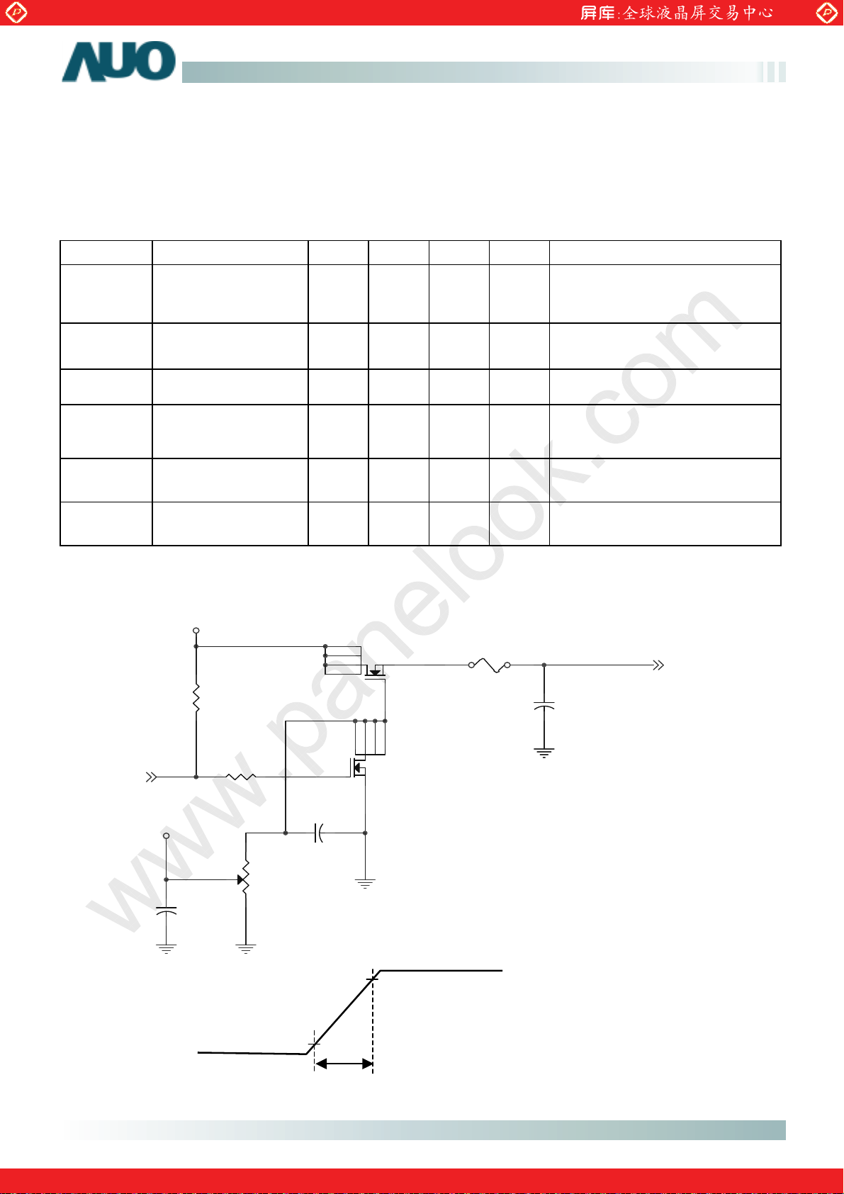
Note: Measurement conditions:
(High to Low)
Control Signal
SW
+12.0V
+5.0V
C2
1uF/25V
R1
47K
Q3
AO6402
D6
D5
D2 S
D1
G
D2SD1D5
D6
R2
1K
VR1
47K
G
C3
0.01uF/25V
Q3
AO6402
F1
VCC
(LCD Module Input)
C1
1uF/16V
5.0V
0V
470 us
Vin rising time
Ve
r0.4 14/28
One step solution for LCD / PDP / OLED panel application: Datasheet, inventory and accessory!
www.panelook.com
Page 14
Global LCD Panel Exchange Center
www.panelook.com
Product Specification
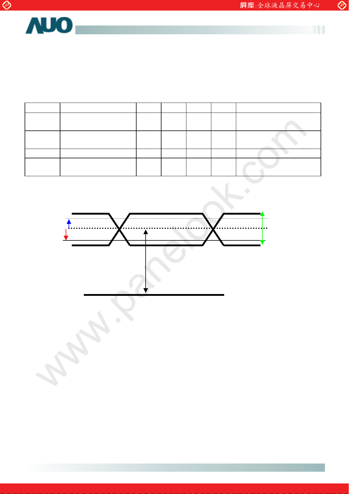
5.1.2 Signal Electrical Characteristics
Input signals shall be low or Hi-Z state when Vin is off
It is recommended to refer the specifications of SN75LVDS82DGG (Texas Instruments) in detail.
Each signal characteristics are as follows;
M190EN03 V.3
mbol Parameter Min Ty
Sy
VTH
VTL
VID
│
VICM
Note: LVDS Signal Waveform
VTH
VTL
Differential Input High
Threshold
Differential Input Low
Threshold
Input Differential Voltage
│
Differential Input Common
Mode Voltage
VICM
- -
-100 -
100 400 600 [mV] Note
+1.
p Max Units Condition
+100
-
+1.2 +1.35 [V]
0
[mV]
[mV]
VICM = 1.2V
Note
VICM = 1.2V
Note
VTH/VTL = 100mV
Note
ѨVIDѨ
VSS
Ve
r0.4 15/28
One step solution for LCD / PDP / OLED panel application: Datasheet, inventory and accessory!
www.panelook.com
Page 15
Global LCD Panel Exchange Center
5.2 Backlight Unit
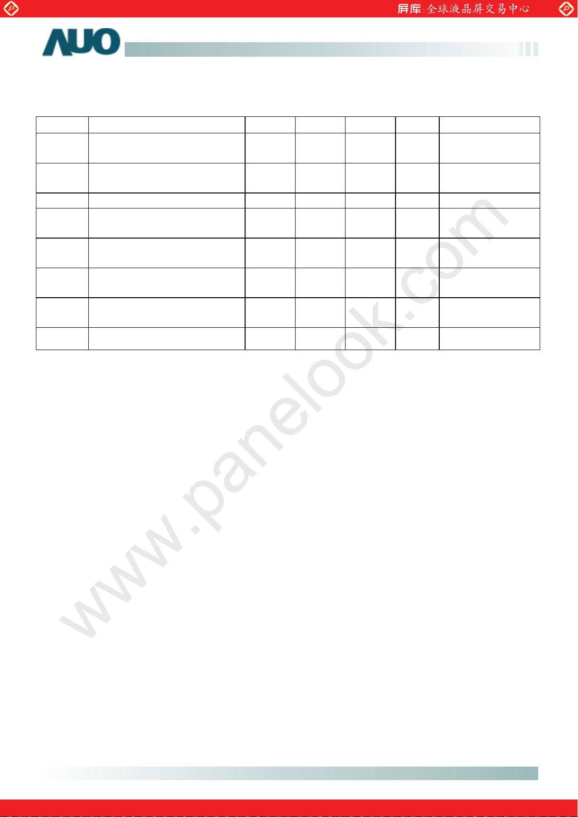
Parameter guideline for CCFL Inverter
www.panelook.com
M190EN03 V.3
Product Specification
mbol Parameter Min. Ty
Sy
ISCFL CCFL
IRCFL
standard current 6.5 7.0 7.5
CCFL
operation range
2.5 7.0 7.5
p. Max. Unit Condition
[mA]
rms
[mA]
rms
(Ta=25
(Ta=25
o
C) Note 1
o
C)
FCFL CCFL Frequency 40 50 60 [KHz] (Ta=25oC) Note 2
ViC
FL
o
C)
(0
Vi
F
C
o
C)
(25
VCFL
PCFL
CFL CCFL life Time 40,000 50,000 - [Hour] (Ta=25
LT
Note 1: CCFL st
CCFL Ignition V
oltage
(End of the lamp wire connector)
CCFL Ignition V
oltage
(End of the lamp wire connector)
CCFL Operation V
oltage
(For reference)
CCFL Power consumption (for
reference)
andard current is measured at 252к..
1810 - -
1540 - -
-
750
@7mA
- 21
800
23.1 [Watt] (Ta=25
[Volt]
rms
[Volt]
rms
[Volt]
rms
(Ta=0
(Ta=25
(Ta=25
o
C) No
o
C) Note 3
o
C) Note 4
o
C) Note 5
o
C) Note 6
te 3
Note 2: CCFL Frequency should be carefully determined to avoid interference between inverter and TFT LCD
Note 3: ViCFL means Ignition Voltage for both ends of the lamp, and CCFL inverter should be able to give out a power that
has a generating capacity of over 1810 voltage. Lamp units need 1810 voltage minimum for ignition
Note 4: CCFL operation voltage is measured at 252к.
Note 5: The variance of CCFL power consumption is ᇹ10%. Calculator value for reference
(ICFL×VCFL×4=PCFL).
Note 6: Definition of life: brightness becomes 50% or less than the minimum luminance value of CCFL..The
typical life time of CCFL is on the condition at 7.0mA lamp current.
Ve
r0.4 16/28
One step solution for LCD / PDP / OLED panel application: Datasheet, inventory and accessory!
www.panelook.com
Page 16
Global LCD Panel Exchange Center
www.panelook.com
Product Specification
6.0 Signal Characteristic
6.1 Pixel Format Image
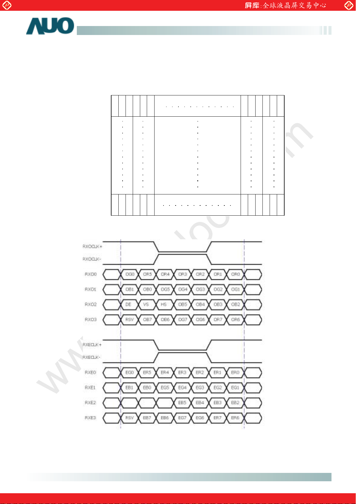
Following figure shows the relationship of the input signals and LCD pixel format.
1 2 1279 1280
M190EN03 V.3
1s
t Line
1024 Line
6.2 The input data format
R G B R G B
R G B R G B
R G B R G B
R G B R G B
Note 1: R/G/B data 7:MSB, R/G/B data 0:LSB
O = “First Pixel Data”
E = “Second Pixel Data”
Ve
r0.4 17/28
One step solution for LCD / PDP / OLED panel application: Datasheet, inventory and accessory!
www.panelook.com
Page 17
Global LCD Panel Exchange Center
g
)
put(
)
g
)
put(
)
)
put(
)
)
put(
)
g
)
put(
)
g
)
)
put(
)
)
)
put(
)
)
put(
)
g
put(
)
)
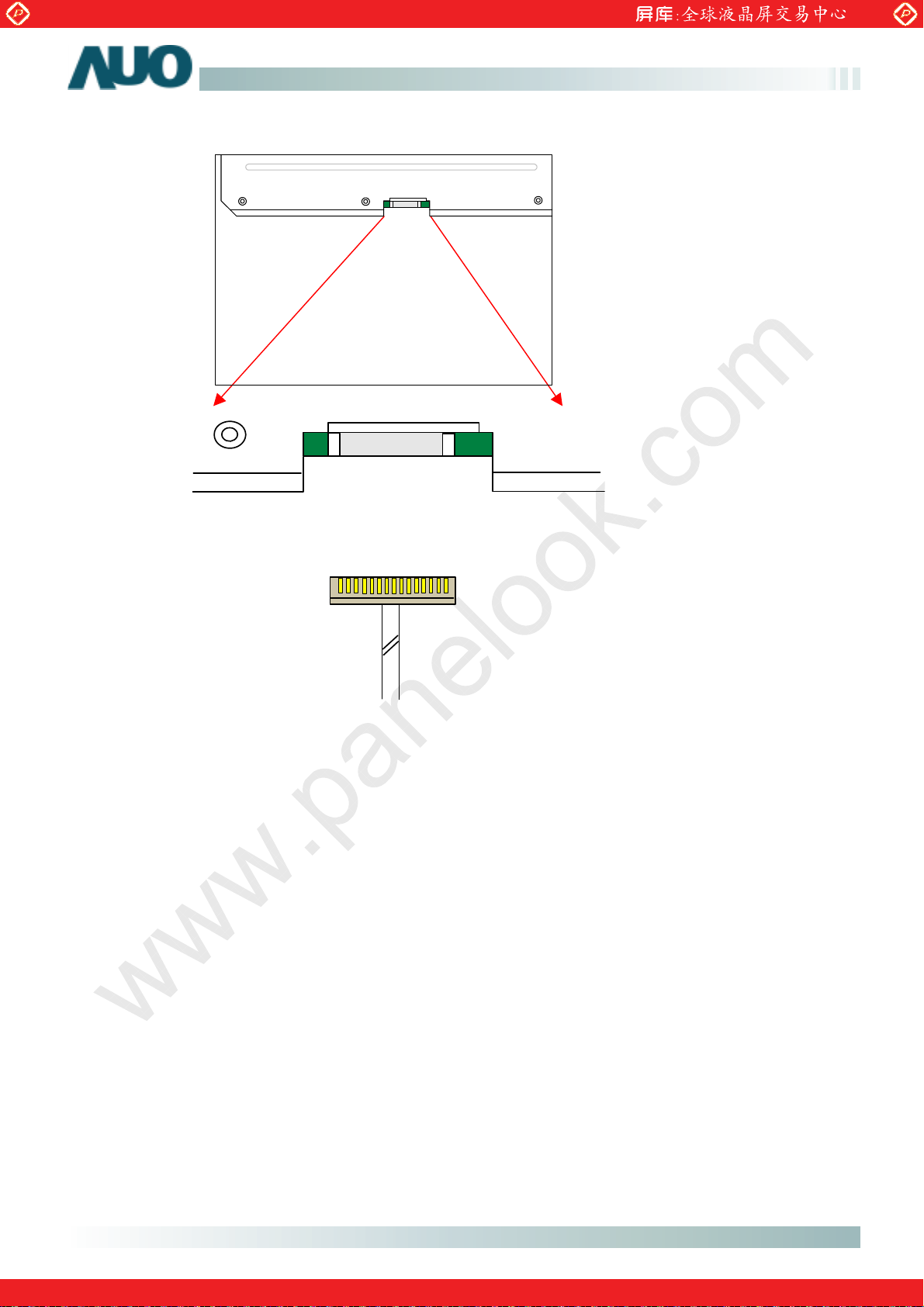
6.3 Signal Description
www.panelook.com
M190EN03 V.3
Product Specification
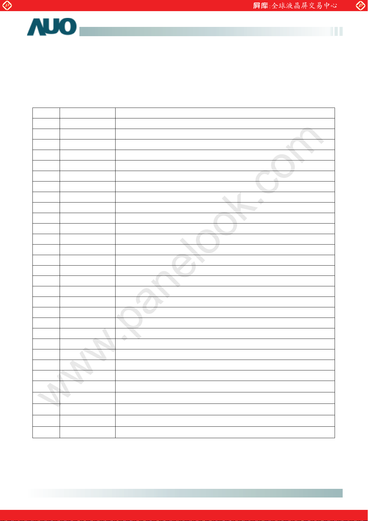
The module
differential signal technology for LCD interface and high speed data transfer device. Transmitter shall be
SN75LVDS83(negative edge sampling) or compatible. The first LVDS port(RxOxxx) transmits odd pixels
while the second LVDS port(RxExxx) transmits even pixels.
PIN # SIGNAL NAME DESCRIPTION
1 RxOIN0-
2 RxOIN0+
3 RxOIN1-
4
5 RxOIN2- Negative LVDS differential data input(Odd data, H-Sync,V-Sync,DSPTMG
6 RxOIN2+
7 VSS Power
8 RxOCLKIN- Negative LVDS differential clock input(Odd clock
9
10 RxOIN3-
11 RxOIN3+
12 RxEIN0-
13 RxEIN0+ Positive LVDS differential data input(Even data
14 VSS Power
15 RxEIN1-
16 RxEIN1+ Negative LVDS differential data input(Even data
17 VSS Power
18 RxEIN2- Negative LVDS differential data input(Even data
19 RxEIN2+
20 RxECLKIN- Negative LVDS differential clock input(Even clock
21 RxECLKIN+
22 Rx
23 RxEIN3+ Positive LVDS differential data input(Even data
24 VSS Power
25 NC -
26 NC -
using one LVDS receiver SN75LVDS82(Texas Instruments) or compatible. LVDS is a
ative LVDS differential data input(Odd data
Ne
RxOIN1+
RxOCLKIN+
EIN3-
Positive LVDS differential data in
ative LVDS differential data input(Odd data
Ne
Positive LVDS differential data in
Positive LVDS differential data in
Ground
Positive LVDS differential clock in
Ne
ative LVDS differential data input(Odd data
Positive LVDS differential data in
Ne
ative LVDS differential data input(Even clock
Ground
Positive LVDS differential data in
Ground
Positive LVDS differential data in
Positive LVDS differential clock in
ative LVDS
Ne
Ground
differential data in
Odd data
Odd data
Odd data, H-Sync,V-Sync,DSPTMG
Odd clock
Odd data
Even data
Even data
Even clock
Even data
27 NC -
28
29 VCC +5.0V Power Supply
30 VCC +5.0V Power Supply
One step solution for LCD / PDP / OLED panel application: Datasheet, inventory and accessory!
VCC +5.0V Power Supply
Ve
r0.4 18/28
www.panelook.com
Page 18
Global LCD Panel Exchange Center
RxO
IN
0
VCC
Note1: Start from left side
www.panelook.com
M190EN03 V.3
Product Specification
Connector
-
Note2: Input signals of odd and even clo
30
ck shall be the same timing.
Ve
One step solution for LCD / PDP / OLED panel application: Datasheet, inventory and accessory!
r0.4 19/28
www.panelook.com
Page 19
Global LCD Panel Exchange Center
6
4
G
www.panelook.com
M190EN03 V.3
Product Specification
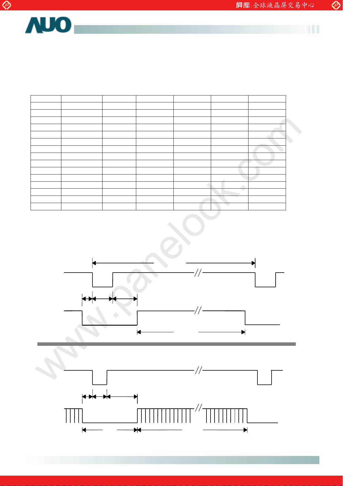
6.4.1 Timing Characteristics
Basically, interface timings described here is not actual input timing of LCD module but output timing of
SN75LVDS82DGG (Texas Instruments) or equivalent. Note: Typical value refer to VESA STANDARD
Signal Item Symbol MIN TYP MAX Unit
DTCLK Freq.
DTCLK Cycle Tck
+V-Sync Frame Rate
+V-Sync Cycle Tv
+V-Sync Cycle Tv
+V-Sync Active level
+V-Sync V-back porch
+V-Sync V-front porch
+DSPTMG V-Line m
+H-Sync Scan rate
+H-Sync Cycle Th
+H-Sync Active level
+H-Sync Back porch Thb (*1) 4 124 Tck
+H-Sync Front porch
+DSPTMG Display Pixels n - 640 - Tck
Fdck 50 67.5 70 MHz
14.2 14.8 20 ns
1/Tv 56.25 75 77 Hz
13 13.33 17.78 ms
1035 1066 2047 lines
Tva 3 3 lines
Tvb 7 38 63 lines
Tvf 1 1 lines
- 1024 - lines
1/Th - 80.06 - KHz
800 844 1023 Tck
Tha (*1) 4 56 Tck
Thf 4 24 Tck
6.4.2 Timing diagram
H-Sync
dot
DSPTMG
V- Sync
1H
844do
12
dot24
dot
5
t
640dot
38H
3H
DSPTM
Ve
r0.4 20/28
One step solution for LCD / PDP / OLED panel application: Datasheet, inventory and accessory!
www.panelook.com
Page 20
Global LCD Panel Exchange Center
www.panelook.com
M190EN03 V.3
Product Specification
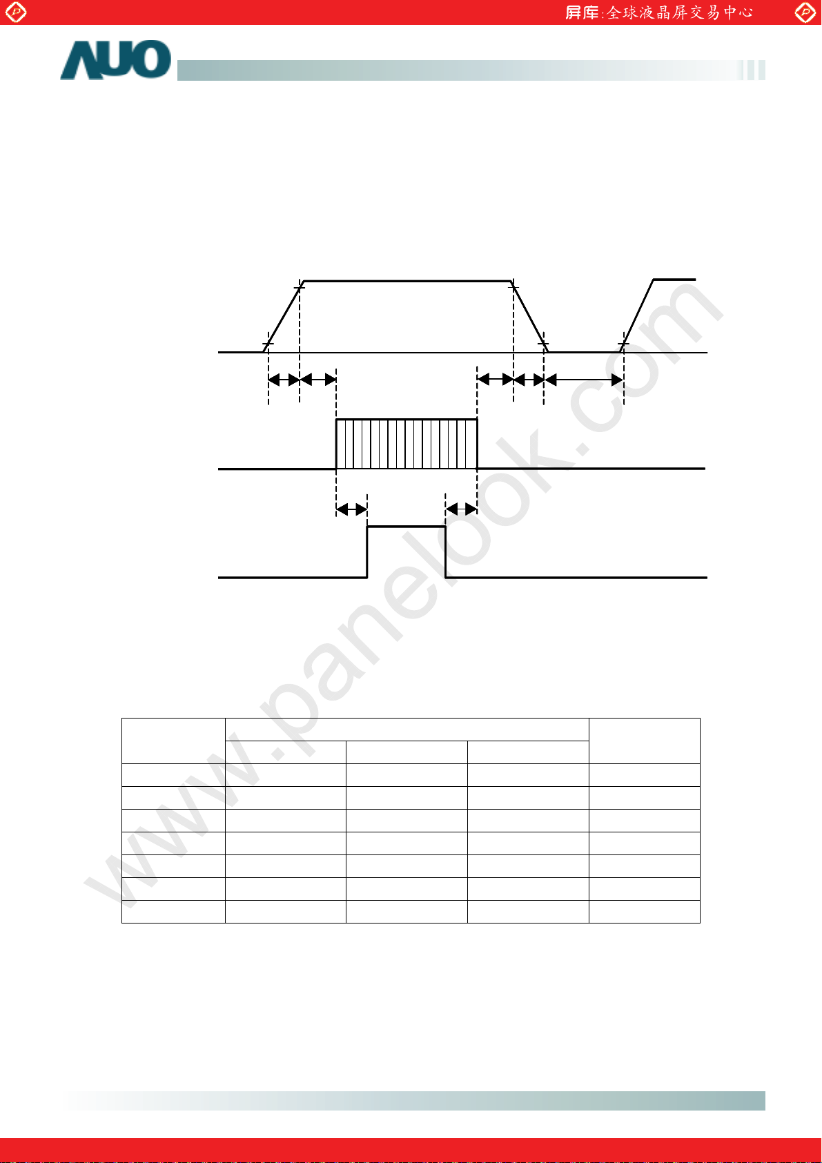
6.5 Powe
Vin power and lamp on/off sequence is as follows. Interface signals are also shown in the chart. Signals
from any system shall be Hi-Z state or low level when Vin is off.
r ON/OFF Sequence
90% 90%
90% 90%
90% 90%
10%
10%
Vin 10%
Vin 10%
Vin 10%
0V
0V
0V
Signal
Signal
Signal
0V
0V
0V
10%
T2 T5 T6 T7
T2 T5 T6 T7
T2 T5 T6 T7
T1
T1
T1
T4
T4
T3
T3
T3
T4
10%
10%
10%
Lam
Lam
Lam
p
p
p
0V
0V
0V
Symbol
Min Ty
T1 0.5 - 10 [ms]
T2 0.5 40
T3 200 -
T4 200 - - [ms]
T5 0.5 16
T6 0.5
T7 1000 -
Values
p Max
50 [ms]
- [ms]
50 [ms]
-
10 [ms]
- [ms]
Unit
Ve
r0.4 21/28
One step solution for LCD / PDP / OLED panel application: Datasheet, inventory and accessory!
www.panelook.com
Page 21
Global LCD Panel Exchange Center
www.panelook.com
Product Specification
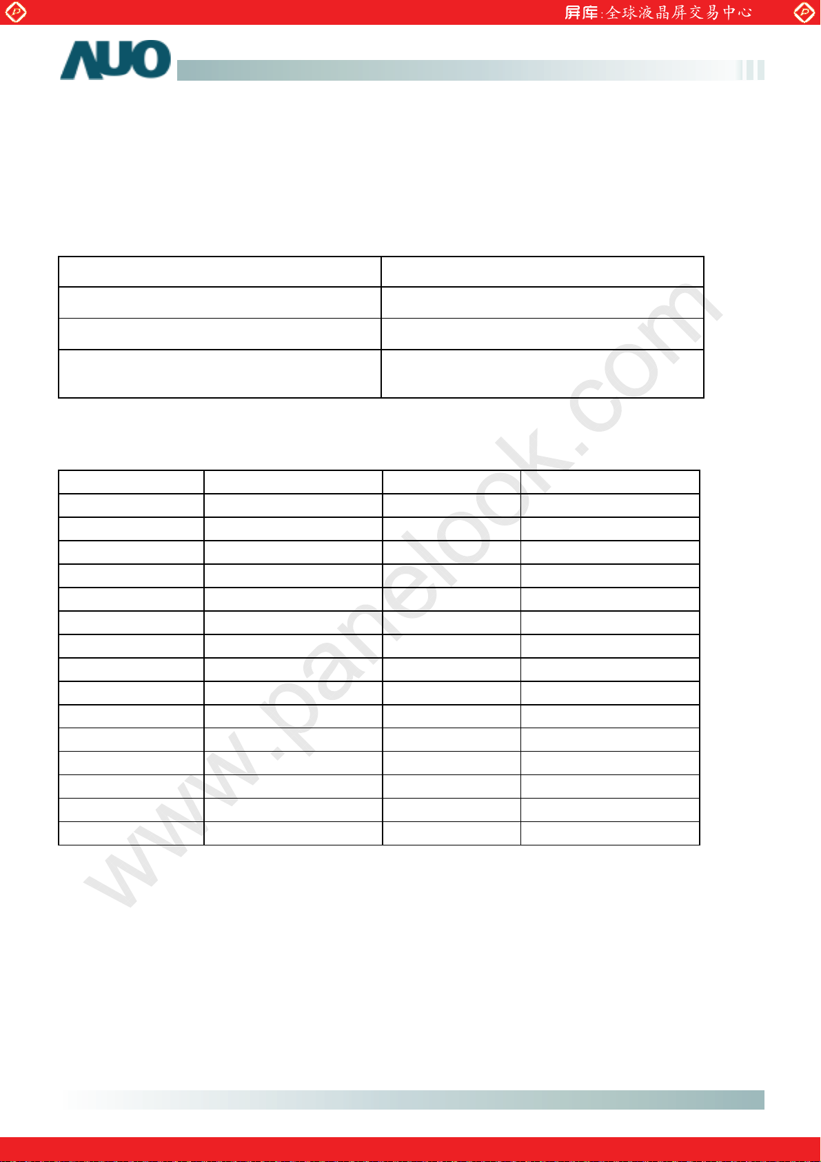
7.0 Connector & Pin Assignment
Physical interface is described as for the connector on module.
These connectors are capable of accommodating the following signals and will be following components.
7.1 TFT LCD Module
M190EN03 V.3
Connector Name / Designation Interface Connector
Manufacturer HIROSE/JAE or c
Typ
e Part Number MDF 76KBW-30S-1H(58)/ FI-XB30SL-HF10
Mating Housing Part Number
Pin# Signal Name Pin# Signal Name
1 RxOIN0-
3 RxOIN1-
5 RxOIN2-
7 VSS 8 RxOCLKIN-
9 RxOCLKIN+ 10
11 RxOIN3+
13 RxEIN0+
15 RxEIN1-
17 VSS 18 RxEIN2-
19 RxEIN2+ 20
21 RxECLKIN+ 22
23 RxEIN3+
25 NC
27 NC 28 VCC
29 VCC 30
MDF 70G-30P-1SD/
FI-X30S-H ( Unlocked T
2 RxOIN0+
4 RxOIN1+
6 RxOIN2+
12 RxEIN0-
14 VSS
16 RxEIN1+
24 VSS
26
/ Interface card
ompatible
FI-X30HL-T ( Locked
ype )
RxOIN3-
RxECLKIN-
RxEIN3-
NC
VCC
Type ),
Ve
r0.4 22/28
One step solution for LCD / PDP / OLED panel application: Datasheet, inventory and accessory!
www.panelook.com
Page 22
Global LCD Panel Exchange Center
www.panelook.com
Product Specification
7.2 Backlight Unit
Connector Name / Designation Lamp Connector / Backlight lamp
Manufacturer JST
Typ e P a r t N u m b e r BHSR-02VS-1
M190EN03 V.3
Mating Ty
pe Part Number SM02B-BHSS-1-TB
7.3 Signal for Lamp connector
Connector No. Pin No. Input Color Function
CN1
Upper
CN2
CN3
Lower
CN4
1 Hot1 Pink
2 Cold1 White
1 Hot2 Pink
2 Cold2 White
1 Hot1 Pink
2 Cold1
1 Hot2 Pink
2 Cold2
8.0 Vibration, Shock, and Drop
8.1 Vibration & Shock
Vibration Test Spec:
z
z
Frequency: 10 - 200Hz
Sweep:
30 Minutes each Axis (X, Y, Z)
White
White
High Voltage
Low Voltage
High Voltage
Low Voltage
High Voltage
Low Voltage
High Voltage
Low Voltage
z
z
Shock Test Spec:
z Direction: X , Y, Z
Acceleration: 1.5G(10~200Hz P- P)
Test method:
Acceleration (G) 1.5
Frequency (Hz) 10~200~10
Active tim
Acceleration (G) –a 50
Active
Wave form
Times 1
e (min) 30
time -b 20 ms
Half-sin
Ve
r0.4 23/28
One step solution for LCD / PDP / OLED panel application: Datasheet, inventory and accessory!
www.panelook.com
Page 23
Global LCD Panel Exchange Center
www.panelook.com
Product Specification
8.2 Drop test
Package test: The drop height is 60cm.
9.0 Environment
The display module will meet the provision of this specification during operating condition or after storage
or shipment condition specified below. Operation at 10% beyond the specified range will not
physical damage to the unit.
9.1 Temperature and Humidity
9.1.1 Operating Conditions
The display module operates error free, when operated under the following conditions;
Temperature
Relative Humidity 8
Wet Bulb Temperature 39.0
0
0
C to 50 0C
% to 95%
0
C
M190EN03 V.3
cause
9.1.2 Shipping Conditions
The display module operates error free, after the following conditions;
Temperature
Relative Humidity 8
Wet Bulb Temperature 39.0
9.2 Atmospheric Pressure
The display assembly is capable of being operated without affecting its operations over the
pressure range as following specified;
Maximum Pressure 1040hPa 0m = sea level
Minimum Pressure 674hPa 3048m = 10.000 feet
Note : Non-operation attitude limit of this display module = 30,000 feet. = 9145 m.
9.3 Thermal Shock
The display module will not sustain damage after being subjected to 100 cycles of rapid
temperature change. A cycle of rapid temperature change consists of varying the temperature
from -20
0
C to 600C, and back again.
-20
0
C to 60 0C
% to 95%
0
C
Pressure Note
0
C for 30min
Thermal shock cycle
60
-20
0
C for 30min
Power is not applied during the test. After temperature cycling, the unit is placed in normal room
ambient for at least 4 hours before powering on.
Ve
r0.4 24/28
One step solution for LCD / PDP / OLED panel application: Datasheet, inventory and accessory!
www.panelook.com
Page 24
Global LCD Panel Exchange Center
www.panelook.com
Product Specification
10.0 Reliability
This display module and the packaging of that will comply following standards.
10.1 Failure Criteria
The display assembly will be considered as failing unit when it no longer meets any of the
requirements stated in this specification. Only as for maximum white luminance, following criteria
is applicable.
z Maximum w
hite Luminance shall be 125cd/m
10.2 Failure Rate
The average failure rate of the display module (from first power-on cycle till 1,000 hours later) will not
exceed 1.0%. The average failure rate of the display module from 1,000 hours until 16,000 hours will not
exceed 0.7% per 1000 hours.
2
or more.
M190EN03 V.3
10.2.1 Usage
The assumed usage for the above criteria is:
z 220 power-on hours per month
z 500 power on/off cycles per month
z Maximum brightness setting
z Operation to be within office environment (25
0
C ty
pical)
10.2.1 Component De-rating
All the components used in this device will be checked the load condition to meet the failure rate
criteria.
10.3 On/OFF Cycle
The display module will be capable of being operated over the following ON/OFF Cycles.
ON/OFF Value
+Vin and CCFL power 30,000 10 seconds on / 10 seconds off
Cy
cles
Ve
r0.4 25/28
One step solution for LCD / PDP / OLED panel application: Datasheet, inventory and accessory!
www.panelook.com
Page 25
Global LCD Panel Exchange Center
11.0 Safety
11.1 Sharp Edge Requirements
There will be no sharp edges or comers on the display assembly that could cause injury.
11.2 Materials
11.2.1 Toxicity
There will
materials are used, they will be reviewed and approved by the responsible ADT
Toxicologist.
11.2.2 Flammability
All components including electrical components that do not meet the flammability
UL94-V1 in the module will complete the flammability rating exception approval process.
be no carcinogenic materials used anywhere in the display module. If toxic
www.panelook.com
M190EN03 V.3
Product Specification
grade
The printed circuit board will be made from material rated 94-V1 or better.
flammability rating will be printed on the printed circuit board.
11.3 Capacitors
If any
polarized capacitors are used in the display assembly, provisions will be made to keep
them from being inserted backwards.
12.0 Other requirement
12.1 National Test Lab Requirement
The display module will satisfy all requirements for compliance to
UL 1950, First Edition
CSA C22.2 No.950-M89 Canada, Information Technology Equipment
EEC 950 International, Information Technology Equipment
EN 60 950 International, Information Processing Equipment
(European Norm for IEC950)
U.S.A. Information Technology Equipment
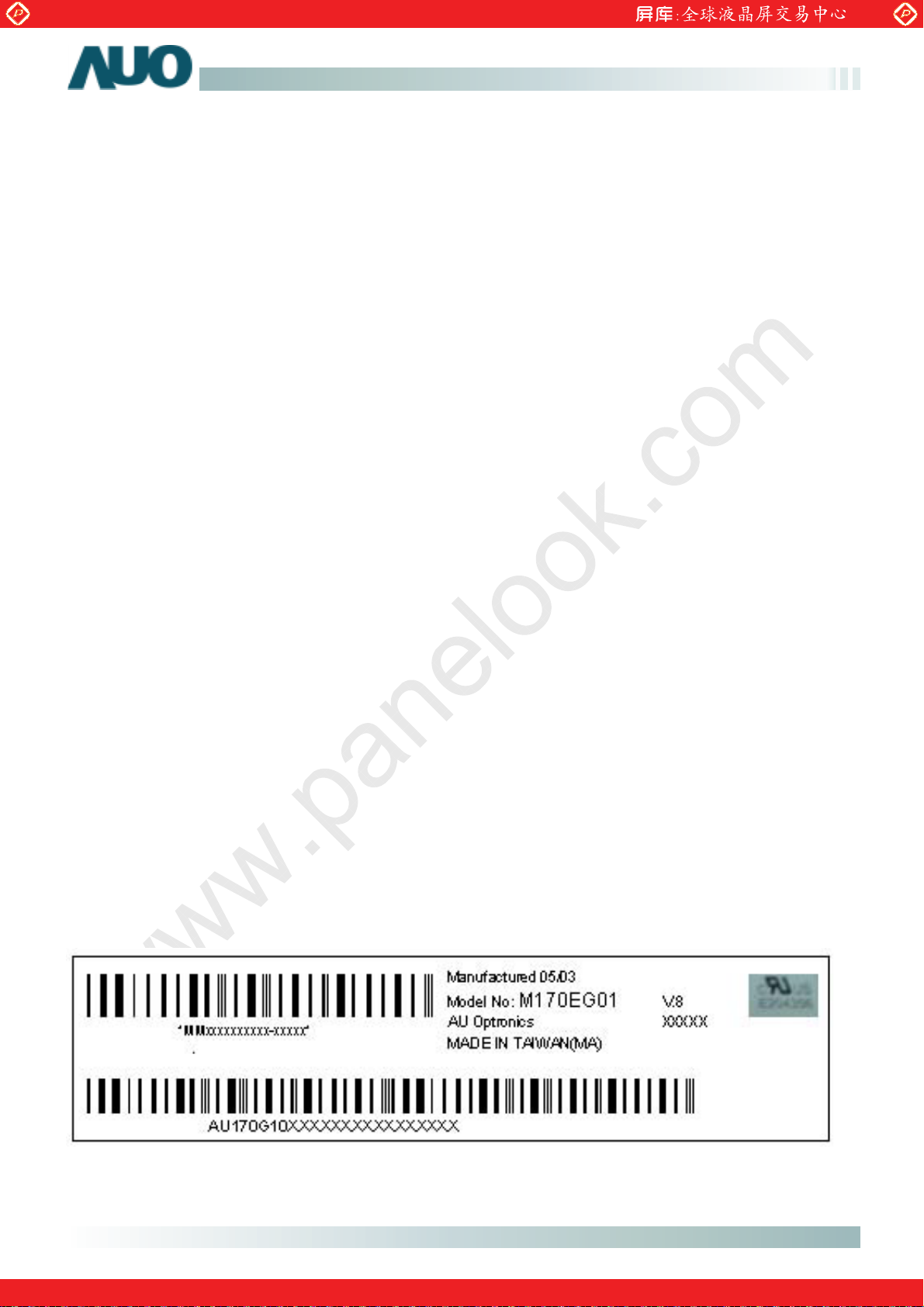
12.2 Label
The label is on the panel as shown below:
The actual UL
(For reference)
Ve
r0.4 26/28
One step solution for LCD / PDP / OLED panel application: Datasheet, inventory and accessory!
www.panelook.com
Page 26
Global LCD Panel Exchange Center
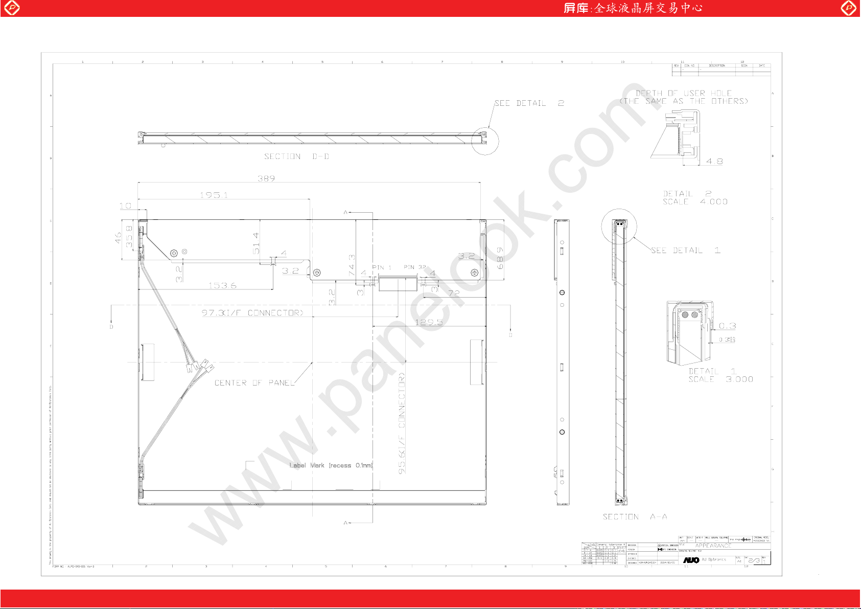
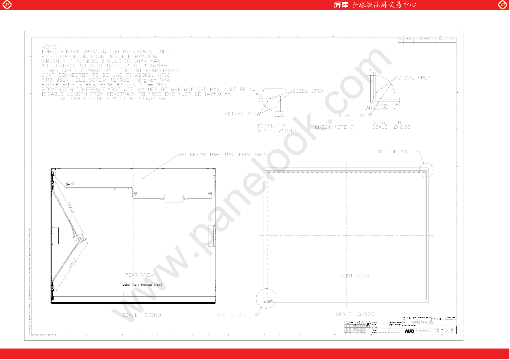
13.0 Mechanical Characteristics
www.panelook.com
Ver0
.4 27/29
One step solution for LCD / PDP / OLED panel application: Datasheet, inventory and accessory!
www.panelook.com
Page 27
Global LCD Panel Exchange Center
www.panelook.com
Ver0
.4 28/29
One step solution for LCD / PDP / OLED panel application: Datasheet, inventory and accessory!
www.panelook.com
Page 28
Global LCD Panel Exchange Center
www.panelook.com
Ver0
.4 29/29
One step solution for LCD / PDP / OLED panel application: Datasheet, inventory and accessory!
www.panelook.com
 Loading...