

Page 1

Global LCD Panel Exchange Center
AU OPTRONICS CORPORATION
www.panelook.com
Spec. No.: DDPM-ES05-0.1
Version: 2
Total pages: 28
Date: 2003-May-09
Product Specifications
17.0” SXGA Color TFT-LCD Module
Model Name: M170ES05
V.2
Approved by Prepared by
DDBU Marketing Division / AU Optronics Croporation
Customer Checked & Approved by
(C) Copyright AU Optronics, Inc.
January, 2002 All Rights Reserved. M170ES05 v.2 Ver0.1
No Reproduction and Redistribution Allowed.
One step solution for LCD / PDP / OLED panel application: Datasheet, inventory and accessory!
1/28
www.panelook.com
Page 2

Global LCD Panel Exchange Center
www.panelook.com
Product Specifications
17.0” SXGA Color TFT-LCD Module
Model Name: M170ES05
V.2
() Preliminary Specifications
( ) Final Specifications
Note: This Specification is subject to change without notice.
(C) Copyright AU Optronics, Inc.
January, 2002 All Rights Reserved. M170ES05 v.2 Ver0.1
No Reproduction and Redistribution Allowed.
One step solution for LCD / PDP / OLED panel application: Datasheet, inventory and accessory!
2/28
www.panelook.com
Page 3

Global LCD Panel Exchange Center
i Contents
ii Record of Revision
1.0 Handling Precautions
2.0 General Description
2.1 Display Characteristics
2.2 Functional Block Diagram
2.3 Optical Characteristics
2.4 Pixel format image
3.0 Electrical characteristics
3.1 Absolute Maximum Ratings
3.2 Connectors
3.3 Signal Pin & Description
3.4 RSDS Signal Electrical Characteristic
3.5 Timing Requirement
3.6 Electrical Rating
3.7 Power ON/OFF Sequence
4.0 Backlight Characteristics
4.1 Signal for Lamp connector
4.2 Parameter guide line for CCFL Inverter
5.0 Vibration, shock and drop
5.1 Vibration and shock
5.2 Drop test
6.0 Environment
6.1 Temperature and humidity
6.1.1 Operating conditions
6.1.2 Shipping conditions
6.2 Atmospheric pressure
6.3 Thermal shock
7.0 Reliability
7.1 Failure criteria
7.2 Failure rate
7.2.1 Usage
7.2.2 Components de-rating
7.3 CCFL life
7.4 ON/OFF cycle
8.0 Safety
8.1 Sharp edge requirement
8.2 Material
8.2.1 Toxicity
8.2.2 Flammability
8.3 Capacitors
8.4 Hazardous voltage
9.0 Other requirements
9.1 Smoke free design
9.2 National test lab requirement
10.0 Mechanical Characteristics
www.panelook.com
(C) Copyright AU Optronics, Inc.
January, 2002 All Rights Reserved. M170ES05 v.2 Ver0.1
No Reproduction and Redistribution Allowed.
One step solution for LCD / PDP / OLED panel application: Datasheet, inventory and accessory!
3/28
www.panelook.com
Page 4
Global LCD Panel Exchange Center
www.panelook.com
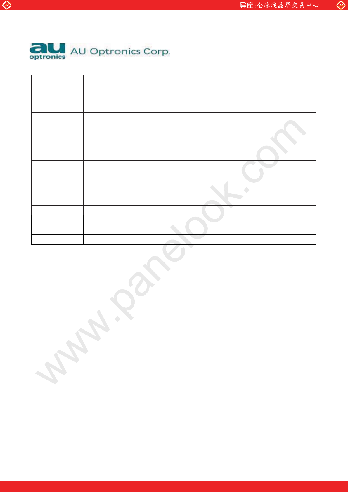
ii Record of Revision
Version and Date Page Old description New Description Remark
0.1 2003/5/09 All First Edition for Customer All
(C) Copyright AU Optronics, Inc.
January, 2002 All Rights Reserved. M170ES05 v.2 Ver0.1
No Reproduction and Redistribution Allowed.
One step solution for LCD / PDP / OLED panel application: Datasheet, inventory and accessory!
4/28
www.panelook.com
Page 5

Global LCD Panel Exchange Center
www.panelook.com
1.0 Handling Precautions
1) Since front polarizer is easily damaged, pay attention not to scratch it.
2) Be sure to turn off power supply when inserting or disconnecting from input connector.
3) Wipe off water drop immediately. Long contact with water may cause discoloration or spots.
4) When the panel surface is soiled, wipe it with absorbent cotton or other soft cloth.
5) Since the panel is made of glass, it may break or crack if dropped or bumped on hard surface.
6) Since CMOS LSI is used in this module, take care of static electricity and insure human earth when
handling.
7) Do not open nor modify the Module Assembly.
8) Do not press the reflector sheet at the back of the module to any directions.
9) At the insertion or removal of the Signal Interface Connector, be sure not to rotate nor tilt the Interface
Connector of the TFT-LCD module.
10) After installation of the TFT-LCD module into an enclosure (LCD monitor housing, for example), do not
twist nor bend the TFT -LCD module even momentary. At designing the enclosure, it should be taken into
consideration that no bending/twisting forces are applied to the TFT -LCD module from outside.
Otherwise the TFT -LCD module may be damaged.
(C) Copyright AU Optronics, Inc.
January, 2002 All Rights Reserved. M170ES05 v.2 Ver0.1
No Reproduction and Redistribution Allowed.
One step solution for LCD / PDP / OLED panel application: Datasheet, inventory and accessory!
5/28
www.panelook.com
Page 6
Global LCD Panel Exchange Center
C
pp
N
(yp)
T
SC
()
4
T
y
p
0
50
www.panelook.com
General Description
This specification applies to the 17.0 inch Color TFT-LCD Module M170ES05.
The display supports the SXGA (1280(H) x 1024(V)) screen format and 262K colors (RGB 6-bits data).
All input signals are 2 Channel RSDS interface compatible.
This module does not contain an inverter card for backlight.
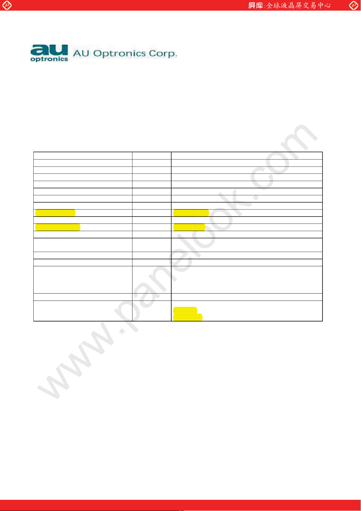
2.1 Display Characteristics
The following items are characteristics summary on the table under 25 condition:
ITEMS Unit SPECIFICATIONS
Screen Diagonal [mm] 432(17.0")
Active Area [mm] 337.920 (H) x 270.336(V)
Pixels H x V 1280(x3) x 1024
Pixel Pitch [mm] 0.264 (per one triad) x 0.264
Pixel Arrangement R.G.B. Vertical Stripe
Display Mode Normally White
White Luminance [cd/m2] 300 (center) @ 7mA
Contrast Ratio 450 : 1 (Typ)
Contrast Ratio
Optical Response Time [msec] 16 (Typ.)
Color Saturation 72% NTSC
olor Saturation
Nominal Input Voltage VDD [Volt] +5.0 V
Power Consumption
(VDD line + CCFL line)
Weight [Grams] 2000 (Typ)
Physical Size [mm] 358.5(W) x 296.5(H) x 19.0(D)
Electrical Interface Front R/G/B data (6bits) and clock pairs
Support Color 262k colors (RGB 6-bit data )
Temperature Range
Operating
Storage (Shipping)
[Watt] 25W (w/o Inverter, All black pattern) (typ.)
o
C]
[
o
C]
[
50 : 1 (
72%
Back R/G/B data (6bits) and clock pairs
7 timing control signal input
4 DC power input
0 to +50
to +
-20 to +60
-20 to +60
)
(C) Copyright AU Optronics, Inc.
January, 2002 All Rights Reserved. M170ES05 v.2 Ver0.1
No Reproduction and Redistribution Allowed.
One step solution for LCD / PDP / OLED panel application: Datasheet, inventory and accessory!
6/28
www.panelook.com
Page 7
Global LCD Panel Exchange Center
www.panelook.com
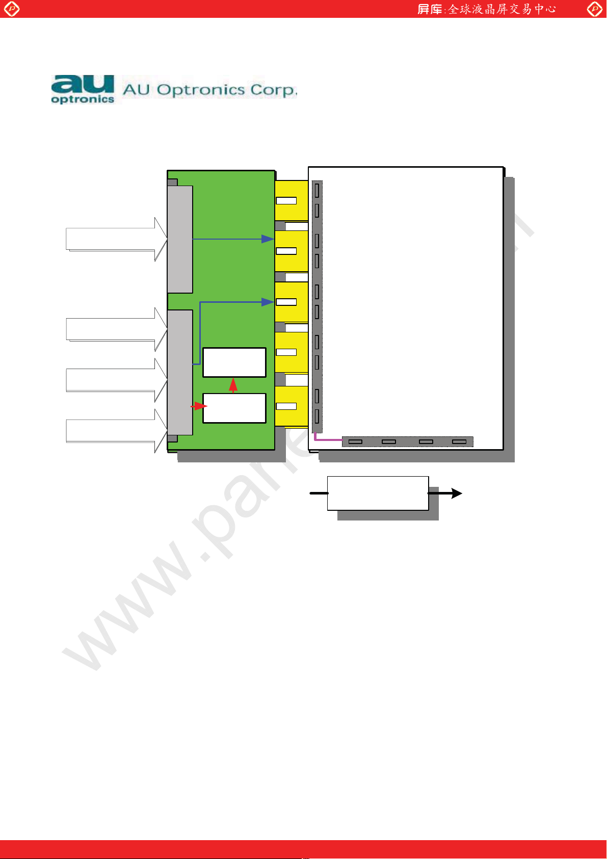
2.2 Functional Block Diagram
The following diagram shows the functional block of the 17.0 inches Color TFT-LCD Module:
D
D
3
3
8
8
4
4
0
0
S
S
o
o
u
u
r
r
c
c
e
e
D
D
r
r
i
i
v
v
e
e
r
r
I
I
C
C
D
D
1
1
G1 G1024
TFT-LCD
TFT-LCD
1280*(3)*102
1280*(3)*1024
4
Pixels
Pixels
Gate Driver IC
G1 G1024
Gate Driver IC
Back RSDS Signals
LVDS Signals
Front RSDS Signals
LVDS Signals
Countrol Signals
LVDS Signals
+5V DC Input
LVDS Signals
H
I
R
A
O
F
S
7
E
P
3
0
-
F
T
1
H
W
-
A
-
1
O
2
2
G
3
1
0
T
p
i
n
s
H
I
R
A
O
F
S
7
P
E
5
-
0
T
F
1
W
H
-
A
-
O
1
2
2
G
5
1
0
T
p
i
n
s
Back Differential
X6~X10
X6~X10
Back Differential
Pairs Signals
Pairs Signals
X1~X5
X1~X5
Front Differential
Front Differential
Pairs Signals
Pairs Signals
Gamma
Gamma
Correction
Correction
DC-DC
DC-DC
Converter
Converter
FPC
FPC
FPC
FPC
FPC
FPC
FPC
FPC
FPC
FPC
X
PCB
DC
Inverter 4 CCFL
power
P-TWO AF7301-A2G1T JST BHR-04VS-1
&
P-TWO AF7501-A2G1T Mating Type: SM04(4.0)B-BHS-1-TB
(C) Copyright AU Optronics, Inc.
January, 2002 All Rights Reserved. M170ES05 v.2 Ver0.1
No Reproduction and Redistribution Allowed.
7/28
One step solution for LCD / PDP / OLED panel application: Datasheet, inventory and accessory!
www.panelook.com
Page 8

Global LCD Panel Exchange Center
Definition o
Response ti
e:
www.panelook.com
2.3 Optical Characteristics
The optical characteristics are measured under stable conditions at 25 (Room Temperature):
Item Unit Conditions Min. Typ. Max.
Horizontal (Right)
CR = 10 (Left)
Vertical (Up)
Viewing Angle (Note 4) [degree]
Contrast ratio
Response Time (Note 1) [m sec]
Color / Chromaticity
Coordinates (CIE)
Color Coordinates (CIE) White
White Luminance @ CCFL 7.0mA
(center)
Luminance Uniformity (Note 2) [%] 75 80 Cross-talk (in 75Hz) (Note 5) [%] 1.5
[cd/m2] 230 300 -
CR = 10 (Down)
Horizontal (Right)
CR = 5 (Left)
Vertical (Up)
CR = 5 (Down)
Normal Direction 250 450 -
Raising Time - 4 5
Falling Time - 12 20
Raising + Falling - 16 25
Red x 0.61 0.64 0.67
Red y 0.31 0.34 0.37
Green x 0.26 0.29 0.32
Green y 0.58 0.61 0.64
Blue x 0.11 0.14 0.17
Blue y 0.04 0.07 0.10
White x 0.28 0.31 0.34
White y 0.30 0.33 0.36
60
60
60
60
70
70
70
70
70
70
70
70
80
80
80
80
-
-
-
-
-
-
Note 1: Definition of Response time:
The output signals of photo detector are measured when the input signals are changed from “ Black” to “ White”
(falling time), and from “White” to “ Black” (rising time), respectively. The response time is interval between the 10%
and 90% of amplitudes.
TrR
%
100
90
Optical
Response
10
(C) Copyright AU Optronics, Inc.
January, 2002 All Rights Reserved. M170ES05 v.2 Ver0.1
No Reproduction and Redistribution Allowed.
white
0
black
TrD
white
8/28
One step solution for LCD / PDP / OLED panel application: Datasheet, inventory and accessory!
www.panelook.com
Page 9
Global LCD Panel Exchange Center
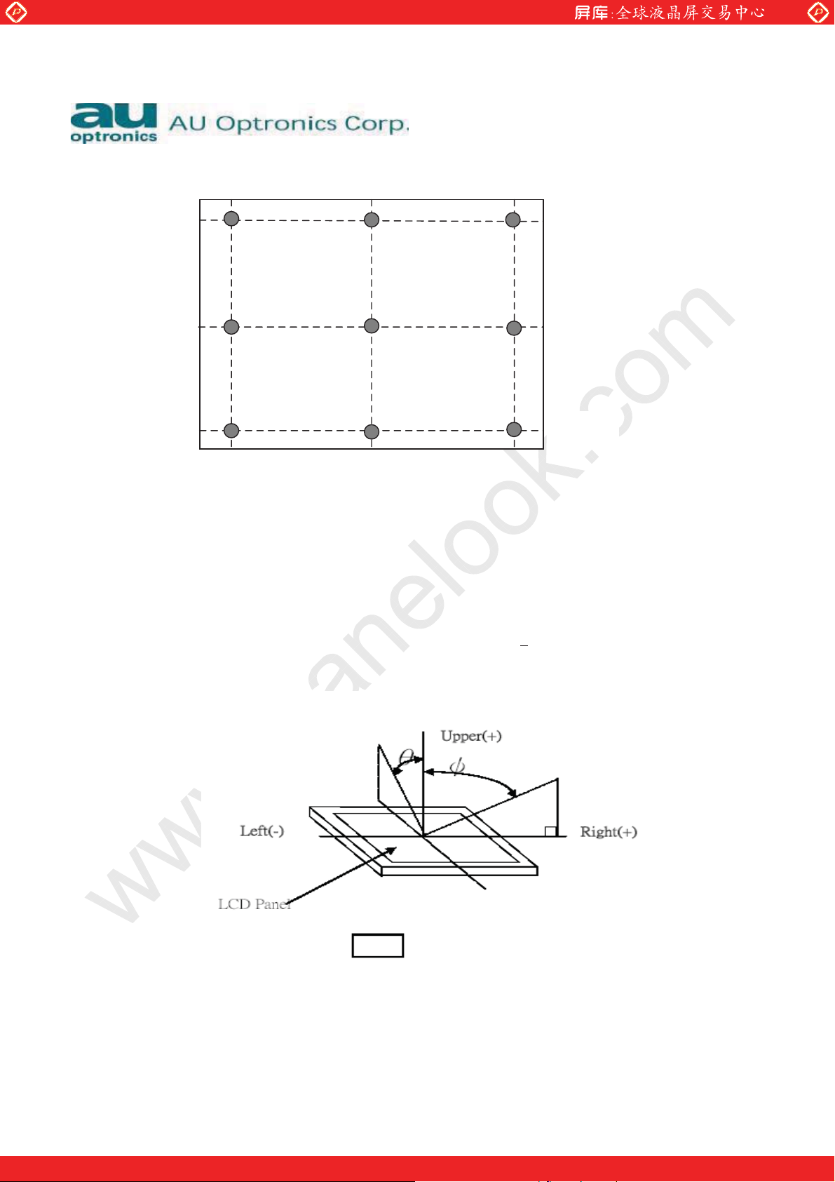
Note 2: Brightness uniformity of these 9 points is defined as below:
90 %
www.panelook.com
50 %
10 %
10 %
50 %
90 %
Minimum Luminance in 9 Points (1-9)
Uniformity = ————————————————————
Maximum Luminance in 9 Points (1-9)
Note 3: TCO ’99 Certification Requirements and test methods for environmental labeling of Display Report No. 2
defines Luminance uniformity as below:
((Lmax,+30deg. / Lmin,+30deg.) + (Lmax,-30deg. / Lmin,-30deg.)) / 2
This panel is compatible with TCO99 approbation in luminance uniformity <
Note 4: Viewing angle definition
1.7, luminance contrast >0.5
(C) Copyright AU Optronics, Inc.
January, 2002 All Rights Reserved. M170ES05 v.2 Ver0.1
No Reproduction and Redistribution Allowed.
One step solution for LCD / PDP / OLED panel application: Datasheet, inventory and accessory!
9/28
www.panelook.com
Page 10
Global LCD Panel Exchange Center
1/2
www.panelook.com
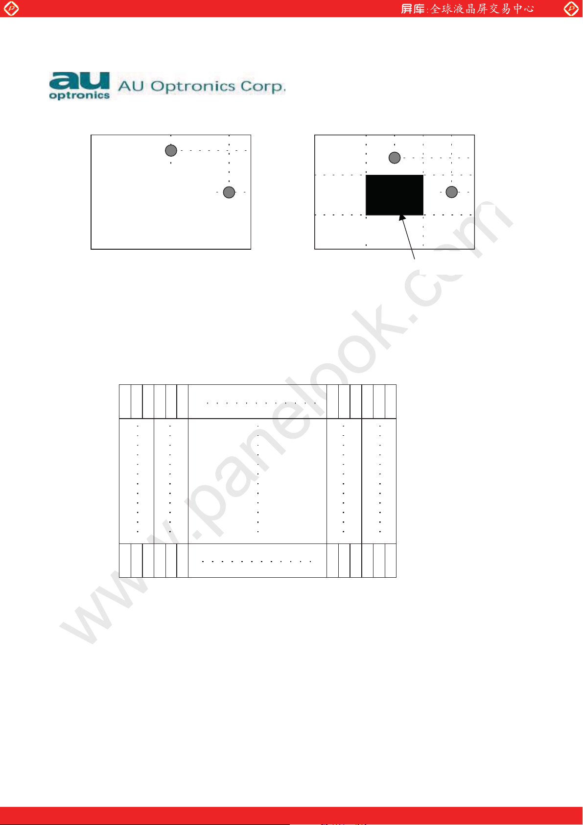
Note 5:
1/6
1/2
2/3 1/3
1/6
A
B
184 gray level 184 gray level
Unit: percentage of dimension of display area
l L
l L
l / LA x 100%= 1.5% max., LA and LB are brightness at location A and B
A-LA’
l / LB x 100%= 1.5% max., LA’ and LB’ are brightness at location A’ and B’
B-LB’
1/6
1/2
A’
2.4: Pixel format image
Following figure shows the relationship of the input signals and LCD pixel format.
1 2 1279 1280
1st Line
R G B R G B
R G B R G B
B’
0 gray level
1/6
1/3
1/2
2/3
1024th
(C) Copyright AU Optronics, Inc.
January, 2002 All Rights Reserved. M170ES05 v.2 Ver0.1
No Reproduction and Redistribution Allowed.
R G B R G B
R G B R G B
One step solution for LCD / PDP / OLED panel application: Datasheet, inventory and accessory!
10/28
www.panelook.com
Page 11
Global LCD Panel Exchange Center
p
m
idit
y
3.0 Electrical characteristics
3.1 Absolute Maximum Ratings
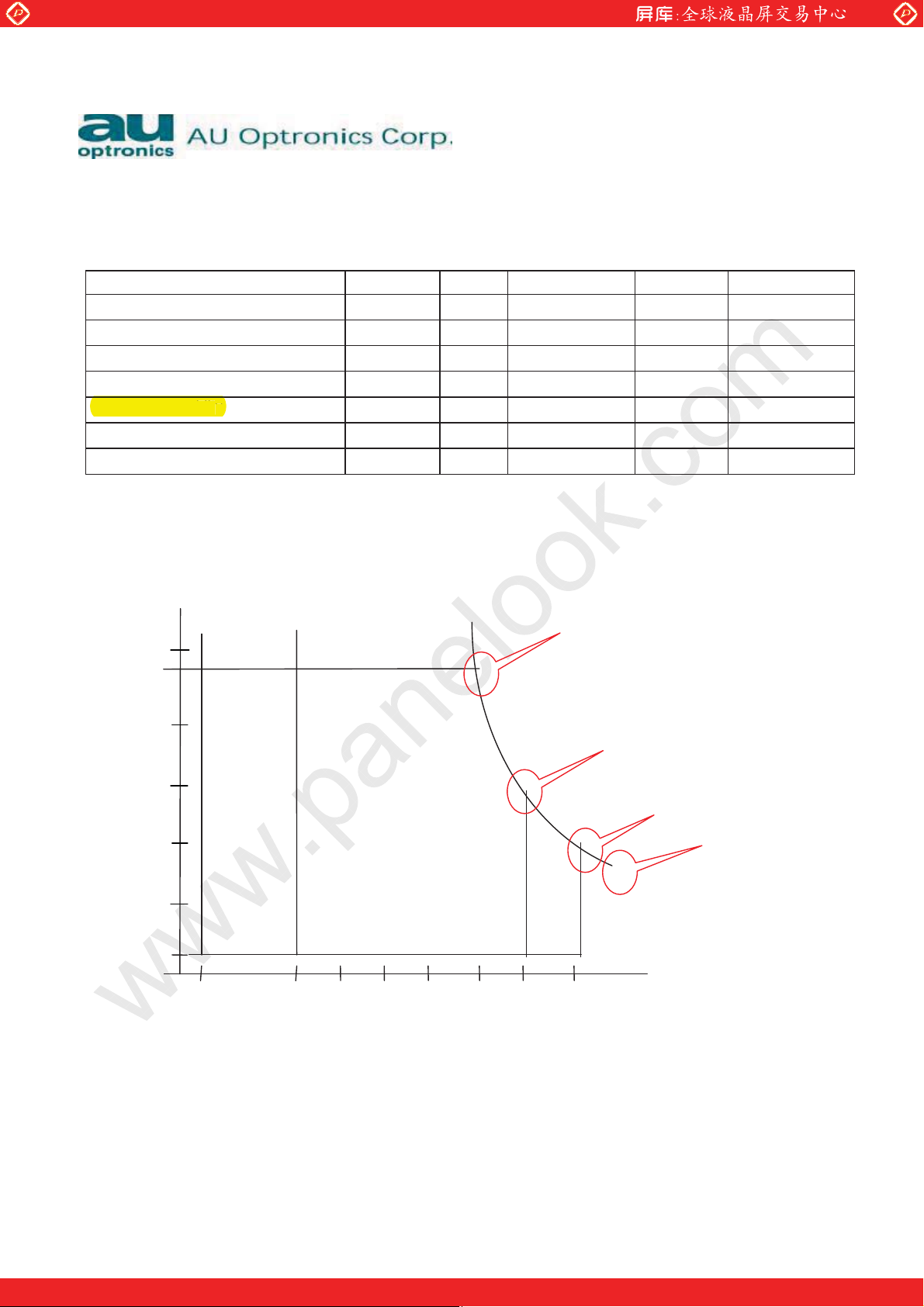
Absolute maximum ratings of the module is as following:
Item Symbol Min Max Unit Conditions
Logic/LCD Drive Voltage VIN -0.3 +5.5 [Volt]
CCFL Inrush current ICFLL - 38 [mA]
CCFL Current ICFL - 7.6 [mA] rms
Operating Temperature TOP 0 +50 [oC] Note 1
Operating Humidity HOP 8 95 [%RH] Note 1
Operating Hu
Storage Temperature TST -20 +60 [oC] Note 1
Storage Humidity HST 8 95 [%RH] Note 1
www.panelook.com
Note 1 : Maximum Wet-Bulb should be 39
Relative Humidity %
100
95
80
60
Storage
40
range
Operation range
20
5
0
-20
06050
Tem
and No condensation.
Twb=39
T=40,H=95%
T=50,H=55%
T=60,H=39%
T=65,H=29%
Storage
eratureoC
(C) Copyright AU Optronics, Inc.
January, 2002 All Rights Reserved. M170ES05 v.2 Ver0.1
No Reproduction and Redistribution Allowed.
One step solution for LCD / PDP / OLED panel application: Datasheet, inventory and accessory!
11/28
www.panelook.com
Page 12
Global LCD Panel Exchange Center
www.panelook.com
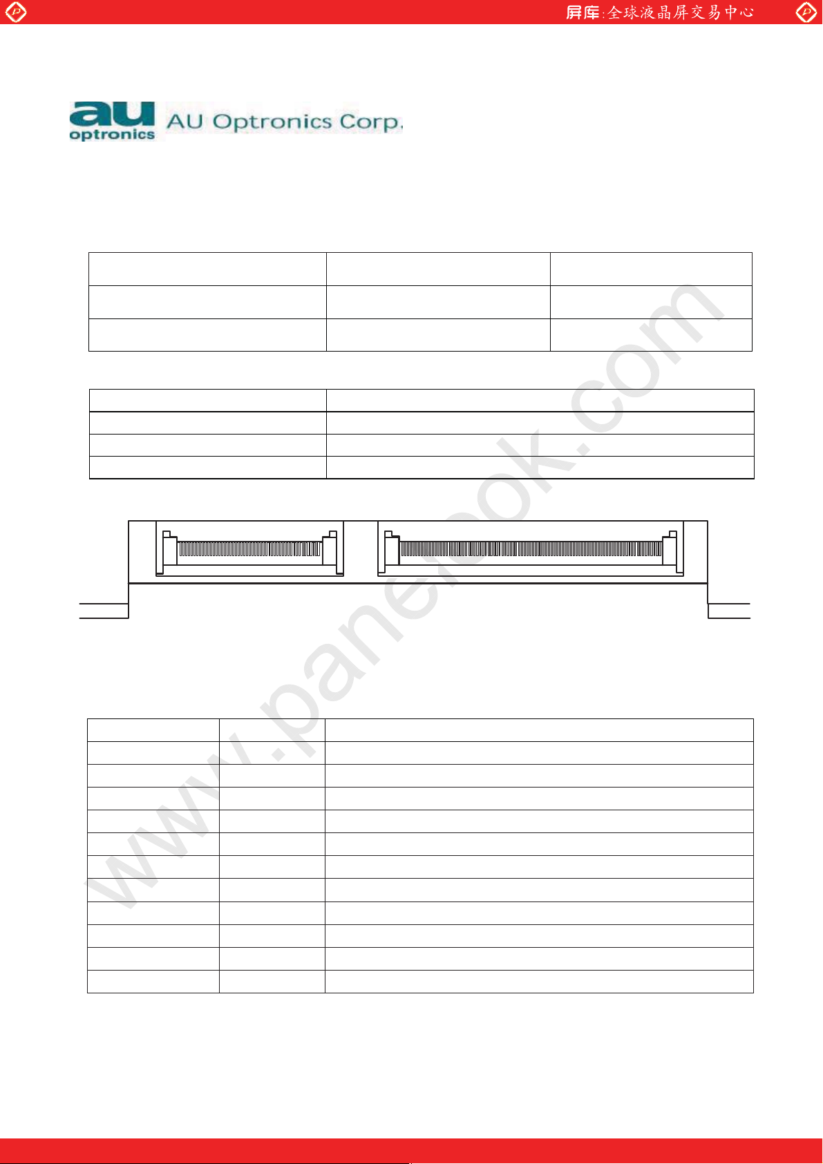
3.2 Connectors
Physical interface is described as for the connector on module.
These connectors are capable of accommodating the following signals and will be following components.
X-PCBA
Connector Name J1 J2
Manufacture
Type Part Number AF7501-A2G1T
P-TWO ()
or compatible
(FH12-50S-0.5H)
CCFL
Connector Name Lamp Connector / Backlight lamp
Manufacturer JST
Type Part Number BHR-04VS-1
Mating Type Part Number SM04(4.0)B-BHS-1-TB
Connector Diagram: Rear view of LCM
30F P-TWOP-TWO50F
#1
#30
#1 #50
J2
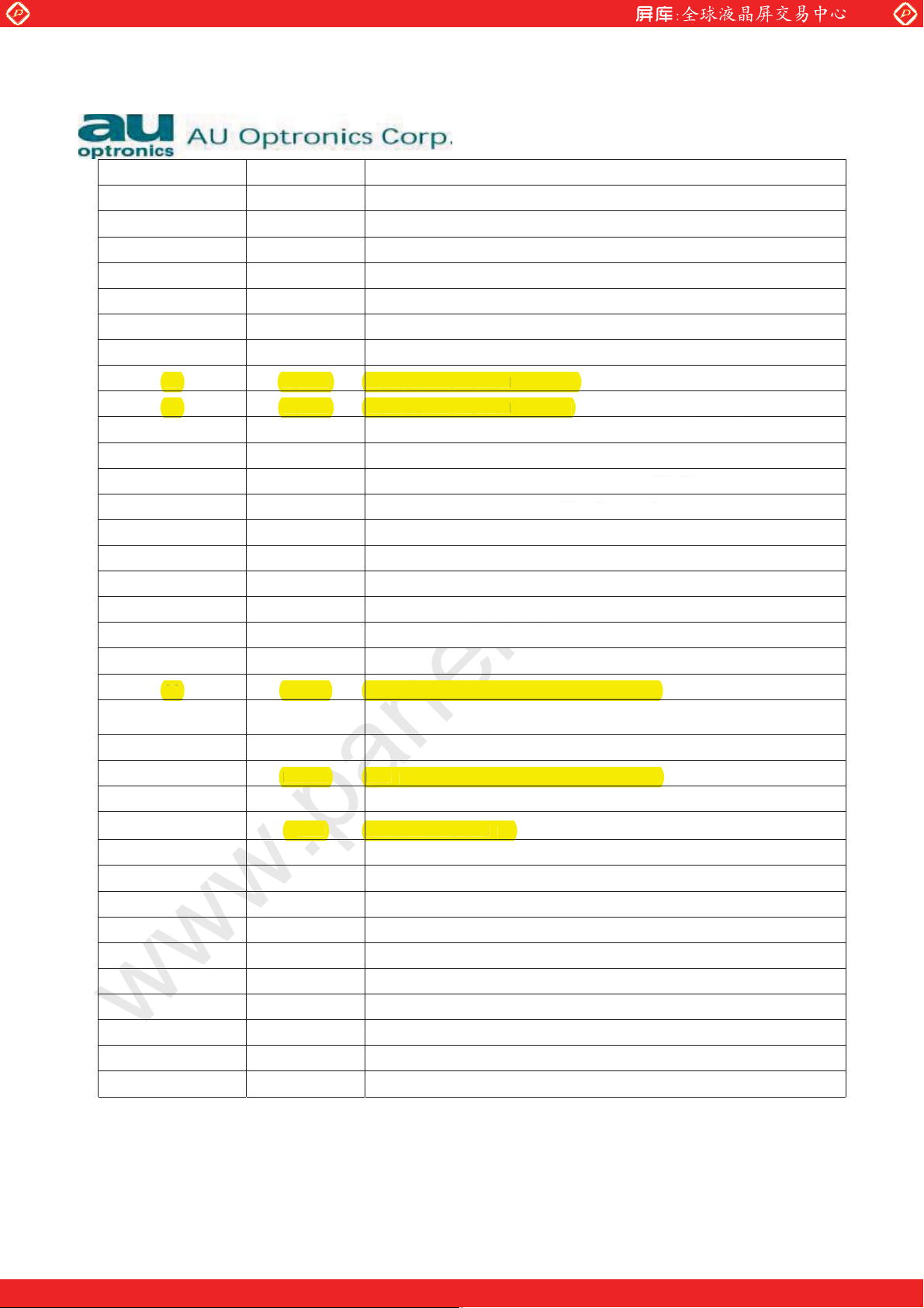
3.3 Signal Pin & Description
Connector J1
P-TWO ()
or compatible
AF7301-A2G1T
(FH12-30S-0.5H)
J1
Pin NO. Symbol Description
1 GND Ground
2 FB[0]N Front side blue RSDS signal pair 0 negative data
3 FB[0]P Front side blue RSDS signal pair 0 positive data
4 GND Ground
5 FB[1]N Front side blue RSDS signal pair 1 negative data
6 FB[1]P Front side blue RSDS signal pair 1 positive data
7 GND Ground
8 FB[2]N Front side blue RSDS signal pair 2 negative data
9 FB[2]P Front side blue RSDS signal pair 2 positive data
10 GND Ground
11 FG[0]N Front side green RSDS signal pair 0 negative data
(C) Copyright AU Optronics, Inc.
January, 2002 All Rights Reserved. M170ES05 v.2 Ver0.1
No Reproduction and Redistribution Allowed.
12/28
One step solution for LCD / PDP / OLED panel application: Datasheet, inventory and accessory!
www.panelook.com
Page 13
Global LCD Panel Exchange Center
CLK
G
20FCLKN
c
k
e
c
positive
32
O
O
12 FG[0]P Front side green RSDS signal pair 0 positive data
13 GND Ground
14 FG[1]N Front side green RSDS signal pair 1 negative data
15 FG[1]P Front side green RSDS signal pair 1 positive data
16 GND Ground
17 FG[2]N Front side green RSDS signal pair 2 negative data
18 FG[2]P Front side green RSDS signal pair 2 positive data
19 GND Ground
20 FCLKN Front side RSDS clock negative
21 FCLKP Front side RSDS clock positive
22 GND Ground
23 FR[0]N Front side red RSDS signal pair 0 negative data
24 FR[0]P Front side red RSDS signal pair 0 positive data
25 GND Ground
26 FR[1]N Front side red RSDS signal pair 1 negative data
27 FR[1]P Front side red RSDS signal pair 1 positive data
28 GND Ground
29 FR[2]N Front side red RSDS signal pair 2 negative data
30 FR[2]P Front side red RSDS signal pair 2 positive data
31 GND Ground
32 FXDIO Front side source driver IC start pulse signal
33 XSTB
34 POL Source driver IC output polarity control
35 BXDIO Back side Source driver IC start pulse signal
36 GND Ground
FCLKP Front side RSDS clo
FXDI
BXDI
www.panelook.com
Front side RSDS clo
Front side source driver IC start pulse signal
Latch the polarity of source outputs and switch the new data to source
outputs
side Source driver IC start pulse signal
negativ
37 YCLK Gate driver IC clock in
38 YDIO Gate driver IC start pulse
39 YOE Gate driver IC output enable signal
40
41
42
43
44 VDD 5V input Voltage
45 GND Ground
46 VDD 5V input Voltage
47 VDD 5V input Voltage
(C) Copyright AU Optronics, Inc.
January, 2002 All Rights Reserved. M170ES05 v.2 Ver0.1
No Reproduction and Redistribution Allowed.
NC
GND
NC
NC
ate driver IC cloc n
-
Ground
-
-
13/28
One step solution for LCD / PDP / OLED panel application: Datasheet, inventory and accessory!
www.panelook.com
Page 14
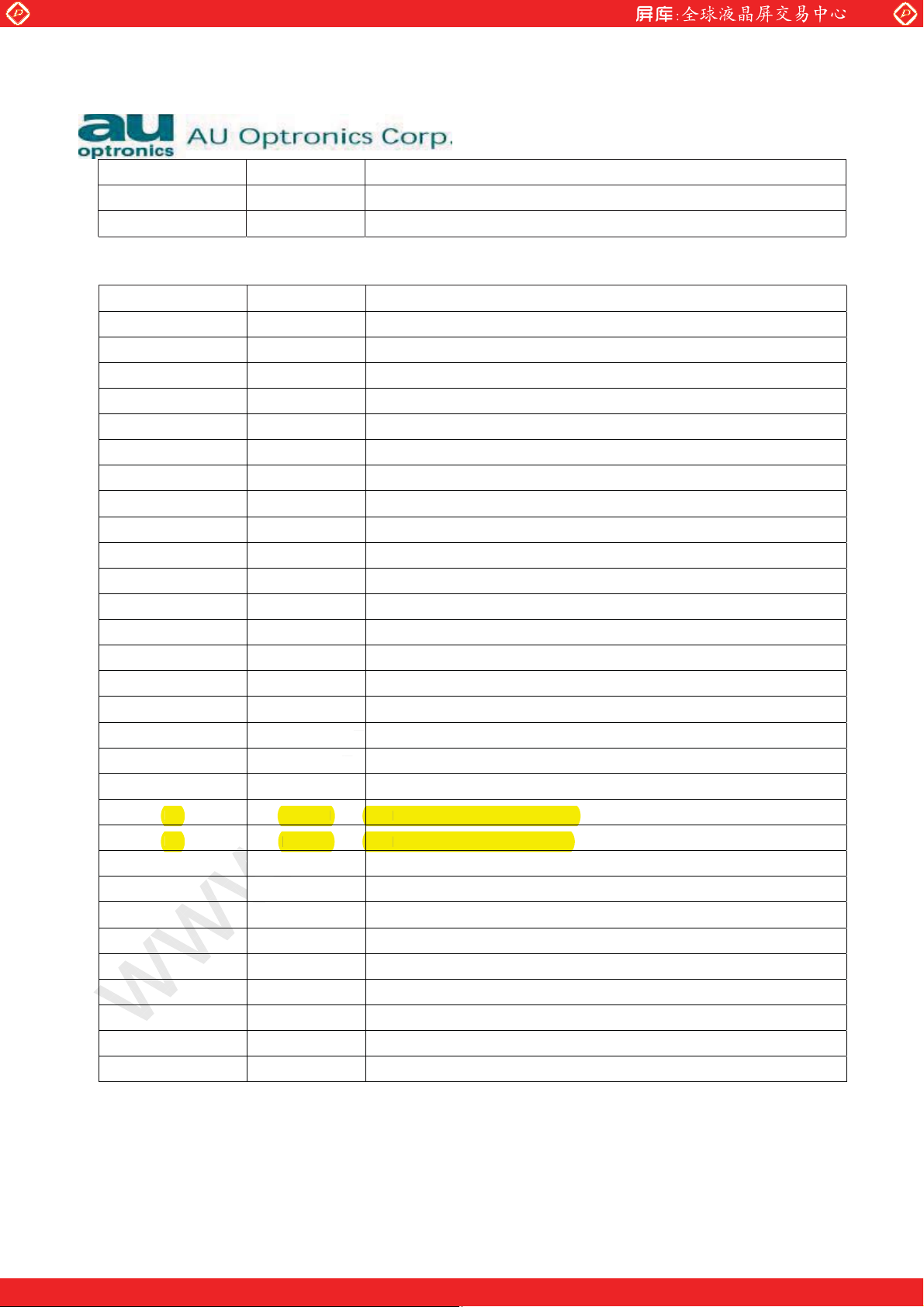
Global LCD Panel Exchange Center
48 VDD 5V input Voltage
49 ID1 Maker ID bit1 (Ground)
50 ID0 Maker ID bit0 (Ground)
Connector J2
Pin NO.
1 GND Ground
2 BB[0]N Back side blue RSDS signal pair 0 negative data
3 BB[0]P Back side blue RSDS signal pair 0 positive data
4 GND Ground
5 BB[1]N Back side blue RSDS signal pair 1 negative data
6 BB[1]P Back side blue RSDS signal pair 1 positive data
7 GND Ground
8 BB[2]N Back side blue RSDS signal pair 2 negative data
9 BB[2]P Back side blue RSDS signal pair 2 positive data
10 GND Ground
11 BG[0]N Back side green RSDS signal pair 0 negative data
12 BG[0]P Back side green RSDS signal pair 0 positive data
13 GND Ground
14 BG[1]N Back side green RSDS signal pair 1 negative data
15 BG[1]P Back side green RSDS signal pair 1 positive data
16 GND Ground
17 BG[2]N Back side green RSDS signal pair 2 negative data
18 BG[2]P Back side green RSDS signal pair 2 positive data
19 GND Ground
20 BCLKN Back side RSDS clock negative
21 BCLKP Back side RSDS clock positive
22 GND Ground
23 BR[0]N Back side red RSDS signal pair 0 negative data
24 BR[0]P Back side red RSDS signal pair 0 positive data
25 GND Ground
26 BR[1]N Back side red RSDS signal pair 1 negative data
27 BR[1]P Back side red RSDS signal pair 1 positive data
28 GND Ground
29 BR[2]N Back side red RSDS signal pair 2 negative data
30 BR[2]P Back side red RSDS signal pair 2 positive data
Symbol Description
BCLKN
BCLKP
www.panelook.com
side RSDS cloc
side RSDS cloc
negative
positive
(C) Copyright AU Optronics, Inc.
January, 2002 All Rights Reserved. M170ES05 v.2 Ver0.1
No Reproduction and Redistribution Allowed.
One step solution for LCD / PDP / OLED panel application: Datasheet, inventory and accessory!
14/28
www.panelook.com
Page 15
Global LCD Panel Exchange Center
RSDS common mode
www.panelook.com
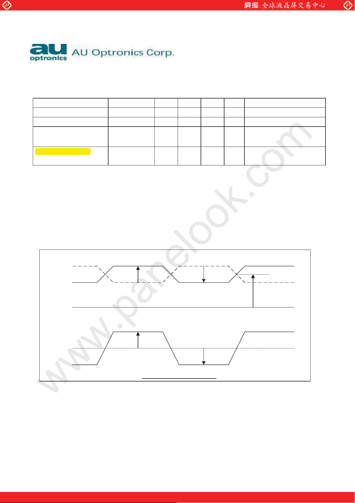
3.4 RSDS signal electrical characteristic
RSDS Characteristics
Parameter Symbol Min. Typ. Max. Unit Conditions
RSDS high input voltage VIHRSDS 100 200 - mV VCMRSDS = + 1.2 V
RSDS low input voltage VILRSDS - - 200 - 100 mV VCMRSDS = + 1.2 V
(1)
VCMRSDS
input voltage range
RSDS input leakage
IDL -10 - 10 uA
current
Notes:
1. VCMRSDS = (VCLKP + VCLKN) / 2 or VCMRSDS = (VDxxP + VDxxN) / 2
0.5 - 1.4 V
(2)
VDIFFRSDS
= 200 mV
(minimum value)
DxxP,DxxN,CLKP,CLKN
(3)
2. VDIFFRSDS = VCLKP - VCLKN or VDIFFRSDS = VDxxP - VDxxN
The typical RSDS swing level of peak to peak is 400mV.
3. DxxP/N=Differential inputs for 6-bit RGB data
CLKP/N= Differential inputs for clock data
RSDS
N
V
RSDS
V
RSDS
P
RSDS
P)-(V
RSDS
(V
N)
VIH
VIH
RSDS
VIL
VIL
RSDS
RSDS
VCM
GND
0V
RSDS
RSDS signal definition
(C) Copyright AU Optronics, Inc.
January, 2002 All Rights Reserved. M170ES05 v.2 Ver0.1
No Reproduction and Redistribution Allowed.
One step solution for LCD / PDP / OLED panel application: Datasheet, inventory and accessory!
15/28
www.panelook.com
Page 16
Global LCD Panel Exchange Center
Clock Pulse
www.panelook.com
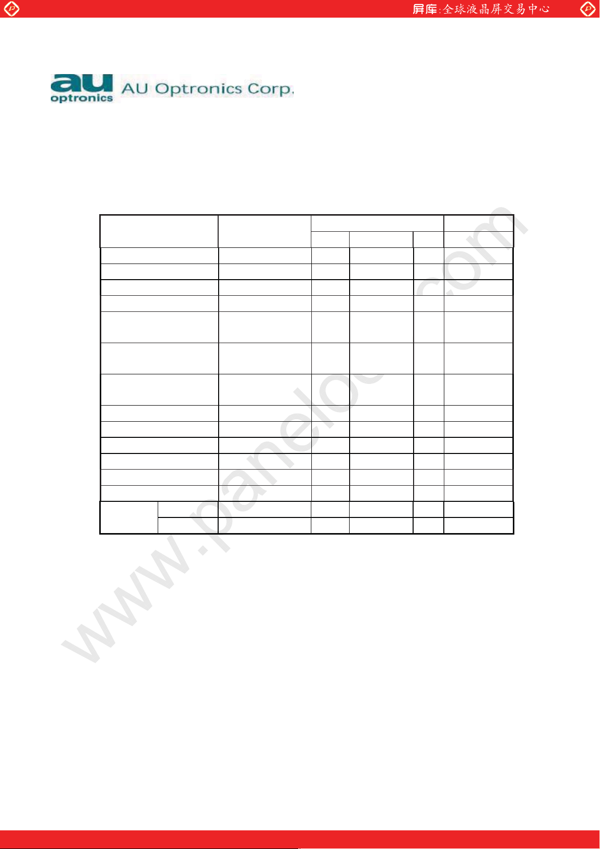
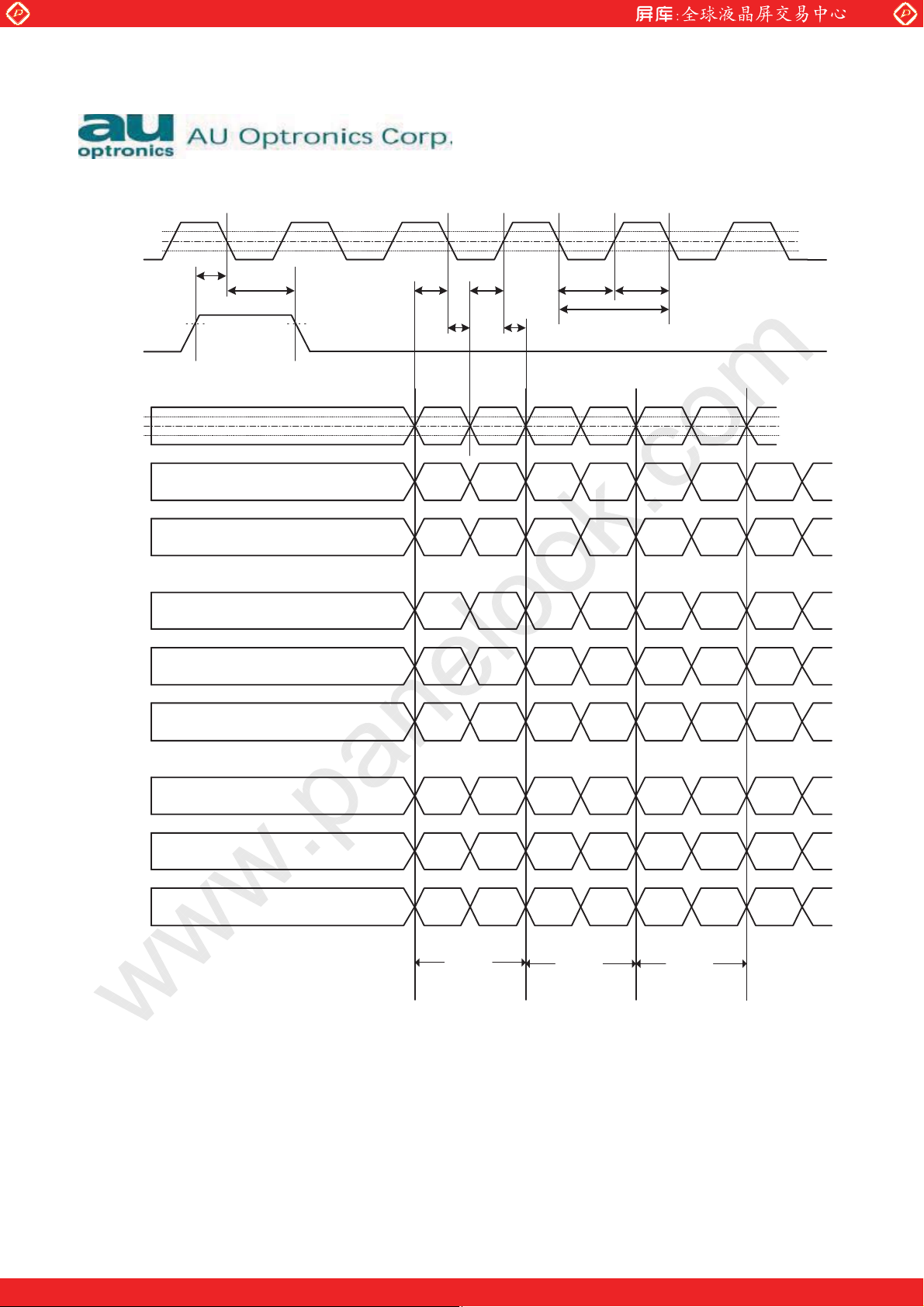
3.5 Timing Requirement
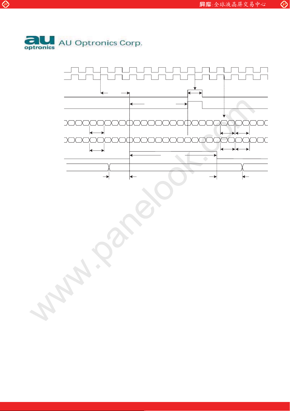
This following data describes the source and gate drivers timing requirement for 17” SXGA (12801024) Panel. The
control timing is defined based on VESA SXGA standard(non-interlaced). The symbols and timing requirement are defined in
Table 1 and Table 2. And, the timing diagrams for the source and gate drivers are shown in Figure 1 Figure 2 and Figure 3
respectively.
Source Driver IC (Horizontal Timing)
Table 1.
Item Symbol
Min. Typ. Max.
Last Data Timing TLDT 1 14 - CLKPperiod
XDIO Pulse Width PWXDIO 1 1.6 2 CLKPperiod
XSTB-XDIO Time TSTB-XDIO 5 92 - CLKPperiod
XSTB Pulse Width PWSTB 5(?) 80 - CLKPperiod
POL-XSTB Time TPOL-STB 14 (15
XSTB-XPOL Time TSTB-POL 10 (11
XSTB-CLK Time TSTB(90%)-CLKP-N
(50%)
4 -ns
XDIO setup time TSETUP2 2--ns
XDIO hold time THOLD2 4--ns
Data setup time TSETUP1 3--ns
Data hold time THOLD1 1--ns
Clock pulse low period PWCLK(L) 6 - - ns
Clock pulse high period PWCLK(H) 6 - - ns
Frequency FCLK 40 54 67.5 MHz
width
Period PWCLK 14.81 18.52 20 ns
- Unit
- ns(CLKPperiod)
CLKPperiod)
- ns(CLKPperiod)
CLKPperiod)
(C) Copyright AU Optronics, Inc.
January, 2002 All Rights Reserved. M170ES05 v.2 Ver0.1
No Reproduction and Redistribution Allowed.
One step solution for LCD / PDP / OLED panel application: Datasheet, inventory and accessory!
16/28
www.panelook.com
Page 17
Global LCD Panel Exchange Center
FCLKP-FCLKN
BCLKP-BCLKN
www.panelook.com
FXDIO
BXDIO
FR[X]P-FR[X]N
FG[X]P-FG[X]N
FB[X]P-FB[X]N
BR[X]P-BR[X]N
BG[X]P-BG[X]N
BB[X]P-BB[X]N
XSTB
POL
Even
638
Invalid
Odd
Even
639
638
640th
Data
EvenEven
Odd Odd
1279
127912781278
1280th
Data
Odd
639
T
LDT
POL-STB
T
T
STB-XDIO
Figure 1
PW
PW
STB
XDIO
0
1st
Data
641th
Data
Even Even
Odd
0
EvenEven
1
2nd
Data
642th
Data
212
Even
Even
640 640 641 641 642 642
InvalidValid
T
STB-POL
OddOdd
OddOddOdd
(C) Copyright AU Optronics, Inc.
January, 2002 All Rights Reserved. M170ES05 v.2 Ver0.1
No Reproduction and Redistribution Allowed.
One step solution for LCD / PDP / OLED panel application: Datasheet, inventory and accessory!
17/28
www.panelook.com
Page 18
Global LCD Panel Exchange Center
www.panelook.com
CLKP-CLKN
(RSDS)
XDIO
R(0)P
-
R(0)N
R(1)P
-
R(1)N
R(2)P
-
R(2)N
G(0)P
-
G(0)N
G(1)P
-
G(1)N
T
SETUP2
T
90% 90%
HOLD2
SETUP1
T
SETUP1
T
T
HOLD1
R(0) R(1)
R(2) R(3)
R(4) R(5)
G(0)
G(2)
T
HOLD1
G(1)
G(3)
PWCLK(L) PWCLK(H)
PWCLK
R(0) R(1)
R(2) R(3)
R(4) R(5)
G(0) G(1)
G(2) G(3)
R(0) R(1)
R(2) R(3)
R(4) R(5)
G(0)
G(2) G(3)
G(1)
R(2)
R(4)
G(0)
G(2)
VIH
VCM
VIL
VIH
VCM
VIL
RSDS
RSDS
RSDS
RSDS
RSDS
RSDS
G(2)P
-
G(4)
G(5)
G(4) G(5)
G(2)N
B(0)P
-
B(0) B(1)
B(0) B(1)
B(0)N
B(1)P
-
B(2)
B(3)
B(2)
B(1)N
B(2)P
-
B(4) B(5)
B(4) B(5)
B(2)N
1st
Data
2nd
Data
Figure 2
(C) Copyright AU Optronics, Inc.
January, 2002 All Rights Reserved. M170ES05 v.2 Ver0.1
No Reproduction and Redistribution Allowed.
B(3)
G(4) G(5)
B(0)
B(2) B(3)
B(4) B(5)
B(1)
3rd
Data
G(4)
B(0)
B(2)
B(4)
(0): LSB
(6): MSB
18/28
One step solution for LCD / PDP / OLED panel application: Datasheet, inventory and accessory!
www.panelook.com
Page 19
Global LCD Panel Exchange Center
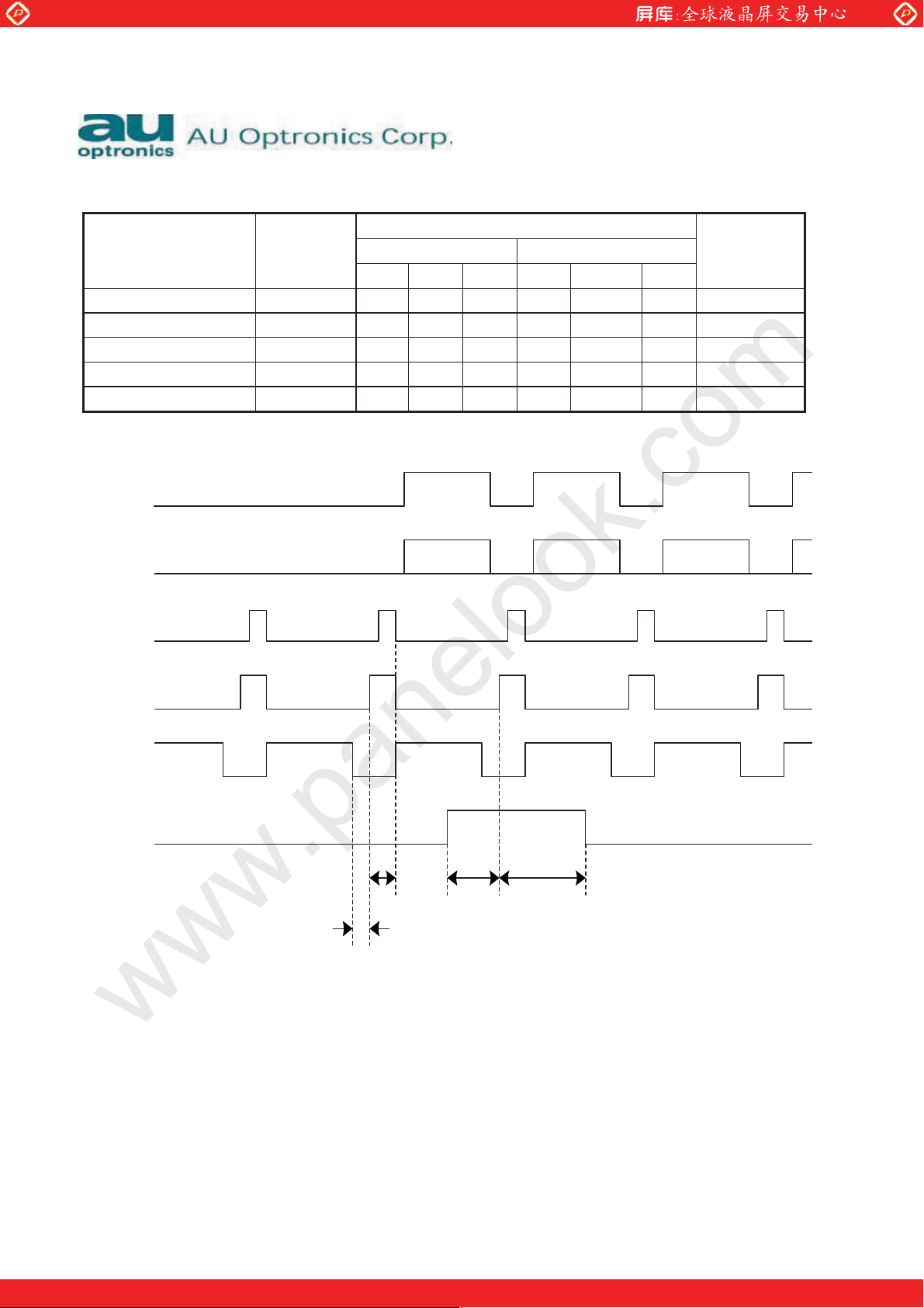
Gate Driver IC (Vertical Timing)
Item Symbol
YDIO setup time TSDI 200 6640 - 200 5280 - ns
YDIO hold time THDI 350 9040 - 350 7200 - ns
Gate off time TGOFF - 1846 - - 1470 - ns
Gate delay time TGDLY - 282 - - 242 - ns
YOE low period TGOFF+TGDLY 1000 2128 - 1000 1712 - ns
www.panelook.com
Table 2.
-
Frame rate@60Hz Frame rate@75Hz
Min. Typ. Max. Min. Typ. Max.
Unit
DE
Data
XSTB
YCLK
YOE
YDIO
Line 1 Line 2 Line 3
T
GOFF
T
SDI
T
HDI
T
GDLY
Table 3
Note1 : DE is reference signal, DE means the display data valid.
(C) Copyright AU Optronics, Inc.
January, 2002 All Rights Reserved. M170ES05 v.2 Ver0.1
No Reproduction and Redistribution Allowed.
One step solution for LCD / PDP / OLED panel application: Datasheet, inventory and accessory!
19/28
www.panelook.com
Page 20
Global LCD Panel Exchange Center
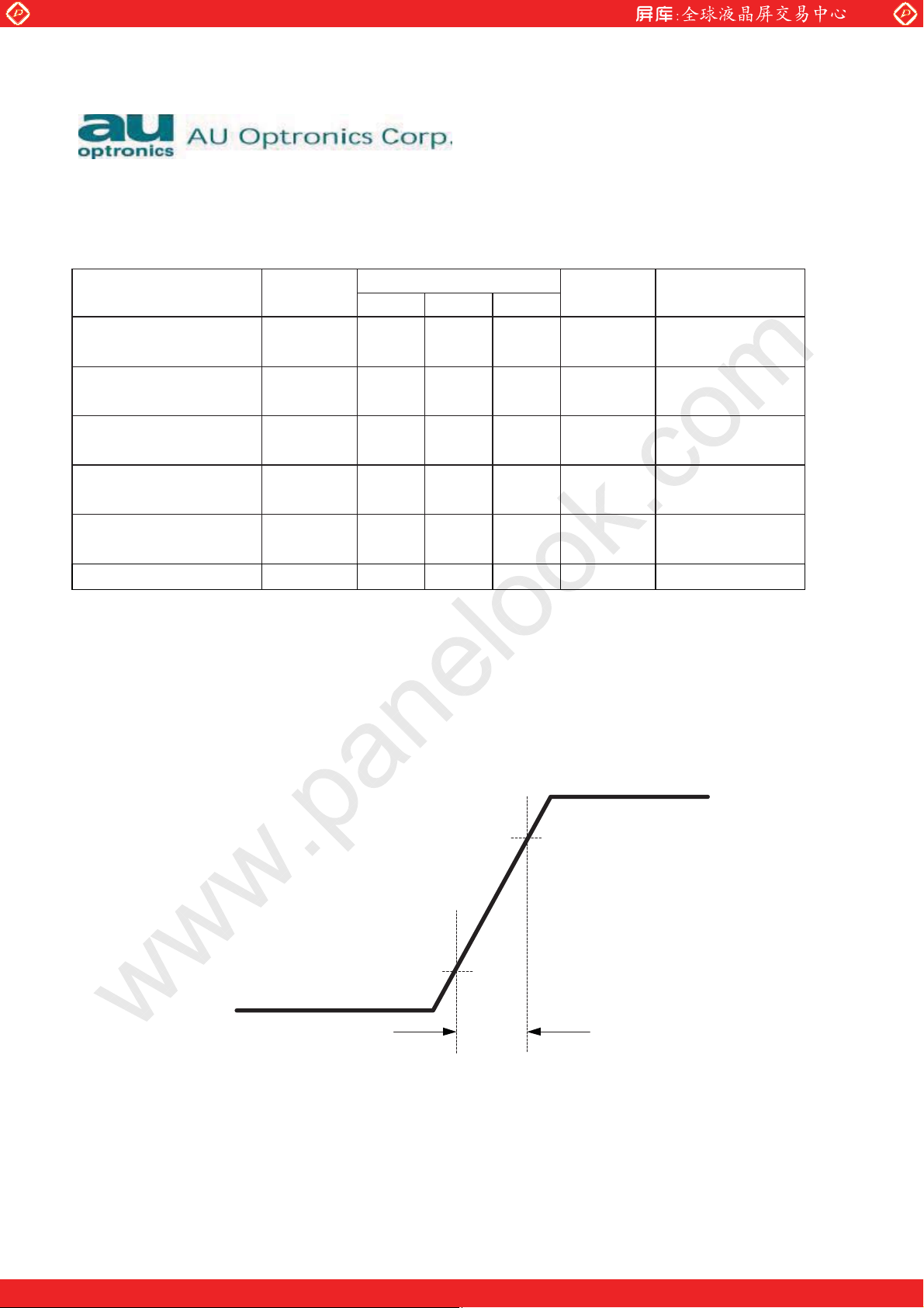
3.6 Electrical Ratings
www.panelook.com
Item Symbol
Power Supply Input
Voltage Voltage (1)
Power Supply Ripple - - 250 mVp-p
Power Supply Input
Current
Differential pair
Impedance Current
Power Consumption Pc 4 5 W 1
Inrush current Irush - - 5 A3
Notes:
1. The specified current and power consumption are under the conditions (VDD=5V,T=25
rate=75Hz,black pattern).
2. This value is needed to a proper signal quality and is measured from Scalar Chip output pins to its
mating connector. Besides, the impedance of FPC between scalar board and LCD panel is also needed
to keep.
3. Based on AU circuit design ,the duration of the rush current is about 1 ms, which should have the
following typical condition.
VDD 4.5 5 5.5 V(DC)
Icc - 800 1000 mA 1
Zm 90 100 110 Ohm 2
Min Typ Max
Values
Unit Notes
,Frame
0.9Vcc
0.1Vcc
GND
(C) Copyright AU Optronics, Inc.
January, 2002 All Rights Reserved. M170ES05 v.2 Ver0.1
No Reproduction and Redistribution Allowed.
5V
20/28
One step solution for LCD / PDP / OLED panel application: Datasheet, inventory and accessory!
www.panelook.com
Page 21
Global LCD Panel Exchange Center
www.panelook.com
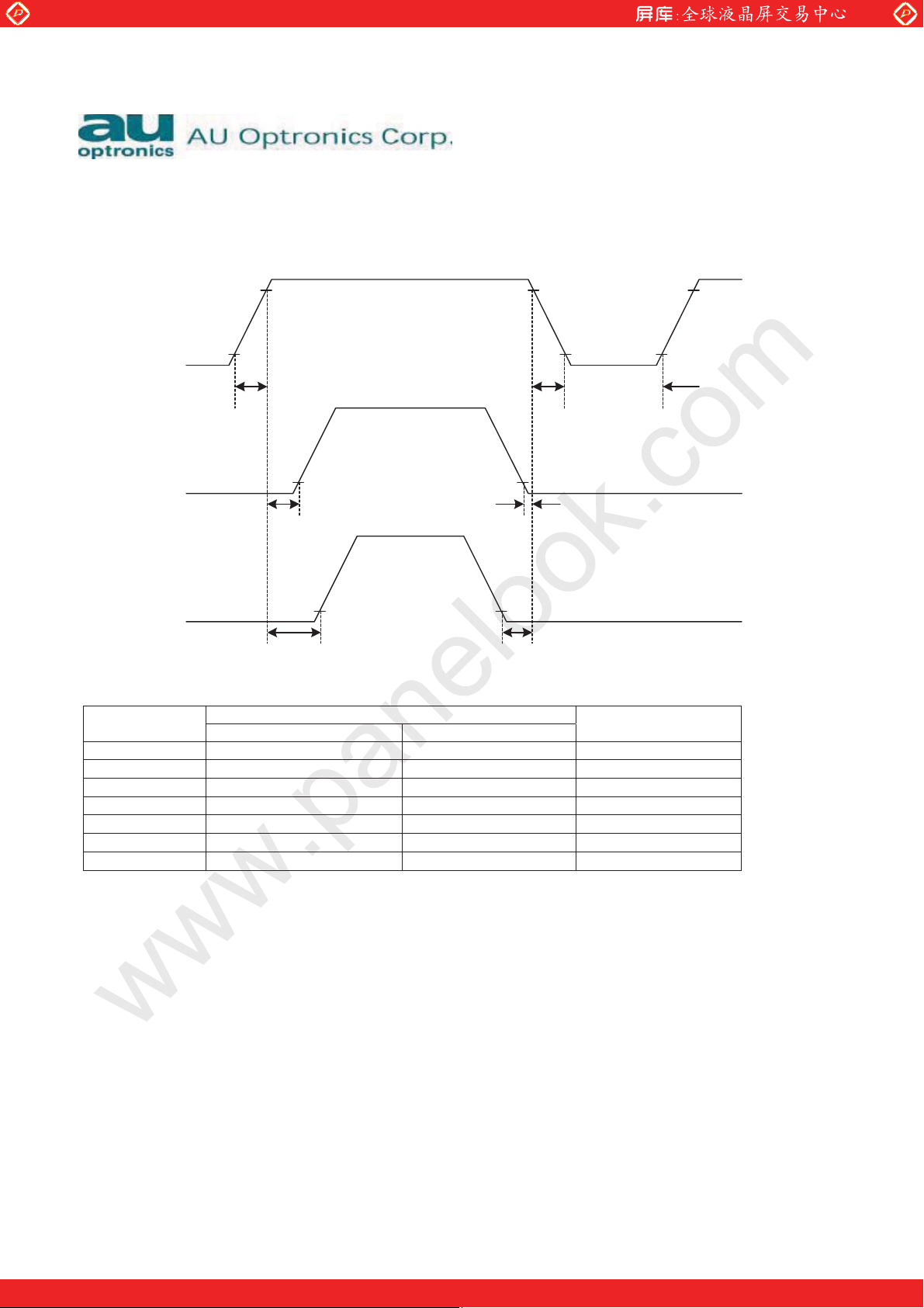
3.7 Power ON/OFF Sequence
The LCD module must be powered up and down as indicated or the device may be damaged permanently.
The power-on includes both system starting and from the sleep to wake-up mode ; the power-off includes
both system shunt down and the one from on to sleep. There should be no power sequence changing in the
sleep to wake-up mode.
90%
10%
90%
10%
VDD
T1
T6
10%10%
Signal
T5
T2
10% 10%
Lamp on
T3 T4
Parameter
T1 0.5 10 ms
T2
T3
T4
T5
T6
T7
Min Max
0.01 30
170 100 -
0-
--
1000 -
Values
T7
Unit
ms
ms
ms
ms
ms
ms
(C) Copyright AU Optronics, Inc.
January, 2002 All Rights Reserved. M170ES05 v.2 Ver0.1
No Reproduction and Redistribution Allowed.
One step solution for LCD / PDP / OLED panel application: Datasheet, inventory and accessory!
21/28
www.panelook.com
Page 22
Global LCD Panel Exchange Center
1700 voltage
p
4.0 Backlight Characteristics
4.1 Signal for Lamp connector
Pin # Signal Name
1 Lamp High Voltage
www.panelook.com
2
3
4
Lamp High Voltage
No Connection
Ground
4.2 Parameter guide line for CFL Inverter
Symbol Parameter Min Typ Max Units Condition
(L63) White Luminance 230 300 - [cd/m2] (Ta=25oC)
ISCFL CCFL standard current 6.5 7.0 7.5 [mA]
rms
IRCFL CCFL operation range 3.0 7.0 7.5 [mA]
rms
fCFL CCFL Frequency 40 50 80 [KHz] (Ta=25oC)
ViCFL
o
C)
(0
ViCFL
o
C)
(25
VCFL CCFL Discharge Voltage
CCFL Ignition Voltage 1700 [Volt]
rms
CCFL Ignition Voltage 1200 [Volt]
rms
700 860 [Volt]
(Reference)
rms
(Ta=25oC)
(Ta=25oC)
Note 1
o
(Ta=0
C)
Note 2
(Ta=25
o
C)
Note 2
(Ta=25oC)
Note 3
PCFL CCFL Power consumption 19.6 25.8 [Watt] (Ta=25oC)
Note 3
Note 1: CCFL Frequency should be carefully determined to avoid interference between inverter and TFT LCD
Note 2: CCFL inverter should be able to give out a power that has a generating capacity of over 1700 voltage.
Lamp units need 1700 voltage minimum for ignition
Note 3: Calculator value for reference (ICFL×VCFL=PCFL)
(C) Copyright AU Optronics, Inc.
January, 2002 All Rights Reserved. M170ES05 v.2 Ver0.1
No Reproduction and Redistribution Allowed.
One step solution for LCD / PDP / OLED panel application: Datasheet, inventory and accessory!
22/28
www.panelook.com
Page 23
Global LCD Panel Exchange Center
5.0 Vibration, Shock, and Drop
5.1 Vibration & Shock
Frequency: 10 - 200Hz
Sweep: 30 Minutes each Axis (X, Y, Z)
Acceleration: 1.5G(10~200Hz P- P)
Test method:
www.panelook.com
Acceleration (G)
Frequency (Hz)
Active time(min)
1.5
10~200~10
30
5.2 Shock Test Spec:
Acceleration (G)
Active time
Wave form
Times
Direction: X , Y, Z
50
20
half-sin
1
5.3 Drop test
Package test: The drop height is 60 cm.
6.0 Environment
The display module will meet the provision of this specification during operating condition or after storage or
shipment condition specified below. Operation at 10% beyond the specified range will not cause physical
damage to the unit.
6.1 Temperature and Humidity
6.1.1 Operating Conditions
The display module operates error free, when operated under the following conditions;
Temperature 0
Relative Humidity 8% to 95%
Wet Bulb Temperature 39.0
(C) Copyright AU Optronics, Inc.
January, 2002 All Rights Reserved. M170ES05 v.2 Ver0.1
No Reproduction and Redistribution Allowed.
One step solution for LCD / PDP / OLED panel application: Datasheet, inventory and accessory!
0
C to 50 0C
0
C
23/28
www.panelook.com
Page 24
Global LCD Panel Exchange Center
6.1.2 Shipping Conditions
The display module operates error free, after the following conditions;
Temperature -20
Relative Humidity 8% to 95%
Wet Bulb Temperature 39.0
6.2 Atmospheric Pressure
The display assembly is capable of being operated without affecting its operations over the pressure range
as following specified;
Maximum Pressure 1040hPa 0m = sea level
Minimum Pressure 674hPa 3048m = 10.000 feet
www.panelook.com
0
C to 60 0C
0
C
Pressure Note
Note : Non-operation attitude limit of this display module = 30,000 feet. = 9145 m.
6.3 Thermal Shock
The display module will not sustain damage after being subjected to 100 cycles of rapid temperature
change. A cycle of rapid temperature change consists of varying the temperature from -20
back again.
0
Thermal shock cycle -20
C for 30min
0
C for 30min
60
Power is not applied during the test. After temperature cycling, the unit is placed in normal room ambient for
at least 4 hours before powering on.
0
C to 600C, and
7.0 Reliability
This display module and the packaging of that will comply following standards.
7.1 Failure Criteria
The display assembly will be considered as failing unit when it no longer meets any of the requirements
stated in this specification. Only as for maximum white luminance, following criteria is applicable.
2
Note : Maximum white Luminance shall be 125 cd/m
or more.
7.2 Failure Rate
The average failure rate of the display module (from first power-on cycle till 1,000 hours later) will not exceed 1.0%.
The average failure rate of the display module from 1,000 hours until 16,000 hours will not exceed 0.7%
per 1000 hours.
(C) Copyright AU Optronics, Inc.
January, 2002 All Rights Reserved. M170ES05 v.2 Ver0.1
No Reproduction and Redistribution Allowed.
One step solution for LCD / PDP / OLED panel application: Datasheet, inventory and accessory!
24/28
www.panelook.com
Page 25
Global LCD Panel Exchange Center
7.2.1 Usage
The assumed usage for the above criteria is:
220 power-on hours per month
500 power on/off cycles per month
Maximum brightness setting
Operation to be within office environment (25
7.2.2 Component De-rating
All the components used in this device will be checked the load condition to meet the failure rate criteria.
7.3 CCFL Life
The assumed CCFL Life will be longer than 30,000 hours, typical value is 40,000 hours under stable condition at 25
o
C;
± 5
Standard current at 7.0 ± 0.5mA.
Definition of life: brightness becomes 50% or less than the minimum luminance value of CCFL.
www.panelook.com
0
C typical)
7.4 ON/OFF Cycle
The display module will be capable of being operated over the following ON/OFF Cycles.
ON/OFF Value Cycles
+Vin and CCFL power 30,000 10 seconds on / 10 seconds off
8.0 Safety
8.1 Sharp Edge Requirements
There will be no sharp edges or comers on the display assembly that could cause injury.
8.2 Materials
8.2.1 Toxicity
There will be no carcinogenic materials used anywhere in the display module. If toxic materials are used,
they will be reviewed and approved by the responsible AU Toxicologist.
8.2.2 Flammability
All components including electrical components that do not meet the flammability grade UL94-V1 in the
module will complete the flammability rating exception approval process. The printed circuit board will be
made from material rated 94-V1 or better. The actual UL flammability rating will be printed on the printed
circuit board.
(C) Copyright AU Optronics, Inc.
January, 2002 All Rights Reserved. M170ES05 v.2 Ver0.1
No Reproduction and Redistribution Allowed.
One step solution for LCD / PDP / OLED panel application: Datasheet, inventory and accessory!
25/28
www.panelook.com
Page 26
Global LCD Panel Exchange Center
8.3 Capacitors
If any polarized capacitors are used in the display assembly, provisions will be made to keep them from
being inserted backwards.
8.4 Hazardous Voltages
Any point exceeding 42.4 volts meets the requirement of the limited current circuit. The current through a 2K
resistance is less than 0.7 x f (kHz) mA.
www.panelook.com
9.0 Other requirements
9.1 National Test Lab Requirement
The display module will satisfy all requirements for compliance to
UL 1950, First Edition U.S.A. Information Technology Equipment
CSA C22.2 No.950-M89 Canada, Information Technology Equipment
EEC 950 International, Information Technology Equipment
EN 60 950 International, Information Processing Equipment
(European Norm for IEC950)
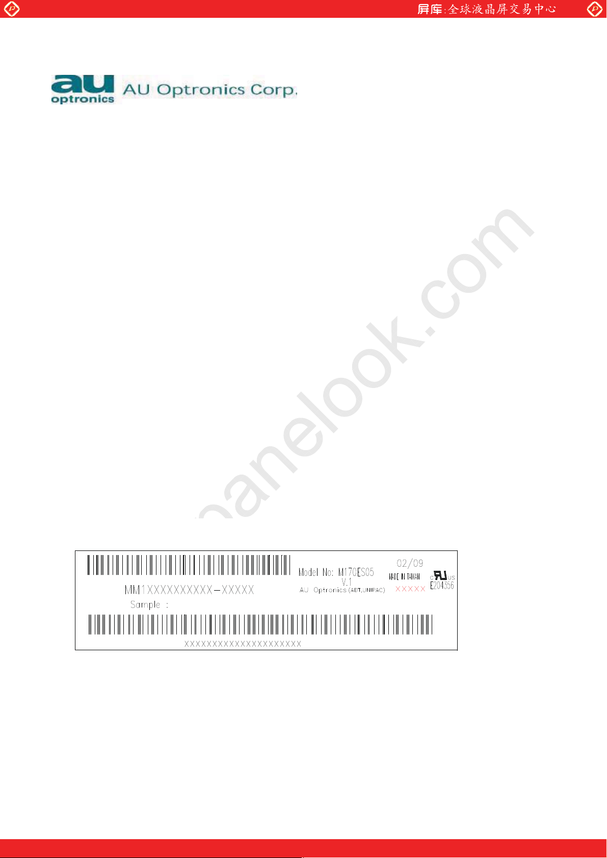
9.2 Label
9.2.1 Product label
(C) Copyright AU Optronics, Inc.
January, 2002 All Rights Reserved. M170ES05 v.2 Ver0.1
No Reproduction and Redistribution Allowed.
One step solution for LCD / PDP / OLED panel application: Datasheet, inventory and accessory!
26/28
www.panelook.com
Page 27
Global LCD Panel Exchange Center
www.panelook.com
27/28
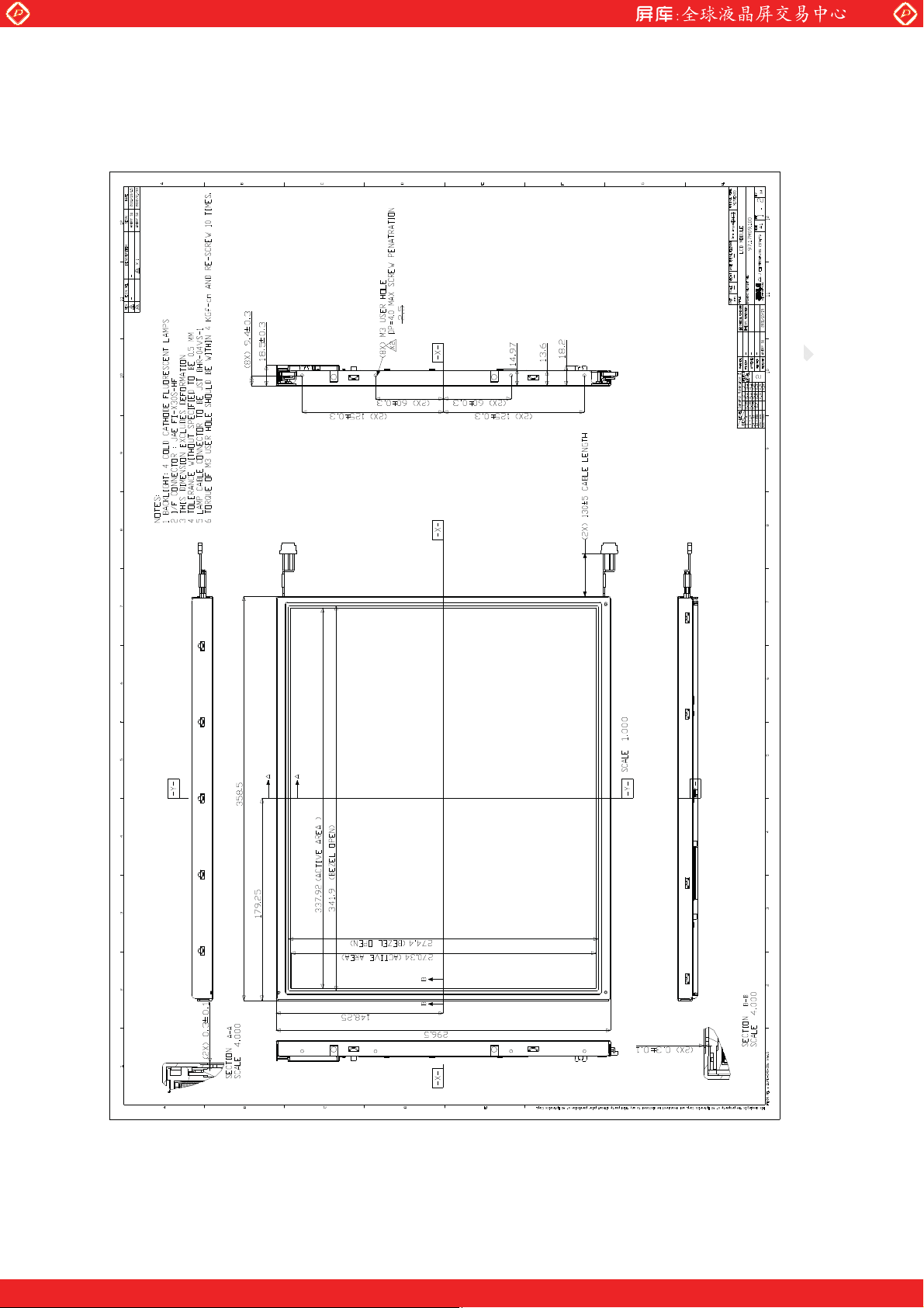
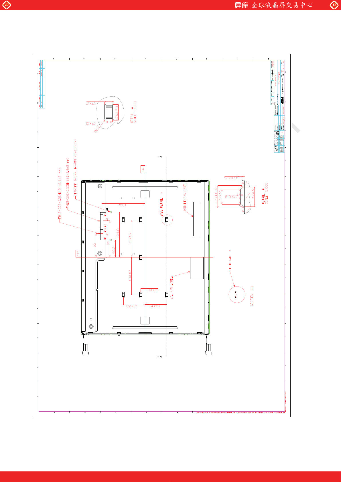
10.0 Mechanical Characteristics
One step solution for LCD / PDP / OLED panel application: Datasheet, inventory and accessory!
(C) Copyright AU Optronics, Inc.
January, 2002 All Rights Reserved. M170ES05 v.2 Ver0.1
No Reproduction and Redistribution Allowed.
www.panelook.com
Page 28
Global LCD Panel Exchange Center
www.panelook.com
28/28
One step solution for LCD / PDP / OLED panel application: Datasheet, inventory and accessory!
(C) Copyright AU Optronics, Inc.
January, 2002 All Rights Reserved. M170ES05 v.2 Ver0.1
No Reproduction and Redistribution Allowed.
www.panelook.com
 Loading...