

Page 1
Global LCD Panel Exchange Center
www.panelook.com
Product Functional Specification
15 inch XGA Color TFT LCD Module
Model Name : B150XG01 V.7
() Preliminary Specification
( ) Final Specification
Note: This Specification is subject to change without notice.
(C) Copyright AU Optronics, Inc.
August, 2001 All Rights Reserved. B150XG01 V7 Ver.01
No Reproduction and Redistribution Allowed.
One step solution for LCD / PDP / OLED panel application: Datasheet, inventory and accessory!
1/19
www.panelook.com
Page 2
Global LCD Panel Exchange Center
I. Contents
1.0 Handling Precautions
2.0 General Description
2.1 Characteristics
2.2 Functional Block Diagram
3.0 Absolute Maximum Ratings
4.0 Optical Characteristics
5.0 Signal Interface
5.1 Connectors
5.2 Signal Pin
www.panelook.com
5.3 Signal Description
5.4 Signal Electrical Characteristics
5.5 Signal for Lamp Connector
6.0 Pixel Format Image
7.0 Parameter Guide Line for CFL Inverter
8.0 Interface Timings
8.1 Timing Characteristics
8.2 Timing Definition
9.0 Power Consumption
10.0 Power ON/OFF Sequence
11.0 Mechanical Characteristics
II Record of Revision
Version and Date Page Old description New Description Remark
0.1. 2005/3/3 All First release All
(C) Copyright AU Optronics, Inc.
August, 2001 All Rights Reserved. B150XG01 V7 Ver.01
No Reproduction and Redistribution Allowed.
One step solution for LCD / PDP / OLED panel application: Datasheet, inventory and accessory!
2/19
www.panelook.com
Page 3

Global LCD Panel Exchange Center
www.panelook.com
1.0 Handing Precautions
1) Since front polarizer is easily damaged, pay attention not to scratch it.
2) Be sure to turn off power supply when inserting or disconnecting from input connector.
3) Wipe off water drop immediately. Long contact with water may cause discoloration or
spots.
4) When the panel surface is soiled, wipe it with absorbent cotton or other soft cloth.
5) Since the panel is made of glass, it may break or crack if dropped or bumped on hard
surface.
6) Since CMOS LSI is used in this module, take care of static electricity and insure
human earth when handling.
7) Do not open nor modify the Module Assembly.
8) Do not press the reflector sheet at the back of the module to any directions.
9) In case if a Module has to be put back into the packing container slot after once it was
taken out from the container, do not press the center of the CCFL Reflector edge.
Instead, press at the far ends of the CFL Reflector edge softly. Otherwise the TFT
Module may be damaged.
10) At the insertion or removal of the Signal Interface Connector, be sure not to rotate nor
tilt the Interface Connector of the TFT Module.
11) After installation of the TFT Module into an enclosure (Notebook PC Bezel, for
example), do not twist nor bend the TFT Module even momentary. At designing the
enclosure, it should be taken into consideration that no bending/twisting forces are
applied to the TFT Module from outside. Otherwise the TFT Module may be damaged.
12) Cold cathode fluorescent lamp in LCD contains a small amount of mercury. Please follow
local ordinances or regulations for disposal.
13) Small amount of materials having no flammability grade is used in the LCD module. The
LCD module should be supplied by power complied with requirements of Limited Power
Source(2.11, IEC60950 or UL1950), or be applied exemption.
14) The LCD module is designed so that the CFL in it is supplied by Limited Current Circuit(2.4,
IEC60950 or UL1950). Do not connect the CFL in Hazardous Voltage Circuit.
(C) Copyright AU Optronics, Inc.
August, 2001 All Rights Reserved. B150XG01 V7 Ver.01
No Reproduction and Redistribution Allowed.
One step solution for LCD / PDP / OLED panel application: Datasheet, inventory and accessory!
3/19
www.panelook.com
Page 4

Global LCD Panel Exchange Center
www.panelook.com
2.0 General Description
This specification applies to the 15.0 inch Color TFT/LCD Module B150XG01.
This module is designed for a display unit of notebook style personal computer.
The screen format is intended to support the XGA (1024(H) x 768(V)) screen and 262k
colors (RGB 6-bits data driver).
All input signals are LVDS interface compatible.
This module does not contain an inverter card for backlight.
(C) Copyright AU Optronics, Inc.
August, 2001 All Rights Reserved. B150XG01 V7 Ver.01
No Reproduction and Redistribution Allowed.
One step solution for LCD / PDP / OLED panel application: Datasheet, inventory and accessory!
4/19
www.panelook.com
Page 5

Global LCD Panel Exchange Center
)
2.1 Display Characteristics
The following items are characteristics summary on the table under 25 к condition:
ITEMS Unit SPECIFICATIONS
Screen Diagonal [mm] 381
Active Area [mm] 304.1 X 228.1
Pixels H x V 1024(x3) x 768
Pixel Pitch [mm] 0.297X0.297
Pixel Arrangement R.G.B. Vertical Stripe
Display Mode Normally White
www.panelook.com
Typical White Luminance
(ICFL=6.0mA)
[cd/m2] 180 (5 point average)
200 (center)
Luminance Uniformity 1.25 max. (5 pts)
1.65 max. (13pts)
Contrast Ratio 300
Optical Rise Time/Fall Time [msec] 24/11
Nominal Input Voltage VDD [Volt] +3.3 Typ.
Typical Power Consumption
(VDD line + VCFL line)
[Watt]
5.6W
Weight [Grams] 550g typ.
Physical Size [mm] 317.3 x 242.0 x 6.0 max.
Electrical Interface 1 channel LVDS
Support Color Native 262K colors ( RGB 6-bit data
Temperature Range
Operating
Storage (Shipping)
driver
o
C]
[
o
C]
[
0 to +50
-20 to +60
Surface Treatment 3H
(C) Copyright AU Optronics, Inc.
August, 2001 All Rights Reserved. B150XG01 V7 Ver.01
No Reproduction and Redistribution Allowed.
One step solution for LCD / PDP / OLED panel application: Datasheet, inventory and accessory!
5/19
www.panelook.com
Page 6
Global LCD Panel Exchange Center
ype SM0
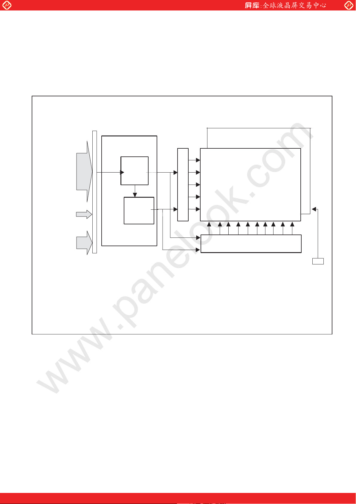
2.2 Functional Block Diagram
The following diagram shows the functional block of the 15.0 inches Color TFT/LCD
Module:
www.panelook.com
LCD DRIVE
CARD
6bit color
for R/G/B
DSPTMG
Vsync
Hsync
(3 pairs LVDS)
DTCLK
(1 pair LVDS)
VDD
GND
LCD
Controller
DC-DC
Converter
Ref circuit
LCD Connector
JAE JAE FI-XB30R-HF11
Mating Type JAE FI-S30M
TFT
Backlight Unit
1024(R/G/B) x 3
Y-Driver
X-Driver
JST BHSR-02VS-1
Mating T
Lamp Connector
2B-BHSS-1
(C) Copyright AU Optronics, Inc.
August, 2001 All Rights Reserved. B150XG01 V7 Ver.01
No Reproduction and Redistribution Allowed.
One step solution for LCD / PDP / OLED panel application: Datasheet, inventory and accessory!
6/19
www.panelook.com
Page 7

Global LCD Panel Exchange Center
3.0 Absolute Maximum Ratings
www.panelook.com
Absolute maximum ratings of the module is as following:
Item Symbol Min Max Unit Conditions
Logic/LCD Drive Voltage VDD -0.3 +4.0 [Volt]
Input Voltage of Signal Vin -0.3 VDD+0.3 [Volt]
CCFL Current ICFL - 7 [mA]
rms
CCFL Ignition Voltage Vs - 1150 Vrms
Operating Temperature TOP 0 +50 [oC] Note 1
Operating Humidity HOP 8 95 [%RH] Note 1
Storage Temperature TST -20 +60 [oC] Note 1
Storage Humidity HST 5 95 [%RH] Note 1
Vibration 1.5 10-500
G Hz 2hr/axis, X,Y,Z
(random)
Shock 220 , 2 G ms Half sine wave
Note 1 : Maximum Wet-Bulb should be 39к and No condensation.
(C) Copyright AU Optronics, Inc.
August, 2001 All Rights Reserved. B150XG01 V7 Ver.01
No Reproduction and Redistribution Allowed.
7/19
One step solution for LCD / PDP / OLED panel application: Datasheet, inventory and accessory!
www.panelook.com
Page 8

Global LCD Panel Exchange Center
www.panelook.com
4.0 Optical Characteristics
The optical characteristics are measured under stable conditions as follows under 25к
condition:
Item Conditions Typ. Note
Viewing Angle
K: Contrast Ratio
Contrast ratio
Luminance
[degree]
[degree]
[degree]
[degree]
Horizontal (Right)
K = 10 (Left)
Vertical (Upper)
K = 10 (Lower)
300 —
1.25 max. (5 pts)
Uniformity
Response Time [msec] Rising
(Room Temp.) [msec] Falling
Color Red x
Chromaticity Red
y 0.326+-0.03
Coordinates (CIE) Green x
Green
Blue x
y 0.542+-0.03
40
40
10
30
1.65 max. (13pts)
24 15(Max.)
11 30(Max.)
0.576+-0.03
0.315+-0.03
0.149+-0.03
——
—
—
White Luminance
[cd/m2]
Blue
White x
White
(CCFL 6.0 mA)
y 0.135+-0.03
0.313+-0.03
y 0.329+-0.03
180 (5 points average)
200 (center)
(C) Copyright AU Optronics, Inc.
August, 2001 All Rights Reserved. B150XG01 V7 Ver.01
No Reproduction and Redistribution Allowed.
8/19
One step solution for LCD / PDP / OLED panel application: Datasheet, inventory and accessory!
www.panelook.com
Page 9

Global LCD Panel Exchange Center
5.0 Signal Interface
5.1 Connectors
Physical interface is described as for the connector on module.
These connectors are capable of accommodating the following signals and will be following
components.
Connector Name / Designation For Signal Connector
Manufacturer JAE or compatible
Type / Part Number FI-XB30SR-HF11 or compatible
Mating Housing/Part Number FI-X30M, FI-X30C or FI-X30H
www.panelook.com
Mating Contact/Part Number FI-C3-A1
Connector Name / Designation For Lamp Connector
Manufacturer JST
Type / Part Number BHSR-02VS-1
Mating Type / Part Number SM02B-BHSS-1-TB
5.2 Signal Pin
Pin# Signal Name Pin# Signal Name
1 GND 2 VDD
3 VDD 4 VEDID
5 NC 6 CLKEDID
7 DATAEDID 8 RxIN0-
9 RxIN0+ 10 GND
11 RxlN1- 12 RxlN1+
13 GND 14 RxIN215 RxIN2+ 16 GND
17 RxCLKIN- 18 RxCLKIN+
19 GND 20 GND
21 NC 22 NC
23 NC 24 NC
25 NC 26 NC
27 NC 28 NC
29 NC 30 NC
(C) Copyright AU Optronics, Inc.
August, 2001 All Rights Reserved. B150XG01 V7 Ver.01
No Reproduction and Redistribution Allowed.
One step solution for LCD / PDP / OLED panel application: Datasheet, inventory and accessory!
9/19
www.panelook.com
Page 10

Global LCD Panel Exchange Center
5.3 Signal Description
The module using a LVDS receiver. LVDS is a differential signal technology for LCD interface
and high speed data transfer device. Transmitter shall be SN75LVDS84 (negative edge
sampling) or compatible.
Signal Name Description
RxIN0-, RxIN0+ LVDS differential data input(Red0-Red5, Green0)
RxIN1-, RxIN1+ LVDS differential data input(Green1-Green5, Blue0-Blue1)
RxIN2-, RxIN2+ LVDS differential data input(Blue2-Blue5, Hsync, Vsync, DSPTMG)
RxCLKIN-, RxCLKIN0+ LVDS differential clock input
www.panelook.com
VDD +3.3V Power Supply
GND Ground
Note: Input signals shall be low or Hi-Z state when VDD is off.
Internal circuit of LVDS inputs are as following.
(C) Copyright AU Optronics, Inc.
August, 2001 All Rights Reserved. B150XG01 V7 Ver.01
No Reproduction and Redistribution Allowed.
One step solution for LCD / PDP / OLED panel application: Datasheet, inventory and accessory!
10/19
www.panelook.com
Page 11

Global LCD Panel Exchange Center
Signal Input
Pin No.
8
RxIN0-
www.panelook.com
SN75LVDS86 or Compatible
R
9
11
12
14
15
17
18
RxIN0+
RxIN1-
RxIN1+
RxIN2-
RxIN2+
RxCLKIN-
RxCLKIN+
R
R
R
The module uses a 100ohm resistor between positive and negative data lines of
each receiver input
Signal Name Description
RED5
RED4
RED3
RED2
RED1
RED0
Red Data 5 (MSB)
Red Data 4
Red Data 3
Red Data 2
Red Data 1
Red Data 0 (LSB)
Red-pixel Data
Each red pixel's brightness data consists of
these 6 bits pixel data.
Red-pixel Data
(C) Copyright AU Optronics, Inc.
August, 2001 All Rights Reserved. B150XG01 V7 Ver.01
No Reproduction and Redistribution Allowed.
11/19
One step solution for LCD / PDP / OLED panel application: Datasheet, inventory and accessory!
www.panelook.com
Page 12

Global LCD Panel Exchange Center
www.panelook.com
GREEN 5
GREEN 4
GREEN 3
GREEN 2
GREEN 1
GREEN 0
Green Data 5 (MSB)
Green Data 4
Green Data 3
Green Data 2
Green Data 1
Green Data 0 (LSB)
Green-pixel Data
Each green pixel's brightness data consists of
these 6 bits pixel data.
Green-pixel Data
BLUE 5
BLUE 4
BLUE 3
BLUE 2
BLUE 1
BLUE 0
Blue Data 5 (MSB)
Blue Data 4
Blue Data 3
Blue Data 2
Blue Data 1
Blue Data 0 (LSB)
Blue-pixel Data
Each blue pixel's brightness data consists of
these 6 bits pixel data.
Blue-pixel Data
DTCLK Data Clock The typical frequency is 54.0 MHZ.. The signal
is used to strobe the pixel data and DSPTMG
signals. All pixel data shall be valid at the falling
edge when the DSPTMG signal is high.
DSPTMG Display Timing This signal is strobed at the falling edge of
-DTCLK. When the signal is high, the pixel data
shall be valid to be displayed.
VSYNC Vertical Sync The signal is synchronized to -DTCLK .
HSYNC Horizontal Sync The signal is synchronized to -DTCLK .
Note: Output signals from any system shall be low or Hi-Z state when VDD is off.
5.4 Signal Electrical Characteristics
Input signals shall be low or Hi-Z state when VDD is off.
It is recommended to refer the specifications of SN75LVDS86DGG(Texas Instruments) in
detail.
Signal electrical characteristics are as follows;
Parameter Condition Min Max Unit
Vth
Vtl
Differential Input High
Voltage(Vcm=+1.2V)
Differential Input Low
Voltage(Vcm=+1.2V)
(C) Copyright AU Optronics, Inc.
August, 2001 All Rights Reserved. B150XG01 V7 Ver.01
No Reproduction and Redistribution Allowed.
-100
100
[mV]
[mV]
12/19
One step solution for LCD / PDP / OLED panel application: Datasheet, inventory and accessory!
www.panelook.com
Page 13

Global LCD Panel Exchange Center
g
p
p
LVDS Macro AC characteristics are as follows:
Min. Max.
Clock Frequency (T) 50MHZ 68MHZ
Data Setup Time (Tsu) 600ps
Data Hold Time (Thd) 600ps
Input Clock
www.panelook.com
T
Input Data
5.5 Signal for Lamp connector
Pin #
1
2
Si
Lam
Lam
nal Name
High Voltage
Low Voltage
ThdTsu
(C) Copyright AU Optronics, Inc.
August, 2001 All Rights Reserved. B150XG01 V7 Ver.01
No Reproduction and Redistribution Allowed.
One step solution for LCD / PDP / OLED panel application: Datasheet, inventory and accessory!
13/19
www.panelook.com
Page 14

Global LCD Panel Exchange Center
www.panelook.com
6.0 Pixel Format Image
Following figure shows the relationship of the input signals and LCD pixel format.
VW/LQH
WK/LQH
5 * % 5 * %
5 * % 5 * %
7.0 Parameter guide line for CFL Inverter
Parameter Min DP-1 Max Units Condition
5 * % 5 * %
5 * % 5 * %
White Luminance
5 points average
-
180
⎯
[cd/m
CCFL current(ICFL) 3.0 6.0 7.0 [mA]
rms
CCFL Frequency(FCFL) 40 50 60 [KHz]
2
]
(Ta=25к)
(Ta=25к)
Note 2
(Ta=25к)
Note 3
CCFL Ignition Voltage(Vs)
CCFL Voltage (Reference)
⎯
(VCFL)
CCFL Power consumption
⎯
(PCFL)
⎯
700
4.2
1,150
⎯
⎯
[Volt]
rms
[Volt]
rms
[Watt]
(Ta= 0к)
Note 4
(Ta=25к)
Note 5
(Ta=25к)
Note 5
Note 1: DP-1 are AUO recommended Design Points.
*1 All of characteristics listed are measured under the condition using the AUO Test inverter.
(C) Copyright AU Optronics, Inc.
August, 2001 All Rights Reserved. B150XG01 V7 Ver.01
No Reproduction and Redistribution Allowed.
14/19
One step solution for LCD / PDP / OLED panel application: Datasheet, inventory and accessory!
www.panelook.com
Page 15

Global LCD Panel Exchange Center
www.panelook.com
*2 In case of using an inverter other than listed, it is recommended to check the inverter
carefully. Sometimes, interfering noise stripes appear on the screen, and substandard
luminance or flicker at low power may happen.
*3 In designing an inverter, it is suggested to check safety circuit ver carefully. Impedance of
CFL, for instance, becomes more than 1 [M ohm] when CFL is damaged.
*4 Generally, CFL has some amount of delay time after applying kick-off voltage. It is
recommended to keep on applying kick-off voltage for 1 [Sec] until discharge.
*5 CFL discharge frequency must be carefully chosen so as not to produce interfering noise
stripes on the screen.
*6 Reducing CFL current increases CFL discharge voltage and generally increases CFL
discharge frequency. So all the parameters of an inverter should be carefully designed so as
not to produce too much leakage current from high-voltage output of the inverter.
Note 2: It should be emplyed the inverter which has “Duty Dimming”, if ICFL is less than 4mA.
Note 3: CFL discharge frequency should
be carefully determined to avoid interference between inverter and TFT LCD.
Note 4: CFL inverter should be able to give out a power that has a generating capacity of over
1,400 voltage. Lamp units need 1,400 voltage minimum for ignition.
Note 5: Calculator value for reference (ICFL×VCFL=PCFL)
8.0 Interface Timings
Basically, interface timings should match the VESA 1024x768 /60Hz (VG901101) manufacturing
guide line timing.
8.1 Timing Characteristics
Symbol Description Min Typ Max Unit
fdck DTCLK Frequency
tck DTCLK cycle time
tx X total time 1206 1344 1648 [tck]
tacx X active time
tbkx X blank time 90 320
Hsync H frequency
Hsw H-Sync width 2 136
Hbp H back porch 4 160
Hfp H front porch 8 24
ty Y total time 771 806 895 [tx]
tacy Y active time
Vsync Frame rate (55) 60 61 [Hz]
Vw V-sync Width 2 6
Vfp V-sync front porch 1 3
Vbp V-sync back porch 7 29 63 [tx]
50
Note: Hsw(H-sync width) + Hbp(H-sync back porch) should be less than 515 tck.
65.00
15.38
1024
48.363
768
68
[MHz]
[nsec]
[tck]
[tck]
[KHz]
[tck]
[tck]
[tck]
[tx]
[tx]
[tx]
(C) Copyright AU Optronics, Inc.
August, 2001 All Rights Reserved. B150XG01 V7 Ver.01
No Reproduction and Redistribution Allowed.
One step solution for LCD / PDP / OLED panel application: Datasheet, inventory and accessory!
15/19
www.panelook.com
Page 16

Global LCD Panel Exchange Center
t
S
9t
6t
S
8.2 Timing Definition
www.panelook.com
x
H-Sync
HbpHfp
Hsw
PTM
D
V-Sync
3tx
2
x
PTM
D
38tx
9.0 Power Consumption
tacx
x
768tx
Input power specifications are as follows;
Symble Parameter Min Typ Max Units Condition
VDD Logic/LCD Drive
3.0 3.3 3.6 [Volt] Load Capacitance 20uF
Voltage
PDD VDD Power
PDD Max VDD Power max
IDD IDD Current
IDD Max IDD Current max
VDDrp Allowable
Logic/LCD Drive
1.26 [Watt] All Black Pattern
380
1.91 [Watt] Max Pattern Note
mA
580 mA
100 [mV]
All Black Pattern
Max Pattern Note
p-p
Ripple Voltage
VDDns Allowable
Logic/LCD Drive
100 [mV]
p-p
Ripple Noise
Note : VDD=3.3V
(C) Copyright AU Optronics, Inc.
August, 2001 All Rights Reserved. B150XG01 V7 Ver.01
No Reproduction and Redistribution Allowed.
16/19
One step solution for LCD / PDP / OLED panel application: Datasheet, inventory and accessory!
www.panelook.com
Page 17

Global LCD Panel Exchange Center
n
www.panelook.com
10. Power ON/OFF Sequence
VDD power and lamp on/off sequence is as follows. Interface signals are also shown in
the chart. Signals from any system shall be Hi-Z state or low level when VDD is off.
90%
VDD
0 V
Signals
Lamp O
0 V
0 V
10%
10ms max.
0-50 ms
10%
0-50 ms
10%
200ms min.
200ms min
10%
10%
90%
400ms min.
10%
10%
(C) Copyright AU Optronics, Inc.
August, 2001 All Rights Reserved. B150XG01 V7 Ver.01
No Reproduction and Redistribution Allowed.
One step solution for LCD / PDP / OLED panel application: Datasheet, inventory and accessory!
17/19
www.panelook.com
Page 18

Global LCD Panel Exchange Center
11. Mechanical Characteristics
www.panelook.com
(C) Copyright AU Optronics, Inc.
August, 2001 All Rights Reserved. B150XG01 V7 Ver.01
No Reproduction and Redistribution Allowed.
18/19
One step solution for LCD / PDP / OLED panel application: Datasheet, inventory and accessory!
www.panelook.com
Page 19

Global LCD Panel Exchange Center
www.panelook.com
(C) Copyright AU Optronics, Inc.
August, 2001 All Rights Reserved. B150XG01 V7 Ver.01
No Reproduction and Redistribution Allowed.
One step solution for LCD / PDP / OLED panel application: Datasheet, inventory and accessory!
19/19
www.panelook.com
 Loading...