

Global LCD Panel Exchange Center
www.panelook.com
Product Specification
AU OPTRONICS CORPORATION
( ) Preliminary Specifications
(V ) Final Specifications
Module 14.1” WXGA Color TFT-LCD with LED Backlight design
Model Name
Note ( )
B141EW05 V5 (Dell P/N: 2H7P2)
LED Backlight with driving circuit design
Customer Date
Checked &
Date
Approved by
Approved by Date
Bonnie Chen 02/12/2010
Prepared by
Note: This Specification is subject to change
without notice.
B141EW05 V5 Document Version : 1.0
One step solution for LCD / PDP / OLED panel application: Datasheet, inventory and accessory!
Kay CY Wang 02/12/2010
NBBU Marketing Division /
AU Optronics corporation
1 of 34
www.panelook.com

Global LCD Panel Exchange Center
www.panelook.com
Product Specification
AU OPTRONICS CORPORATION
Contents
1. Handling Precautions .............................................................. 4
2. General Description ................................................................. 5
2.1 General Specification ...............................................................................................................................5
2.2 Optical Characteristics .............................................................................................................................6
3. Functional Block Diagram ...................................................... 11
4. Absolute Maximum Ratings ................................................... 12
4.1 Absolute Ratings of TFT LCD Module............................................................................................... 12
4.2 Absolute Ratings of Environment ........................................................................................................ 12
5. Electrical characteristics ....................................................... 13
5.1 TFT LCD Module ................................................................................................................................. 13
5.2 Backlight Unit........................................................................................................................................ 16
6. Signal Characteristic ............................................................. 17
6.1 Pixel Format Image................................................................................................................................ 17
6.2 The input data format ............................................................................................................................ 18
6.3 Integration Interface and Pin Assignment............................................................................................ 19
6.4 Interface Timing..................................................................................................................................... 21
7. Vibration and Shock Test ....................................................... 24
7.1 Vibration Test......................................................................................................................................... 24
7.2 Shock Test Spec:.................................................................................................................................... 24
7.3 Reliability Test .................................................................... 25
8. Mechanical Characteristics .................................................... 26
8.1 LCM Outline Dimension ...................................................................................................................... 26
8.2 Screw Hole Depth and Center Position ............................................................................................... 28
9. Shipping and Package............................................................ 29
9.1 Shipping Label Format ......................................................................................................................... 29
9.2 Carton package ...................................................................................................................................... 30
9.3 Shipping package of palletizing sequence .......................................................................................... 30
10. Appendix: EDID description ................................................. 31
B141EW05 V5 Document Version : 1.0
One step solution for LCD / PDP / OLED panel application: Datasheet, inventory and accessory!
2 of 34
www.panelook.com
Global LCD Panel Exchange Center
www.panelook.com
Product Specification
AU OPTRONICS CORPORATION
Record of Revision
Version and Date Page Old description New Description Remark
0.1 2009/07/14 All First Edition for Customer
0.2 2010/01/29 P. 6 TBD Update Chromaticity Coodinates
1.0 2010/02/12 P.27-28
P.32-35
1.1 2010/11/22 P.29 Shipping label New shipping label for Pol 25%
Old 2D drawing
X31 EDID
New 2D drawing w/ W WAN solution
A00 EDID
B141EW05 V5 Document Version : 1.0
One step solution for LCD / PDP / OLED panel application: Datasheet, inventory and accessory!
3 of 34
www.panelook.com

Global LCD Panel Exchange Center
www.panelook.com
Product Specification
AU OPTRONICS CORPORATION
1. Handling Precautions
1) Since front polarizer is easily damaged, pay attention not to scratch it.
2) Be sure to turn off power supply when inserting or disconnecting from input connector.
3) Wipe off water drop immediately. Long contact with water may cause discoloration or
spots.
4) When the panel surface is soiled, wipe it with absorbent cotton or other soft cloth.
5) Since the panel is made of glass, it may break or crack if dropped or bumped on hard
surface.
6) Since CMOS LSI is used in this module, take care of static electricity and insure
human earth when handling.
7) Do not open nor modify the Module Assembly.
8) Do not press the reflector sheet at the back of the module to any directions.
9) At the insertion or removal of the Signal Interface Connector, be sure not to rotate nor
tilt the Interface Connector of the TFT Module.
11) After installation of the TFT Module into an enclosure (Notebook PC Bezel, for
example), do not twist nor bend the TFT Module even momentary. At designing the
enclosure, it should be taken into consideration that no bending/twisting forces are
applied to the TFT Module from outside. Otherwise the TFT Module may be
damaged.
12) Small amount of materials having no flammability grade is used in the LCD module. The LCD
module should be supplied by power complied with requirements of Limited Power Source
(IEC60950 or UL1950), or be applied exemption.
13) Disconnecting power supply before handling LCD modules, it can prevent electric shock, DO
NOT TOUCH the electrode parts, cables, connectors and LED circuit part of TFT module
that a LED light bar build in as a light source of back light unit. High voltage is supplied to
these parts when power turn on.
B141EW05 V5 Document Version : 1.0
One step solution for LCD / PDP / OLED panel application: Datasheet, inventory and accessory!
4 of 34
www.panelook.com
Global LCD Panel Exchange Center
www.panelook.com
Product Specification
AU OPTRONICS CORPORATION
2. General Description
B141EW05 V5 is a Color Active Matrix Liquid Crystal Display composed of a TFT LCD panel, a
driver circuit, and LED backlight system. The screen format is intended to support the WXGA
(1280(H) x 800(V)) screen and 262k colors (RGB 6-bits data driver) with LED backlight driving
circuit. The input signals are eDP interface compatible.
B141EW05 V5 is designed for a display unit of notebook style personal computer and industrial
machine.
2.1 General Specification
The following items are characteristics summary on the table at 25 ʚ condition:
Items Unit Specifications
Screen Diagonal [mm] 357.7 (14.1W”)
Active Area [mm] 303.36 X 189.6
Pixels H x V 1280x3(RGB) x 800
Pixel Pitch [mm] 0.237
Pixel Format R.G.B. Vertical Stripe
Display Mode Normally White
White Luminance (I
Note: I
LED
is LED current
LED
=20mA)
[cd/m
2
] 220 typ. (5 points average)
200 min. (5 points average)
Luminance Uniformity 1.25 max. (5 points)
Contrast Ratio 500:1 typ
Response Time [ms] 8 typ / 16 Max
Nominal Input Voltage VDD [Volt] +3.3 typ.
Power Consumption [Watt] 5.1 max. (Include Logic and Blu power)
(Note1)
Weight [Grams] 375 max.
Physical Size without inverter,
bracket.
[mm]
Min. Typ. Max.
Length 319 319.5 320
Width 206 206.5 207
Thickness - - 5.5
Electrical Interface 1 channel Display Port
Surface Treatment Anti-Glare,
B141EW05 V5 Document Version : 1.0
One step solution for LCD / PDP / OLED panel application: Datasheet, inventory and accessory!
5 of 34
www.panelook.com
Global LCD Panel Exchange Center
ge (
g)
[
]
www.panelook.com
Product Specification
AU OPTRONICS CORPORATION
Support Color 262K colors ( RGB 6-bit )
Temperature Range
Operating
Stora
Non-Operatin
RoHS Compliance RoHS Compliance
Note 1. T otal power consumption including LED power efficiency <4.9W max.
2.2 Optical Characteristics
The optical characteristics are measured under stable conditions at 25ʚ (Room Temperature) :
Item Symbol Conditions Min. Typ. Max. Unit Note
o
[
C]
o
C
0 to +50
-20 to +65
White Luminance
LED
=20mA
I
Viewing Angle
Luminance
Uniformity
Luminance
Uniformity
Contrast Ratio CR
Cross talk %
Response Time
Red x
Red y
Green x
Color /
Chromaticity
Coodinates
Green y
Blue x
Blue y
White x
White y
5 points average
R
L
H
L
5P
13P
Horizontal (Right)
CR = 10 (Left)
Vertical (Upper)
CR = 10 (Lower)
5 Points
13 Points
400 500 -
4
Tr Rising
Tf Falling
T
Rising + Falling
RT
CIE 1931!!!!
200 220 - cd/m
40
40
15
30
45
45
20
40
-
degree
-
-
-
- - 1.25
- - 1.50
-
- 2 -
6
-
msec
- 8 16
0.570 0.600 0.630
0.310 0.340 0.370
0.285 0.315 0.345
0.520 0.550 0.580
0.125 0.155 0.185
0.115 0.145 0.175
0.283 0.313 0.343
0.299 0.329 0.359
2
1, 4, 5.
4, 9
1, 3, 4
2, 3, 4
4, 6
4, 7
4, 8
4
NTSC %
B141EW05 V5 Document Version : 1.0
One step solution for LCD / PDP / OLED panel application: Datasheet, inventory and accessory!
- 45 -
6 of 34
www.panelook.com
Global LCD Panel Exchange Center
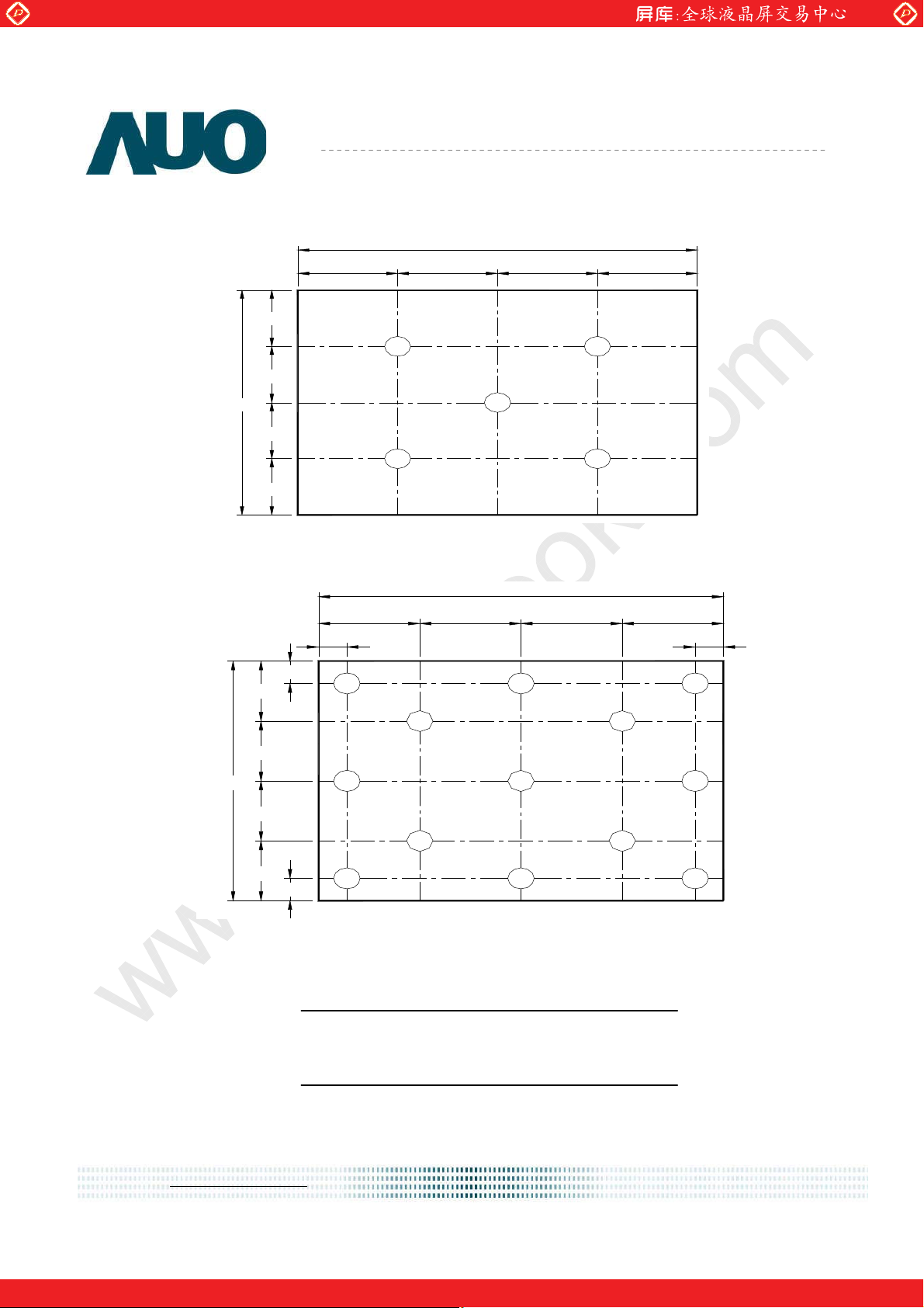
Note 1: 5 points position (Ref: Active area)
H/4
H/4
www.panelook.com
Product Specification
AU OPTRONICS CORPORATION
W
W/4 W/4 W/4 W/4
12
H
H/4
H/4
Note 2: 13 points position (Ref: Active area)
W/4
10
10
H/4
H/4
H
H/4
1
6
3
45
W
W/4
W/4
2
W/4
10
3
45
7
9
10
8
H/4
10
11
12
13
Note 3: The luminance uniformity of 5 or13 points is defined by dividing the maximum luminance values by the
minimum test point luminance
Maximum Brightness of five points
Ӭ
=
W5
Minimum Brightness of five points
Maximum Brightness of thirteen points
W13
=
Minimum Brightness of thirteen points
Ӭ
Note 4: Measurement method
B141EW05 V5 Document Version : 1.0
One step solution for LCD / PDP / OLED panel application: Datasheet, inventory and accessory!
7 of 34
www.panelook.com
Global LCD Panel Exchange Center
g
g
www.panelook.com
Product Specification
AU OPTRONICS CORPORATION
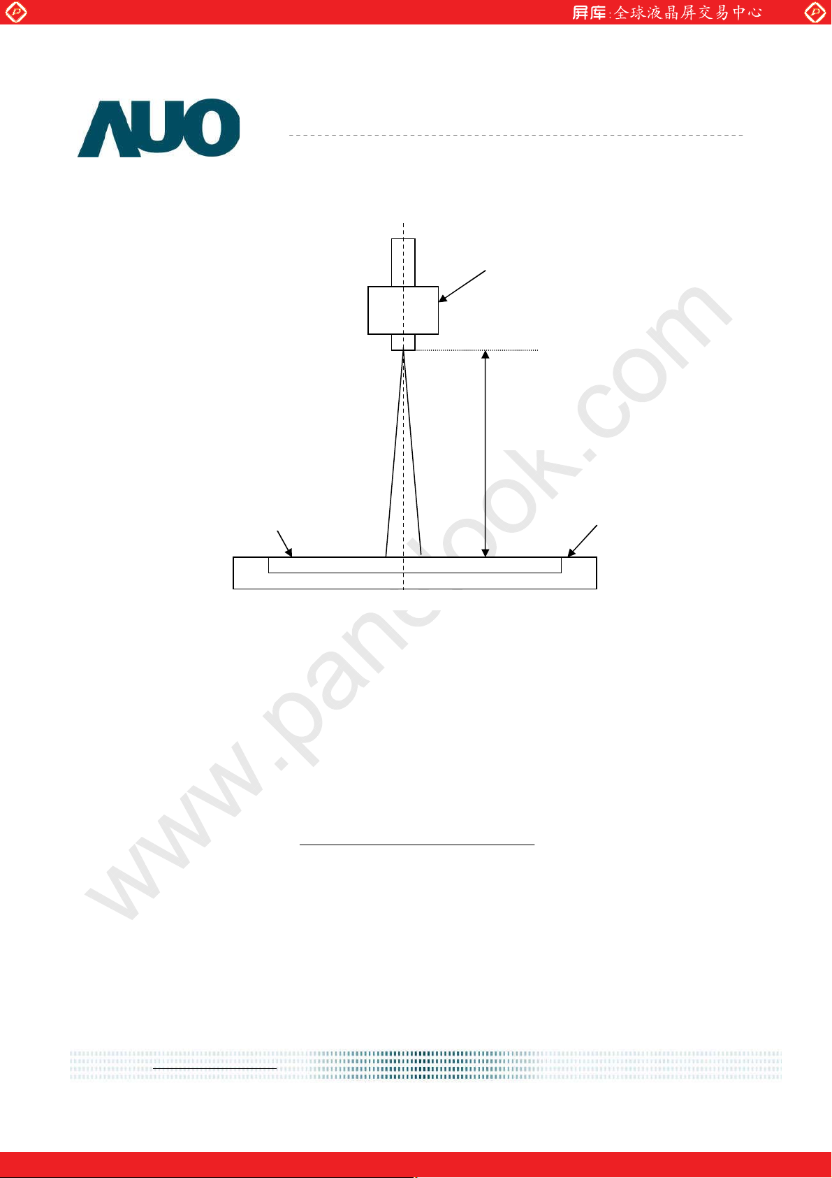
The LCD module should be stabilized at given temperature for 30 minutes to avoid abrupt temperature change
during measuring. In order to stabilize the luminance, the measurement should be executed after lighting
Backlight for 30 minutes in a stable, windless and dark room, , and it should be measured in the center of screen.!!
Photo detector
Field=2
Note 5Ǻ Definition of Average Luminance of White (Y
Measure the luminance of gray level 63 at 5 pointsǴY
L (x) is corresponding to the luminance of the point X at Figure in Note (1).
Note 6Ǻ Definition of contrast ratio:
Contrast ratio is calculated with the following formula.
htness on the “White” state
Bri
):
L
= [L (1)+ L (2)+ L (3)+ L (4)+ L (5)] / 5
L
Contrast ratio (CR)=
htness on the “Black” state
Bri
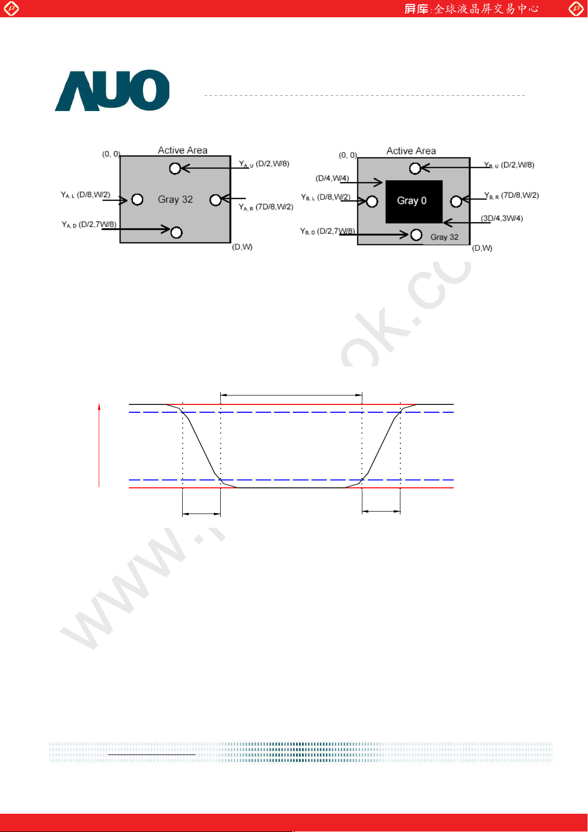
Note 7Ǻ Definition of Cross Talk (CT)
-
B
CT = | Y
Where
A
Y
B141EW05 V5 Document Version : 1.0
One step solution for LCD / PDP / OLED panel application: Datasheet, inventory and accessory!
– YA | / YA × 100 (%)
= Luminance of measured location without gray level 0 pattern (cd/m2)
8 of 34
www.panelook.com
Global LCD Panel Exchange Center
YB = Luminance of measured location with gray level 0 pattern (cd/m2)
Note 8: Definition of response time:
www.panelook.com
Product Specification
AU OPTRONICS CORPORATION
The output signals of BM-7 or equivalent are measured when the input signals are changed from “Black” to
“White” (falling time) and from “White” to “Black” (rising time), respectively. The response time interval between the
10% and 90% of amplitudes. Refer to figure as below.
"Black"
100%
S
ig
90%
n
a
l(
R
e
la
t
iv
e
v
a
lu
10%
e
)
0%
Tr
Tf
"White""White"
B141EW05 V5 Document Version : 1.0
One step solution for LCD / PDP / OLED panel application: Datasheet, inventory and accessory!
9 of 34
www.panelook.com
Global LCD Panel Exchange Center
www.panelook.com
Product Specification
AU OPTRONICS CORPORATION
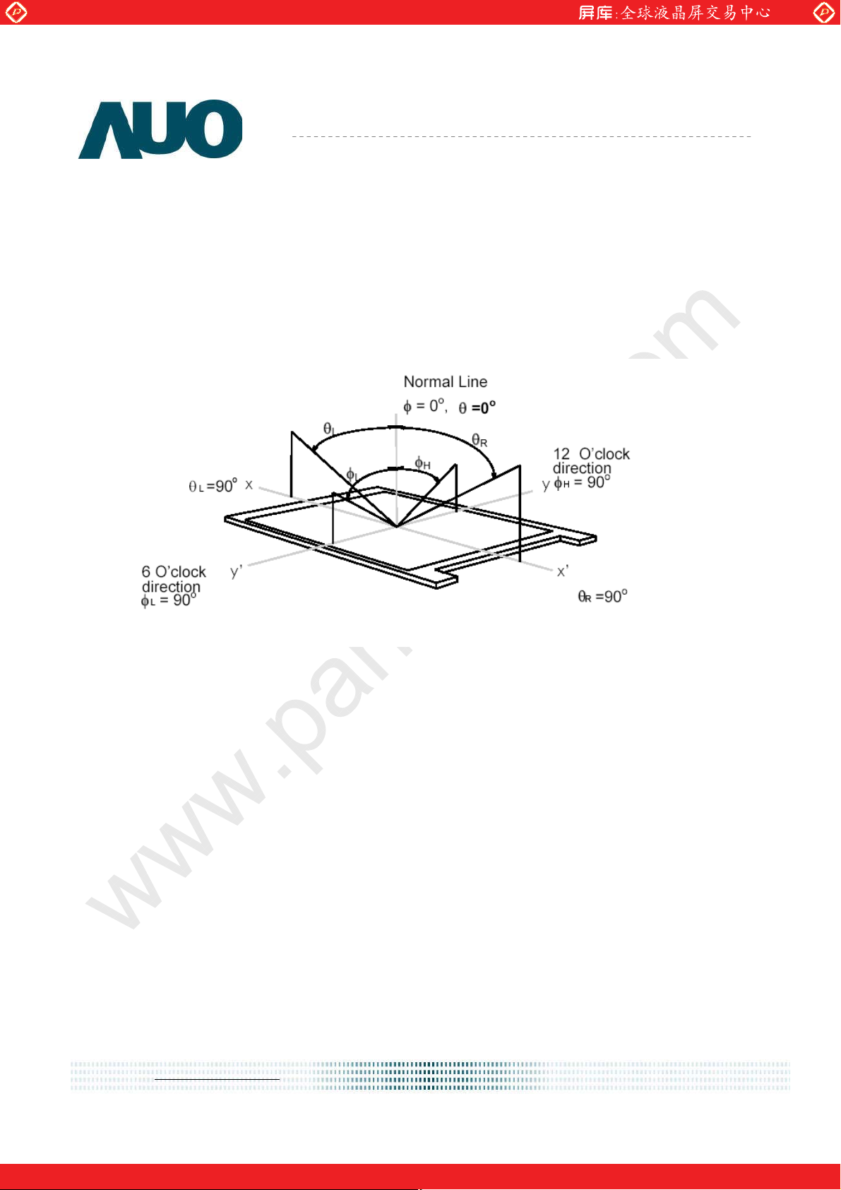
Note 9. Definition of viewing angle
Viewing angle is the measurement of contrast ratio ɪ10, at the screen center, over a 180° horizontal an d 180°
vertical range (off-normal viewing angles). The 180° viewing angle range is broken down as follows; 90 ° ( θ)
horizontal left and right and 90° ( Φ) vertical, high (up) and low (down). The measurement direction is typically
perpendicular to the display surface with the screen rotated about its center to develop the desired measurement
viewing angle.
B141EW05 V5 Document Version : 1.0
One step solution for LCD / PDP / OLED panel application: Datasheet, inventory and accessory!
10 of 34
www.panelook.com

Global LCD Panel Exchange Center
www.panelook.com
Product Specification
AU OPTRONICS CORPORATION
3. Functional Block Diagram
The following diagram shows the functional block of the 14.1 inches wide Color TFT/LCD 30 Pin (One
ch/connector Module:
B141EW05 V5 Document Version : 1.0
One step solution for LCD / PDP / OLED panel application: Datasheet, inventory and accessory!
11 of 34
www.panelook.com

Global LCD Panel Exchange Center
Product Specification
AU OPTRONICS CORPORATION
4. Absolute Maximum Ratings
An absolute maximum rating of the module is as following:
4.1 Absolute Ratings of TFT LCD Module
Item Symbol Min Max Unit Conditions
Logic/LCD Drive
4.2 Absolute Ratings of Environment
Item Symbol Min Max Unit Conditions
Operating
Operation Humidity HOP 8 95 [%RH] Note 4
Storage Temperature TST -20 +65 [oC] Note 4
Storage Humidity HST
Vin -0.3 +4.0 [Volt] Note 1,2
TOP 0 +50 [
www.panelook.com
5 95
o
C] Note 4
[%RH]
Note 4
Note 1: At Ta (25ʚ )
Note 2: Permanent damage to the device may occur if exceed maximum values
Note 3: LED specification refer to section 5.2
Note 4: For quality performance, please refer to AUO IIS (Incoming Inspection Standard).
Twb=39°C
Operating Range
B141EW05 V5 Document Version : 1.0
Storage Range
One step solution for LCD / PDP / OLED panel application: Datasheet, inventory and accessory!
12 of 34
www.panelook.com

Global LCD Panel Exchange Center
g
www.panelook.com
Product Specification
AU OPTRONICS CORPORATION
5. Electrical characteristics
5.1 TFT LCD Module
5.1.1 Power Specification
Input power specifications are as follows;
The power specification are measured under 25ʚ and frame frenquency under 60Hz
Symble Parameter Min Typ Max Units Note
VDD Logic/LCD Drive
Volta
e
PDD VDD Power
IDD IDD Current
I
Rush
Inrush Current
VDDrp Allowable
Logic/LCD Drive
Ripple Voltage
3.0 3.3 3.6 [Volt]
-
- -
- -
- -
- 1.6 [Watt] Note 1/2
450
[mA]
2000 [mA]
100 [mV]
p-p
Note 1/2
Note 3
Note 1 : Maximum Measurement ConditionǺBlack Pattern
Note 2ǺTypical Measurement Condition: Mosaic Pattern
Note 3ǺMeasure Condition
90%
3.3V
10%
0V
0.5ms
B141EW05 V5 Document Version : 1.0
One step solution for LCD / PDP / OLED panel application: Datasheet, inventory and accessory!
Vin rising time
13 of 34
www.panelook.com

Global LCD Panel Exchange Center
5.1.2 Signal Electrical Characteristics
Input signals shall be low or High-impedance state when VDD is off.
It is recommended to refer the specifications of VESA Display Port Standard V1.1a (Thine
Electronics Inc.) in detail.
Signal electrical characteristics are as follows;
Display Port main link signal:
www.panelook.com
Product Specification
AU OPTRONICS CORPORATION
Fallow as VESA display port standard V1.1a at both 1.62 and 2.7Gbps link rates.
B141EW05 V5 Document Version : 1.0
One step solution for LCD / PDP / OLED panel application: Datasheet, inventory and accessory!
14 of 34
www.panelook.com

Global LCD Panel Exchange Center
Display Port AUX_CH signal:
www.panelook.com
Product Specification
AU OPTRONICS CORPORATION
Fallow as VESA display port standard V1.1a.
Display Port V
Fallow as VESA display port standard V1.1a.
HPD
signal:
B141EW05 V5 Document Version : 1.0
One step solution for LCD / PDP / OLED panel application: Datasheet, inventory and accessory!
15 of 34
www.panelook.com

Global LCD Panel Exchange Center
5.2 Backlight Unit
5.2.1 LED characteristics
www.panelook.com
Product Specification
AU OPTRONICS CORPORATION
Parameter
Backlight Power
Consumption
LED Life-Time
Note 1: Calculator value for reference P
Note 2: The LED life-time define as the estimated time to 50% degradation of initial luminous.
Symbol
Min Typ Max Units Condition
PLED - - 3.5
N/A 10,000 - -
= VF (Normal Distribution) * IF (Normal Distribution) / Efficiency
LED
[Watt]
Hour
(Ta=25ʚ), Note 1
Vin =12V
(Ta=25ʚ), Note 2
I
F
5.2.2 Backlight input signal characteristics
Parameter
Symbol
Min Typ Max Units Remark
LED Power Supply VLED 7.5 12.0 21.0 [Volt]
LED Enable Input
3.0 - 5.5 [Volt]
High Level
LED Enable Input
VLED_EN
- - 0.8 [Volt]
Low Level
PWM Logic Input
High Level
PWM Logic Input
2.5 - 5.5
VPWM_EN
- - 0.8
[Volt]
[Volt]
Low Level
=20 mA
Define as
Connector
Interface
(Ta=25ʚ)
PWM Input Frequency
PWM Duty Ratio
B141EW05 V5 Document Version : 1.0
One step solution for LCD / PDP / OLED panel application: Datasheet, inventory and accessory!
FPWM 9.5 10 10.5
Duty 5 -- 100
KHz
%
16 of 34
www.panelook.com

Global LCD Panel Exchange Center
www.panelook.com
Product Specification
AU OPTRONICS CORPORATION
6. Signal Characteristic
6.1 Pixel Format Image
Following figure shows the relationship of the input signals and LCD pixel format.
1 1280
1st Line
800th Line
R G B B G R
R G B
R
G B
R G B R G B
R G B R G
B
B141EW05 V5 Document Version: 0.1
One step solution for LCD / PDP / OLED panel application: Datasheet, inventory and accessory!
17 of 34
www.panelook.com

Global LCD Panel Exchange Center
www.panelook.com
Product Specification
AU OPTRONICS CORPORATION
6.2 The input data format
Signal Name Description
R5
R4
R3
R2
R1
R0
Red Data 5 (MSB)
Red Data 4
Red Data 3
Red Data 2
Red Data 1
Red Data 0 (LSB)
Red-pixel Data
Each red pixel's brightness data consists of
these 6 bits pixel data.
Red-pixel Data
G5
G4
G3
G2
G1
G0
Green Data 5 (MSB)
Green Data 4
Green Data 3
Green Data 2
Green Data 1
Green Data 0 (LSB)
Green-pixel Data
Each green pixel's brightness data consists of
these 6 bits pixel data.
Green-pixel Data
B5
B4
B3
B2
B1
B0
Blue Data 5 (MSB)
Blue Data 4
Blue Data 3
Blue Data 2
Blue Data 1
Blue Data 0 (LSB)
Blue-pixel Data
Each blue pixel's brightness data consists of
these 6 bits pixel data.
Blue-pixel Data
RxCLKIN Data Clock The signal is used to strobe the pixel data and
DE signals. All pixel data shall be valid at the
falling edge when the DE signal is high.
DE Display Timing This signal is strobed at the falling edge of
RxCLKIN. When the signal is high, the pixel
data shall be valid to be displayed.
VS Vertical Sync The signal is synchronized to RxCLKIN .
HS Horizontal Sync The signal is synchronized to RxCLKIN .
Note: Output signals from any system shall be low or High-impedance state when VDD is off.
B141EW05 V5 Document Version: 0.1
One step solution for LCD / PDP / OLED panel application: Datasheet, inventory and accessory!
18 of 34
www.panelook.com

Global LCD Panel Exchange Center
www.panelook.com
Product Specification
AU OPTRONICS CORPORATION
6.3 Integration Interface and Pin Assignment
6.3.1 Connector Description
Physical interface is described as for the connector on module.
These connectors are capable of accommodating the following signals and will be following
components.
Connector Name / Designation For Signal Connector
Manufacturer IPEX or compatible
Type / Part Number
Mating Housing/Part Number
6.3.2 Pin Assignment
Pin # Signal Name Signal Descr. Pin # Signal Name Signal Descr.
1 PAID Conn. Continuity Test 16 LCD_GND LCD logic and driver ground
2 H_GND High Speed Ground 17 HPD HPD signal pin
3 Lane1_N Comp Signal Link Lane 1 18 BL_GND Backlight ground
4 Lane1_P True Signal Link Lane 1 19 BL_GND Backlight ground
5 H_GND High Speed Ground 20 BL_GND Backlight ground
6 Lane0_N Comp Signal Lane 0 21 BL_GND Backlight ground
7 Lane0_P True Signal Link Lane 0 22 NC No Connect
8 H_GND High Speed Ground 23 BL_PWM_DIM System PWM signal input
9 AUX_CH_P True Signal Auxiliary Ch. 24 SMBUS_CLK Backlight Control Clk
IPEX 20455-030E-12
IPEX 20453-030T-02
or compatible
or compatible
10 AUX_CH_N Comp Signal Auxiliary Ch. 25 SMBUS_DATA Backlight Control Data
11 H_GND High Speed Ground 26 BL_PWR Backlight power
12 LCD_VCC LCD logic and driver power 27 BL_PWR Backlight power
13 LCD_VCC LCD logic and driver power 28 BL_PWR Backlight power
14 BIST LCD Panel Self Test Enable 29 BL_PWR Backlight power
15 LCD_GND LCD logic and driver ground 30 PAID Conn. Continuity Test
B141EW05 V5 Document Version: 0.1
One step solution for LCD / PDP / OLED panel application: Datasheet, inventory and accessory!
19 of 34
www.panelook.com

Global LCD Panel Exchange Center
www.panelook.com
Product Specification
AU OPTRONICS CORPORATION
Note1: Start from right side
(Need to update to new drawing and connector location!!!!)
Note2: Input signals shall be low or High-impedance state when VDD is off.
B141EW05 V5 Document Version: 0.1
One step solution for LCD / PDP / OLED panel application: Datasheet, inventory and accessory!
20 of 34
www.panelook.com

Global LCD Panel Exchange Center
www.panelook.com
Product Specification
AU OPTRONICS CORPORATION
6.5 Power ON/OFF Sequence
VDD power on/off sequence is as follows. Interface signals are also shown in the chart. Signals
from any system shall be Hi-Z state or low level when VDD is off
Display Port panel power sequence:
Display Port AUX_CH transaction only:
B141EW05 V5 Document Version: 0.1
One step solution for LCD / PDP / OLED panel application: Datasheet, inventory and accessory!
21 of 34
www.panelook.com

Global LCD Panel Exchange Center
www.panelook.com
Product Specification
AU OPTRONICS CORPORATION
Display Port panel power sequence timing parameter:
Note 1: The sink must include the ability to generate black video autonomously. The sink must automatically enable
black video under the following conditions:
-upon LCDVDD power on (with in T2 max)
-when the "Novideostream_Flag" (VB-ID Bit 3) is received from the source (at the end of T9).
-when no main link data, or invalid video data, is received from the source. Black video must be displayed within
64ms (typ) from the start of either condition. Video data can be deemed invalid based on MSA and timing information,
for example.
Note 2: The sink may implement the ability to disable the black video function, as described in Note 1, above, for
system development and debugging purpose.
Note 3: The sink must support AUX_CH polling by the source immediately following LCDVDD power on without
B141EW05 V5 Document Version: 0.1
One step solution for LCD / PDP / OLED panel application: Datasheet, inventory and accessory!
22 of 34
www.panelook.com

Global LCD Panel Exchange Center
www.panelook.com
Product Specification
AU OPTRONICS CORPORATION
causing damage to the sink device (the source can re-try if the sink is not ready). The sink must be able to respond
to an AUX_CH transaction with the time specified within T3 max.
Display Port signal cable impedance request:
Signal cable impedance:
The variation of the cable impedance must be within 100ohms +/-15% from a system to a panel
connector.
Parameter Condition Min. Typ. Max. Unit
Cable impedance System to panel connector 85 100 115 Ohm
LED on/off sequence is as follows. Interface signals are also shown in the chart.
B141EW05 V5 Document Version: 0.1
One step solution for LCD / PDP / OLED panel application: Datasheet, inventory and accessory!
23 of 34
www.panelook.com

Global LCD Panel Exchange Center
Product Specification
AU OPTRONICS CORPORATION
7. Vibration and Shock Test
7.1 Vibration Test
Test Spec:
Test method: Non-Operation
Acceleration: 1.5 G , Half sine pulse
Frequency: 10 - 500Hz Sine wave
Sweep: 30 Minutes each Axis (X, Y, Z)
7.2 Shock Test Spec:
www.panelook.com
Test Spec:
Test method: Non-Operation
Acceleration: 220 G , Half sine pulse
Active time: 2 ms
Pulse: X,Y,Z .one time for each side
B141EW05 V5 Document Version: 0.1
One step solution for LCD / PDP / OLED panel application: Datasheet, inventory and accessory!
24 of 34
www.panelook.com

Global LCD Panel Exchange Center
7.3 Reliability Test
www.panelook.com
Product Specification
AU OPTRONICS CORPORATION
Items
Temperature
Humidity Bias
High Temperature Operation
Low Temperature Operation
High Temperature Storage
Low Temperature Storage
Thermal Shock Test
ESD
Note1:
Remark:
According to EN 61000-4-2 , ESD class B: Some performance degradation allowed. No data lost
. Self-recoverable. No hardware failures.
MTBF (Excluding the LED): 30,000 hours with a confidence level 90%
Required Condition Note
Ta= 40 , 95%RH, 300hкккк
Ta= 50 , Dry, 300hкккк
Ta= 0 , 300hкккк
Ta= 65 , 20%RH, 300hкккк
Ta= -20 , 50%RH, 300hкккк
Ta=-40 to 65 , ккккк
к
кк
Duration at 30 min, 50 cycles
Contact : ±8 KV
Air : ±15 KV
Note 1
B141EW05 V5 Document Version: 0.1
One step solution for LCD / PDP / OLED panel application: Datasheet, inventory and accessory!
25 of 34
www.panelook.com

Global LCD Panel Exchange Center
www.panelook.com
26 of 34
Product Specification
AU OPTRONICS CORPORATION
8. Mechanical Characteristics
8.1 LCM Outline Dimension
One step solution for LCD / PDP / OLED panel application: Datasheet, inventory and accessory!
B141EW05 V5 Document Version: 0.1
www.panelook.com

Global LCD Panel Exchange Center
www.panelook.com
27 of 34
Product Specification
AU OPTRONICS CORPORATION
One step solution for LCD / PDP / OLED panel application: Datasheet, inventory and accessory!
B141EW05 V5 Document Version: 0.1
www.panelook.com

Global LCD Panel Exchange Center
www.panelook.com
Product Specification
AU OPTRONICS CORPORATION
8.2 Screw Hole Depth and Center Position
Screw hole minimum depth, from side surface = 2.4 mm (See drawing)
Screw hole center location, from front surface = 3.1 ± 0.2mm (See drawing)
Screw Torque: Maximum 2.5 kgf-cm
B141EW05 V5 Document Version: 0.1
One step solution for LCD / PDP / OLED panel application: Datasheet, inventory and accessory!
28 of 34
www.panelook.com

Global LCD Panel Exchange Center
9. Shipping and Package
9.1 Shipping Label Format
www.panelook.com
Product Specification
AU OPTRONICS CORPORATION
Revision Code (YYY) Tabel:
Buil d Name(s): PPID Revision Code(s):
Sub System Test (SST)
Working Sample (WS)
X00, X01, X02, …, X0n
ENG 2
Product Test (PT)
Engineering Sample (ES)
X10, X11, X12, …, X1n
ENG 3
System Test (ST)
Customer Sample (CS)
X20, X21, X22, … X2n
ENG 4
X-Build (XB)
Mass Production (MP)
A00, A01, A02, … A0n
ENG 5
Update t o Dell version Label fromat
B141EW05 V5 Document Version: 0.1
One step solution for LCD / PDP / OLED panel application: Datasheet, inventory and accessory!
29 of 34
www.panelook.com

Global LCD Panel Exchange Center
www.panelook.com
Product Specification
AU OPTRONICS CORPORATION
9.2 Carton package
The outside dimension of carton is 455 (L)mm x 380 (W)mm x 355 (H)mm
9.3 Shipping package of palletizing sequence
B141EW05 V5 Document Version: 0.1
One step solution for LCD / PDP / OLED panel application: Datasheet, inventory and accessory!
30 of 34
www.panelook.com

Global LCD Panel Exchange Center
10. Appendix: EDID description
www.panelook.com
Product Specification
AU OPTRONICS CORPORATION
ʳ
Header
Vendor / Product
Display
Panel Color
Byte Value Value Value
(hex)
0 Header 00 00000000 0
1 Header FF 11111111 255
2 Header FF 11111111 255
3 Header FF 11111111 255
4 Header FF 11111111 255
5 Header FF 11111111 255
6 Header FF 11111111 255
7 Header 00 00000000 0
8 EISA manufacture code = 3 Character ID 06 00000110 6
9 EISA manufacture code (Compressed ASCII) AF 10101111 175
0A Panel Supplier Reserved – Product Code 44 01000100 68
0B Panel Supplier Reserved – Product Code 55 01010101 85
LCD module Serial No - Preferred but Optional (“0” if not
0C
used) 00 00000000 0
LCD module Serial No - Preferred but Optional (“0” if not
0D
used) 00 00000000 0
LCD module Serial No - Preferred but Optional (“0” if not
0E
EDID Version
Parameters
Coordinates
used) 00 00000000 0
LCD module Serial No - Preferred but Optional (“0” if not
0F
used) 00 00000000 0
10 Week of manufacture 01 00000001 1
11 Year of manufacture 14 00010100 20
12 EDID structure version # = 1 01 00000001 1
13 EDID revision # = 4 04 00000100 4
14 Video I/P definition = Digital I/P (90 (6-bit) or A0 (8-Bit)) 95 10010101 149
15 Max H image size = ?? cm(Rounded to cm) 1E 00011110 30
16 Max V image size = ?? cm(Rounded to cm) 13 00010011 19
Display gamma = (gamma ×100)-100 = Example:
17
( 2.2×100 ) – 100 = 120 78 01111000 120
18 Feature support 02 00000010 2
19 Red/Green Low bit (RxRy/GxGy) C9 11001001 201
1A Blue/White Low bit (BxBy/WxWy) 31 00110001 49
1B Red X Rx = 0.??? 9B 10011011 155
1C Red Y Ry = 0.??? 59 01011001 89
1D Green X Rx = 0.??? 52 01010010 82
1E Green Y Ry = 0.??? 8F 10001111 143
1F Blue X Rx = 0.??? 26 00100110 38
20 Blue Y Ry = 0.??? 23 00100011 35
21 White X Rx = 0.??? 4E 01001110 78
22 White Y Ry = 0.??? 55 01010101 85
Field Name and Comments
(hex) (binary) (DEC)
23 Established timings 1 (00h if not used) 00 00000000 0
24 Established timings 2 (00h if not used) 00 00000000 0
Timings
Established
Standar
d Timing
B141EW05 V5 Document Version: 0.1
25 Manufacturer’s timings (00h if not used) 00 00000000 0
26 Standard timing ID1 (01h if not used) 01 00000001 1
27 Standard timing ID1 (01h if not used) 01 00000001 1
ID
28 Standard timing ID2 (01h if not used) 01 00000001 1
One step solution for LCD / PDP / OLED panel application: Datasheet, inventory and accessory!
31 of 34
www.panelook.com

Global LCD Panel Exchange Center
www.panelook.com
Product Specification
AU OPTRONICS CORPORATION
29 Standard timing ID2 (01h if not used) 01 00000001 1
2A Standard timing ID3 (01h if not used) 01 00000001 1
2B Standard timing ID3 (01h if not used) 01 00000001 1
2C Standard timing ID4 (01h if not used) 01 00000001 1
2D Standard timing ID4 (01h if not used) 01 00000001 1
2E Standard timing ID5 (01h if not used) 01 00000001 1
2F Standard timing ID5 (01h if not used) 01 00000001 1
30 Standard timing ID6 (01h if not used) 01 00000001 1
31 Standard timing ID6 (01h if not used) 01 00000001 1
32 Standard timing ID7 (01h if not used) 01 00000001 1
33 Standard timing ID7 (01h if not used) 01 00000001 1
34 Standard timing ID8 (01h if not used) 01 00000001 1
35 Standard timing ID8 (01h if not used) 01 00000001 1
Pixel Clock/10,000
36
(LSB) F4 11110100 244
Pixel Clock/10,000
37
(MSB) 1A 00011010 26
Horizontal Active = ???? pixels
38
(lower 8 bits) 00 00000000 0
Horizontal Blanking (Thbp) = 320 pixels
39
(lower 8 bits) 72 01110010 114
Horizontal Active/Horizontal blanking (Thbp)
3A
(upper4:4 bits) 50 01010000 80
3B Vertical Active = ??? lines 20 00100000 32
Vertical Blanking (Tvbp) = ?? lines (DE Blanking typ. for DE
3C
only panels) 17 00010111 23
Vertical Active : Vertical Blanking (Tvbp)
3D
(upper4:4 bits) 30 00110000 48
3E Horizontal Sync, Offset (Thfp) = ?? pixels 30 00110000 48
3F Horizontal Sync, Pulse Width = ??? pixels 20 00100000 32
Vertical Sync, Offset (Tvfp) = ? lines Sync Width = ?
40
lines 36 00110110 54
41 Horizontal Vertical Sync Offset/Width upper 2 bits 00 00000000 0
42 Horizontal Image Size =??? mm 2F 00101111 47
Timing Descripter #1
#2
Timing Descripter
B141EW05 V5 Document Version: 0.1
One step solution for LCD / PDP / OLED panel application: Datasheet, inventory and accessory!
43 Vertical image Size = ??? mm BD 10111101 189
44 Horizontal Image Size / Vertical image size 10 00010000 16
45 Horizontal Border = 0 (Zero for Notebook LCD) 00 00000000 0
46 Vertical Border = 0 (Zero for Notebook LCD) 00 00000000 0
Bit[7] 0: Non-interlace, 1: Interlace
Bit[6:5] 00: Normal display, no strero, see VESA EDID
Spec 1.3
Bit[4:3] 00: Analog composite, 01: Bipolar analog composite,
10: Digital
composite, 11: Digital separate
Bit[2:1] : The interpretation of bits 2 and 1 is dependent
on the decode of
bits 4 and 3 - see VESA EDID Spec
1.3
Bit[0] : See VESA EDID Spec 1.3
47
==> fix=1A 1A 00011010 26
Pixel Clock/10,000
48
(LSB) ED 11101101 237
Pixel Clock/10,000
49
(MSB) 11 00010001 17
(=Timing
Descripter #1)
Horizontal Active = xxxx pixels
4A
(lower 8 bits) 00 00000000 0
4B Horizontal Blanking (Thbp) = xxxx p ixel s 72 01110010 114
32 of 34
www.panelook.com

Global LCD Panel Exchange Center
www.panelook.com
Product Specification
AU OPTRONICS CORPORATION
(lower 8 bits)
Horizontal Active/Horizontal blanking (Thbp)
4C
(upper4:4 bits) 50 01010000 80
4D Ve rtic al Active = xxxx l ine s 20 00100000 32
Ve r tica l B l ank ing ( T vb p) = xxxx l ines (D E B l ank ing typ. for
4E
DE only panels) 17 00010111 23
Vertical Active : Vertical Blanking (Tvbp)
4F
(upper4:4 bits) 30 00110000 48
50 Horizontal Sync, Offset (Thfp) = xxxx pixel s 30 00110000 48
51 Horizon ta l S yn c , P u lse W idth = xxxx p ixel s 20 00100000 32
Vertical Sync, Offset (Tvfp) = xx lines Sync Width = xx
52
lines 36 00110110 54
53 Horizontal Vertical Sync Offset/Width upper 2 bits 00 00000000 0
54 Horizontal Image Size =xxx mm 2F 00101111 47
55 Vertical image Size = xxx mm BD 10111101 189
56 Horizontal Image Size / Vertical image size 10 00010000 16
57 Horizontal Border = 0 (Zero for Notebook LCD) 00 00000000 0
58 Vertical Border = 0 (Zero for Notebook LCD) 00 00000000 0
Bit[7] 0: Non-interlace, 1: Interlace
Bit[6:5] 00: Normal display, no strero, see VESA EDID
Spec 1.3
Bit[4:3] 00: Analog composite, 01: Bipolar analog composite,
10: Digital
composite, 11: Digital separate
Bit[2:1] : The interpretation of bits 2 and 1 is dependent
on the decode of
bits 4 and 3 - see VESA EDID Spec
1.3
Bit[0] : See VESA EDID Spec 1.3
59
==> fix=1A 1A 00011010 26
5A Flag 00 00000000 0
5B Flag 00 00000000 0
5C Flag 00 00000000 0
Data Type Tag: Alphanumeric Data String (ASCII) ==>
5D
fix=FE FE 11111110 254
5E Flag 00 00000000 0
5F Dell P/N 1st Character 34 00110100 52
60 Dell P/N 2nd Character 34 00110100 52
61 Dell P/N 3rd Character 50 01010000 80
62 Dell P/N 4th Character 36 00110110 54
63 Dell P/N 5th Character 34 00110100 52
EDID Revision
Bit[6:0] See charts below
64
Timing Descripter #3
Dell specific information
#4
Timing
Descripter
B141EW05 V5 Document Version: 0.1
One step solution for LCD / PDP / OLED panel application: Datasheet, inventory and accessory!
Bit[7] 0: X-rev, 1: A-rev 80 10000000 128
65 Manufacturer P/N 42 01000010 66
66 Manufacturer P/N 31 00110001 49
67 Manufacturer P/N 34 00110100 52
68 Manufacturer P/N 31 00110001 49
69 Manufacturer P/N 45 01000101 69
6A Manufacturer P/N 57 01010111 87
Manufacturer P/N (If <13 char, then terminate with ASCII
6B
code 0Ah, set remaining char = 20h) 35 00110101 53
6C Flag 00 00000000 0
6D Flag 00 00000000 0
6E Flag 00 00000000 0
6F Data Type Tag: Manufacturer Specified Data 00 ==>fix=00 00 00000000 0
33 of 34
www.panelook.com

Global LCD Panel Exchange Center
70 Flag 00 00000000 0
71 Color Management 00 00000000 0
72 Panel Structure 41 01000001 65
73 Frame Rate 21 00100001 33
74 Light Controller Interface and Luminance 16 00010110 22
75 Outdoor Features 00 00000000 0
76 Multi-Media Features 00 00000000 0
77 Multi-Media Features 00 00000000 0
78 Special Features #1 00 00000000 0
Special Features #2
79
Special Features #3
7A
(If <13 char, then terminate with ASCII code 0Ah, set
7B
remaining char = 20h) 0A 00001010 10
(If <13 char, then terminate with ASCII code 0Ah, set
7C
remaining char = 20h) 20 00100000 32
(If <13 char, then terminate with ASCII code 0Ah, set
7D
remaining char = 20h) 20 00100000 32
www.panelook.com
Product Specification
AU OPTRONICS CORPORATION
09 00001001 9
01 00000001 1
Checksum
Extension flag (# of optional 128 EDID extension blocks to
7E
follow, Typ = 0) 00 00000000 0
Checksum (The 1-byte sum of all 128 bytes in this EDID
7F
block shall = 0) E8 11101000 232
B141EW05 V5 Document Version: 0.1
One step solution for LCD / PDP / OLED panel application: Datasheet, inventory and accessory!
34 of 34
www.panelook.com
 Loading...