

Page 1

Global LCD Panel Exchange Center
www.panelook.com
Version : 7
Total pages : 16
Date : 2002.09.30
13.3” COLOR TFT-LCDMODULE SPECIFICATION
MODEL NAME: B133XN02 (UB133X01)
The content of this technical information
is subject to change without notice.
Please contact AU or its agent for further
information.
AU copyright 2000
All rights reserved,
Copying forbidden.
One step solution for LCD / PDP / OLED panel application: Datasheet, inventory and accessory!
www.panelook.com
Page 2

Global LCD Panel Exchange Center
(
)
(
)
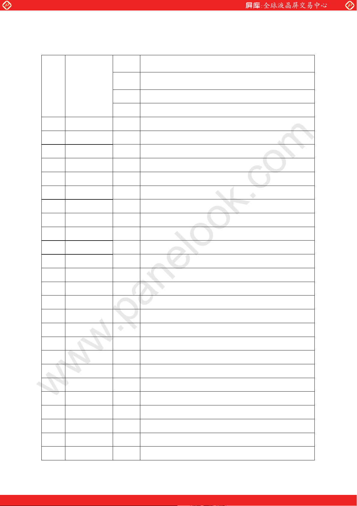
Version Revise Date Page Content
Cover-
1
17/Jun./1999
page
www.panelook.com
Record of Revision
”Tentative” Ш ”Preliminary”
2 20/Sep./1999
3 1. DF-19KR-20P-1H Ш DF-19K-20P-1H
5 1. 30msЉT2І70ms Ш 0ЉT2І70ms
1. Lamp voltage:650Vrms(Typ.) Ш 62062Vrms
9
2. Lamp starting voltage:1100Vrms Ш 1050Vrms(at 25к)
1500Vrms Ш 1260Vrms
14
1. CN1 connector pin assignment.
1 CN1 20 20 CN1 1
2. T-type rib of back side be cancelled.
Cover-
page
“UP133X01” Ш “UB133X01”
1. Weight: 49010(Typ.) Ш 50010(Typ.) 2
2. Thickness:5.5(typ) Ш 5.9(max)
4 1. Note1:80% Ш 90%
5 1. I
=(270mA)typ Ш IA=(350mA)typ, IB=(550mA)max
CC
at 0к
8 1. t
10
, t
: 600ps Ш 500ps
SU1
h1
1. Lamp voltage: 62062Vrms Ш 61061Vrms 9
2. Lamp starting voltage: 1050Vrms Ш 925Vrms(at 25к)
1260Vrms Ш 1530Vrms
1. White uniformity: 2.0max Ш 1.8max
2. CIE color: adding the R,G,B CIE color spec
1. Thermal cycling:2hrs, 30mins, 2hrs Ш 1H,10mins,1H 11
2. Vibration:10Hz~55Hz~10HzШ10Hz~500Hz~10Hz
13 Adding the packing form drawing
14
3 30/Sep./1999 14~15
Update the mechanical drawing
Update the mechanical drawing
4 07/Oct./1999 15 Update the mechanical drawing
5 10/Dec./1999
8 Correct the position ID to match the timing drawing
10 By : 0.1100.03 Ш 0.1200.03
at 0к
14~15
One step solution for LCD / PDP / OLED panel application: Datasheet, inventory and accessory!
Update the mechanical drawing
www.panelook.com
Page 3
Global LCD Panel Exchange Center
www.panelook.com
6 07/Apr./2000
7 30/Sep./2002 14 Updated Drawing
15 Updated Drawing
Cover
13
SPEC No:233-220-063 Ш 413-212-030
5 30msЉ T1І 70msec Ш 0msЉ T1І 70msec.
9 Lamp current: 3 ~ 6 ~ 6.5 mA Ш 2 ~ 5 ~ 6.5 mA
EPP package introduced
One step solution for LCD / PDP / OLED panel application: Datasheet, inventory and accessory!
www.panelook.com
Page 4

Global LCD Panel Exchange Center
www.panelook.com
SPEC NO. : 413-212-030
PAGE : 1/16
Contents:
A. Physical specificationˁˁˁˁˁˁˁˁˁˁˁˁˁˁˁˁˁˁˁˁˁˁˁˁˁˁˁˁˁˁˁˁˁˁˁˁˁˁˁˁˁˁˁˁˁˁˁˁˁˁˁˁˁ
B. Electrical specifications
1. Pin assignment
2. Absolute maximum ratingsˁˁˁˁˁˁˁˁˁˁˁˁˁˁˁˁˁˁˁˁˁˁˁˁˁˁˁˁˁˁˁˁˁˁˁˁˁˁˁˁˁˁˁˁˁˁˁˁˁˁ
3. Electrical characteristicsˁˁˁˁˁˁˁˁˁˁˁˁˁˁˁˁˁˁˁˁˁˁˁˁˁˁˁˁˁˁˁˁˁˁˁˁˁˁˁˁˁˁˁˁˁˁˁˁˁˁˁˁ
a. Typical operating conditionsˁˁˁˁˁˁˁˁˁˁˁˁˁˁˁˁˁˁˁˁˁˁˁˁˁˁˁˁˁˁˁˁˁˁˁˁˁˁˁˁˁˁˁˁˁ
b. Display color v.s. input data
signals
ˁˁˁˁˁˁˁˁˁˁˁˁˁˁˁˁˁˁˁˁˁˁˁˁˁˁˁˁˁˁˁˁˁˁˁˁˁˁˁ
c. Input signal timingˁˁˁˁˁˁˁˁˁˁˁˁˁˁˁˁˁˁˁˁˁˁˁˁˁˁˁˁˁˁˁˁˁˁˁˁˁˁˁˁˁˁˁˁˁˁˁˁˁˁˁ
ˁˁˁˁˁˁˁˁˁˁˁˁˁˁˁˁˁˁˁˁˁˁˁˁˁˁˁˁˁˁˁˁˁˁˁˁˁˁˁˁˁˁˁˁˁˁˁˁˁˁˁˁˁˁˁˁˁˁˁˁ
ˁˁˁˁˁˁˁˁˁˁˁˁˁˁˁˁˁˁˁˁˁˁˁˁˁˁˁˁˁˁˁˁˁˁˁˁˁˁˁˁˁˁˁˁˁˁˁˁˁˁˁ
P2
P3
P3
P4
P5
P5
P6
P7
d. Display positionˁˁˁˁˁˁˁˁˁˁˁˁˁˁˁˁˁˁˁˁˁˁˁˁˁˁˁˁˁˁˁˁˁˁˁˁˁˁˁˁˁˁˁˁˁˁˁˁˁˁˁˁˁˁ
e. Backlight driving conditions
C. Optical
specifications
D. Reliability test items
ˁˁˁˁˁˁˁˁˁˁˁˁˁˁˁˁˁˁˁˁˁˁˁˁˁˁˁˁˁˁˁˁˁˁˁˁˁˁˁˁˁˁˁˁˁˁˁˁˁˁˁˁˁˁ
ˁˁˁˁˁˁˁˁˁˁˁˁˁˁˁˁˁˁˁˁˁˁˁˁˁˁˁˁˁˁˁˁˁˁˁˁˁˁˁˁˁˁˁˁˁˁˁˁˁˁˁˁˁˁˁ
E. Display
quality
ˁˁˁˁˁˁˁˁˁˁˁˁˁˁˁˁˁˁˁˁˁˁˁˁˁˁˁˁˁˁˁˁˁˁˁˁˁˁˁˁˁˁˁˁˁˁˁˁˁˁˁˁˁˁˁˁˁˁˁ
F. Handling precaution
G. Packing form
ˁˁˁˁˁˁˁˁˁˁˁˁˁˁˁˁˁˁˁˁˁˁˁˁˁˁˁˁˁˁˁˁˁˁˁˁˁˁˁˁˁˁˁˁˁˁˁˁˁˁˁˁˁˁˁˁˁˁˁˁˁˁˁ
ˁˁˁˁˁˁˁˁˁˁˁˁˁˁˁˁˁˁˁˁˁˁˁˁˁˁˁˁˁˁˁˁˁˁˁˁˁˁˁˁˁ
ˁˁˁˁˁˁˁˁˁˁˁˁˁˁˁˁˁˁˁˁˁˁˁˁˁˁˁˁˁˁˁˁˁˁˁˁˁˁˁˁˁˁˁˁˁˁˁˁˁˁˁ
P8
P9
P10
P12
P12
P12
P13
Appendix:
Fig.1-(a) LCM outline dimensions(Front side)ˁˁˁˁˁˁˁˁˁˁˁˁˁˁˁˁˁˁˁˁˁˁˁˁˁˁˁˁˁˁˁˁˁˁˁ
Fig.1-(b) LCM outline dimensions (Back side)ˁˁˁˁˁˁˁˁˁˁˁˁˁˁˁˁˁˁˁˁˁˁˁˁˁˁˁˁˁˁˁˁˁˁˁ
Fig.2 Timing chartˁˁˁˁˁˁˁˁˁˁˁˁˁˁˁˁˁˁˁˁˁˁˁˁˁˁˁˁˁˁˁˁˁˁˁˁˁˁˁˁˁˁˁˁˁˁˁˁˁˁˁˁˁˁˁˁˁˁˁˁˁ
P14
P15
P16
ALL RIGHTS STRICTLY RESERVED. ANY PORTION OF THIS PRPER SHALL NOT BE REPRODUCED, COPIED, OR
TRANSFORMED TO ANY OTHER FORMS WITHOUT PERMISSION FROM UNIPAC OPTOELECTRONICS CORP.
One step solution for LCD / PDP / OLED panel application: Datasheet, inventory and accessory!
www.panelook.com
Page 5
Global LCD Panel Exchange Center
www.panelook.com
SPEC NO. : 413-212-030
PAGE : 2/16
A. Physical specifications
NO. Item Specification Remark
1 Display resolution(pixel)
2 Active area(mm)
3 Screen size(inch) 13.3(Diagonal)
4 Pixel pitch(mm)
5 Color configuration R. G. B. Vertical stripe
6 Overall dimension(mm)
7 Weight(g)
8 Surface treatment Hard coating(3H), anti-glare of the front
1024(H)768(V)
270.3(H)202.8(V)
0.264(H)0.264(V)
284(W)214.5(H)5.9 max(D)
50010
polarizer(12%)
Note 1: Refer to Fig. 1.
ALL RIGHTS STRICTLY RESERVED. ANY PORTION OF THIS PRPER SHALL NOT BE REPRODUCED, COPIED, OR
TRANSFORMED TO ANY OTHER FORMS WITHOUT PERMISSION FROM UNIPAC OPTOELECTRONICS CORP.
Note 1
One step solution for LCD / PDP / OLED panel application: Datasheet, inventory and accessory!
www.panelook.com
Page 6

Global LCD Panel Exchange Center
(
)
www.panelook.com
SPEC NO. : 413-212-030
PAGE : 3/16
B. Electrical specifications
1.Pin assignment
(1).Input signal interface
CN1 (20P) connector : DF-19K-20P-1H(Hirose)
User’s matching connector : DF19G-20S-1C(Wire type)
DF19-20S-1F
Pin no Symbol Function Etc.
1 VCC +3.3 V power supply
2 VCC +3.3 V power supply
3 GND Ground
4 GND Ground
5 RxIN0-
6 RxIN0+
7 GND Ground
8 RxIN1-
9 RxIN1+
10 GND Ground
11 RxIN2-
12 RxIN2+
13 GND Ground
14 CKIN-
15 CKIN+
16 GND Ground
17 NC No Connection
18 NC No Connection
19 GND Ground
20 GND Ground
ALL RIGHTS STRICTLY RESERVED. ANY PORTION OF THIS PRPER SHALL NOT BE REPRODUCED, COPIED, OR
TRANSFORMED TO ANY OTHER FORMS WITHOUT PERMISSION FROM UNIPAC OPTOELECTRONICS CORP.
LVDS receiver signal channel 0
LVDS receiver signal channel 1
LVDS receiver signal channel 2
LVDS receiver signal clock
FPC type
One step solution for LCD / PDP / OLED panel application: Datasheet, inventory and accessory!
www.panelook.com
Page 7

Global LCD Panel Exchange Center
www.panelook.com
SPEC NO. : 413-212-030
PAGE : 4/16
(2) LVDS transmitter/receiver signal mapping
Symbol Function
TxIN0 R0 Red data (LSB)
TxIN1 R1 Red data
TxIN2 R2 Red data
TxIN3 R3 Red data
TxIN4 R4 Red data
TxIN5 R5 Red data (MSB)
TxIN6 G0 Green data (LSB)
TxIN7 G1 Green data
TxIN8 G2 Green data
TxIN9 G3 Green data
TxIN10 G4 Green data
TxIN11 G5 Green data (MSB)
TxIN12 B0 Blue data (LSB)
TxIN13 B1 Blue data
TxIN14 B2 Blue data
TxIN15 B3 Blue data
TxIN16 B4 Blue data
TxIN17 B5 Blue data (MSB)
TxIN18 Hs Horizontal sync
TxIN19 Vs Vertical sync
TxIN20 DE Data enable
TxCLKIN CLK Clock Dot clock
2. Absolute maximum ratings (GND = 0 V)
6 bit red display data
6 bit green display data
6 bits blue display data
Parameter Symbol
Power voltage VCC -0.3 4 VDC
Input signal voltage VLH -0.3 VCC+0.3 VDC
Operating temperature Top 0 +50
Storage temperature TST -20 +60
Values
Min. Max.
Unit
к
к
Note 1:The relative humidity must not exceed 90% non-condensing at temperatures of 40к or
less. At temperatures greater than 40к, the wet bulb temperature must not exceed 39
к. When operate at low temperatures, the brightness of CCFL will drop and the life
time of CCFL will be reduced.
Note 2:The unit should not be exposed to corrosive chemicals.
ALL RIGHTS STRICTLY RESERVED. ANY PORTION OF THIS PRPER SHALL NOT BE REPRODUCED, COPIED, OR
TRANSFORMED TO ANY OTHER FORMS WITHOUT PERMISSION FROM UNIPAC OPTOELECTRONICS CORP.
One step solution for LCD / PDP / OLED panel application: Datasheet, inventory and accessory!
Remark
At 25к
At 25к
Note 1
Note 1
www.panelook.com
Page 8

Global LCD Panel Exchange Center
SFO
%
p
www.panelook.com
SPEC NO. : 413-212-030
PAGE : 5/16
3. Electrical characteristics
a. Typical operating conditions
Item Symbol Min. Typ. Max. Unit Remark
Power
supply
voltage
Internal
logic
Power ripple voltage
Note 1:Effective value (mArms) at VCC = 3.3 V/25к.
Note 2: Refer to the following power-on condition.
Power
Input signal
Apply the lamp voltage within the LCD operating range. When the backlight turns on before
the LCD operation or the LCD turns off before the backlight turns off, the display may
momentaily become abnormal.
ALL RIGHTS STRICTLY RESERVED. ANY PORTION OF THIS PRPER SHALL NOT BE REPRODUCED, COPIED, OR
TRAN
RMED TO ANY OTHER FORMS WITHOUT PERMISSION FROM UNIPAC OPTOELECTRONICS CORP.
Input voltage VCC 3.0 3.3 3.6 V
Current
consumption
Inrush current I
Low voltage
High voltage
I
A
White
64 Grayscale
IA - 350 -
- - 550 mArms
I
B
- - 2200 mApeak Note 2
RUSH
0 - 0.3 VCC
V
IL
0.7VCC - VCC
V
IH
- - 100 mVp-p
V
RP
I
B
Black
10
Vertical stri
=
e line
Black
( 0 )
64
Gray
( 7 )
64
Sequence of Power-on/off and signal-on/off
T3
0msЉT1І70msec
T2T1
T5
0ЉT2І70msec
300msecЉT3
300msecЉT4
Note 1
One step solution for LCD / PDP / OLED panel application: Datasheet, inventory and accessory!
www.panelook.com
Page 9

Global LCD Panel Exchange Center
www.panelook.com
Caution
SPEC NO. : 413-212-030
PAGE : 6/16
The above on/off sequence should be applied to avoid abnormal function in the display.
In case of handling:
Make sure to turn off the power when you plug the cable into the input connector or pull the
cable out of the connector.
b. Display color v.s. input data signals
Display colors
Basic
colors
Red
grayscale
Green
grayscale
Blue
grayscale
Black
Blue
Red
Magenta
Green
Cyan
Yellow
White
Black
Dark
Х
Ц
bright
Red
Black
Dark
Х
Ц
bright
Green
Black
Dark
Х
Ц
bright
Blue
R5 R4 R3 R2 R1 R0 G5 G4 G3 G2 G1 G0 B5 B4 B3 B2 B1 B0
0
0
0
0
0
0
1
1
1
1
1
1
0
0
0
0
0
0
1
1
1
1
1
1
0
0
0
0
0
0
0
0
0
1
1
1
1
1
1
1
1
1
0
0
0
0
0
0
0
0
0
0
0
0
0
0
0
0
0
0
0
0
0
0
0
0
0
0
0
0
0
0
0
0
0
0
0
0
Data signal (0 : Low level, 1: High level)
0
0
0
0
0
0
0
0
0
0
0
0
0
0
0
0
0
0
0
0
0
1
1
1
0
0
0
0
0
1
1
1
1
1
1
1
1
0
0
0
1
1
1
1
1
0
0
0
1
1
1
1
1
1
1
1
1
1
1
1
1
1
1
1
0
0
0
0
0
0
0
0
0
0
0
0
0
1
0
0
0
0
0
0
0
0
1
0
0
0
0
0
0
1
0
1
0
0
0
0
0
0
1
1
0
0
0
0
0
1
1
1
0
0
0
0
0
0
0
0
0
0
0
0
0
0
0
0
0
0
0
1
1
1
0
0
0
1
1
1
0
0
0
1
1
1
0
0
0
0
0
0
0
0
0
0
0
0
0
0
0
0
0
0
0
0
0
0
0
0
0
0
0
0
0
0
0
0
0
0
0
0
0
0
0
0
0
0
0
1
1
0
1
1
1
1
0
0
0
0
0
0
0
0
0
0
0
0
0
0
1
0
0
0
1
0
0
1
1
1
1
0
1
1
0
0
0
0
0
0
0
0
0
0
0
0
0
0
0
1
0
0
0
1
0
0
0
1
0
0
0
0
0
0
0
1
0
1
0
1
0
0
1
1
0
0
1
1
0
0
1
1
0
0
1
1
0
0
0
0
0
0
0
0
0
0
0
0
0
0
0
0
0
0
0
0
0
0
0
0
0
0
0
0
0
0
1
1
1
1
1
1
0
0
1
1
0
0
1
1
0
0
1
1
0
0
1
1
0
0
0
0
0
0
0
0
0
0
0
0
0
0
0
0
0
0
0
0
0
0
0
0
0
0
0
0
1
0
0
1
1
1
1
1
Note : Each basic color can be displayed in 64 gray scales using the 6 bit data signals. By
combining the 18-bit data signals(R,G,B), the 262, 144 colors can be achieved on the
display.
ALL RIGHTS STRICTLY RESERVED. ANY PORTION OF THIS PRPER SHALL NOT BE REPRODUCED, COPIED, OR
TRANSFORMED TO ANY OTHER FORMS WITHOUT PERMISSION FROM UNIPAC OPTOELECTRONICS CORP.
0
1
0
1
0
1
0
1
0
0
0
0
0
0
0
0
0
0
0
0
0
1
0
1
0
1
One step solution for LCD / PDP / OLED panel application: Datasheet, inventory and accessory!
www.panelook.com
Page 10

Global LCD Panel Exchange Center
www.panelook.com
c. Input signal timing
Timing diagrams of input signal are shown in Fig 2.
(1). Timing characteristics of input signals
CLK clock
Horizontal
Vertical
Available data input timing
Horizontal
Hs
sync
Vs
sync
Item Symbol Min. Typ.Max.Unit Remark
Frequency Fck 50 65 66 MHz
Period Clk 20 15.4 15.2 ns
1040 1344 1648 Clk Period Th
20 20.7 - Ӵs
Display period Thd 1024 Clk
Pulse width Thw 2 136 - Clk
296 296 296 Clk Display start The
8 296 600 Clk
Front porch Thf 8 24 - Clk
Back porch Thb 4 160 - Clk
Blanking Thb1 16 320 624 Th
Phase shift Tvpd 2 320 - Clk
803 806 895 Th Period Tv
- 16.6 20 ms
Display width Tvd 768 Th
Pulse width Tvw 1 6 - Th
Display start Tve - 35 - Th DE non-using
Front porch Tvf 0 3 - Th
Blanking Tvb1 35 38 127 Th
DE non-using When DE signal is fixed Low, after falling edge of Hs, counting 296
clocks, then getting valid data from 297th
SPEC NO. : 413-212-030
PAGE : 7/16
DE non-using
DE using
clock’s data.
DE using Valid data is according to rising edge of “DE” signal.
The time should be 8 to 600 clocks between falling edge of Hs and
rising edge of DE.
Vertical
DE non-using After falling edge of Vs, counting 35 Th, then getting 36th Th’s
data. (in DE non-using mode and DE using mode).
DE using Valid data is according to the first rising edge of “DE” signal after
DE keeps low during blanking period.
ALL RIGHTS STRICTLY RESERVED. ANY PORTION OF THIS PRPER SHALL NOT BE REPRODUCED, COPIED, OR
TRANSFORMED TO ANY OTHER FORMS WITHOUT PERMISSION FROM UNIPAC OPTOELECTRONICS CORP.
One step solution for LCD / PDP / OLED panel application: Datasheet, inventory and accessory!
www.panelook.com
Page 11

Global LCD Panel Exchange Center
A
www.panelook.com
SPEC NO. : 413-212-030
PAGE : 8/16
(2). The timing condition of LVDS
Item Symbol Min. Typ. Max. Unit
The differential level ΨVIDΨ 0.1 - 0.6 V
VID
Ϊ
The common mode input voltage VIC
The input setup time tsu1 500 - - ps
The input hold time th1 500 - - ps
Ϊ
2
-
2.4Ё
Ϊ
VID
Ϊ
2
V
V
ID
VID = V
IAP
- V
IAM
V
IAP
V
IAM
th1 tsu1
n
7LCK
d.Display position
D( 1,1 ) D( 2,1 ) …… D( X,1 ) …… D( 1023,1 ) D( 1024,1 )
D( 1,2 ) D( 2,2 ) …… D( X,2 ) …… D( 1023,2 ) D( 1024,2 )
.
.
.
D( 1,Y ) D( 2,Y ) …… D( X,Y ) …… D( 1023,Y ) D( 1024,Y )
.
.
.
D( 1,767 ) D( 2,767 ) …… D( X,767 ) …… D( 1023,767) D( 1024,767
D( 1,768 ) D( 2,768 ) …… D( X,768 ) …… D( 1023,768 D( 1024,768
……
……
.
.
.
.
.
.
……
……
.
.
.
.
.
.
.
.
.
.
.
.
ALL RIGHTS STRICTLY RESERVED. ANY PORTION OF THIS PRPER SHALL NOT BE REPRODUCED, COPIED, OR
TRANSFORMED TO ANY OTHER FORMS WITHOUT PERMISSION FROM UNIPAC OPTOELECTRONICS CORP.
One step solution for LCD / PDP / OLED panel application: Datasheet, inventory and accessory!
www.panelook.com
Page 12

Global LCD Panel Exchange Center
SFO
www.panelook.com
e.Backlight driving conditions
Parameter Symbol Min. Typ. Max. Unit Remark
Lamp voltage VL 549 610 671 Vrms I
Lamp current
Power consumption
Lamp starting voltage VS
Frequency FL 50 60 80 KHZ Note 3
Lamp life time LL 10000 - - Hr Note 4
Note 1: Using the inverter of PWM type(keep stable peak value of output voltage during
adjusting lamp current), the minimum lamp current is 2mA.
Note 2: Inverter should be designed with the characteristic of lamp. When you are designing
(1).The area under the positive and negative cycles of the waveform of the lamp
current and lamp voltage should be area symmetric(the symmetric ratio should be
larger than 90%).
(2).There should not have any spikes in the waveform.
(3).The waveform should be sine wave as possible.
(4).Lamp current should not exceed the maximum value within the operating
temperature (It is prohibited to over the maximum lamp current even if operated in
the non-guaranteed temperature). When lamp current over the maximum value for
a long time, it may cause fire. Therefore, it is recommend that the inverter should
have the current limiter circuit.
Note 3: Lamp frequency may produce interference with horizontal synchronous frequency
and
this may cause line flow on the display. Therefore lamp frequency shall be
detached
from the horizontal synchronous frequency and its harmonics as far as possible in
order to avoid interference. In case using the inverter by PWM control, PWM
Note 4: T= 25к, I
Note 5: CN2 connector(backlight): BHSR-02VS-1(JST).
Mating connector: SM02B-BHSS-1-TB (JST).
Pin no. Symbol Function Remark
1 H CCFL power supply(H.V.) Cable color: Pink
2 L CCFL power supply(GND) Cable color: White
the inverter, the output voltage of the inverter should comply with the following
conditions.
frequency may interference with frame frequency. We suggest that PWM frequency
is same as frame frequency.
IL 2 5 6.5 mArms Note 1
= 6mA. Brightness to be decrease to the 50% of the initial value.
L
PL 3.66 W Note 2
- - 1530 T=0к
- - 925
SPEC NO. : 413-212-030
PAGE : 9/16
Vrms
= 6mA.
L
T=25
к
ALL RIGHTS STRICTLY RESERVED. ANY PORTION OF THIS PRPER SHALL NOT BE REPRODUCED, COPIED, OR
TRAN
One step solution for LCD / PDP / OLED panel application: Datasheet, inventory and accessory!
RMED TO ANY OTHER FORMS WITHOUT PERMISSION FROM UNIPAC OPTOELECTRONICS CORP.
www.panelook.com
Page 13

Global LCD Panel Exchange Center
C. Optical specifications ( Note 1, Note 2, Note 3 )
Item Symbol Condition
Response time
Rising time
Falling time
Contrast ratio CR
Viewing angle
To p
Bottom
Left
Right
Brightness(5 points)
Color chromaticity(CIE)
White uniformity
Note 1: Ambient temperature = 25к.
Note 2: To be measured in dark room after backlight warm up 30 minutes.
Note 3: To be measured with a viewing cone of 1by Topcon luminance meter BM-5A.
Note 4: Definition of response time:(To be measured by Topcon BM-5A)
The output signals of photodetector are measured when the input signals are changed
from “Black” to “White” (falling time) and from “White” to “Black” (rising time),
respectively. The response time interval between the 10% and 90% of amplitudes. Refer
to figure as below.
YL
Wx
Wy
Rx
Ry
Gx
Gy
Bx
By
Ӭ
www.panelook.com
Tr
Tf
W
Ӱ=0
Ӱ=0
CRЊ10
Ӱ=0
Ӱ=0
- - 1.8 Note 9
SPEC NO. : 413-212-030
PAGE
Specification
Min. Typ. Max.
-
-
150 200 - Note 5
10
30
40
40
100 130 - nit Note 6,7,9
0.280 0.310 0.340
0.300 0.330 0.360
0.547 0.577 0.607
0.298 0.328 0.358
0.270 0.300 0.330
0.545 0.575 0.605
0.115 0.145 0.175
0.090 0.120 0.150
20
30
-
-
-
-
40
60
-
-
-
-
10/16
:
Unit Remark
ms Note 4
deg. Note 8
"Black"
100%
S
ig
90%
n
a
l(
R
e
la
t
i
v
e
v
a
lu
10%
e
)
0%
Tr
Tf
"White""White"
One step solution for LCD / PDP / OLED panel application: Datasheet, inventory and accessory!
www.panelook.com
Page 14

Global LCD Panel Exchange Center
p
f
)
(
G
C
ALL RIGHTS STRICTLY RESERVED. ANY PORTION OF THIS PRPER SHALL NOT BE REPRODUCED, COPIED, OR
TRANSFORMED TO ANY OTHER FORMS WITHOUT PERMISSION FROM UNIPAC OPTOELECTRONICS CORP.
Note 5. Definition of contrast ratio:
Contrast ratio is calculated with the following formula.
Note 6: Definition of brightness:
Note 7: Driving conditions for CCFT : I
Note 8: Definition of viewing angle(To be measure at display center by LCD-7000):
Contrast ratio (CR)=
Brightness(
Y
)=
L
www.panelook.com
Photodetector output when LCD is at “White” state
Photodetector out
YLD +YLE +YLG +YLI +Y
5
= 6.0 mA
L
ut when LCD is at “Black” state
LJ
SPEC NO. : 413-212-030
PAGE
:
11/16
LJ
Note 9: Definition of white uniformity:
White uniformity is defined as the following with thirteen measurements (A~M).
Ӭ
ALL RIGHTS STRICTLY RESERVED. ANY PORTION OF THIS PRPER SHALL NOT BE REPRODUCED, COPIED, OR
TRANSFORMED TO ANY OTHER FORMS WITHOUT PERMISSION FROM UNIPAC OPTOELECTRONICS CORP.
W
A
D
F
I
Maximum Luminance o
=
Minimum Luminance of thirteen points(brightness)
512 768256 98638
B
E
H
L
M
thirteen points(brightness
38
192
384
576
LINES)
730
One step solution for LCD / PDP / OLED panel application: Datasheet, inventory and accessory!
www.panelook.com
Page 15

Global LCD Panel Exchange Center
judg
(
)
(
,
(
(
SFO
www.panelook.com
SPEC NO. : 413-212-030
PAGE
:
12/16
D. Reliability test items(Note 1)
Test tem Test Condition
High temperature storage
Low temperature storage
High temperature & high
humidity operation
High temperature operation
Low temperature operation
Temperature cycling
non-operation)
Electrostatic discharge
non-operation)
Vibration
(non-operation)
Mechanical shock
non-operation)
60к, 240Hrs
-20к, 240Hrs
40к, 90%RH, 240Hrs
No condensation
50к, 240Hrs
0к, 240Hrs
-20к~60к
10mins, 1H, 5cycles
1H
150PF, 150Ө, 10KV, 1second, 9
points on the panel, 10 times each place
Sweep:1G, 10HZ ~ 500HZ ~ 10HZ /2.5min
2 hour for each direction X, Y, Z
(6 Hrs in total)
50G, 11ms, X, Y, Z
once for each direction
Note 1: Evaluation should be tested after storage at room temperature for one hour.
Note 2: There should be no change which might affect the practical display function when the
display quality test is conducted under normal operating condition.
Note 3: The discharging points are shown as below.
ement Remark
Display quality Note 1, 2
Display quality Note 1, 2
Display quality Note 1, 2
Display quality Note 1, 2
Display quality Note 1, 2
Display quality Note 1, 2
Display function Note 3
Display quality Note 1, 2
Display quality Note 1, 2
E. Display quality
The display quality of the color TFT-LCD module should be in compliance with the
unipac’s Incoming inspection standard.
F. Handling precaution
The Handling of the TFT-LCD should be in compliance with the Unipac’s handling principle
standard.
ALL RIGHTS STRICTLY RESERVED. ANY PORTION OF THIS PRPER SHALL NOT BE REPRODUCED, COPIED, OR
TRAN
RMED TO ANY OTHER FORMS WITHOUT PERMISSION FROM UNIPAC OPTOELECTRONICS CORP.
One step solution for LCD / PDP / OLED panel application: Datasheet, inventory and accessory!
www.panelook.com
Page 16

Global LCD Panel Exchange Center
SFO
G. Packing form
LCD Module
www.panelook.com
SPEC NO. : 413-212-030
PAGE
:
13/16
Anti-Static Bag
Note :
1.The panel of each LCD Module faces toward
seperation pad.
2.Max. capacity : 20 LCD Modules/Carton.
3.Max. weight : 14.6kg/Carton.
4.Meas. : 458mm*412mm*365mm.
Note 1.
Separate Pad
2
Cushion
Carton
1
ALL RIGHTS STRICTLY RESERVED. ANY PORTION OF THIS PRPER SHALL NOT BE REPRODUCED, COPIED, OR
TRAN
One step solution for LCD / PDP / OLED panel application: Datasheet, inventory and accessory!
RMED TO ANY OTHER FORMS WITHOUT PERMISSION FROM UNIPAC OPTOELECTRONICS CORP.
www.panelook.com
Page 17

Global LCD Panel Exchange Center
www.panelook.com
SPEC NO. : 413-212-030
PAGE
:
14/16
ALL RIGHTS STRICTLY RESERVED. ANY PORTION OF THIS PRPER SHALL NOT BE REPRODUCED, COPIED, OR
TRANSFORMED TO ANY OTHER FORMS WITHOUT PERMISSION FROM UNIPAC OPTOELECTRONICS CORP.
One step solution for LCD / PDP / OLED panel application: Datasheet, inventory and accessory!
Fig.1-(a) LCM outline dimensions (Front side)
www.panelook.com
Page 18

Global LCD Panel Exchange Center
SFO
www.panelook.com
SPEC NO. : 413-212-030
PAGE : 15/16
ALL RIGHTS STRICTLY RESERVED. ANY PORTION OF THIS PRPER SHALL NOT BE REPRODUCED, COPIED, OR
TRAN
One step solution for LCD / PDP / OLED panel application: Datasheet, inventory and accessory!
RMED TO ANY OTHER FORMS WITHOUT PERMISSION FROM UNIPAC OPTOELECTRONICS CORP.
Fig.1-(b) LCM outline dimensions (Back side)
www.panelook.com
Page 19

Global LCD Panel Exchange Center
SFO
www.panelook.com
)
k
c
lo
c
/
l
e
x
i
p
1
lid
a
v
d
f
li
v
a
v
T
n
I
8
6
7
,
X
7
6
7
,
X
d
v
T
v
T
h
T
3
,
X
2
,
X
1
,
X
h
T
in
f
h
T
Y
,
4
2
0
1
Y
,
3
2
0
1
Y
,
3
Y
,
2
Y
,
1
(
d
h
T
SPEC NO. : 413-212-030
PAGE : 16/16
l
c
T
h
c
T
s
h
h
h
T
T
,
,
s
h
e
e
T
T
,
,
s
h
d
d
T
T
H
H
L
L
I
I
I
I
V
V
V
V
s
K
H
L
,
C
E
D
,
B
G
R
Fig.2 Timing chart
b
h
T
l
b
v
T
w
h
T
E
D
s
H
e
h
T
f
h
T
K
L
C
l
b
lid
h
a
T
v
in
Y
,
4
2
0
1
L
H
I
I
V
V
d
p
v
T
L
H
I
I
V
V
B
G
R
E
D
s
s
H
V
e
v
T
lid
a
v
n
w
v
T
I
f
v
T
8
6
7
,
X
7
6
7
,
X
B
G
s
s
V
R
H
ALL RIGHTS STRICTLY RESERVED. ANY PORTION OF THIS PRPER SHALL NOT BE REPRODUCED, COPIED, OR
TRAN
RMED TO ANY OTHER FORMS WITHOUT PERMISSION FROM UNIPAC OPTOELECTRONICS CORP.
One step solution for LCD / PDP / OLED panel application: Datasheet, inventory and accessory!
www.panelook.com
 Loading...