

Page 1
Global LCD Panel Exchange Center
www.panelook.com
Document Version: 1
Date: 2004/09/24
Product Functional Specification
12.1 inch Wide XGA Color TFT LCD Module
Model Name: A121EW01 V0
( Ϭ) Preliminary Specification
( ) Final Specification
Note: This Specification is subject to change without notice.
(C) Copyright AU Optronics
Jul., 2004 All Rights Reserved. A121EW01 V0
No Reproduction and Redistribution Allowed.
18
1/18
One step solution for LCD / PDP / OLED panel application: Datasheet, inventory and accessory!
www.panelook.com
Page 2

Global LCD Panel Exchange Center
www.panelook.com
Contents
1.0 Handling Precautions ....................................................................................................................... 4
2.0 General Description............................................................................................................................ 5
2.1 Display Characteristics ...................................................................................................................... 5
2.2 Functional Block Diagram.................................................................................................................. 6
3.0 Absolute Maximum Ratings............................................................................................................... 7
4.0 Optical Characteristics....................................................................................................................... 8
5.0 Signal Interface ................................................................................................................................... 8
5.1 Connectors .......................................................................................................................................... 8
5.2 Signal Pin............................................................................................................................................. 8
5.3 Signal Description .............................................................................................................................. 9
5.4 Signal Electrical Characteristics ..................................................................................................... 10
5.5 Signal for Lamp connector .............................................................................................................. 10
6.0 Pixel Format Image ........................................................................................................................... 11
7.0 Parameter guide line for CCFL Inverter .......................................................................................... 11
8.0 Timing
Control………………………………………………………………………………………………….14
8.1 Timing Characteristics ..................................................................................................................... 13
8.2 Timing Definition............................................................................................................................... 13
9.0 Power Consumption ......................................................................................................................... 14
10. Power ON/OFF Sequence................................................................................................................. 15
11.0 Reliability /Safety Requirement ..................................................................................................... 16
12.0 Outline drawing…………………………………………………………………………………………….18
(C) Copyright AU Optronics
Jul., 2004 All Rights Reserved. A121EW01 V0
No Reproduction and Redistribution Allowed.
18
2/18
One step solution for LCD / PDP / OLED panel application: Datasheet, inventory and accessory!
www.panelook.com
Page 3
Global LCD Panel Exchange Center
www.panelook.com
II Record of Revision
Version and Date Page Old description New Description Remark
V1. 2004/07/23 All First Release NA
V2. 2004/09/20 17-18 Physical Size:
275.11(W) x 184.39(H) x 8.8(D)
V2. 2004/09/20 5 Physical Size:
275.11(W) x 184.39(H) x 8.8(D)
Physical Size
276.7(W) x 184.7(H) x 8.8(D)
Physical Size
276.7(W) x 184.7(H) x 8.8(D)
(C) Copyright AU Optronics
Jul., 2004 All Rights Reserved. A121EW01 V0
No Reproduction and Redistribution Allowed.
18
3/18
One step solution for LCD / PDP / OLED panel application: Datasheet, inventory and accessory!
www.panelook.com
Page 4

Global LCD Panel Exchange Center
www.panelook.com
1.0 Handling Precautions
1) Do not press or scratch the surface harder than a HB pencil lead because the polarizers are very fragile
and could be easily damaged.
2) Be sure to turn off power supply when inserting or disconnecting from input connector.
3) Wipe off water droplets or oil immediately. Long contact with the droplets may cause discoloration or
spots.
4) When the panel surface is soiled, wipe it with absorbent cotton or other soft cloth.
5) Since the panel is made of glass, it may break or crack if dropped or bumped on hard surface.
6) Protect the module from static electricity and insure proper grounding when handling. Static electricity
may cause damage to the CMOS Gate Array IC.
7) Do not disassemble the module.
8) Do not press the reflector sheet at the back of the module.
9) Avoid damaging the TFT module. Do not press the center of the CCFL Reflector when it was taken out
from the packing container. Instead, press at the edge of the CCFL Reflector softly.
10) Do not rotate or tilt the signal interface connector of the TFT module when you insert or remove other
connector into the signal interface connector.
11) Do not twist or bend the TFT module when installation of the TFT module into an enclosure (Notebook
PC Bezel, for example). It should be taken into consideration that no bending/twisting forces are applied
to the TFT module from outside when designing the enclosure. Otherwise the TFT module may be
damaged.
12) Cold cathode fluorescent lamp in LCD contains a small amount of mercury. Please follow local regulations for
disposal.
13) The LCD module contains a small amount of material that has no flammability grade, so it should be supplied
by power complied with requirements of limited power source (2.11, IEC60950 or UL1950).
14) The CCFL in the LCD module is supplied with Limited Current Circuit (2.4, IEC60950 or UL1950). Do not
connect the CCFL in Hazardous Voltage Circuit.
(C) Copyright AU Optronics
Jul., 2004 All Rights Reserved. A121EW01 V0
No Reproduction and Redistribution Allowed.
18
4/18
One step solution for LCD / PDP / OLED panel application: Datasheet, inventory and accessory!
www.panelook.com
Page 5
Global LCD Panel Exchange Center
www.panelook.com
2.0 General Description
This specification applies to the 12.1 inch wide Color TFT/LCD Module A121EW01 V0
This module is designed for a display unit of Portable Video Devices.
The screen format is intended to support the XGA (1280(H) x 800(V)) screen and 262k colors (RGB 6-bits data
driver).
All input signals are LVDS interface compatible.
This module does not contain an inverter card for backlight.
22..11DDiissppllaayyCChhaarraacctteerriissttiiccs
The following items are characteristics summary on the table under 25 к condition:
ITEMS Unit SPECIFICATIONS
Screen Diagonal [mm] 307.9(12.1" wide)
Active Area [mm] 261.12(H) x163.2 (V)
Pixels H x V 1280(x3) x 800
Pixel Pitch [mm] 0.204 x 0.204
Pixel Arrangement R.G.B. Vertical Stripe
Display Mode Normally White
Typical White Luminance(CCFL=6.0mA) [cd/m2] 450 Typ.
Contrast Ratio 350:1
Response Time [msec] 25 Typ.
Nominal Input Voltage VDD [Volt] +3.3 Typ.
Weight [Grams] 550g typ.
Physical Size [mm] 276.7(W) x 184.7(H) x 8.8(D) Max.
Electrical Interface LVDS
Color Depth 262K colors
Temperature Range
Operating
Storage (Shipping)
s
o
C]
[
o
C]
[
0 to +60
-40 to +65
(C) Copyright AU Optronics
Jul., 2004 All Rights Reserved. A121EW01 V0
No Reproduction and Redistribution Allowed.
18
5/18
One step solution for LCD / PDP / OLED panel application: Datasheet, inventory and accessory!
www.panelook.com
Page 6
Global LCD Panel Exchange Center
p
)
www.panelook.com
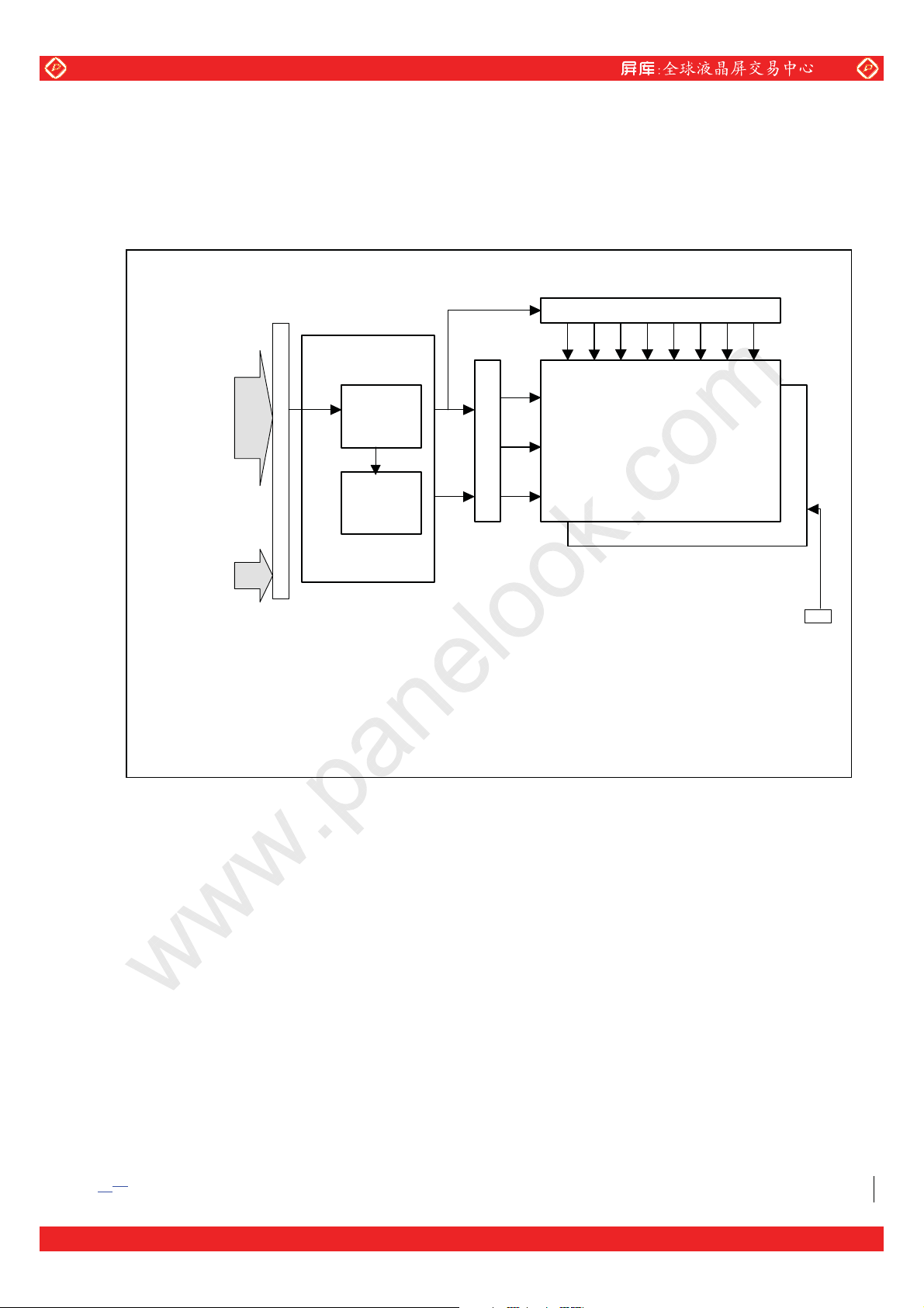
22..22FFuunnccttiioonnaallBBlloocckkDDiiaaggrraam
m
The following diagram shows the functional block of the 12.1 inches Color TFT/LCD Module:
X-Driver
(4 pairs LVDS)
RxIN0
RxIN1
RxIN2
RxCLKIN
VDD
GND
Hirose DF19K-20P-1H
Mating Type DF19G-20S-1C
LCD DRIVE
CARD
LCD
Controller
DC-DC
Converter
Ref circuit
Y-Dri ver
TFT ARRAY/CELL
1280 x 3 x 800
Backlight Unit
Lam
Connector(2pin
JST BHSR-02VS-1
Mating Type SM02B-BHSS-1-TB
(C) Copyright AU Optronics
Jul., 2004 All Rights Reserved. A121EW01 V0
No Reproduction and Redistribution Allowed.
18
6/18
One step solution for LCD / PDP / OLED panel application: Datasheet, inventory and accessory!
www.panelook.com
Page 7

Global LCD Panel Exchange Center
www.panelook.com
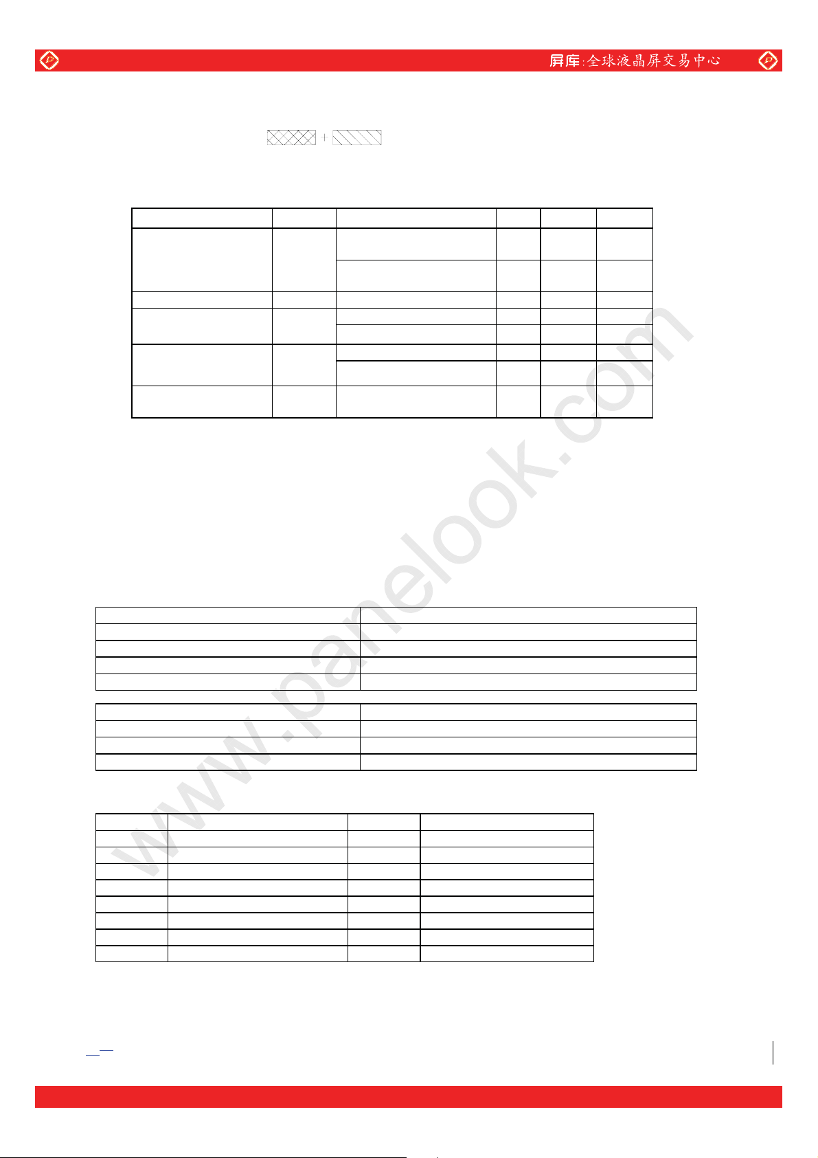
3.0 Absolute Maximum Ratings
Absolute maximum ratings of the module is as following:
Item Symbol Min Max Unit Conditions
Logic/LCD Drive Voltage VDD -0.3 +4.0 [Volt]
Input Voltage of Signal Vin -0.3 VDD+0.3 [Volt]
CCFL Current ICFL - 7 [mA] rms
CCFL Ignition Voltage Vs - TBD(25oC) Vrms Note 1
Operating Temperature TOP 0 +60 [oC] Note 2
Operating Humidity HOP 5 95 [%RH] Note 2
Storage Temperature TST -25 +65 [oC]
Storage Humidity HST 5 95 [%RH] Note 2
Vibration 1.5, 10-500 [G Hz]
Shock 200, 3 [G ms] Half sine wave
Note 1 : Duration = 3sec
Note 2 : Maximum Wet-Bulb should be 39к and No condensation.
Wet bulb temperature chart
Twb=39°C
Operating Range
(C) Copyright AU Optronics
Jul., 2004 All Rights Reserved. A121EW01 V0
No Reproduction and Redistribution Allowed.
18
7/18
One step solution for LCD / PDP / OLED panel application: Datasheet, inventory and accessory!
www.panelook.com
Page 8
Global LCD Panel Exchange Center
www.panelook.com
Storage Range
4.0 Optical Characteristics
The optical characteristics are measured under stable conditions as follows under 25к condition:
Item
Viewing Angle [degree]
CR: Contrast Ratio [degree]
Contrast ratio 300 350 Response Time [msec] Rising - 10 15
Color / Chromaticity White x 0.26 0.31 0.36
Coordinates (CIE)
Unit
[degree]
[degree]
[msec] Falling - 15 20
Conditions Min. Typ. Max.
Horizontal (Right)
CR = 10 (Left)
Vertical (Upper)
CR = 10 (Lower)
White y
50
50
40
50
0.28 0.33 0.38
65
65
50
65
-
-
-
-
White Luminance
CCFL @ 6.0mA
[cd/m2] Central 380 450 -
5.0 Signal Interface
55..11CCoonnnneeccttoorrs
Physical interface is described as for the connector on module.
These connectors are capable of accommodating the following signals and will be following components.
Connector Name / Designation
Manufacturer
Type / Part Number
Mating Housing/Part Number
Mating Contact/Part Number
Connector Name / Designation
Manufacturer
Type / Part Number
Mating Type / Part Number
s
For Signal Connector
Hirose
DF19K-20P-1H
DF19G-20S-1C
DF19-2830 SCFA
For Lamp Connector
JST
BHSR-02VS-1
SM02B-BHSS-1-TB
55..22SSiiggnnaallPPiin
Pin# Signal Name Pin# Signal Name
1 VDD 2 VDD
3 GND 4 GND
5 RxIN0- 6 RxIN0+
7 GND 8 RxIN1-
9 RxIN1+ 10 GND
11 RxIN2- 12 RxIN2+
13 GND 14 RxCLKIN15 RxCLKIN+ 16 GND
(C) Copyright AU Optronics
Jul., 2004 All Rights Reserved. A121EW01 V0
No Reproduction and Redistribution Allowed.
18
8/19
One step solution for LCD / PDP / OLED panel application: Datasheet, inventory and accessory!
n
www.panelook.com
Page 9

Global LCD Panel Exchange Center
www.panelook.com
17 V
19 CLK
55..33SSiiggnnaallDDeessccrriippttiioon
EDID
EDID
n
18 NC
20 DATA
EDID
The module uses a LVDS receiver embedded in AUO’s ASIC. LVDS is a differential signal technology for LCD
interface and high-speed data transfer device.
Signal Name
Description
RxIN0-, RxIN0+ LVDS differential data input(Red0-Red5, Green0)
RxIN1-, RxIN1+ LVDS differential data input(Green1-Green5, Blue0-Blue1)
RxIN2-, RxIN2+ LVDS differential data input(Blue2-Blue5, Hsync, Vsync, DSPTMG)
RxCLKIN-, RxCLKIN0+ LVDS differential clock input
VDD +3.3V Power Supply
GND Ground
Note: Input signals shall be in low status when VDD is off.
Internal circuit of LVDS inputs are as following.
Signal Name Description
+RED5
+RED4
+RED3
+RED2
+RED1
+RED0
Red Data 5 (MSB)
Red Data 4
Red Data 3
Red Data 2
Red Data 1
Red Data 0 (LSB)
Red-pixel Data
Each red pixel's brightness data consists of these 6 bits
pixel data.
Red-pixel Data
+GREEN 5
+GREEN 4
+GREEN 3
+GREEN 2
+GREEN 1
+GREEN 0
Green Data 5 (MSB)
Green Data 4
Green Data 3
Green Data 2
Green Data 1
Green Data 0 (LSB)
Green-pixel Data
Each green pixel's brightness data consists of these 6 bits
pixel data.
Green-pixel Data
+BLUE 5
+BLUE 4
+BLUE 3
+BLUE 2
+BLUE 1
+BLUE 0
Blue Data 5 (MSB)
Blue Data 4
Blue Data 3
Blue Data 2
Blue Data 1
Blue Data 0 (LSB)
Blue-pixel Data
Each blue pixel's brightness data consists of these 6 bits
pixel data.
Blue-pixel Data
-DTCLK
Data Clock
The typical frequency is 65.0 MHz. The signal is used to
strobe the pixel data and DSPTMG signals. All pixel data
shall be valid at the falling edge when the DSPTMG signal
is high.
DSPTMG
Display Timing
This signal is strobed at the falling edge of
-DTCLK. When the signal is high, the pixel data shall be
valid to be displayed.
VSYNC
HSYNC
Vertical Sync
Horizontal Sync
The signal is synchronized to -DTCLK .
The signal is synchronized to -DTCLK .
Note: Output signals from any system shall be low or Hi-Z state when VDD is off.
(C) Copyright AU Optronics
Jul., 2004 All Rights Reserved. A121EW01 V0
No Reproduction and Redistribution Allowed.
18
9/19
One step solution for LCD / PDP / OLED panel application: Datasheet, inventory and accessory!
www.panelook.com
Page 10
Global LCD Panel Exchange Center
www.panelook.com
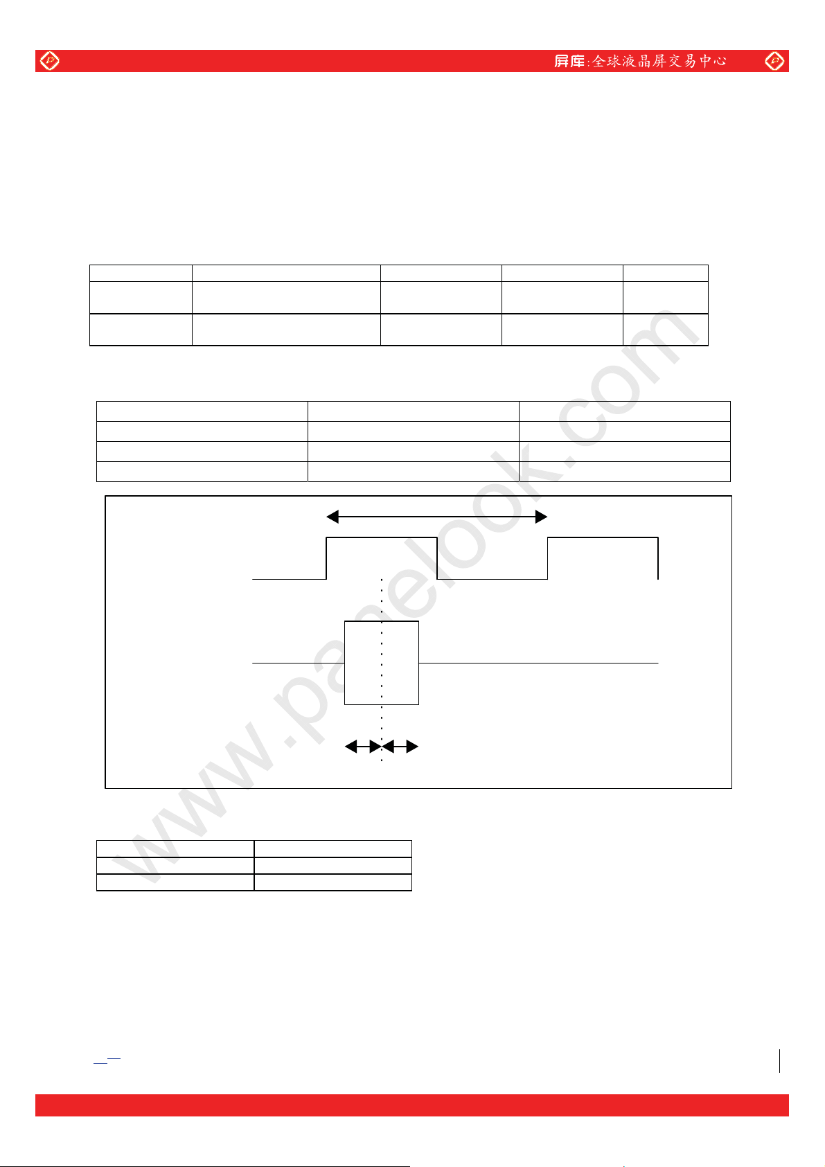
55..44SSiiggnnaallEElleeccttrriiccaallCChhaarraacctteerriissttiiccs
Input signals shall be in low status when VDD is off.
It is recommended to refer the specifications of SN75LVDS86DGG (Texas Instruments) in detail.
Signal electrical characteristics are as follows;
Parameter Condition Min Max Unit
Differential Input High
Vth
Vtl
LVDS Macro AC characteristics are as follows:
Clock Frequency (F) 20MHz 85MHz
Data Setup Time (Tsu) 600ps
Data Hold Time (Thd) 600ps
Voltage(Vcm=+1.2V) 100 [mV]
Differential Input Low
Voltage(Vcm=+1.2V) -100 [mV]
s
Min. Max.
T
Input Clock
Input Data
ThdTsu
55..55SSiiggnnaallffoorrLLaammppccoonnnneeccttoor
Pin # Signal Name
1 Lamp High Voltage
2 Lamp Low Voltage
(C) Copyright AU Optronics
Jul., 2004 All Rights Reserved. A121EW01 V0
No Reproduction and Redistribution Allowed.
18
10/19
r
One step solution for LCD / PDP / OLED panel application: Datasheet, inventory and accessory!
www.panelook.com
Page 11
Global LCD Panel Exchange Center
!
!
www.panelook.com
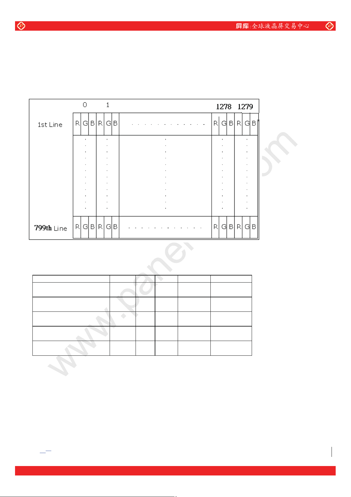
6.0 Pixel Format Image
Following figure shows the relationship of the input signals and LCD pixel format.
7.0 Parameter guide line for CCFL Inverter
Parameter Min
CCFL current(ICFL) 6.0 7.0 [mA] rms
CCFL Frequency(FCFL) 50 70 [KHz]
CCFL Ignition Voltage(Vs) TBD
CCFL Voltage (Reference)
(VCFL)
Single CCFL Power
consumption (PCFL)
Note 1: DP-1 are AUO recommended Design Points.
*1 All of characteristics listed are measured under the condition using the AUO Test inverter.
*2 In case of using an inverter other than listed, it is recommended to check the inverter carefully. Sometimes,
interfering noise stripes appear on the screen, and substandard luminance or flicker at low power may happen.
*3 In designing an inverter, it is suggested to check safety circuit ver carefully. Impedance of CCFL, for instance,
becomes more than 1 [M ohm] when CCFL is damaged.
*4 Generally, CCFL has some amount of delay time after applying start-up voltage. It is recommended to keep
on applying start-up voltage for 1 [Sec] until discharge.
(C) Copyright AU Optronics
Jul., 2004 All Rights Reserved. A121EW01 V0
No Reproduction and Redistribution Allowed.
18
11/18
DP-1 Max
TBD
TBD
Units Condition
[Volt] rms
[Volt] rms
[Watt]
(Ta=25к)
Note 2
(Ta=25к)
Note 3
(Ta= 0к)
Note 4
(Ta=25к)
Note 5
(Ta=25к)
Note 5
One step solution for LCD / PDP / OLED panel application: Datasheet, inventory and accessory!
www.panelook.com
Page 12

Global LCD Panel Exchange Center
www.panelook.com
*5 The CCFL inverter operating frequency must be carefully chosen so that no interfering noise stripes on the
screen were induced.
*6 Reducing CCFL current increases CCFL discharge voltage and generally increases CCFL discharge
frequency. So all the parameters of an inverter should be carefully designed so as not to produce too much
leakage current from high-voltage output of the inverter.
Note 2: It should be employed the inverter, which has “Duty Dimming”, if ICCFL is less than 4mA.
Note 3: The CCFL inverter operating frequency should be carefully determined to avoid interference between
inverter and TFT LCD.
Note 4: The inverter open voltage should be designed larger than the lamp starting voltage at T=0
o
C, otherwise
backlight may be blinking for a moment after turning on or not be able to turn on. The open voltage should
be measured after ballast capacitor. If an inverter has shutdown function it should keep its open voltage. for
longer than 1 second even if lamp connector is open.
Note 5: Calculator value for reference (ICFL×VCFL=PCFL)
(C) Copyright AU Optronics
Jul., 2004 All Rights Reserved. A121EW01 V0
No Reproduction and Redistribution Allowed.
18
12/18
One step solution for LCD / PDP / OLED panel application: Datasheet, inventory and accessory!
www.panelook.com
Page 13
Global LCD Panel Exchange Center
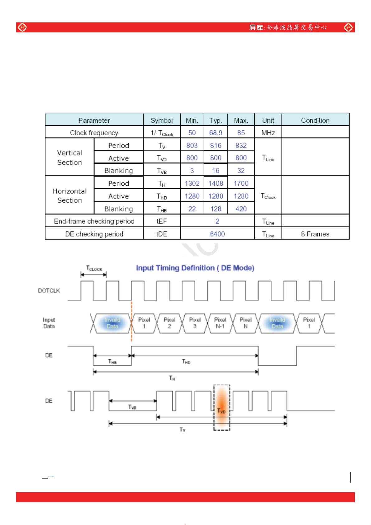
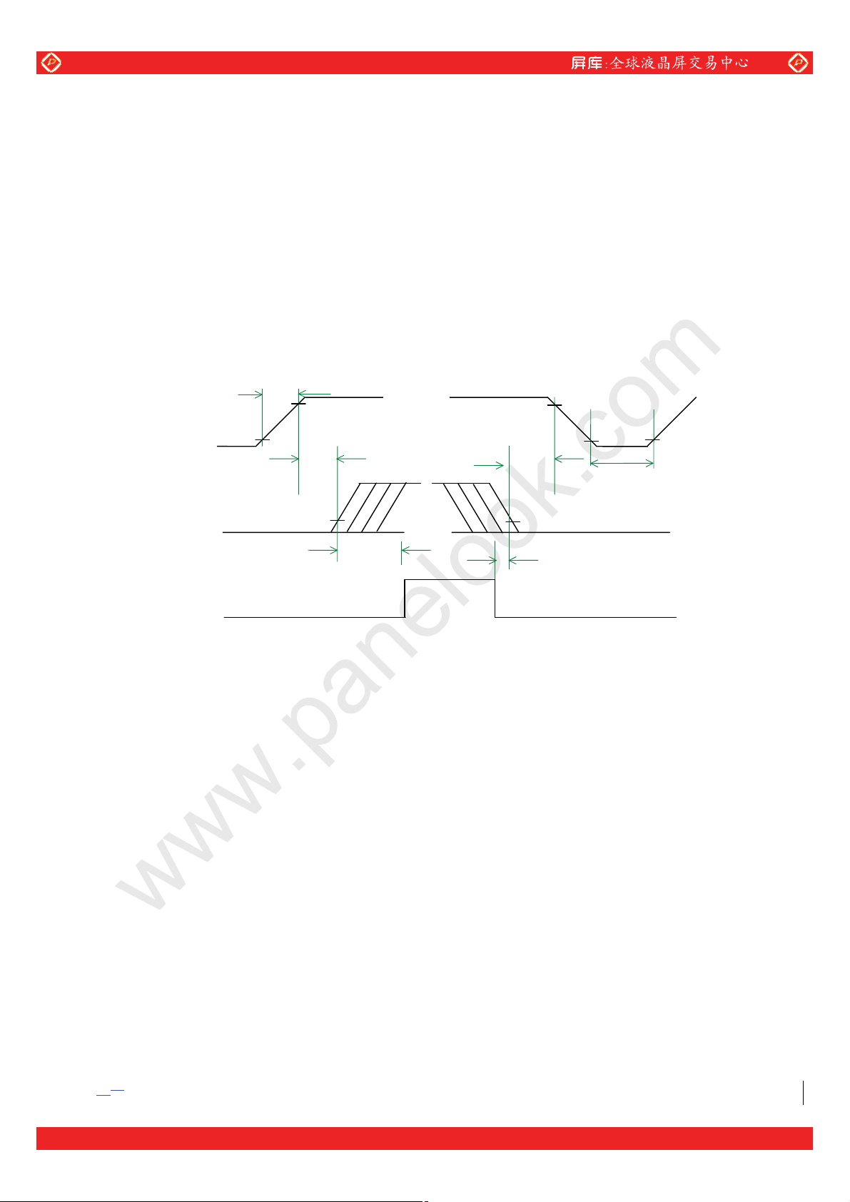
8.0 Timing Control
www.panelook.com
88..11TTiimmiinnggCChhaarraacctteerriissttiiccs
This is the signal timing required at the input of the user connector . All of the interface signal timing should be satisfied with
the following specifications .
88..22TTiimmiinnggDDeeffiinniittiioon
n
s
(C) Copyright AU Optronics
Jul., 2004 All Rights Reserved. A121EW01 V0
No Reproduction and Redistribution Allowed.
18
13/18
One step solution for LCD / PDP / OLED panel application: Datasheet, inventory and accessory!
www.panelook.com
Page 14

Global LCD Panel Exchange Center
www.panelook.com
9.0 Power Consumption
Input power specifications are as follows;
Symbol Parameter Min Typ Max Units Condition
Module
VDD Logic/LCD Drive
Voltage
PDD VDD Power 1.6 [Watt] All Black Pattern
PDD Max VDD Power max 1.7 [Watt]
IDD IDD Current 400 mA 64 Grayscale Pattern
IDD Max IDD Current max 420 mA Vertical stripe line Pattern
VDDrp Allowable
Logic/LCD Drive
Ripple Voltage
VDDns Allowable
Logic/LCD Drive
Ripple Noise
Lamp (Single Lamp Features) (Note 2)
ICFL CCFL current 4.0 6.0 7.0 [mA]
VCFL CCFL Voltage
(Reference)
VSCFL CCFL Starting
Voltage (Reference)
PCFL CCFL Power
consumption
3.0 3.3 3.6 [Volt] Load Capacitance 20uF
Max Pattern (Note 1)
(Note 1)
500 [mV]
p-p
100 [mV]
p-p
(Ta=25к)
rms
TBD
TBD
TBD
[Volt]
rms
[Volt]
rms
[Watt]
(Ta=25к)
(Ta=25к)
(Ta=25к)
Note 1: VDD=3.3V
Note 2: A121EW01 V0 Module includes dual lamps
(C) Copyright AU Optronics
Jul., 2004 All Rights Reserved. A121EW01 V0
No Reproduction and Redistribution Allowed.
18
14/18
One step solution for LCD / PDP / OLED panel application: Datasheet, inventory and accessory!
www.panelook.com
Page 15
Global LCD Panel Exchange Center
www.panelook.com
10. Power ON/OFF Sequence
VDD power and lamp on/off sequence is as follows. Interface signals are also shown in the chart. Signals
from any system shall be Hi-Z state or low level when VDD is off.
Sequence of Power-on/off and signal-on/off
Power Supply VDD
LVDS Interface
Backlight On
0.1VDD
T1
0.9VDD
T5
0.9VDD
T6
0.1VDD
T3T2
0.5msЉT1Љ10ms
0msЉT2Љ50ms
0msЉT3І50ms
500msЉT4
200msЉT5
200msЉT6
Apply the lamp voltage within the LCD operating range. When the backlight turns on before the
LCD operation or the LCD turns off before the backlight turns off, the display may momentarily
become abnormal.
(C) Copyright AU Optronics
Jul., 2004 All Rights Reserved. A121EW01 V0
No Reproduction and Redistribution Allowed.
18
15/18
One step solution for LCD / PDP / OLED panel application: Datasheet, inventory and accessory!
www.panelook.com
Page 16

Global LCD Panel Exchange Center
www.panelook.com
11.0 Reliability /Safety Requirement
RReelliiaabbiilliittyyTTeessttCCoonnddiittiioonns
Items Required Conditions
Operating Life – High Temp.
Operating Life – Low Temp.
High Temp. Storage Life – Non-Operating
Low Temp. Storage Life – Non-Operating
High Temp & High Humidity Operating Life
Shock – Non-Operating
Vibration – Non-Operating
Temp. Cycle – Operating
s
Temp.= +60qC, Dynamic. 250 Hours, Humidity 20%
Temp.= 0qC, Dynamic, 250 Hours, Humidity 20%
Temp.= +65qC, Non-Operating, 250 Hours, Humidity 20%
Temp.= -25qC, Non-Operating, 250 Hours
Temp.= +40qC, Dynamic, Humidity 95%(Non-Condensing),
250 Hours
220g’s, 2.0 ms, Half Sine Wave
r 3 Axis ( +X, -X, +Y, -Y, +Z, -Z)
3 Shocks per direction
1.5 Grms, 30 min/side, PSD Spectrum Break Points, 26
Hz G2/Hz=0.316, 50 Hz G2/Hz=0.007, 222 Hz
2
/Hz=0.0018, 500Hz G2/Hz=0.0001
G
0qC to+40qC, Ramp d20qC/min, Duration at Temp. =
30min, Test Cycles = 160
Temp. Cycle – Non-Operating
CCFL Life Time: 10,000 hours minimum
-25qC to +65qC, Ramp d20qC/min, Duration at Temp. =
30min, Test Cycles = 50
The” CCFL Life Time” is defined as the module brightness decrease to 50% original brightness at
Ta=25к, I
(C) Copyright AU Optronics
Jul., 2004 All Rights Reserved. A121EW01 V0
No Reproduction and Redistribution Allowed.
18
16/18
=6mA.
L
One step solution for LCD / PDP / OLED panel application: Datasheet, inventory and accessory!
www.panelook.com
Page 17

Global LCD Panel Exchange Center
12. Outline drawing
www.panelook.com
(C) Copyright AU Optronics
Jul., 2004 All Rights Reserved. A121EW01 V0
No Reproduction and Redistribution Allowed.
18
17/18
One step solution for LCD / PDP / OLED panel application: Datasheet, inventory and accessory!
www.panelook.com
Page 18

Global LCD Panel Exchange Center
www.panelook.com
(C) Copyright AU Optronics
Jul., 2004 All Rights Reserved. A121EW01 V0
No Reproduction and Redistribution Allowed.
18
18/18
One step solution for LCD / PDP / OLED panel application: Datasheet, inventory and accessory!
www.panelook.com
 Loading...