

Page 1

CHAPTER 2 HARDWARE INST ALLA TION
Chapter 2
HARDWARE INSTALLATION
2.1 Central Processing Unit: CPU
The A TX AL9 mainboard operates with Intel® Pentium® processor with
TM
MMX
processors. It could operate with 2.1V to 3.5V processors. The mainboard
provides a 321-pin ZIF Socket 7 for easy CPU installation, a jumper switch
(S1) to set the proper speed for the CPU and (S2) for setting the CPU
voltage. The CPU should always have a cooling fan attached to prevent
overheating.
2.1-1 CPU Installation Procedures
technology, Cyrix® 6x86L/6x86MX, and AMD® K6/K6-2/K6-III
1 . Pull the lever sideways away
from the socket. Then, raise
the lever up to a 90-degree
angle.
2 . Locate Pin 1 in the socket
and look for the white dot or
cut edge in the CPU. Match
Pin 1 with the white dot/cut
edge. Then, insert the CPU.
It should insert easily.
3. Press the lever down to
complete the installation.
2-1
Sliding
Plate
Open Lever
CPU
CPU
Close
Lever
Pin 1
White dot/
Cut edge
Page 2

CHAPTER 2 HARDWARE INST ALLA TION
2.1-2 CPU Core Speed Derivation Procedure
1. The Jumper S1 (4, 5 & 6) is used to adjust the CPU clock frequency.
4 5 6
000100
0 0 1 75*
01083
0 1 1 66
10095
1 0 1 68
11075**
1 1 1 60
* AGP = 60/PCI =30
** AGP = 75/PCI = 37.5
CPU
Clock
0 = Open 1 = Short
2-2
Page 3

CHAPTER 2 HARDWARE INST ALLA TION
2. The Jumper S1 (1, 2, and 3) is used to set the Core/Bus (Fraction) ratio of
the CPU. The actual core speed of the CPU is the Host Clock Frequency
multiplied by the Core/Bus ratio. For example:
If CPU Clock = 66MHz
Core/Bus ratio = 3/2
then CPU core speed = Host Clock x Core/Bus ratio
= 66MHz x 3/2
= 100MHz
1 2 3 CPU
0 0 0 1.5/3.5
0103x
1002x
1102.5x
0 0 1 5.5x
0 1 1 5x
1 0 1 4x
1 1 1 4.5x
Intel
AMD
Cyrix
IDT
AMD
K6/K6 2
0 = Open 1 = Short
2-3
Page 4
CHAPTER 2 HARDWARE INST ALLA TION
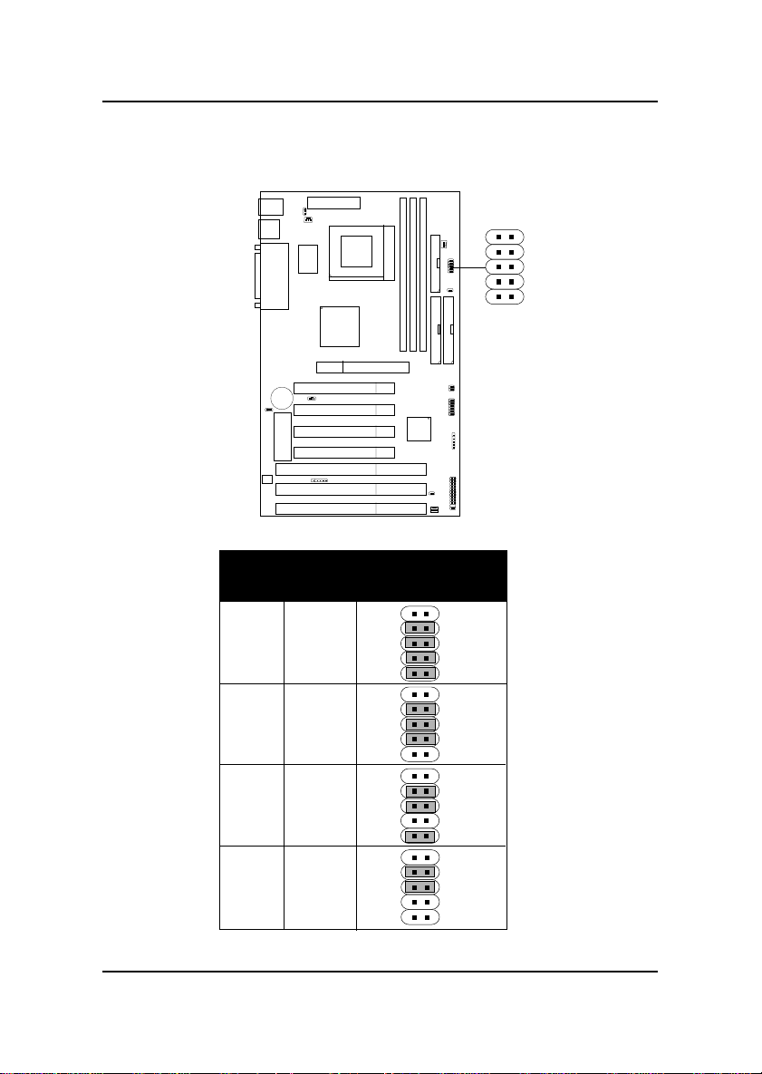
2.1-3 CPU Voltage Setting: S2
5
1
S2
VcoreV I/O
3.45 3.5
3.45
3.45
3.45
3.4
3.3
3.2
S2
5
1
5
1
5
1
5
1
2-4
Page 5
CHAPTER 2 HARDWARE INST ALLA TION
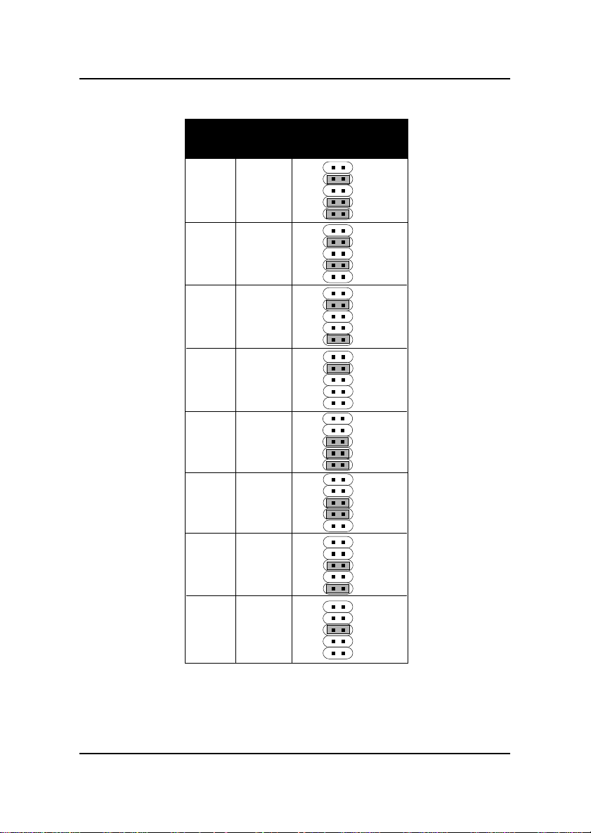
VcoreV I/O
3.45
3.45
3.45
3.45
3.1
3.0
2.9
2.8
3.45 2.7
3.45
3.45
2.6
2.5
S2
5
1
5
1
5
1
5
1
5
1
5
1
5
3.45
1
5
2.4
1
2-5
Page 6
CHAPTER 2 HARDWARE INST ALLA TION
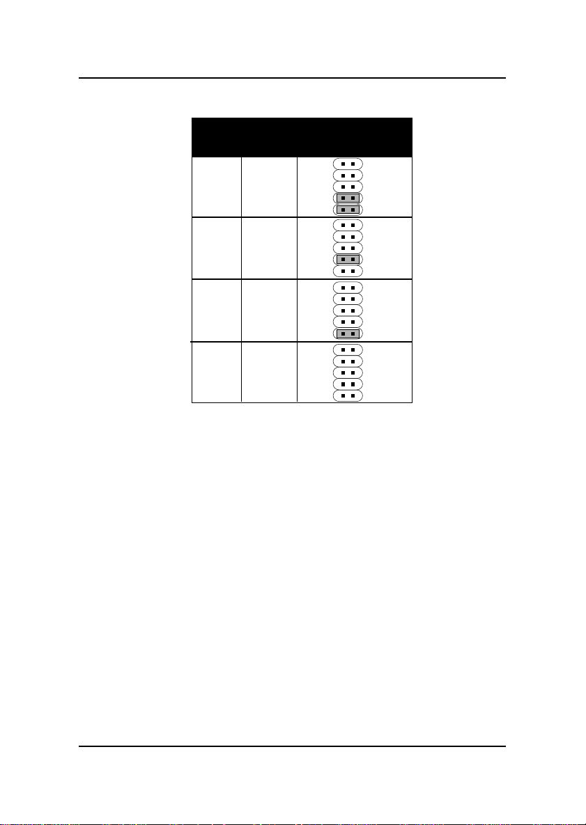
3.45
3.45
3.45
3.45
VcoreV I/O
S2
5
2.3
1
5
2.2
1
5
2.1
1
5
2.0
1
2-6
Page 7
CHAPTER 2 HARDWARE INST ALLA TION
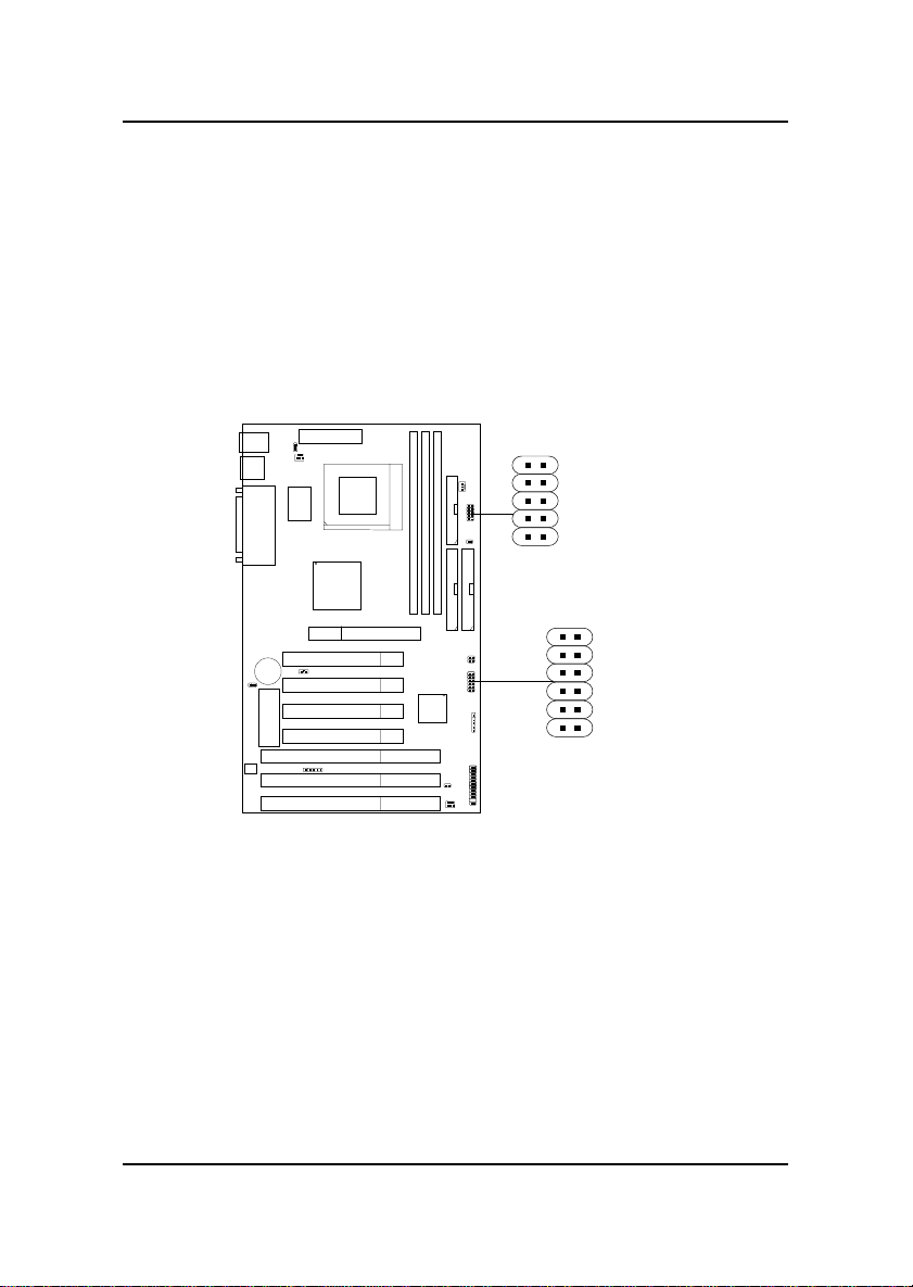
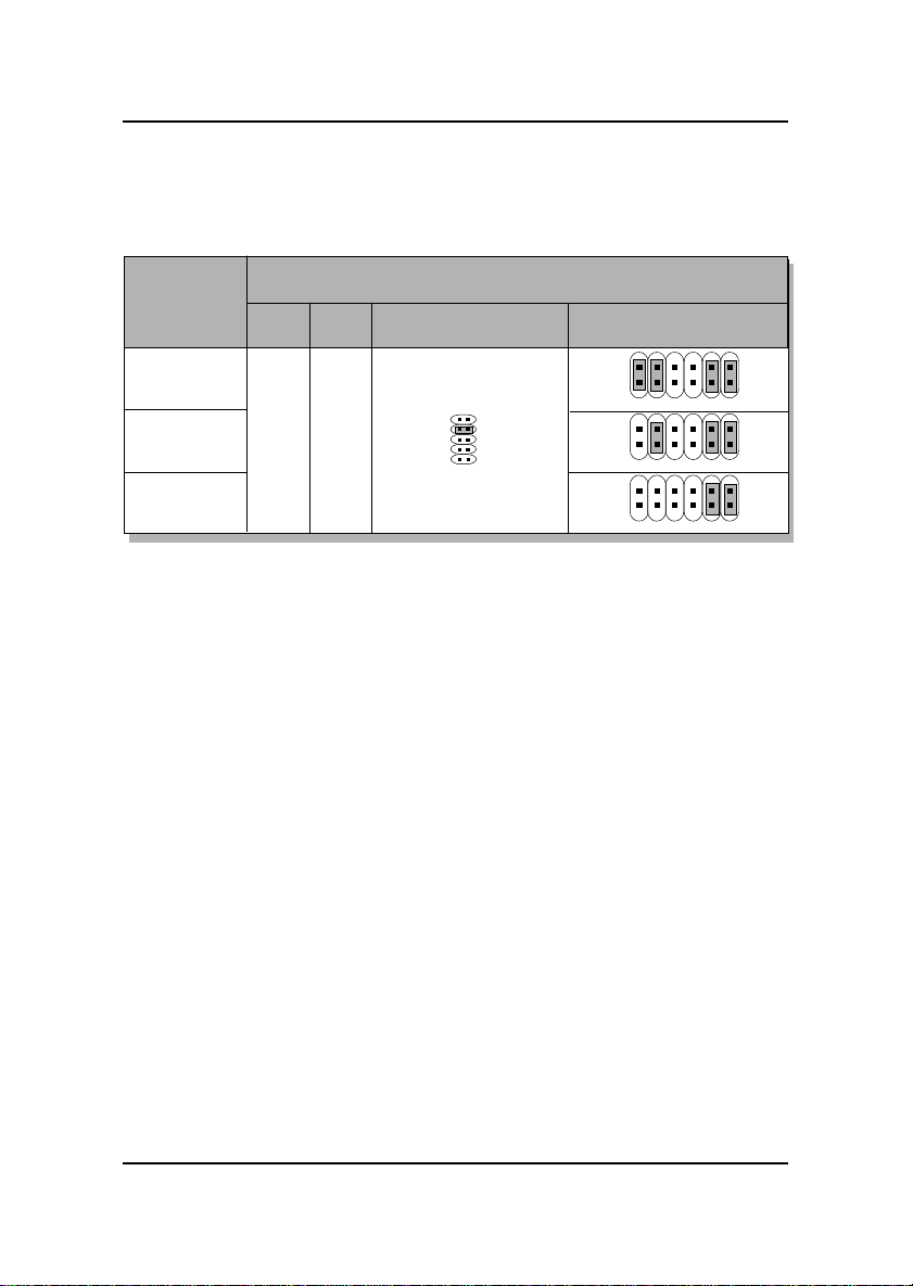
2.1-4 CPU Speed and Voltage Setting: S1 and S2
To set the proper speed and voltage of the CPU, you must know the specifications of your CPU (always ask the vendor for CPU specifications).
Then refer to Table 2.1 (Intel® Processor), Table 2.2 (Cyrix
Processor), Table 2.3 (AMD® Processor) and Table 2.4 (IDT C6TM) for
proper setting.
S2
S1
®
6
1
2-7
Page 8
CHAPTER 2 HARDWARE INST ALLA TION
Table 2.1 Intel® Processor
Intel® Pentium® Processor with MMX
TM
T echnology
CPU
Type
VI/O
Vcore
CPU SpeedCPU Voltage
S1S2
166 MHz
6
6
200 MHz
3.45
2.8
5
1
1
1
233MHz
1
Note: If you encounter a CPU with different voltage, just go to Section
2.1-3 and look for the proper voltage settings.
6
2-8
Page 9
CHAPTER 2 HARDWARE INST ALLA TION
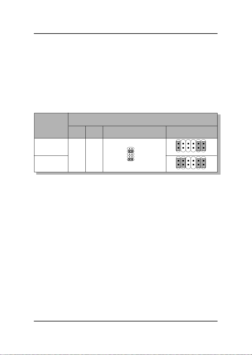
Table 2.2 Cyrix® Processor
Cyrix® 6x86 processor uses PR to rate the speed of their processors based
on Intel® Pentium® processor core speed. For example, PR150 (120MHz)
has 150MHz core speed of Intel® Pentium® processor, but it has120MHz
core speed in Cyrix® processor. Cyrix® 6x86 processor should always use a
more powerful fan (ask vendor for proper cooling fan).
a. Cyrix® 6x86/6x86L processor
CPU
Type
6x86L
PR166
6x86L
PR200
VI/O Vcore
3.45
2.9
S2
CPU SpeedCPU Voltage
S1
5
1
1
1
6
6
2-9
Page 10
CHAPTER 2 HARDWARE INST ALLA TION
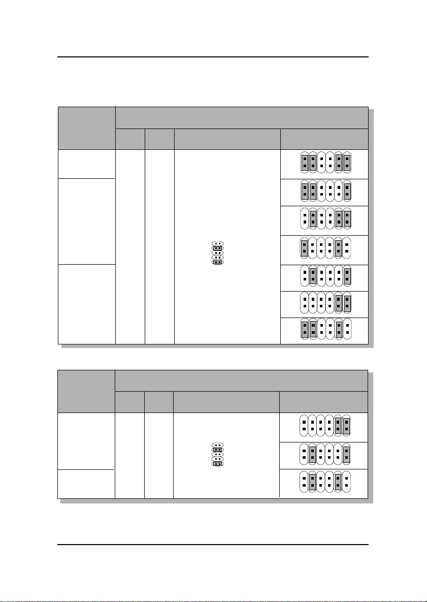
b. Cyrix® 6x86MX Processor
CPU
Type
PR200
(66 x 2.5)
PR233
(75 x 2.5)
(66 x 3)
(83 x 2)
PR266
(75 x3)
(66 x 3.5)
(83 x 2.5)
c. Cyrix® MII Processor
VI/O
3.45
Vcore
2.9
CPU
Type
VI/O
Vcore
CPU Voltage
S2
5
1
CPU Voltage
S2
CPU Speed
S1
1
1
1
1
1
1
1
6
6
6
6
6
6
6
CPU Speed
S1
PR300
(66 x 3.5)
(75 x 3)
3.45
2.9
5
1
1
1
PR333
(83 x 3)
1
Note: If you encounter a CPU with different voltage, just go to Section
2.1-3 and look for the proper voltage settings.
2-10
6
6
6
Page 11
CHAPTER 2 HARDWARE INST ALLA TION
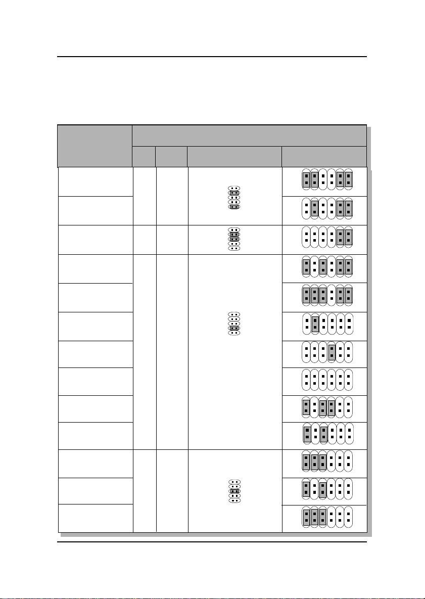
Table 2.3 AMD® Processor
AMD® K6/K6-2/K6-3 Processor
CPU
Type
VI/O
Vcore
S2
CPU SpeedCPU Voltage
S1
166MHz
200MHz
233MHz
266MHz
300MHz
K6-2 300MHz
K6-2 333MHz
K6-2 350MHz
K6-2 380MHz
K6-2 400MHz
K6-2 450MHz
K6-III 400MHz
K6-III 450MHz
3.45
3.45
3.45
3.45
2.9
3.2
2.2
2.4
5
1
5
1
5
1
5
1
1
1
1
1
1
1
1
1
1
1
1
1
1
6
6
6
6
6
6
6
6
6
6
6
6
6
2-11
Page 12
CHAPTER 2 HARDWARE INST ALLA TION
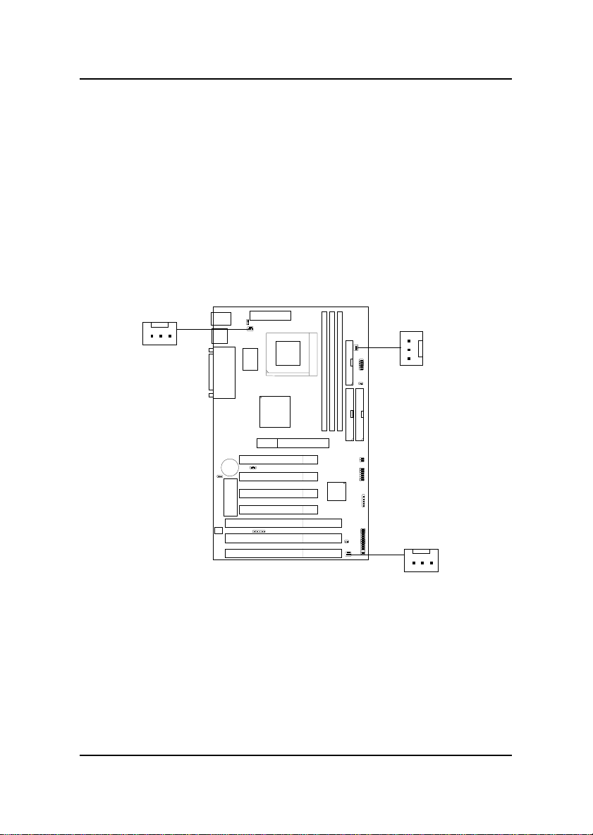
2.1-5 Fan Power Connectors: JFAN1, JSFAN1, & JPFAN1
These connectors support system cooling fan with +12V. It supports three
pin head connector. When connecting the wire to the connector, always
take note that the red wire is the positive and should be connected to the
+12V, the black wire is Ground and should be connected to GND. If your
mainboard has System Hardware Monitor chipset on-board, you can use a
specially designed fan w/ speed sensor to take advantage of System Hardware Monitor’s CPU fan control.
+12V
SPEED
JFAN1: CPU FAN
JPFAN1: POWER FAN
JSFAN1: CHASSIS FAN
GND
JSFAN1
SPEED
GND
+12V
SPEED
JFAN1
+12V
GND
JPFAN1
For fans with fan speed sensor, every rotation of the fan will send out 2
pulses. System Hardware Monitor will count and report the fan rotation
speed.
Note: Always consult vendor for proper CPU cooling fan.
2-12
Page 13
CHAPTER 2 HARDWARE INST ALLA TION
2.2 Memory Installation
2.2-1 Memory Bank Configuration
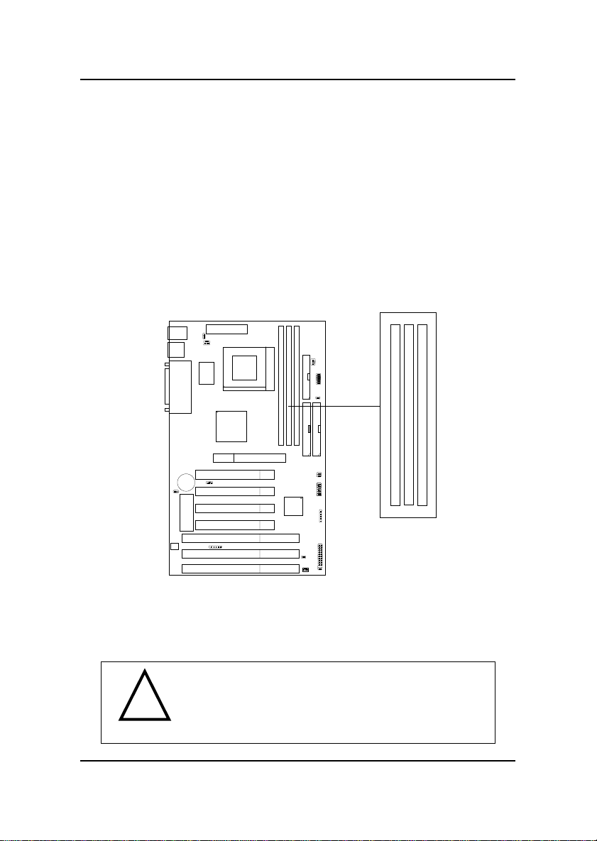
The mainboard provides three 168-pin DIMM(Double In-Line Memory)
sockets. It supports six memory banks for a maximum of 768MB memory.
You can use DIMM from 8MB, 16MB, 32MB, 64MB, 128MB to 256MB.
DIMM1(Bank 2/3)
DIMM3(Bank 0/1)
DIMM2(Bank 4/5)
!
WARNING!
If you use 100 MHz CPU Bus Frequency, only PC100
DIMM Specs. is supported.
2-13
Page 14
CHAPTER 2 HARDWARE INST ALLA TION
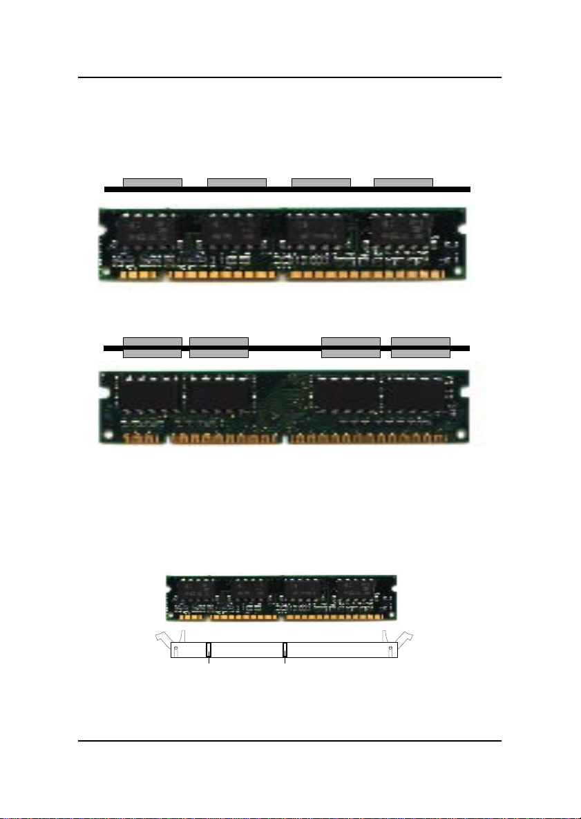
2.2-2 Memory Installation Procedures:
A. How to install DIMM Module
Single Sided DIMM
Double Sided DIMM
1. The DIMM slot has two keys marked “VOL T and DRAM” , so the
DIMM memory module can only fit in one direction.
2. Insert the DIMM memory module vertically into the DIMM slot.
Then, push it in.
DRAM
VOLT
3. The plastic clip at the side of the DIMM slot will automatically
close..
2-14
Page 15

CHAPTER 2 HARDWARE INST ALLA TION
2.2-3 Memory Population Rules
1. This mainboard supports Table Free memory, so memory can be installed in DIMM1, DIMM2, or DIMM 3 in any order.
2. Use only 3.3v unbuffered DIMM.
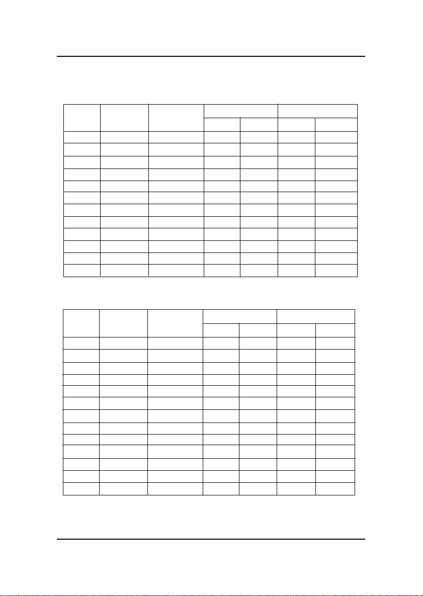
3. The DRAM addressing and the size supported by the mainboard is
shown next page.
4. Using 100MHz CPU Bus frequency, only PC100 DIMM is supported.
2-15
Page 16
CHAPTER 2 HARDWARE INST ALLA TION
Table 2.2-1 EDO DRAM Memory Addressing
DRAM
Tech.
DRAM
Density &
Width
DRAM
Addressing
Address Size
Row
Column
Single
Side(S)
MB/DIMM
no.
Double
pcs.
Side(D)
16M 1Mx16 SYMM 10 10 8MBx4 16MBx8
1Mx16 ASYM 12 8 8MBx4 16MBx8
2Mx8 ASYM 11 10 16MBx8 32MBx16
2Mx8 ASYM 12 9 16MBx8 32MBx16
4Mx4 SYMM 11 11 32MBx16 64MBx32
4Mx4 ASYM 12 10 32MBx16 64MBx32
64M 2Mx32 ASYM 11 10 16MBx2 32MBx4
2Mx32 ASYM 12 9 16MBx2 32MBx4
2Mx32 ASYM 13 8 16MBx2 32MBx4
4Mx16 SYMM 11 11 32MBx4 64MBx8
4Mx16 ASYM 12 10 32MBx4 64MBx8
8Mx8 ASYM 12 11 64MBx8128MBx16
Table 2.2-2 SDRAM Memory Addressing
DRAM
Tech.
DRAM
Density &
Width
DRAM
Addressing
Address Size
Row
Column
16M 1Mx16 ASYM 11 8 8MBx4 16MBx8
2Mx8 ASYM 11 9 16MBx8 32MBx16
4Mx4 ASYM 11 10 32MB 64MB
64M 2Mx32 ASYM 11 9 32MBx2 64MBx4
2Mx32 ASYM 12 8 16MBx2 32MBx4
4Mx16 ASYM 11 10 32MB 64MB
4Mx16 ASYM 13 8 32MB 64MB
8Mx8 ASYM 13 9 64MB 128MB
16Mx4 ASYM 13 10 128MB 256MB
64M 2Mx32 ASYM 11 8
4Mx16 ASYM 12 8
8Mx8 ASYM 12 9
16Mx4 ASYM 12 10
Single
Side(S)
MB/DIMM
no.
Double
pcs.
Side(D)
no.
pcs.
no.
pcs.
2-16
Page 17
CHAPTER 2 HARDWARE INST ALLA TION
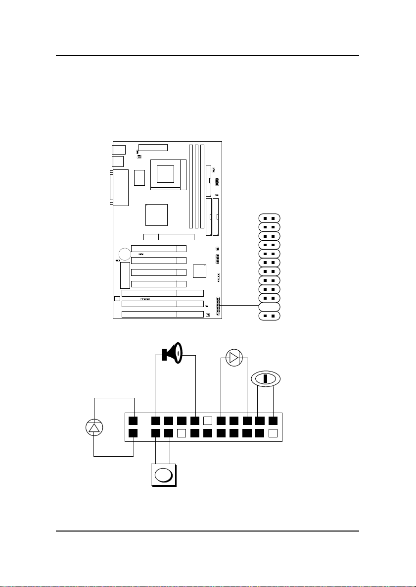
2.3 Case Connector: JFP
The Hardware Reset, Key Lock, Power LED, Speaker and HDD LED are
all grouped in JFP connector block for easy installation.
JFP
1
11
HDD LED
22
+
Speaker
10
x
x
20
Reset Switch
Figure 2.1
2-17
Power LED
+
10
22
Keylock
20
24
1
1124
Page 18

CHAPTER 2 HARDWARE INST ALLA TION
2.3-1 Hardware Reset
Reset switch is used to reboot the system rather than turning the power ON/
OFF. Avoid rebooting the system when the HDD LED is lit. You can
connect the Reset switch from the system case to this pin. (See Figure 2.1)
2.3-2 Keylock
Keylock allows you to disable the keyboard for security purposes. You can
connect the keylock to this pin. (See Figure 2.1)
2.3-3 Power LED
The Power LED is always lit while the system power is on. You can
connect the Power LED from the system case to this pin. (See Figure 2.1)
2.3-4 Speaker
Speaker from the system case is connected to this pin. (See Figure 2.1)
2.3-5 HDD LED
HDD LED shows the activity of a hard disk drive. Avoid turning the
power off while the HDD led is lit. You can connect the HDD LED from
the system case to this pin. (See Figure 2.1).
2-18
Page 19
CHAPTER 2 HARDWARE INST ALLA TION
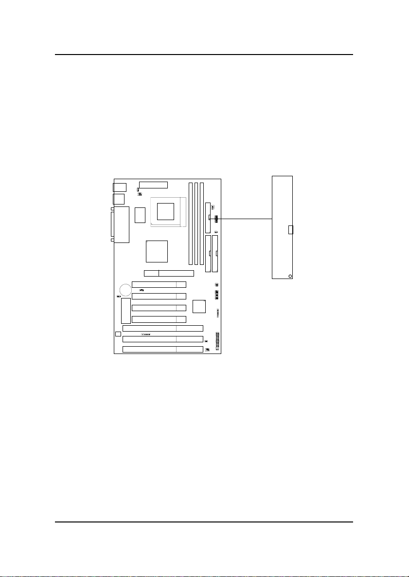
2.4 Floppy Disk Connector: FDC
The mainboard also provides a standard floppy disk connector, FDC that
supports 360K, 720K, 1.2M, 1.44M and 2.88M floppy disk types. Y ou can
attach a floppy disk cable directly to this connector.
FDC
1
2-19
Page 20
CHAPTER 2 HARDWARE INST ALLA TION
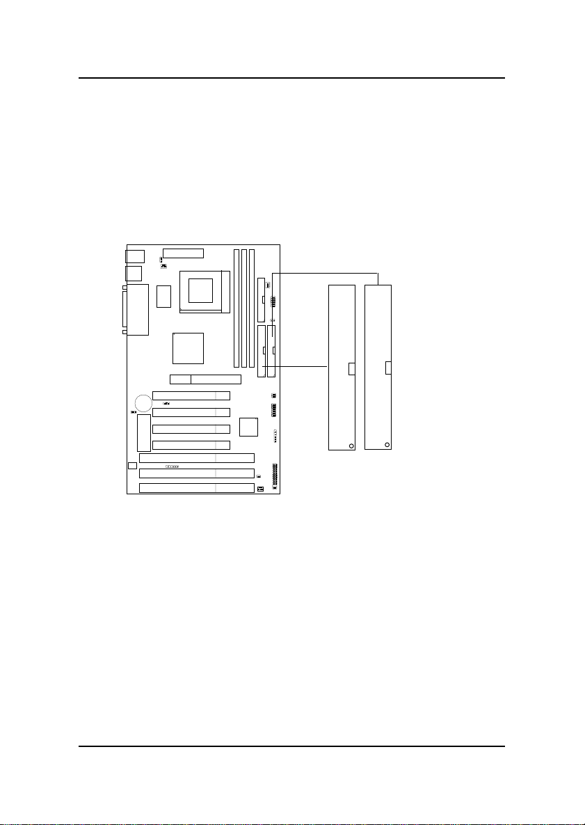
2.5 Hard Disk Connectors: IDE1 & IDE2
The mainboard has a 32-bit Enhanced PCI IDE Controller that provides
two HDD connectors IDE1 (Primary) and IDE2 (Secondary). You can
connect up to four hard disk drives, CD-ROM, 120MB Floppy and other
devices to IDE1 and IDE2.
Secondary IDE Connector
Primary IDE Connector
1
1
IDE1(Primary IDE Connector)
The first hard disk should always be connected to IDE1. IDE1
can connect a Master and a Slave drive.
IDE2(Secondary IDE Connector)
IDE2 can connect a Master and a Slave drive.
2-20
Page 21
CHAPTER 2 HARDWARE INST ALLA TION
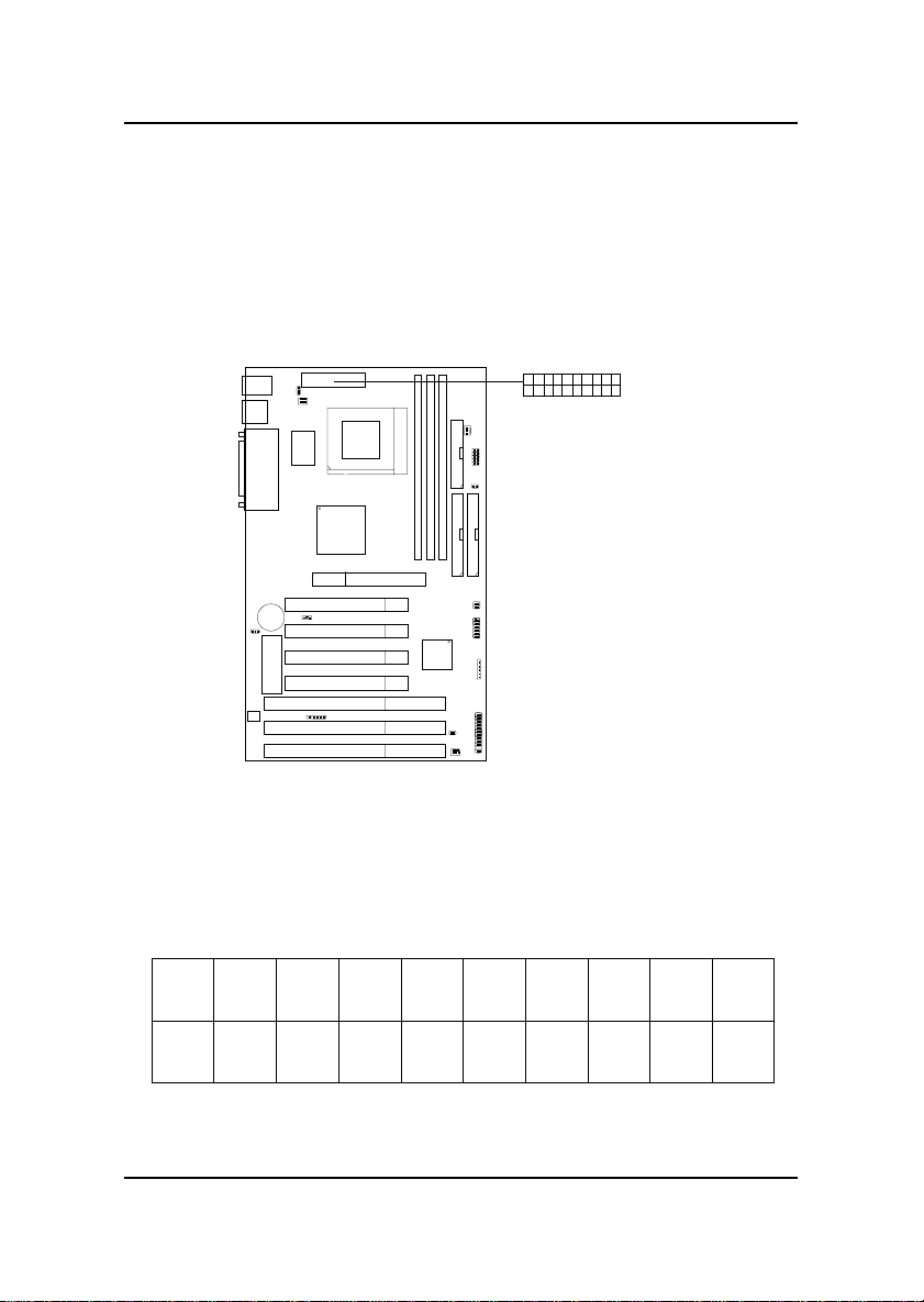
2.6 ATX 20-pin Power Connector: J1
This type of connector already supports the remote ON/OFF function.
However, you need to connect the Remote Power On/OFF switch (JRMS1/
JP1).
1
11
Power Connector
ATX Power Connector Pin Description
20
19
5V 5V -5V
18
17
GND GND
GND
141516
PS_ON
ATX
GND
13
10
20
12
11
3.3V-12V
12V
10
5V_SB
9
PW_OK
8
GND
GND
GND
6
7
5V5V
4
5
3
3.3V3.3V
2
1
2-21
Page 22
CHAPTER 2 HARDWARE INST ALLA TION
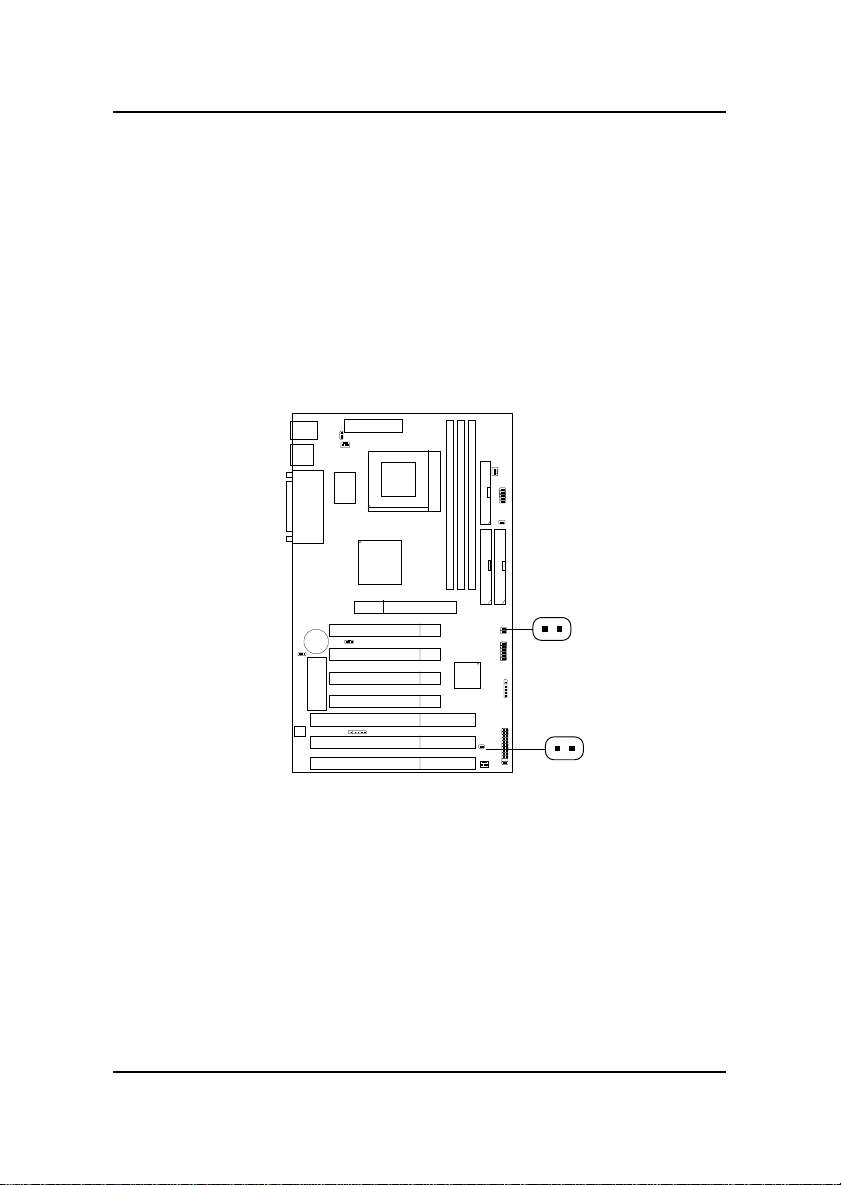
2.7 Remote Power On/Off Switches: JRMS1/
JRMS2 (JP1)
Connect to a 2-pin push button switch to JRMS1/JRMS2. Every time the
switch is shorted by pushing it once, the power supply will change its status
from OFF to ON. During ON stage: push once and the system goes to sleep
mode; push it more than 4 seconds will change its status from ON to OFF.
JRMS2 (JP1)
2-22
JRMS1
Page 23
CHAPTER 2 HARDWARE INST ALLA TION
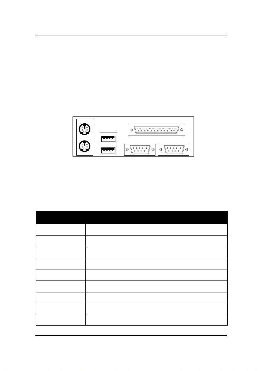
2.8 Serial Port Connectors: COM A & COM B
The mainboard has two serial ports COMA and COMB. These two ports
are 16550A high speed communication ports that send/receive 16 bytes
FIFOs. You can attach a mouse or a modem cable directly into these
connectors.
1 2 3 4 5
6 7 8 9
COM A
Serial Ports (9-pin Male)
COM B
PIN DEFINITION
Pin # Definition
1 DCD(Data Carry Detect)
2 SIN(Serial In or Receive Data)
3 SOUT(Serial Out or Transmit Data)
4 DTR(Data Terminal Ready)
5 GND
6 DSR(Data Set Ready)
7 RTS(Request To Send)
8 CTS(Clear To Send)
9 RI(Ring Indicate)
2-23
Page 24
CHAPTER 2 HARDWARE INST ALLA TION
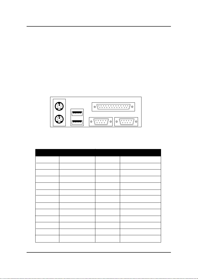
2.9 Parallel Port Connector: LPT
The mainboard provides a connector for LPT. A parallel port is a standard
printer port that also supports Enhanced Parallel Port(EPP) and Extended
capabilities Parallel Port(ECP).
Parallel Port (25-pin Female)
LPT
13
25
1
14
PIN DEFINITION
PIN # DEFINITION PIN # DEFINITION
1 STROBE 14 AUTO FEED#
2 DATA0 15 ERR#
3 DATA1 16 INIT#
4 DATA2 17 SLIN#
5 DATA3 18 GND
6 DATA4 19 GND
7 DATA5 20 GND
8 DATA6 21 GND
9 DATA7 22 GND
10 ACK# 23 GND
11 BUSY 24 GND
12 PE 25 GND
13 SELECT
2-24
Page 25
CHAPTER 2 HARDWARE INST ALLA TION
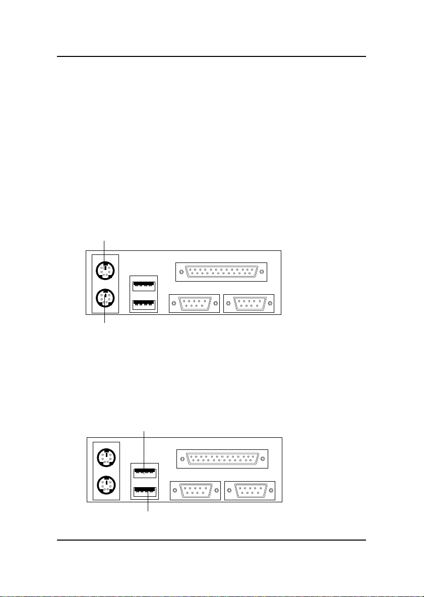
2.10 Keyboard Connector: PSKBC
Mouse Connector: PSMSC
The mainboard provides a standard PS/2® keyboard mini DIN connector for
attaching a keyboard. You can plug a keyboard cable directly to this
connector.
It also provides a standard PS/2® mouse mini DIN connector for attaching a
PS/2® mouse. You can plug a PS/2® mouse directly into this connector.
The connector location are shown below:
PS/2® Mouse (6-pin Female)
PS/2® Keyboard (6-pin Female)
2.11 USB Connectors: USB
The mainboard provide a USB(Universal Serial Bus) connector for
attaching USB devices like keyboard, mouse or etc. You can plug it directly
to this connector.
USB port 1
USB port 2
2-25
Page 26
CHAPTER 2 HARDWARE INST ALLA TION
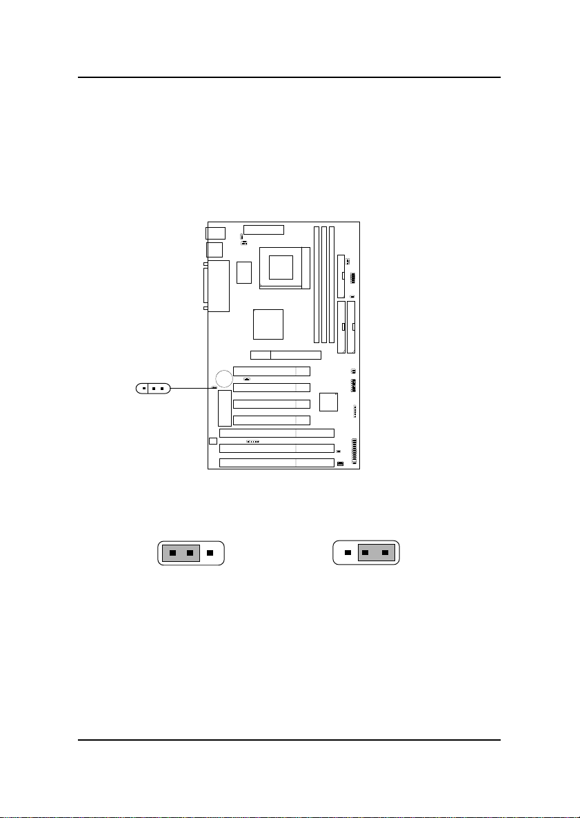
2.12 Clear CMOS Jumper: JP10
A battery must be used to retain the mainboard configuration in CMOS
RAM. Short 1-2 pins of JBAT1 to store the CMOS data.
3
1
JBAT1
1 133
22
Keep Data Clear Data
Note: You can clear CMOS by shorting 2-3 pin, while the system is of f.
Then, return to 1-2 pin position. A void clearing the CMOS while
the system is on, it will damage the mainboard. Always unplug
the power cord from the wall socket.
2-26
Page 27
CHAPTER 2 HARDWARE INST ALLA TION
2.13 Power On Mode Feature: JP11
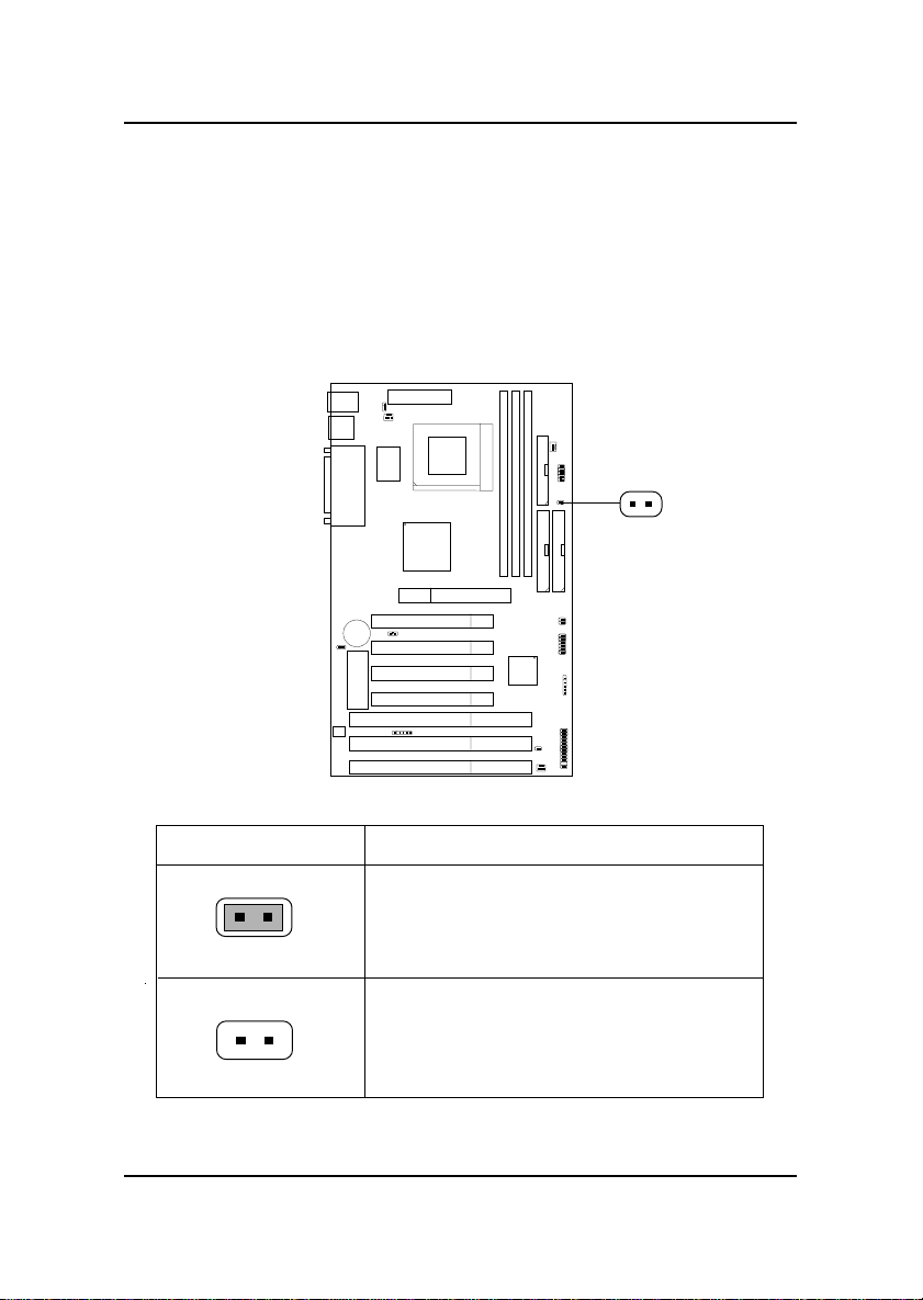
The mainboard supports two kinds of system boot up: the Boot-Up by
switch and the Immediate Boot-Up. With the Boot-Up by Switch, the
system will boot up only when the power on switch is pressed. For
Immediate Boot-Up, the system will boot up instantly when the power
connector is connected into the system.
JP11
Table 2.13: Power On Mode Feature
JP11
Feature
Select Immediate Boot-Up
Select Boot-Up by Switch
Note: Short JP11, when using Boot-Up by Switch feature. Open JP11, to enable
Immediate Boot-Up.
2-27
Page 28
CHAPTER 2 HARDWARE INST ALLA TION
2.14 Green Button and Power Switch: JP1
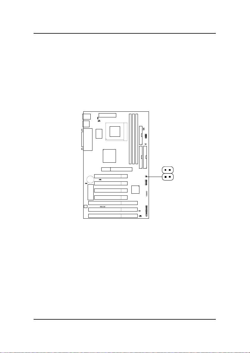
Attach a power saving switch to JP1(Green Button). When the switch is
pressed, the system immediately goes into suspend mode. Press any key
and the system wakes up.
JRMS2
Green Button
JP1
Note: The JP1(JRMS2) have the same function with JRMS1. (see Remote Power
On/Off switches: JRMS1/JRMS2)
2-28
Page 29
CHAPTER 2 HARDWARE INST ALLA TION
2.15 Wake-Up on LAN Connector: JWOL
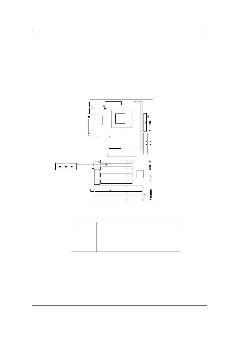
The JWOL connector is for use with LAN add-on cards that supports Wake
Up on LAN function. To use this function, you need to set the “Resume By
Ring” to enable at the BIOS Power Management Setup.
13
JWOL
PIN SIGNAL
1 5VSB
2 GND
3 MP_WAKEUP
Note: LAN wake-up signal is active “high”.
Note: To be able to use this function, you need a power supply that
provide enough power for this feature.
(750 ma power supply with 5V Stand-by)
2-29
Page 30
CHAPTER 2 HARDWARE INST ALLA TION
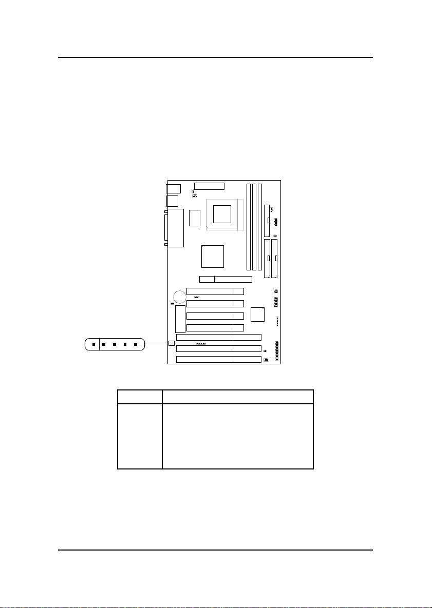
2.16 Modem Wake Up Connector: JMODEM
The JMODEM connector is for used with Modem add-on card that supports
the Modem Wake Up function. To use this function, you need to set the
“Resume By Ring” to enable at the BIOS Power Management Setup.
1
JMODEM
5
PIN SIGNAL
1NC
2 GND
3 MDM_WAKEUP
4NC
5 5VSB
Note: Modem wake-up signal is active “low”.
Note: To be able to use this function, you need a power supply that
provide enough power for this feature.
(750 ma power supply with 5V Stand-by)
2-30
Page 31
CHAPTER 2 HARDWARE INST ALLA TION
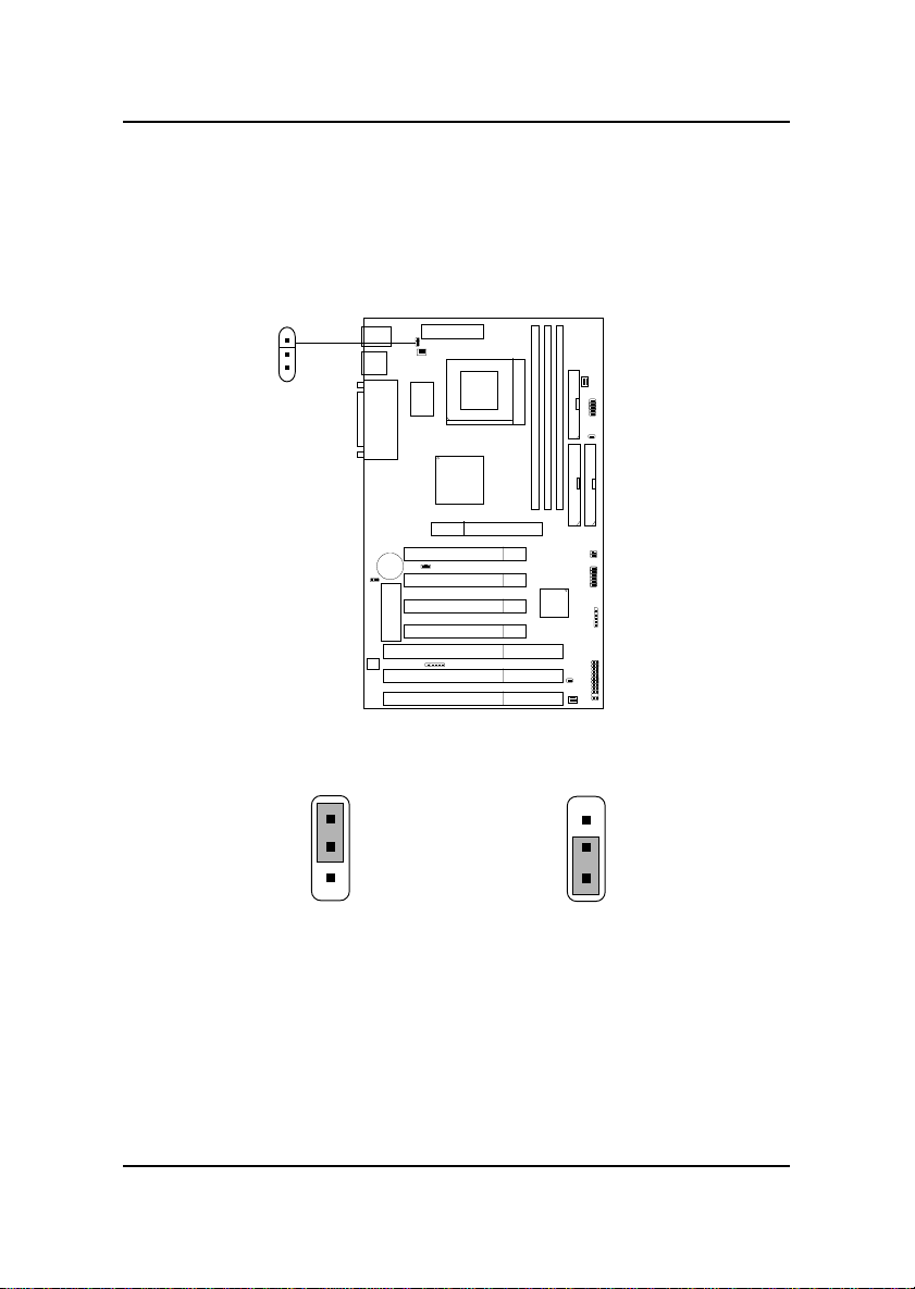
2.17 Keyboard Power: JP12
The JP12 jumper is for setting keyboard power on feature. The function
should be set in the BIOS keyboard W ake-up function.
1
3
JP12
1
3
5V (default)
Disable keyboard
power on function
1
3
5V Standby
Enable keyboard
power on function
Note: T o be able to use this function, you need a power supply that
provide enough power for this feature.
(750 ma power supply with 5V Stand-by)
2-31
Page 32
CHAPTER 2 HARDWARE INST ALLA TION
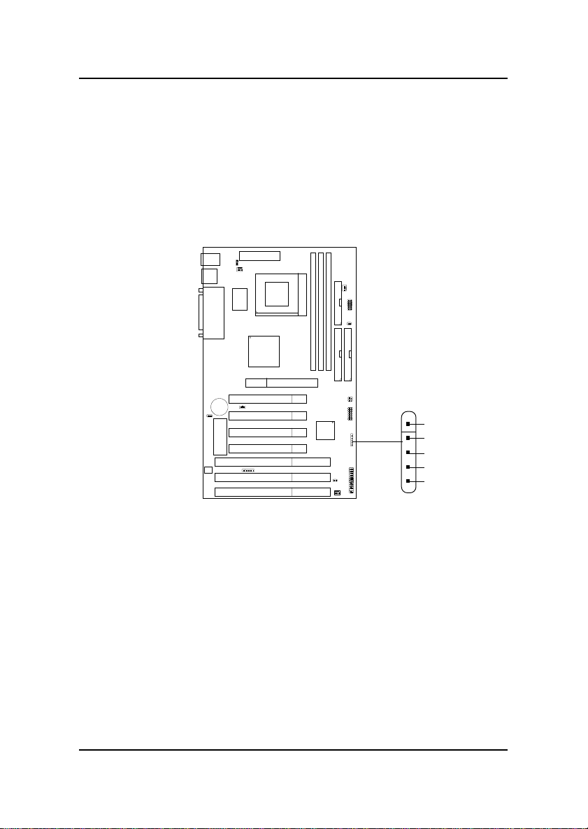
2.18 IrDA Infrared Module Connector: JP7
The mainboard provides one 5-pin infrared (IR) connector for IR modules.
This connector is for optional wireless transmitting and receiving infrared
module. You must configure the setting through the BIOS setup to use the
IR function. FIR and Consumer IR are reserved functions.
VCC
1
NC
IRRX
GND
IRTX
2-32
JP7
 Loading...