


CONTENTS
COMPONENT LOCATION DIAGRAM.................................A
TABLE OF CONTENT…………………………………………1
HOW TO USE THIS MANUAL………………………………. 2
INSIDE THE ATC-5250 MAINBOARD PACKAGE………... 3
CH
APTER 1 Introduction…………………………………...4
1-1 System Features..................................................................................4
1-2 Software Power Off Control..............................................................5
1-3 Wake-On-LAN……………………………………………………6
CHAPTER 2 Installation…………………………………….7
2-1 Installation Procedure …………………………………………....7
2-2 CPU Installation…………………………………………………. 8
2-2-1.A Intel Pentium CPU (P54C)………………………….… 11
2-2-1.B Intel Pentium MMXTM (P55C)…………………………. 13
2-2-1.C Cyrix 6x86MX CPU…………………………………….14
2-2-1.D Cyrix MII CPU…………………………………………. 16
2-2-1.E Cyrix 6x86L CPU………………………………………. 20
2-2-1.F AMD-K5 CPU………………………………………….. 21
2-2-1.G AMD-K6 & AMD-K6-2 CPU…………………………..22
2-2-1.H IDT Win Chip C6 CPU………………………………… 27
2-3 System Memory Installation……………………………………. 28
2-4 Connectors Description................................................................. 29
2-5 IDE Driver Installation.................................................................. 34
2-6 VIA MVP3 AGP VGA Driver Installation................................... 34
CHAPTER 3 Award BIOS Setup…………………………. 35
3-1 Update BIOS Procedure................................................................36
3-2 Award System BIOS Configuration Setup...................................37
Appendix A ……………………………………………………. 66
1

HOW TO USE THIS MANUAL
To obtain maximum use from this manual it is suggested:
Read Page A COMPONENT LOCATION DIAGRAM where you find the
mainboard layout diagram. Please refer to it when you configure the system.
Read about an overview of the mainboard features, packing contents, and how to
upgrade as well as to change hardware configurations such as memory size, CPU
type, jumper settings lists and connectors in the following categories:
INSIDE THE ATC-5250 MAINBOARD PACKAGE
Chapter 1 Introduction
Chapter 2 Installation
When you have finished reading of both chapter 1 and chapter 2, turn to Chapter 3
Award BIOS Setup where you will find the update BIOS procedure and the further
information which is stored in the SETUP is the system hardware configuration.
Your system dealer will set up the mainboard according to your demand of the
computer. It means that the current settings of your mainboard may not be the same as
the defaults shown in this user's manual. If you need to change your configuration,
please ask your dealer first. Be sure this will not void your system warranty, or ask
your dealer to do it for you.
REMARK
Intel® is a registered trademark of Intel Corporation.
All other brands and product names are trademarks registered trademarks of their respective companies.
2

INSIDE THE ATC-5250 MAINBOARD PACKAGE
The mainboard comes securely packed in a durable box or shipping carton. If any of
the following items are missing or damaged, please contact your supplier.
Each mainboard contains:
Q'TY Description
1 Mainboard : ATC-5250.
1 CD : Enhanced IDE driver
Award system BIOS Update Utility
VIA MVP3 AGP VGA Vgart.vxd
Utility
VIA IRQ Routing Utility
VIA MVP3 ACPI compliant utility
1 Cable : Enhanced IDE cable.
1 Cable : F.D.D. cable.
1 Cable : Serial & PS/2 mouse.
1 Cable : Serial / Parallel.
1 Manual : User manual. (English version)
3

CHAPTER 1 INTRODUCTION
ATC-5250 mainboard supports 100MHz host clock Super 7 processors, ie. AMD
K6-2, Cyrix M II. Of course , ATC-5250 mainboard also supports 66 ~ 95 MHz
host clock Socket 7 processors , ie. Intel Pentium & Pentium processor with
MMX technology , AMD K5/K6/K6-2 , Cyrix 6X86/6X86MX , and IDT Winchip.
ATC-5250 mainboard , VIA MVP3 chipset , supports AGP slot for best
performance of VGA display in 3D application .
1-1 SYSTEM FEATURES
Supports Intel Pentium (P54C) CPU operating from 100MHz to 200MHz, Intel
Pentium MMX
TM
166~233MHz (P55C), AMD K5, AMD K6, AMD K6-2, Cyrix
6x86MXTM, MII, 6x86L, IDT Win Chip C6 CPU.
VIA @ VT82C598MVP & VT82C586B (with keyboard control) chipset.
Uses three 168-pin DIMM sockets, provides three banks of 64-bit wide path up to
384MB SDRAM or 768 EDO DRAM (with parity chip ECC support).
Built-in Switching Voltage Regulator.(VRM 8.2 SPEC.)
Supports CPU core voltage range from 2.2V up to 3.5V.
Supports one AGP slot, three PCI slots with revision 2.1 interface compliant and
two 16-bit ISA slots.
Dual Master IDE connectors support Ultra DMA/33, up to four devices in two
channels for connecting of high capacity hard drive, CD-ROM, tape backup etc.
Two USB (Universal Serial Bus) headers support up to 127 devices.
AT style keyboard connector and PS/2 mouse header.
WINBOND W83877TF high-speed Super Multi-I/O chipset.
Supports Infrared transfer (IrDA TX/RX) connector.
One FDC port supports two devices.
Two 16550A fast UARTs compatible serial ports.
One EPP/ECP mode parallel printer port.
Supports AT & ATX power connectors.
Hardware Dimension is 220mm x 230mm (8.66" x 9.0"); BabyAT Form Factor.
4

1-2 SOFTWARE POWER OFF CONTROL
The mainboard design supports Software Power Off Control feature through the
SMM code in the BIOS under Windows 95/98, and MS-DOS operation system
environment. ( It needs to use with the ATX power supply.)
First, you should connect the power switch cable to the connector “PS-ON” on the
mainboard. In the BIOS screen of POWER MANAGEMENT SETUP’, choose “User
Defined” (or “Min. Power Saving” or “Max. Power Saving”) in ‘Power Manager’ and
choose “Yes” in ‘PM Control by APM’.
In Windows 95/98, if you would like to power off the system, you just choose
“shutdown the computer ?” in the “Shut Down Windows“ from Windows 95/98, then
the system power will be off directly and become the stand-by status. If you would
like to restart the system, just press the power switch button, and the system will be
powered on.
Note : If you will leave your system for several days, we suggest you use hardware
power off to shutdown your system.
5

1-3 Wake-On-LAN
The remote Wake-On-LAN mode of operation is a mechanism that uses
Advanced Micro Device Magic Packet technology to power up a sleeping workstation
on the network. This mechanism is accomplished when the LAN card receives a
specific packet of information, called a Magic Packet, addressed to the node on the
network. For additional protection, Secure ON is an optional security feature that can
be added to the Magic Packet that requires a password to power up the sleeping
workstation. When the LAN card is in remote Wake-On-LAN mode, main system
power can be shut down leaving power only for the LAN card and auxiliary power
recondition.
The LAN card performs no network activities while in the remote Wake-OnLAN mode of operation. It only monitors the network for receipt of a Magic Packet.
If a Magic Packet is addressed to the LAN card on the network, the LAN card wake
up the system. If the Secure ON feature has been enabled, the password added to the
Magic Packet is also verified prior to waking up the system.
CAUTION :
For Wake-on-LAN, the +5V standby for the power supply must be capable of
delivering +5V ±5% at 720mA. Failure to provide adequate standby current when
implementing Wake-on-LAN can damage the power supply. ( It needs to use with the
ATX power supply.)
Before you enable Wake-on-LAN function, please check your power supply
specification first to meet the above requirement or not.
6

CHAPTER 2 INSTALLATION
2-1 INSTALLATION PROCEDURE
Before installing the computer, please prepare all components such as CPU, DRAM;
peripherals such as hard drive, keyboard, CD-ROM and accessories such as cables.
Then, install the system as following:
1. Plug CPU, heat sink, cooling fan and DRAM modules into the ATC-5250
mainboard.
2. Set DIP switch based on your configuration.
3. Set jumpers based on your configuration.
4. Plug add-on cards into PCI/ISA slots, if needed.
5. Connect the power supply.
6. Connect I/O and other cables to the system.
7. Make sure all components and devices are well connected, turn on the power and
setup System BIOS based on your configuration.
8. Install peripheral devices, add-on card drivers and test them.
If all of above procedures are running successfully, turn it off and screw the chassis
cover to the system, and then connect external devices which are cabled to the system.
7

2-2 CPU INSTALLATION
ATC-5250 supports Pentium level CPUs.
For installation, please notice CPU pin 1 must align with the ZIF socket 7 pin 1
location. Before you install or upgrade your CPU, please read CPU guide from CPU
manufacturer to make sure the CPU voltage specification. Then choose the right
installation in section 2-2-1 based on your CPU type / brand and follow the
description to setup DIP Switch & Jumpers.
It is important to remember that you must set DIP switch of SW1, Jumpers of
JP1, JP2, JP3, JP4, JP5 accurately, so that you can power up your system
correctly.
The followings are the description of these important DIP switch & jumpers :
SW1,JP1,JP2,JP3 : The completed jumper group is to setup CPU and system
frequency.(with yellow color jumper cap)
JP4,JP5 : The completed jumper group is to setup CPU working
voltage.(with red color jumper cap)
The followings are the locations of these important DIP switches & Jumpers :
DIMM slots
JP4 JP1,JP2&JP3 SW1 JP5
(red color jumper cap) (yellow color (red color jumper cap)
jumper cap)
8

ATC-5250 uses the following DIP Switch & Jumpers to install the CPU easily.
SW1 (pin 1-3)for Frequency_Ratio and SW1(pin 4-6)for External Clock,
SW1(pin 7) & JP1 for CPU host clock/DRAM clock ratio selection, Asynchronous
or Synchronous .
JP2 & JP3 for CPU host clock/PCI clock ratio selection .
JP4 for different CPU voltage value.
JP5 for Single / Dual CPU Voltage selection.
The following DIP switches & Jumpers charts are the effective information for you to setup
correct CPU and total system speed , when installing your system with ATC-5250 mainboard :
SW1 setting
(The setting for CPU host clock and Times of multiple clock)
SW1 SW1-1 SW1-2 SW1-3 SW1 SW1-4 SW1-5 SW1-6
2.0X OFF OFF ON 66.6MHz ON ON OFF
2.5X OFF ON ON 75MHz OFF ON ON
3.0X OFF ON OFF 83.5MHz OFF ON OFF
1.5X;3.5X
OFF OFF OFF 95.25MHz OFF OFF ON
4.0X ON OFF ON 100MHz OFF OFF OFF
4.5X ON ON ON
5.0X ON ON OFF
5.5X ON OFF OFF
SW1(pin7) & JP1 setting
(The setting for Asynchronous and Synchronous mode)
DRAM CLK. SW1-7 JP1
ASYNC ON Pin 1-2
SYNC OFF Pin 2-3
* ASYNC. mode: The speed of the DRAM clock is not the same as the CPU host clock, ie.
When the CPU host clock is 100 MHz , and the DRAM clock is 66 MHz .
** SYNC. Mode: The speed of the DRAM clock is the same as the CPU host clock, ie.
1. When the CPU host clock is 100 MHz , and the
SDRAM clock follows PC-100 specification (100MHz) .
2. When the CPU host clock is 66 ~ 83.3 MHz , and
the DRAM/SDRAM clock is not PC-100 spec.(lower than 100MHz).
how to set up DIP switch:
ON DIP
1 2 3 4 5 6 7 SW1
DIP switch, (i.e. : OFF, OFF, OFF, ON,
ON, OFF, OFF)
ON : switch to the ‘ON’ position.
OFF : switch to the ‘OFF’ position.
9

JP2 & JP3 Setting
(The setting for frequency-ratio comparing with the PCI clock and the CPU host clock.)
CPU_CLK JP 2 JP 3
66.6MHz Pin 2-3 Pin 2-3
75MHz Pin 1-2 Pin 1-2
83.3MHz Pin 1-2 Pin 1-2
95.25MHz Pin 1-2 Pin 2-3
100MHz Pin 1-2 Pin 2-3
JP4 Setting
(The setting for CPU core voltage selection)
Vcore Pin1 & Pin5 Pin2 & Pin6 Pin3 & Pin7 Pin4 & Pin8
2.2V OPEN CLOSE OPEN OPEN
2.7V CLOSE CLOSE CLOSE OPEN
2.8V OPEN OPEN OPEN CLOSE
2.9V CLOSE OPEN OPEN CLOSE
3.2V OPEN OPEN CLOSE CLOSE
3.3V CLOSE OPEN CLOSE CLOSE
3.5V CLOSE CLOSE CLOSE CLOSE
JP5 setting
(The setting for Single/Dual Voltage supporting for Pentium level Processor)
Mode JP5 (Pin1-2,3-4,5-6)
Single Voltage Mode(Vcore = Vi/o)*
OPEN
Dual Voltage Mode(Vcore ≠Vi/o)**
CLOSE
* P54C mode (Single Voltage Mode) : supports for Intel Pentium, AMD-
K5,Cyrix 6X86, IDT Win Chip C6.
** P55C mode (Dual Voltage Mode) : supports for Intel Pentium MMX,
AMD-K6, AMD-K6-2, Cyrix 6X86L,
Cyrix 6X86MX, Cyrix M II.
how to set up jumpers:
OPEN CLOSE
( remove the ( put on the
Pin1-2 Pin2-3
jumper cap) jumper cap)
1 2 3
1 2 3
10

2-2-1 CPU TYPE SELECTION
A. INTEL PENTIUM CPU
(P54C)
※ P54C VRE : 3.400V~3.600V
(The fourth line of the mark on the under-side
of the processor contains a code that identifies the voltage level
type. V is VRE, S is standard. )
JP4(3.5V)
JP4
Pin1 & Pin5 Pin2 & Pin6 Pin3 & Pin7 Pin4 & Pin8
Vcore CLOSE CLOSE CLOSE CLOSE
※ P54C STD : 3.135V ~ 3.600V
(The fourth line of the mark on the
under-side of the processor contains a code that identifies
the voltage level type. V is VRE, S is standard. )
JP4 (3.3V)
JP4
Pin1 & Pin5 Pin2 & Pin6 Pin3 & Pin7 Pin4 & Pin8
Vcore CLOSE OPEN CLOSE CLOSE
JP5 Setting (Single)
Mode JP5 (Pin1-2, 3-4, 5-6)
Single Voltage Mode(Vcore = Vi/o)*
OPEN
JP1, JP2 & JP3 Settings
CPU host clock/DRAM/PCI clock JP 1 JP 2 JP3
66MHz/66MHz/33MHz Pin 2-3 Pin 2-3 Pin 2-3
A-1. Intel Pentium 100MHz
INTERNAL CPU
CLOCK
SW1 Ext.x Frq.
100MHz ON
OFF
1 2 3 4 5 6 7
66 x 1.5
11

A-2. Intel Pentium 133MHz
INTERNAL CPU
CLOCK
SW1 Ext.x Frq.
133MHz
ON
OFF
1 2 3 4 5 6 7
66 x 2.0
A-3. Intel Pentium 166MHz
INTERNAL CPU
CLOCK
SW1 Ext.x Frq.
166MHz ON
OFF
1 2 3 4 5 6 7
66 x 2.5
A-4. Intel Pentium 200MHz
INTERNAL CPU
CLOCK
SW1 Ext.x Frq.
200MHz ON
OFF
1 2 3 4 5 6 7
66 x 3.0
12

B. INTEL PENTIUM MMXTM CPU (P55C)
JP4 (2.8V)
JP4
Pin1 & Pin5 Pin2 & Pin6 Pin3 & Pin7 Pin4 & Pin8
Vcore OPEN OPEN OPEN CLOSE
JP5 Setting (Dual)
Mode JP5 (Pin1-2, 3-4, 5-6)
Dual Voltage Mode(Vcore ≠Vi/o)**
CLOSE
JP1, JP2 & JP3 S
ettings
CPU host clock/DRAM/PCI clock JP1 JP2 JP3 66MHz/66MHz/33MHz Pin 2-3 Pin 2-3 Pin 2-3
B-1. Intel Pentium MMXTM 166MHz
INTERNAL CPU
CLOCK
SW1 Ext.x Frq.
166MHz
ON
OFF
1 2 3 4 5 6 7
66 x 2.5
B-2. Intel Pentium MMXTM 200MHz
INTERNAL CPU
CLOCK
SW1 Ext.x Frq.
200MHz ON
OFF
1 2 3 4 5 6 7
66 x 3.0
B-3. Intel Pentium MMXTM 233MHz
INTERNAL CPU
CLOCK
SW1 Ext.x Frq.
233MHz ON
OFF
1 2 3 4 5 6 7
66 x 3.5
13

C. Cyrix 6x86MX CPU
JP4 (2.9V)
JP4
Pin1 & Pin5 Pin2 & Pin6 Pin3 & Pin7 Pin4 & Pin8
Vcore CLOSE OPEN OPEN CLOSE
JP5 Setting (Dual)
Mode JP5 (Pin1-2, 3-4, 5-6)
Dual Voltage Mode(Vcore ≠Vi/o)**
CLOSE
JP1, JP2 & JP3 Settings
CPU host clock/DRAM/PCI clock JP1 JP2 JP3 66MHz/66MHz/33MHz Pin 2-3 Pin 2-3 Pin 2-3
C-1. Cyrix 6x86MX PR166 @ 66MHz Bus 2x
INTERNAL CPU
CLOCK
SW1
Ext.x Frq.
PR166 ON
OFF
1 2 3 4 5 6 7
66 x 2.0
C-2. Cyrix 6x86MX PR200 @ 66MHz Bus 2.5x
INTERNAL CPU
CLOCK
SW1
Ext.x Frq.
PR200 ON
OFF
1 2 3 4 5 6 7
66 x 2.5
C-3. Cyrix 6x86MX PR233 @ 66MHz Bus 3x
INTERNAL CPU
CLOCK
SW1
Ext.x Frq.
PR233 ON
OFF
1 2 3 4 5 6 7
66 x 3.0
C-4. Cyrix 6x86MX PR233 @ 75MHz Bus 2.5x
14

JP4 (2.9V)
JP4
Pin1 & Pin5 Pin2 & Pin6 Pin3 & Pin7 Pin4 & Pin8
Vcore CLOSE OPEN OPEN CLOSE
JP5 Setting (Dual)
Mode JP5 (Pin1-2, 3-4, 5-6)
Dual Voltage Mode(Vcore ≠Vi/o)**
CLOSE
JP1, JP2 & JP3 Settings
CPU host clock/DRAM/PCI clock JP1 JP2 JP3 75MHz/75MHz/30MHz Pin 2-3 Pin 1-2 Pin 1-2
INTERNAL CPU
CLOCK
SW1
Ext.x Frq.
PR233 ON
OFF
1 2 3 4 5 6 7
75 x 2.5
15

D. Cyrix MII CPU
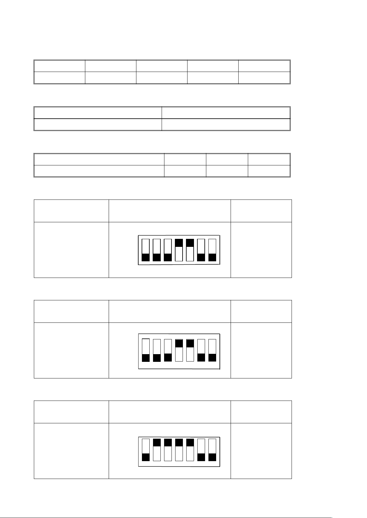
D-1 Cyrix MII 300MHz @ 66MHz Bus 3.5x
JP4(2.9V)
JP4
Pin1 & Pin5 Pin2 & Pin6 Pin3 & Pin7 Pin4 & Pin8
Vcore CLOSE OPEN OPEN CLOSE
JP5 Setting (Dual)
Mode JP5 (Pin1-2, 3-4, 5-6)
Dual Voltage Mode(Vcore ≠Vi/o)**
CLOSE
JP1, JP2 & JP3 Settings
CPU host clock/DRAM/PCI clock JP1 JP2 JP3
66MHz/66MHz/33MHz Pin 2-3 Pin 2-3 Pin 2-3
INTERNAL CPU
CLOCK
SW1 Ext.x Frq.
MII 300MHz ON
OFF
1 2 3 4 5 6 7
66 x 3.5
D-2 Cyrix MII 300MHz @ 75MHz Bus 3x
JP4(2.9V)
JP4
Pin1 & Pin5 Pin2 & Pin6 Pin3 & Pin7 Pin4 & Pin8
Vcore CLOSE OPEN OPEN CLOSE
JP5 Setting (Dual)
Mode JP5 (Pin1-2, 3-4, 5-6)
Dual Voltage Mode(Vcore ≠Vi/o)**
CLOSE
16

JP1, JP2 &
JP3 Settings
CPU host clock/DRAM/PCI clock JP1 JP2 JP3
75MHz/75MHz/30MHz Pin 2-3 Pin 1-2 Pin 1-2
INTERNAL CPU
CLOCK
SW1 Ext.x Frq.
MII 300MHz ON
OFF
1 2 3 4 5 6 7
75 x 3.0
D-3 Cyrix MII 333MHz @ 83MHz Bus 2.5x
JP4(2.9V)
JP4
Pin1 & Pin5 Pin2 & Pin6 Pin3 & Pin7 Pin4 & Pin8
Vcore CLOSE OPEN OPEN CLOSE
JP5 Setting (Dual)
Mode JP5 (Pin1-2, 3-4, 5-6)
Dual Voltage Mode(Vcore ≠Vi/o)**
CLOSE
JP1, JP2 & JP 3 Settings
CPU host clock/DRAM/PCI clock JP1 JP2 JP3
83.3MHz/83.3MHz/33MHz Pin 2-3 Pin 1-2 Pin 1-2
INTERNAL CPU
CLOCK
SW1 Ext.x Frq.
MII 333MHz ON
OFF
1 2 3 4 5 6 7
83 x 2.5
17

D-4 Cyrix MII 333MHz @ 100MHz Bus 2.5x
JP4(2.2V)
JP4
Pin1 & Pin5 Pin2 & Pin6 Pin3 & Pin7 Pin4 & Pin8
Vcore OPEN CLOSE OPEN OPEN
JP5 Setting (Dual)
Mode JP5 (Pin1-2, 3-4, 5-6)
Dual Voltage Mode(Vcore ≠Vi/o)**
CLOSE
SW1(
Pin7), JP1, JP2 & JP3 Settings
CPU host clock/DRAM/PCI clock SW1-Pin7 JP1 JP2 JP3 100MHz/100MHz/33MHz* OFF Pin 2-3 Pin 1-2 Pin 2-3 100MHz/66MHz/33MHz** ON Pin 1-2 Pin 1-2 Pin 2-3
* Please use for PC-100 SDRAM module (SYNC.)
** Please use non PC-100 SDRAM module or EDO DIMM module (ASYNC.)
INTERNAL CPU
CLOCK
SW1 Ext.x Frq.
MII 333MHz ON
OFF
1 2 3 4 5 6 7
100 x 2.5
18

D-5 Cyrix MII 350MHz @ 100MHz Bus 3x
JP4(2.2V)
JP4
Pin1 & Pin5 Pin2 & Pin6 Pin3 & Pin7 Pin4 & Pin8
Vcore OPEN CLOSE OPEN OPEN
JP5 Setting (Dual)
Mode JP5 (Pin1-2, 3-4, 5-6)
Dual Voltage Mode(Vcore ≠Vi/o)**
CLOSE
SW1(Pin7), JP1, JP2 & JP3 Settings
CPU host clock/DRAM/PCI clock SW1-pin7 JP1 JP2 JP3 100MHz/100MHz/33MHz* OFF Pin 2-3 Pin 1-2 Pin 2-3 100MHz/66MHz/33MHz** ON Pin 1-2 Pin 1-2 Pin 2-3
* Please use for PC-100 SDRAM module (SYNC.)
** Please use non PC-100 SDRAM module or EDO DIMM module (ASYNC.)
INTERNAL CPU
CLOCK
SW1 Ext.x Frq.
MII 350MHz ON
OFF
1 2 3 4 5 6 7
100 x 3.0
19

E. Cyrix 6x86L CPU (dual voltage)
JP4 (2.8V)
JP4
Pin1 & Pin5 Pin2 & Pin6 Pin3 & Pin7 Pin4 & Pin8
Vcore OPEN OPEN OPEN CLOSE
JP5 Setting (Dual)
Mode JP5 (Pin1-2, 3-4, 5-6)
Dual Voltage Mode(Vcore ≠Vi/o)**
CLOSE
JP1, JP2 & JP3 Settings
CPU host clock/DRAM/PCI clock JP1 JP2 JP3 66MHz/66MHz/33MHz* Pin 2-3 Pin 2-3 Pin 2-3
Cyrix 6x86L PR166+
INTERNAL CPU
CLOCK
SW1
Ext.x Frq.
PR166+ ON
OFF
1 2 3 4 5 6 7
66 x 2.0
20
F. AMD-K5 CPU Series
JP4(3.5V)
JP4
Pin1 & Pin5 Pin2 & Pin6 Pin3 & Pin7 Pin4 & Pin8
Vcore CLOSE CLOSE CLOSE CLOSE
JP5 Setting (Single)
Mode JP5 (Pin1-2, 3-4, 5-6)
Single Voltage Mode(Vcore = Vi/o)*
OPEN
JP1, JP2 & JP3 Settings
CPU host clock/DRAM/PCI clock JP1 JP2 JP3 66MHz/66MHz/33MHz* Pin 2-3 Pin 2-3 Pin 2-3
F-1. AMD-K5 PR100
INTERNAL CPU
CLOCK
SW1
Ext.x Frq.
PR100
ON
OFF
1 2 3 4 5 6 7
66 x 1.5
F-2. AMD-K5 PR133
INTERNAL CPU
CLOCK
SW1
Ext.x Frq.
PR133 ON
OFF
1 2 3 4 5 6 7
66 x 1.5
F-3. AMD-K5 PR166
INTERNAL CPU
CLOCK
SW1
Ext.x Frq.
PR166 ON
OFF
1 2 3 4 5 6 7
66 x 2.5
21

G. AMD-K6 CPU
JP1, JP2 & JP3 Settings
CPU host clock/DRAM/PCI clock JP1 JP2 JP3 66MHz/66MHz/33MHz Pin 2-3 Pin 2-3 Pin 2-3
JP5 Setting (Dual)
Mode JP5 (Pin1-2, 3-4, 5-6)
Dual Voltage Mode(Vcore ≠Vi/o)**
CLOSE
G-1. AMD-K6 166MHz
JP4(2.9V)
JP4
Pin1 & Pin5 Pin2 & Pin6 Pin3 & Pin7 Pin4 & Pin8
Vcore CLOSE OPEN OPEN CLOSE
INTERNAL CPU
CLOCK
SW1
Ext.x Frq.
166MHz
ON
OFF
1 2 3 4 5 6 7
66 x 2.5
G-2. AMD-K6 200MHz
JP4(2.9V)
JP4
Pin1 & Pin5 Pin2 & Pin6 Pin3 & Pin7 Pin4 & Pin8
Vcore CLOSE OPEN OPEN CLOSE
INTERNAL CPU
CLOCK
SW1
Ext.x Frq.
200MHz
ON
OFF
1 2 3 4 5 6 7
66 x 3.0
22

G-3a. AMD-K6 233MHz
JP4(3.2V)
JP4
Pin1 & Pin5 Pin2 & Pin6 Pin3 & Pin7 Pin4 & Pin8
Vcore OPEN OPEN CLOSE CLOSE
INTERNAL CPU
CLOCK
SW1
Ext.x Frq.
233MHz
ON
OFF
1 2 3 4 5 6 7
66 x 3.5
G-3b. AMD-K6-2 233MHz
JP4(2.2V)
JP4
Pin1 & Pin5 Pin2 & Pin6 Pin3 & Pin7 Pin4 & Pin8
Vcore OPEN CLOSE OPEN OPEN
INTERNAL CPU
CLOCK
SW1
Ext.x Frq.
233MHz
ON
OFF
1 2 3 4 5 6 7
66 x 3.5
G-4a. AMD-K6 266 MHz
JP4(2.2V)
JP4
Pin1 & Pin5 Pin2 & Pin6 Pin3 & Pin7 Pin4 & Pin8
Vcore OPEN CLOSE OPEN OPEN
INTERNAL CPU
CLOCK
SW1
Ext.x Frq.
266MHz
ON
OFF
1 2 3 4 5 6 7
66 x 4.0
23

G-4b. AMD-K6-2 266 MHz
JP4(2.2V)
JP4
Pin1 & Pin5 Pin2 & Pin6 Pin3 & Pin7 Pin4 & Pin8
Vcore OPEN CLOSE OPEN OPEN
INTERNAL CPU
CLOCK
SW1
Ext.x Frq.
266MHz
ON
OFF
1 2 3 4 5 6 7
66 x 4.0
G-5a. AMD-K6 300MHz
JP4(2.2V)
JP4
Pin1 & Pin5 Pin2 & Pin6 Pin3 & Pin7 Pin4 & Pin8
Vcore OPEN CLOSE OPEN OPEN
JP5 Setting (Dual)
Mode JP5 (Pin1-2, 3-4, 5-6)
Dual Voltage Mode(Vcore ≠Vi/o)**
CLOSE
JP1, JP2 & JP3 Settings
CPU host clock/DRAM/PCI clock JP1 JP2 JP3 66MHz/66MHz/33MHz Pin 2-3 Pin 2-3 Pin 2-3
INTERNAL CPU
CLOCK
SW1 Ext.x Frq.
300MHz ON
OFF
1 2 3 4 5 6 7
66 x 4.5
24

G-5b. AMD-K6-2 300MHz
JP4(2.2V)
JP4
Pin1 & Pin5 Pin2 & Pin6 Pin3 & Pin7 Pin4 & Pin8
Vcore OPEN CLOSE OPEN OPEN
JP5 Setting (Dual)
Mode JP5 (Pin1-2, 3-4, 5-6)
Dual Voltage Mode(Vcore ≠Vi/o)
CLOSE
SW1(Pin7), JP1, JP2 & JP3 Settings
CPU host clock/DRAM/PCI clock SW1-pin7 JP1 JP2 JP3 100MHz/100MHz/33MHz* OFF Pin 2-3 Pin 1-2 Pin 2-3 100MHz/66MHz/33MHz** ON Pin 1-2 Pin 1-2 Pin 2-3
* Please use for PC-100 SDRAM module (SYNC.)
** Please use non PC-100 SDRAM module or EDO DIMM module (ASYNC.)
INTERNAL CPU
CLOCK
SW1 Ext.x Frq.
300MHz ON
OFF
1 2 3 4 5 6 7
100 x 3.0
G-5c. AMD-K6-2 333MHz
JP4(2.2V)
JP4
Pin1 & Pin5 Pin2 & Pin6 Pin3 & Pin7 Pin4 & Pin8
Vcore OPEN CLOSE OPEN OPEN
JP5 Setting (Dual)
Mode JP5 (Pin1-2, 3-4, 5-6)
Dual Voltage Mode(Vcore ≠Vi/o)
CLOSE
25

SW1(Pin7), JP1, JP2 & JP3 Settings
CPU host clock/DRAM/PCI clock SW1-pin7 JP1 JP2 JP3 95MHz/95MHz/33MHz* OFF Pin 2-3 Pin 1-2 Pin 2-3 95MHz/66MHz/33MHz** ON Pin 1-2 Pin 1-2 Pin 2-3
* Please use for PC-100 SDRAM module (SYNC.)
** Please use non PC-100 SDRAM module or EDO DIMM module (ASYNC.)
INTERNAL CPU
CLOCK
SW1 Ext.x Frq.
333MHz ON
OFF
1 2 3 4 5 6 7
95 x 3.5
G-6. AMD-K6-2 350MHz
JP4(2.2V)
JP4
Pin1 & Pin5 Pin2 & Pin6 Pin3 & Pin7 Pin4 & Pin8
Vcore OPEN CLOSE OPEN OPEN
JP5 Setting (Dual)
Mode JP5 (Pin1-2, 3-4, 5-6)
Dual Voltage Mode(Vcore ≠Vi/o)**
CLOSE
SW1(Pin7), JP1 & JP2 Settings
CPU host clock/DRAM/PCI clock SW1-pin7 JP1 JP2 JP3 100MHz/100MHz/33MHz* OFF Pin 2-3 Pin 1-2 Pin 2-3 100MHz/66MHz/33MHz** ON Pin 1-2 Pin 1-2 Pin 2-3
* Please use for PC-100 SDRAM module (SYNC.)
** Please use non PC-100 SDRAM module or EDO DIMM module (ASYNC.)
INTERNAL CPU
CLOCK
SW1 Ext.x Frq.
350MHz ON
OFF
1 2 3 4 5 6 7
100 x 3.5
26

H. IDT Win Chip C6
JP4(3.5V)
JP4
Pin1 & Pin5 Pin2 & Pin6 Pin3 & Pin7 Pin4 & Pin8
Vcore CLOSE CLOSE CLOSE CLOSE
JP5 Setting (Single)
Mode JP5 (Pin1-2, 3-4, 5-6)
Single Voltage Mode(Vcore = Vi/o)*
OPEN
H-1. IDT Win Chip C6 200MHz
JP1, JP2 & JP3 Settings
CPU host clock/DRAM/PCI clock JP1 JP2 JP3 66MHz/66MHz/33MHz Pin 2-3 Pin 2-3 Pin 2-3
INTERNAL CPU
CLOCK
SW1 Ext.x Frq.
200MHz ON
OFF
1 2 3 4 5 6 7
66 x 3.0
H-2 IDT Win Chip C6 225MHz
JP1, JP2 & JP3 Settings
CPU host clock/DRAM/PCI clock JP1 JP2 JP3 75MHz/75MHz/30MHz Pin 2-3 Pin 1-2 Pin 1-2
INTERNAL CPU
CLOCK
SW1 Ext.x Frq.
225MHz ON
OFF
1 2 3 4 5 6 7
75 x 3.0
27

2-3 SYSTEM MEMORY INSTALLATION
The ATC-5250 provides three 168-pin DIMM sockets for system memory
expansion from 8MB to 768MB. These three DIMMs are arranged to three banks,
please refer to page A. Each bank provides 64-bit wide data path.
※ Samples of System Memory Combinations Options ※
BANK0 BANK1 BANK2 Total Memory
DIMM 1 DIMM 2 DIMM 3 DIMM 1-3
32MBx1 - - 32MB
- - 32MBx1 32MB
8MBx1 16MBx1 16MBx1 40MB
32MBx1 32MBx1 - 64MB
- 32MBx1 32MBx1 64MB
64MBx1 - - 64MB
: : : :
- 64MBx1 64MBx1 128MB
128MBx1 - - 128MB
- 128MBx1 - 128MB
- - 128MBx1 128MB
128MBx1 128MBx1 - 256MB
128MBx1 - 128MBx1 256MB
- 128MBx1 128MBx1 256MB
256MBx1 - - 256MB
: : : :
256MBx1 256MBx1 - 512MB
256MBx1 - 256MBx1 512MB
- 256MBx1 256MBx1 512MB
256MBx1 256MBx1 256MBx1 768MB
28

2-4 CONNECTORS DESCRIPTION
The locations of following connectors are indicated in page A. When you plug
wires into the following connector of CONN1, you should have the pin 1 edge of the
wires align with the pin 1 end of the connector.
CONN1 : speaker, keyboard lock, reset, SMI,
turbo LED, and IDE LED connectors.
Socket 7
TB-LED : Turbo LED indicator, LED on
when system runs higher speed.
GND
+5V
+ +
RST SMI TB-LED IDE-LED
PS ON
SPK PWR LED K-LOCK
SPK : speaker
Speaker
GND
GND
VCC
Power LED connector
Power LED +
N/C
GND (power)
Keylock
GND
RST : Reset connector
Reset Signal
GND
SMI : SMI lead
GND
SMI Signal
29

Pin 12 PS_ON : Power Button
Pin 24 Pin 12 : PS_ON Pin 24 : +5VSB
CPU FAN1 : CPU cooling fan connector. Wire
with +12V voltage (most likely red wire) must
be plugged into pin2, and GROUND wires
(most likely black wire) must be plugged into
pin1. Please confirm the wire color
re-presentation with your supplier.
CAUTION: Plug the wire into wrong connector will
DAMAGE fan and mainboard.
3 2 1
GND +12V GND
IR1 : Infrared module connector.
Socket 7
IDE-LED : IDE devices indicator LED
connector. IDE-LED stays ON indicates
LED signal on-board IDE devices in operation. The
+5V red wire of the HDD connector must be
connected to the pin which is +5V.
SOCKET 7
FAN 1
1 +5V
2 FIRRX
3 IRRX
4 GND
5 IRTX
30

PW1 : ATX mode +3.3/5/12V power supply connector.
1 10
11 20
PW2 : AT mode +5V voltage power supply connector.
SOCKET 7
COM1/COM2 : these two connectors are used
to connect serial port cables.
pin signal name
1 NDCDA/B
2 NSINA/B
3 NSOUTA/B
4 NDTRA/B
5 GND
6 NDSRA/B
7 NRTSA/B
8 NCTSA/B
9 NRIA/B
A is COM1, B is COM2
KB: 5-pin AT style keyboard connector.
PS/2 Mouse: It is used to connect an optional cable.
pin1: data
pn2: N/C
pin3: GND
pin4: VCC
pin5: clock
pin6: N/C
1 3.3V 6 +5V 11 3.3V 16 GND
2 3.3V 7 GND 12 -12V 17 GND
3 GND 8 PWRGD 13 GND 18 -5V
4 +5V 9 5VSB 14*PS_ON 19 +5V
5 GND 10 +12V 15 GND 20 +5V
6 7 8 9
1 2 3 4 5
3 1 2 4
5 6
31

FDC1 : this connector is used to connect the floppy
drive through a cable.
pin signal pin signal
2 RWC- 20 STEP4 Reserved 22 Write Data
6 FDEDIN 24 Write Gate
8 Index- 26 Track 00-
0 Motor EnableA- 28 Write Protect12 Drive Sele.B- 30 Read Data14 Drive Sele.A- 32 Side 1 Sele.16 Motor EnableB- 34 DisketteChange
18 DIR-
All of odd pins are ground
LPT : this connector is used to connect parallel
port cable.
pin signal pin signal
1 STROBE- 10 ACK2 Data Bit 0 11 BUSY
3 Data Bit 1 12 PE
4 Data Bit 2 13 SLCT
5 Data Bit 3 14 Auto Feed6 Data Bit 4 15 ERROR-
Data Bit 5 16 INIT8 Data Bit 6 17 SLCT IN9 Data Bit 7
pin18 -- pin25 are GND
14 1
34 33
2 1
26 13
32

IDE1/IDE2 : these two connectors are used to connect IDE
devices through IDE cables, a total of 4 devices
can be connected.
pin signal pin signal
1 Reset IDE 21 DDRQ0(1)
2 GND 22 GND
3 Host Data 7 23 I/O Write4 Host Data 8 24 GND
5 Host Data 6 25 I/O Read6 Host Data 9 26 GND
7 Host Data 5 27 IORDY
8 Host Data 10 28 N/C
9 Host Data 4 29 DDAK0- (1-)
10 Host Data 11 30 GND 11 Host Data 3 31 IRQ14* 12 Host Data 12 32 IOCS1613 Host Data 2 33 Addr 1 14 Host Data 13 34 N/C 15 Host Data 1 35 Addr 0 16 Host Data 14 36 Addr 2 17 Host Data 0 37 ChipSele.1P18 Host Data 15 38 ChipSele.3P19 GND 39 Activity 20 Key 40 GND
* IDE1 : pin31 is IRQ14;
IDE2 : pin31 is IRQ15 or MIRQ0
USB1 : USB connector; Universal Serial Bus; this is
used to connect USB devices through an
optional dual head cable with a iron plane.
OC0 and OC1 are used to mention the status
of the USB power supply lines.
CAUTION: Plug wire into wrong connector
will DAMAGE USB devices and mainboard.
40 39
2 1
Socket 7
(red)
VCC GND
D1 - D0 +
D1+ D0 GND VCC
OC0 OC1
(black)
33

2-5 IDE DRIVER INSTALLATION
The IDE driver installation procedures are in the following :
Setup from Windows 95/98 :
1. Starting Windows 95/98.
2. Put All-In-One CD into your CD-ROM drive.
3. In “My Computer” Windows, double clicking “VIA” icon.
4. Choose “IDE driver”.
5. Follow the screen instructions to complete the installation.
Setup from WinNT :
1. Starting WinNT.
2. Put the All-In-One CD into your CD-ROM drive.
3. Choose “VIA MVP3 Integrated Installation”.
4. Choose “IDE driver”.
5. Follow the screen instructions to complete the installation.
6. In “control panel” Windows, click “SCSI Adapters” twice.
7. In “SCSI Adapters” Windows, choose “Drivers”.
8. Choose “Add”.
9. In manufacturers, select “additional models”, then in SCSI adapter, select “VIA
bus master IDE drivers”, then choose “OK”.
10.Restart your computer.
2-6 VIA MVP3 AGP VGA Driver Installation
1. Put the All-In-One CD into your CD-ROM drive.
2. In “My computer” Windows, choose VxD driver.
3. Follow the screen instructions to complete the installation.
Remark :
Please install two VIA utilities from our CD, “ VIA Routing Utility “ & “ VIA
MVP3 ACPI Compliant utility ”, when you install Windows95/98 on your
system, in order to get best compatibility.
34

CHAPTER 3 Award BIOS SETUP
Award BIOS manufacturer provides access to the system BIOS through the hardware
and software on each ATC-5250 mainboard. The hardware consists of a Flash ROM
and the software is a group of programs that are installed in the ROMBIOS along with
all the other data the BIOS must contain.
The ATC-5250 mainboard will require special driver supplied by the manufacturer to
update the BIOS SETUP program. It is a good idea to read the next page for details
for update BIOS driver installation or you can ask your system dealer to do it for you.
When the driver has been successfully updated, it is very important to contact your
system dealer to change the CMOS settings for your computer. The CMOS settings
are shown in the following pages.
NOTE : To clear CMOS you should unplug the power cord, then set 2-3 to clear, put
it back to normal position and plug the power cord again.
JP8
Normal 1-2
Clear 2-3
Normal CMOS Clear CMOS
JP8
ISA slots
35

3-1 UPDATE BIOS PROCEDURE
If the BIOS needs to be updated, you can get a All-In-One CD with the updated BIOS
drive (in “flash” directory)in the package. The updated BIOS drive includes :
“awdflash.exe” -- BIOS update utility program
“awdflash.doc”
The update procedure is in the following:
1. Boot the system to DOS mode in a normal manner.
2. Put the All-In-One CD into your CD-ROM drive.
3. Change working directory to your CD-ROM drive, D or E, which contains the
update BIOS driver. -- Type “d:\” or “e:\”, “ENTER”.
4. Run the BIOS update utility -- Type “cd flash”, then type “awdflash”, then press
“ENTER” key.
5. Type “(update BIOS file name with version number).bin”, ENTER.
6. If you do not want to save the old BIOS Type “N” when the screen displays the
message : " Do you want to save BIOS (Y/N) ?".
7. Type “Y“ when the screen shows the message : " Are you sure to program
(Y/N) ?".
8. Follow instructions displayed on the screen. DO NOT remove the CD from the
CD-ROM nor turn the system power off until the BIOS update is completed.
9. Turn the power off. Clear the data in CMOS according to the procedure described
in the previous page.
10. Turn the system power on and test that your system is working properly.
36

3-2 Award SYSTEM BIOS
CONFIGURATION SETUP
The following pages explain how to set up the system configuration (CMOS) under
the Award BIOS. The SETUP program is stored in the Read-Only-Memory (ROM)
on the mainboard. To do the SETUP procedure, press the <Del> key when the system
is booting up. The following main menu will appear. Please select " STANDARD
CMOS SETUP" to enter the next screen.
ROM PCI/ISA BIOS (ATC-5250)
CMOS SETUP UTILITY
AWARD SOFTWARE, INC.
STANDARD CMOS SETUP INTEGRATED PERIPHERALS
BIOS FEATURES SETUP SUPERVISOR PASSWORD
CHIPSET FEATURES SETUP USER PASSWORD
POWER MANAGEMENT SETUP IDE HDD AUTO DETECTION
PNP/PCI CONFIGURATION SAVE & EXIT SETUP
LOAD BIOS DEFAULTS EXIT WITHOUT SAVING
LOAD SETUP DEFAULTS
ESC: Quit âàß:Select Item
F10: Save & Exit Setup (Shift) F2 : Change Color
Time, Date, Hard Disk Type .....
The section on the bottom of the main menu explains how to control this screen. The
other section displays the items highlighted in the list.
37

This screen records some basic hardware information, and sets the system clock and error
handling. These records can be lost or corrupted if the on-board battery has failed or is weak.
ROM PCI/ISA BIOS (ATC-5250)
CMOS SETUP UTILITY
AWARD SOFTWARE, INC.
STANDARD CMOS SETUP INTEGRATED PERIPHERALS
BIOS FEATURES SETUP SUPERVISOR PASSWORD
CHIPSET FEATURES SETUP USER PASSWORD
POWER MANAGEMENT SETUP IDE HDD AUTO DETECTION
PNP/PCI CONFIGURATION SAVE & EXIT SETUP
LOAD BIOS DEFAULTS EXIT WITHOUT SAVING
LOAD SETUP DEFAULTS
ESC: Quit áâàß:Select Item
F10: Save & Exit Setup (Shift) F2 : Change Color
Time, Date, Hard Disk Type .....
ROM PCI/ISA BIOS (ATC-5250)
STANDARD CMOS SETUP
AWARD SOFTWARE, INC.
Date (mm:dd:yy) : Wed, June 05 1998
Time(hh:mm:ss) : 13 : 37 : 14
HARD DISKS TYPE SIZE CYLS HEAD PRECOMP LANDZ SECTOR MODE
Primary Master : Auto 0 0 0 0 0 0 Auto
Primary Slave : Auto 0 0 0 0 0 0 Auto
Secondary Master : Auto 0 0 0 0 0 0 Auto
Secondary Slave : Auto 0 0 0 0 0 0 Auto
Drive A : 1.44M, 3.5 in.
Drive B : None Base Memory : 640K
Floppy 3 Mode Support : Disabled Extended memory : 7168K
Other Memory : 384K
Video : EGA/VGA ------------------------------------------------
Halt On: All Errors Total Memory : 8192K
ESC : Quit áâàß:Select Item PU/PD/+/- : Modify
F1 : Help (Shift) F2 : Change Color
38

Date The date format is <day>, <date><month><year>.
Press<F3> to show the calendar.
Day The day, from Sun to Sat, determined
by the BIOS and is display-only
Date The date, from 1 to 31
Month The month, Jan. through Dec.
Year The year, from 1900 to 2099
Time The time format is <hour><minute><second>. The time is
calculated based on the 24-hour military-time clock.
For example, 1p.m. is 13:00:00.
Primary Master These categories identify the types of the 2 channels
Primary Slave that have been installed in the computer. There
Secondary Master are 45 predefined types and 4 user definable
Secondary Slave types are for Enhanced IDE BIOS. Type 1 to 45
are predefined. Type ‘user’ is user-definable.
Press PgUp/PgDn to select a numbered hard
disk type or type the number and press<Enter>.
If you select ‘Auto’, the BIOS will auto-detect the
HDD & CD-ROM Drive at the POST stage and
show the IDE for HDD & CD-ROM Drive. If
you select ‘user’, you will need to know the
information listed below. Enter the information
directly from the keyboard and press <Enter>.
This information should be from your hard disk
vender or dealer. If the controller of the HDD
interface is ESDI, the selection shall be ‘Type 1’;
if SCSI, the selection shall be ‘None’.
If no device is installed select
‘NONE’ and press <Enter>.
Type drive type
SIZE Automatically adjusts
CYLS number of cylinders
HEAD number of heads
PRECOMP write precom
LANDZ landing zone
SECTOR number of sectors
MODE mode type
39

Drive A This category identifies the types of floppy disk drive
Drive B A or drive B that have been installed in the computer.
None No floppy drive installed
360K, 5.25 in 5.25“ PC-type 360KB capacity
1.2M, 5.25 in 5.25“ AT-type 1.2MB capacity
720K, 3.5 in 3.5“ double-side 720KB capacity
1.44M, 3.5 in 3.5“ double-side 1.44MB capacity
2.88M, 3.5 in 3.5“ double-side 2.88MB capacity
Floppy 3 Mode This is the Japanese standard floppy drive. This standard
Support stores 1.2MB in a 3.5” diskette
Video This category selects the type of video adapter used for the
primary system monitor. Although secondary monitors are
supported, you do not have to select the type in Setup.
EGA/VGA Enhanced Graphics Adapter/Video
Graphics Array. For EGA, VGA, SEGA,
SVGA or PGA monitor adapters
CGA 40 Color Graphics Adapters, power up in 40
column mode
CGA 80 Color Graphics Adapters, power up in 80
column mode
MONO Monochrome adapter, includes high
resolution monochrome adapters
Halt On This category determines whether the computer
will stop if an error is detected during power up.
No errors The system boot will not be stopped for
any error that may be detected
All errors When the BIOS detects a non-fatal
error the system will be stopped and
you will be prompted
All, But
Keyboard
The system boot will not stop for a
keyboard error, it will stop for all other
errors
All, But
Diskette
The system boot will not stop for a disk
error, it will stop for all other errors
All, But
Disk/Key
The system boot will not stop for a disk
or keyboard error, it will stop for all
other errors
40

Memory This category is display-only which is determined by POST
(Power On Self Test) of the BIOS.
Base Memory The POST will determine the amount of base
(or conventional) memory installed in the system. The value of
the base memory is typically 512K or 640K based on the
memory installed on the motherboard.
Extended Memory How much extended memory is present
during the POST. This is the amount of memory located above
1MB in the CPU‘s memory address map.
Other Memory This refers to the memory located in the 640K
to 1024K address space. This is memory that can be used for
different applications. DOS users this area to load device drivers
in an effort to keep as much base memory free for application
programs. The BIOS is the most frequent user of this RAM area
since this is where it shadows RAM.
41

This screen is a list of system configuration options. Some of them are defaults required by the
mainboard's design, others depend on the features of your system.
ROM PCI/ISA BIOS (ATC-5250)
CMOS SETUP UTILITY
AWARD SOFTWARE, INC.
STANDARD CMOS SETUP INTEGRATED PERIPHERALS
BIOS FEATURES SETUP SUPERVISOR PASSWORD
CHIPSET FEATURES SETUP USER PASSWORD
POWER MANAGEMENT SETUP IDE HDD AUTO DETECTION
PNP/PCI CONFIGURATION SAVE & EXIT SETUP
LOAD BIOS DEFAULTS EXIT WITHOUT SAVING
LOAD SETUP DEFAULTS
ESC: Quit áâàß:Select Item
F10: Save & Exit Setup (Shift) F2 : Change Color
Virus, Protection, Boot Sequence
ROM PCI/ISA BIOS (ATC-5250)
BIOS FEATURES SETUP
AWARD SOFTWARE, INC.
Virus Warning : Disabled Video BIOS Shadow : Enabled
CPU Internal Cache : Enabled C8000-CBFFF Shadow : Disabled
External Cache : Enabled CC000-CFFFF Shadow : Disabled
Quick Power On Self Test : Enabled D0000-D3FFF Shadow : Disabled
Boot Sequence : A,C,SCSI D4000-D7FFF Shadow : Disabled
Swap Floppy Drive : Disabled D8000-DBFFF Shadow : Disabled
Boot Up Floppy Seek : Enabled DC000-DFFFF Shadow : Disabled
Boot Up NumLock Status : On
Gate A20 Option : Fast
Memory Parity/ECC Check : Enabled
Typematic Rate Setting : Disabled
Typematic Rate(Chars/Sec) : 6
Typematic Delay(Msec) : 250 Esc : Quit áâàß:Select Item
Security Option : Setup F1 : Help PU/PD/+/- : Modify
PCI/VGA Palette Snoop : Disabled F5 : Old Values (SHIFT) F2 : Color
OS Select for DRAM>64MB : Non-OS2 F6 : Load BIOS Defaults
Report No FDD For Win95 : No F7 : Load Setup Defaults
42

Virus Warning When this item is enabled, the Award BIOS will monitor the
boot sector and partition table of the hard disk drive for any
attempt at modification. If an attempt is made, the BIOS will
halt the system and the following error message will appear.
Afterwards, if necessary, you will be able to run an antivirus
program to locate and remove the problem before any damage
is done.
! WARNING !
Disk boot sector is to be modified
Type ‘Y’ to accept write or ‘N’ to abort write
Award Software, Inc.
Enabled Activates automatically when the system
boots up, if anything attempts to access
the boot sector or hard disk partition
table will cause a warning message to
appear.
Disabled No warning message will appear when
anything attempts to access the boot
sector or hard disk partition table.
Many disk diagnostic programs which attempt to
access the boot sector table can cause the above warning
message. If you will be running such a program, we
recommend that you first disable Virus Protection beforehand.
CPU These two categories speed up memory access.
Internal Cache However, it depends on CPU/chipset design.
External Cache The default value is ‘enabled‘.
Quick Power On This category speeds up Power On Self Test
Self Test after you power up the computer. If you set
Enabled, BIOS will shorten or skip some checked
items during POST.
43

Boot Sequence This category determines which drive is to search
first for the Disk Operating System (i.e., DOS).
A, C, SCSI System will first search for floppy disk drive then
hard disk drive, and the next is SCSI device.
C, A, SCSI System will first search for hard disk drive then
floppy disk drive, and the next is SCSI device.
C, CDROM, A System will first search for hard disk drive then
CDROM drive, and the next is floppy disk drive.
CDROM, C, A System will first search for CDROM drive then
hard disk drive, and the next is floppy disk drive.
D, A, SCSI System will first search for secondary hard disk
drive then floppy disk drive, and the next is SCSI
device.
E, A, SCSI System will first search for third hard disk drive
then floppy disk drive, and the next is SCSI device.
F, A, SCSI System will first search for fourth hard disk drive
then floppy disk drive, and the next is SCSI device.
SCSI, A, C System will first search for SCSI device then
floppy disk drive, and the next is hard disk drive.
SCSI, C, A System will first search for SCSI device then hard
disk drive, and the next is floppy disk drive.
C only System will search for hard disk drive only.
LS/ZIP, C System will first search for LS120 or IOMEGA
(ZIP) drive, and the next is hard disk drive.
C is primary master; D is primary slave;
E is secondary master, F is secondary slave
Swap Floppy This item allows you to determine whether to
Drive enable the swap floppy drive or not.
The choice : Enabled/ Disabled
Boot Up Floppy During POST, the BIOS will determine if the floppy
Seek disk drive installed is 40 tracks (360K) or 80
tracks (720K, 1.2M, 1.44M)
Enabled BIOS searches for floppy disk drive to
determine if it is 40 or 80 tracks
Disabled BIOS will not search for the type of
floppy disk drive by track number
44

Boot Up This allows you to determine the default state of
NumLock Status the numeric keypad. By default, the system
boots up with NumLock on.
On Keypad is numeric keys
Off Keypad is arrow keys
Gate A20 This entry allows you to select how the gate A20 is handled.
Option The gate A20 is a device used to address memory above
1 MB. Initially, the gate A20 was handled via a pin on the
keyboard. Today, while keyboards still provide this support, it
is more common, and much faster, for the system chipset to
provide support for gate A20.
Normal is keyboard; Fast is chipset.
Memory Parity/ Select parity, ECC, or Disabled, depending on the type of
ECC Check DRAM installed in your system.
The choice : ECC, Parity, Disabled
Typematic Rate This determines if the typematic rate is to be used. When disabled,
Setting continually holding down a key on your keyboard will generate
only one key instance. In other words, the BIOS will only report
that the key is down. When the typematic rate is enabled, the
BIOS will report as before, but it will then wait a moment, and, if
the key is still down, it will begin the report that the key has been
depressed repeatedly. For example, you would use such a feature
to accelerate cursor movements with the arrow keys.
The choice : Enabled/Disabled
Typematic Rate When the typematic rate is enabled, this section
(Chars/Sec) allows you select the rate at which the keys are repeated.
6 6 characters per second
8 8 characters per second
10 10 characters per second
12 12 characters per second
15 15 characters per second
20 20 characters per second
24 24 characters per second
30 30 characters per second
Typematic Delay When the typematic rate is enabled, this section
45

(Msec) allows you select the delay between when the
key was first depressed and when the
acceleration begins.
250 250 msec
500 500 msec
750 750 msec
1000 1000 msec
Security Option This category allows you to limit access to the
system and Setup, or just to Setup.
System The system will not boot and access to
Setup will be denied if the correct
password is not entered at the prompt
Setup The system will boot, but access to
Setup will be denied if the correct
password is not entered at the prompt
To disable security, select PASSWORD SETTING
at Main Menu and then you will be asked to enter
password. Do not type anything and just press
<Enter>, it will disable security. Once the security
is disabled, the system will boot and you can enter
Setup freely.
PCI/VGA Palette It determines whether the MPEG ISA/VESA VGA
Snoop cards can work with PCI/VGA or not.
Enabled When PCI/VGA working with MPEG ISA/VESA
VGA Card
Disabled When PCI/VGA not working with MPEG ISA/
VESA VGA Card
OS Select for This item allows you to access the memory that is over
DRAM > 64MB 64MB in OS/2.
The choice : Non-OS2 or OS2
Report No FDD Set this item to Yes BIOS will report FDD to Win95.
For WIN 95 If in standard CMOS setup, set Drive A to none, and set
this item to yes. Inside Win95, My Computer and File
manager Disk(A:) will show Removable Disk (A:).
46

Video BIOS Determines whether video BIOS will be copied to RAM.
Shadow However it is optional depending on chipset design.
Video Shadow will increase the video speed.
The choice : Enabled/Disabled
C8000 - CBFFF These categories determine whether option ROMs will
Shadow be copied to RAM. An example of such option ROM
DC000 - DFFFF would be the support of onboard SCSI.
Shadow The choice : Enabled/Disabled
47

This screen controls the setting for the chipset on the mainboard.
ROM PCI/ISA BIOS (ATC-5250)
CMOS SETUP UTILITY
AWARD SOFTWARE, INC.
STANDARD CMOS SETUP INTEGRATED PERIPHERALS
BIOS FEATURES SETUP SUPERVISOR PASSWORD
CHIPSET FEATURES SETUP USER PASSWORD
POWER MANAGEMENT SETUP IDE HDD AUTO DETECTION
PNP/PCI CONFIGURATION SAVE & EXIT SETUP
LOAD BIOS DEFAULTS EXIT WITHOUT SAVING
LOAD SETUP DEFAULTS
ESC: Quit áâàß:Select Item
F10: Save & Exit Setup (Shift) F2 : Change Color
AT Clock, DRAM Timings, .......
ROM PCI/ISA BIOS (ATC-5250)
CHIPSET FEATURES SETUP
AWARD SOFTWARE, INC.
Bank 0/1 DRAM Timing : FP/EDO 60ns OnChip USB : Disabled
Bank 2/3 DRAM Timing : FP/EDO 60ns Auto Detect DIMM/PCI ClK : Enabled
Bank 4/5 DRAM Timing : FP/EDO 60ns Spread Spectrum Modulatd : Disabled
SRAM Cycle Length : 3
DRAM Read Pipeline : Disabled
Sustained 3T Write : Enabled
Cache Rd+CPU Wt Pipeline : Disabled
Cache Timing : Fast
Video BIOS Cacheable : Disabled
System BIOS Cacheable : Disabled
Memory Hole At 15Mb Addr. : Disabled
AGP Aperture Size (MB) : 128MB
Esc: Quit :Select Item
F1 : Help PU/PD/+/-:Modify
F5 : Old Values (Shift)F2 :Color
F6 :Load BIOS Defaults
F7 : Load Setup Defaults
48

Bank 0/1/2/3/4/5 The DRAM speed is controlled by the DRAM timing
DRAM Timing registers. The programmed into this register are depend on
the system design. Slower rates may be required in certain
system designs to support loose layouts or slower memory.
i.e. 60ns; 70ns
SDRAM Cycle You should select CAS latency time in HCLKS of 2/2 or 3/3.
Length The system board designer should set the values in this field,
depending on the DRAM installed. Do not change the values
in this field unless you change specifications of the installed
DRAM or the installed CPU..
The choice : 2, .3
DRAM Read Enable/Disable DRAM Read Pipeline Cycle.
Pipeline
Sustained 3T Enabled : set cache to write back mode.
Write Disabled : set cache to write through mode.
Cache Rd+CPU Enable/Disable Cache Read Write cycle.
Wt Pipeline
Cache Timing Fastest : better system performance will occur.
Video BIOS Select Enabled allows caching of the video BIOS ROM at
Cacheable F0000h-FFFFFh, resulting in better system performance.
However, if any program writes to this memory area, a system
error may result.
System BIOS Select Enabled allows caching of the system BIOS ROM at
Cacheable F0000h-FFFFFh, resulting in better system performance.
However, if any program writes to this memory area, a system
error may result.
Memory Hole At In order to improve performance, certain space
15Mb Addr. in memory can be reserved for ISA cards. This memory
must be mapped into the memory below 16MB.
49

AGP Aperture Select the size of the AGP aperture. The aperture is a portion of
Size (MB) the PCI memory address range dedicated for graphics memory
address space. Host cycle that hit the aperture range are
forwarded to the AGP without any translation. See
www.agpforum.org for AGP information.
Onchip USB Enable/Disable USB.
Auto Detect If this item is enabled, the unused DIMM and PCI slot clock
DIMM/PCI ClK will be disabled. If this item is disabled the unused DIMM
and PCI slot will still get the active clock signal.
Spread Spectrum Enable / Disable this item the BIOS will Enable / Disable
Modulated the clock generator spread spectrum .
50

This screen controls the 'green' features of this mainboard.
ROM PCI/ISA BIOS (ATC-5250)
CMOS SETUP UTILITY
AWARD SOFTWARE, INC.
STANDARD CMOS SETUP INTEGRATED PERIPHERALS
BIOS FEATURES SETUP SUPERVISOR PASSWORD
CHIPSET FEATURES SETUP USER PASSWORD
POWER MANAGEMENT SETUP IDE HDD AUTO DETECTION
PNP/PCI CONFIGURATION SAVE & EXIT SETUP
LOAD BIOS DEFAULTS EXIT WITHOUT SAVING
LOAD SETUP DEFAULTS
ESC: Quit áâàß:Select Item
F10: Save & Exit Setup (Shift) F2 : Change Color
Sleep Timer, Suspend Timer, .....
ROM PCI/ISA BIOS (ATC-5250)
POWER MANAGEMENT SETUP
AWARD SOFTWARE, INC.
Power Management : User Defined Primary INTR : ON
PM Control by APM : Yes IRQ3 (COM2) : Primary
Video Off Option : Suspend ->OFF IRQ4 (COM1) : Primary
Video Off Method : DPMS IRQ5 (LPT 2) : Primary
Modem Use IRQ : 3 IRQ6 (Floppy Disk) : Primary
Soft-Off by PWRBTN : Instant-Off IRQ7 (LPT 1) : Primary
** PM Timers ** IRQ8 (RTC Alarm) : Disabled
HDD Power Down : Disabled IRQ9 (IRQ2 Redir) : Primary
Doze Mode : Disabled IRQ10 (Reserved) : Primary
Suspend Mode : Disabled IRQ11 (Reserved) : Primary
** PM Events ** IRQ12 (PS/2 Mouse) : Primary
VGA : OFF IRQ13 (Coprocessor) : Disabled
LPT & COM : LPT/COM IRQ14 (Hard Disk) : Primary
HDD & FDD : ON IRQ15 (Reserved) : Disabled
DMA/master : OFF Esc: Quit áâàß :Select Item
Modem Ring Resume : Disabled F1 : Help PU/PD/+/- : Modify
RTC Alarm Resume : Disabled F5 : Old Values (Shift) F2: Color
F6 : Load BIOS Defaults
F7 : Load Setup Defaults
51

Power This category allows you to select the type (or
Management degree) of power saving and is directly related to
the following modes : Doze; Standby; Suspend;
HDD Power Down.
Min. Power
Saving
Minimum power management. Doze =1hr.;
Standby=1hr.; Suspend=1hr.; HDD Power
Down=15min
Max. Power
Saving
Maximum power management only
available for SL CPU.Doze=1min.;
Standby=1min.;Suspend=1min.;HDD
Power Down=1min
User
Defined
Allows you to set each mode individually.
When not disabled, each of the ranges are
from 1min. to 1hr. except for HDD Power
Down which ranges from 1 to 15min. and
disable
If you would like to use Software Power-off Control
function, you cannot choose“ Disabled ”here, and
should select “Yes” in PM Control by APM.
PM Control When enabled, an Advanced Power Management device
by APM will be activated to enhance the Max. Power Saving
Mode and stop the CPU internal clock. If the Max.
Power Saving is not enabled, this will be shown as NO.
Video Off When enabled, this feature allows the VGA adapter to operate
Option in a power saving mode.
Always On Monitor will remain on during power saving
modes.
Suspend Monitor blanked when the systems enters the
Suspend mode.
Susp, Stby Monitor blanked when the system enters Suspend
or Standby mode.
All Modes Monitor blanked when the system enters any
power saving mode.
52

Video Off This determines the manner in which the monitor is blanked.
Method
V/H SYNC
+ Blank
This selection will cause the system to
turn off the vertical and horizontal
sync. ports and write blanks to the
video buffer
Blank
Screen
This option only writes blanks to the
video buffer
DPMS Initial display power management
signaling
MODEM Use IRQ This item determines the IRQ in which the MODEM can be used.
The choice : 3,4,5,7,9,10,11,NA.
Soft-Off by Instant-off : When push the power button, the system power will
PWR-BTTN be off immediately. Delay 4 sec : when push the power button, it
will enter suspend mode. We need to push the power button and
hold for 4 seconds to turn off the power.
The Following 4 modes are Green PC power saving functions which are only user
configurable when ‘User Defined’ power management has been selected.
HDD Power Down When enabled and after the set time of system inactivity, the
hard disk drive will be powered down while all other devices
remain active.
Doze Mode When enabled and after the set time of system inactivity, the
CPU clock will run at slower speed while all other devices
still operate at full speed.
Suspend Mode When enabled and after the set time of system inactivity, all
devices except the CPU will be shut off.
53

VGA/LPT & COM These are I/O events whose occurrence can prevent the system
HDD & FDD/ from entering a power saving mode or can awaken the system
DMA/master from such a mode. In effect, the system remains alert for anything
which occurs on a device which is configured as on, even when
the system is in a password down mode. When an I/O device
wants to gain the attention of the operating system, it signals this
by causing an IRQ(Interrupt ReQuest) to occur. When the
operating system is ready to respond to the request, it interrupts
itself and performs the service. When set to off, activity will
neither prevent the system from going into a power management
mode nor awaken it.
Modem Ring Enabled : when system in suspend mode, it can be wake up
Resume by modem.
Disabled : it cannot be wake up by modem.
RTC Alarm When enabled, two additional lines will added to the screen :
Resume Date (of Month) Alarm; Time (hh:mm:ss) Alarm to let user set
The desired date and time. After power off, the system will
automatic power on at the specified date and time.
Primary INTR It enables/disables the IRQ3 to IRQ15 PM events.
54

This screen configures the PCI Bus slots.
ROM PCI/ISA BIOS (ATC-5250)
CMOS SETUP UTILITY
AWARD SOFTWARE, INC.
STANDARD CMOS SETUP INTEGRATED PERIPHERALS
BIOS FEATURES SETUP SUPERVISOR PASSWORD
CHIPSET FEATURES SETUP USER PASSWORD
POWER MANAGEMENT SETUP IDE HDD AUTO DETECTION
PNP/PCI CONFIGURATION SAVE & EXIT SETUP
LOAD BIOS DEFAULTS EXIT WITHOUT SAVING
LOAD SETUP DEFAULTS
ESC: Quit áâàß:Select Item
F10: Save & Exit Setup (Shift) F2 : Change Color
IRQ Settings, Latency Timers, .....
ROM PCI/ISA BIOS (ATC-5250)
PNP/PCI CONFIGURATION
AWARD SOFTWARE, INC.
PNP OS Installed : No CPU to PCI Write Buffer : Enabled
Resources Controlled by : Auto PCI Dynamic Bursting : Disabled
Reset Configuration Data : Disabled PCI Master 0 WS Write : Enabled
ACPI I/O Device Node : Enabled PCI Delay Transaction : Disabled
PCI Master Read Prefetch : Disabled
PCI#2 Access #1 Retry : Disabled
AGP Master 1 WS Write : Disabled
AGP Master 1 WS Read : Disabled
PCI IDE IRQ Map To : PCI-AUTO
Primary IDE INT# : A
Primary IDE INT# : B
Assign IRQ For USB : Disabled
Assign IRQ For VGA : Enabled
Esc: Quit áâàß :Select Item
F1 : Help PU/PD/+/- : Modify
F5 : Old Values (Shift) F2: Color
F6 : Load BIOS Defaults
F7 : Load Setup Defaults
55

PNP OS Installed This item allows you to determine PnP OS or not.
Choices are Yes or No.
Resources The Award Plug and Play BIOS has the capability to
Controlled By automatically configure all of the boot and Plug and Play
compatible devices. However, this capability means absolutely
nothing unless you are using a Plug and Play OS such as
Windows 95. Choices are Auto and Manual.
Reset Config- This item allows you to determine whether to reset the
uration Data configuration data or not.
ACPI I/O Device Enable : reserve a node in memory for ACPI.
Node
CPU to PCI Enable/Disable CPU to PCI POST Write.
Write Buffer
PCI Dynamic Enable/Disable PCI burst operation.
Bursting
PCI Master Enable : PCI Master 0 wait state mode.
0 WS Write Disable : PCI Master 1 wait state mode.
PCI Delay This chipset has an embedded 32-bit posted write buffer to support
Transaction deadly transactions cycles. Select “enabled” to support compliance
with PCI specification version 2.1.
The choice : Enabled, disabled space
PCI Master Enable : always prefetch
Read Prefetch Disable : prefetch only if enhance command
PCI#2 Access Disable : PCI#2 will be disconnected until access finished
#1 Retry Enable : PCI#2 will be disconnected if max. retries are attempted
without success.
AGP Master Enable/Disable AGP master one wait state write.
1 WS Write
56

AGP Master Enable/Disable AGP master one wait state read.
1 WS Read
PCI IDE IRQ This allows you to configure your system to the type of IDE disk
Map To controller in use. By default, Setup assumes that your controller is
Primary IDE INT# an ISA device rather than a PCI controller. The most apparent
Secondary IDE difference is the type of slot being used. If you have equipped your
INT# system with a PCI controller, changing this allows you to specify
which slot holds the controller and which PCI interrupt (A,B,C,D)
is associated with the connected hard disk. This setting refers to the
hard disk drive itself, rather than individual partitions. Since each
IDE controller supports two separate hard drives, you can select the
INT# for each. Again, you will note that the primary has a lower
interrupt than the secondary as described in “ lot x Using INT#”
above. Select ‘PCI Auto’ allows the system to automatically
determine how your IDE disk system is configured.
Assign IRQ for When this items is enabled, the system will assign an IRQ for
USB USB. If this item is disabled, the USB will not occupy an
IRQ; therefore the IRQ of USB will be released for other
usage.
Assign IRQ for When this items is enabled, the system will assign an IRQ for
VGA VGA. If this item is disabled, the VGA will not occupy an
IRQ; therefore the IRQ of VGA will be released for other
usage.
57

This section page includes all the items of IDE hard drive and Programmed
Input/Output features. See also Section “Chipset Features Setup”.
ROM PCI/ISA BIOS (ATC-5250)
CMOS SETUP UTILITY
AWARD SOFTWARE, INC.
STANDARD CMOS SETUP INTEGRATED PERIPHERALS
BIOS FEATURES SETUP SUPERVISOR PASSWORD
CHIPSET FEATURES SETUP USER PASSWORD
POWER MANAGEMENT SETUP IDE HDD AUTO DETECTION
PNP/PCI CONFIGURATION SAVE & EXIT SETUP
LOAD BIOS DEFAULTS EXIT WITHOUT SAVING
LOAD SETUP DEFAULTS
ESC: Quit áâàß:Select Item
F10: Save & Exit Setup (Shift) F2 : Change Color
Time, Date, Hard Disk Type .....
ROM PCI/ISA BIOS (ATC-5250)
INTEGRATED PERIPHERALS
AWARD SOFTWARE, INC.
OnChip IDE First Channel : Enabled Onboard Parallel Port : 378/IRQ7
Onchip IDE Second Channel : Enabled Onboard Parallel Mode : ECP
IDE Prefetch Mode : Enabled ECP Mode Use DMA : 3
IDE HDD Block Mode : Enabled
IDE Primary Master PIO : Auto
IDE Primary Slave PIO : Auto
IDE Secondary Master PIO : Auto
IDE Secondary Slave PIO : Auto
IDE Primary Master UDMA : Auto
IDE Primary Slave UDMA : Auto
IDE Secondary Master UDMA : Auto
IDE Secondary Slave UDMA : Auto
Init AGP Display First : Disabled
Onboard FDC Controller : Enabled
Onboard UART 1 : 3F8/IRQ4 Esc: Quit áâàß :Select Item
Onboard UART 2 : 2F8/IRQ3 F1 : Help PU/PD/+/- : Modify
Onboard UART 2 Mode : Standard F5 : Old Values (Shift) F2: Color
F6 : Load BIOS Defaults
F7 : Load Setup Defaults
58

OnChip IDE First This setup item allows you to either enable or disable
Channel the primary/secondary controller. You might choose to
OnChip IDE Second disable the controller if you were to add higher performance
Channel or specialized controller.
IDE Prefetch Mode Enable/Disable IDE Read Prefetch Buffer.
IDE HDD Block This allows your HD controller to use the fast block mode to
Mode transfer data to and from your HDD drive
Enabled IDE controller uses block mode
Disabled IDE controller uses standard mode
IDE Primary PIO - Programmed Input/Output, it allows the BIOS to
Master/Slave PIO tell the controller what it wants and then let the controller
IDE Secondary and the CPU to complete the task by themselves.
Master/Slave PIO This is simpler and more faster. Your system supports
five modes, 0 - 4, which primarily differ in timing. When
Auto is selected, the BIOS will select the best available mode.
IDE Primary Auto, will support the Ultra DMA function.
Master/Slave UDMA Disabled, will not support the Ultra DMA function.
IDE Secondary
Master/Slave UDMA
Init AGP This item will activate the AGP in the multi-display environment
Display First , it displayed, if disabled, and the system has both AGP and PCI
VGA card, the AGP monitor will not display.
KBC input clock Let user change the keyboard working clock.
On Board This item will enable or disable the floppy disk controller.
FDC Controller
On Board User can select serial port IRQ. If set to 3F8/IRQ4, system will
UART Port 1 assign an IRQ for it. Note : set to Auto is not recommended.
On Board User can select serial port IRQ. If set to 2F8/IRQ3, system will
UART Port 2 assign an IRQ for it. Note : set to Auto is not recommended.
59

OnBoard UART This lets you select the Infrared mode. Choices are Standard,
2 Mode HPIR, and ASKIR. If you choose HPIR or ASKIR mode,
the screen will show another two lines to let you choose
‘IR Function Duplex’ (Full or Half) and‘RxD TxD Active’
(Hi Lo; Lo Hi; Hi Hi;Lo Lo).
On Board Let user select IRQ for parallel port, when Disabled, the parallel
Parallel Port port will be disabled
On Board Let user select error check mode. This item is not recommended to
Parallel Mode change except user has special request.
ECP Mode Select a DMA channel for the port.
Use DMA Choices are 3, 1.
60

ROM PCI/ISA BIOS (ATC-5250)
CMOS SETUP UTILITY
AWARD SOFTWARE, INC.
STANDARD CMOS SETUP INTEGRATED PERIPHERALS
BIOS FEATURES SETUP SUPERVISOR PASSWORD
CHIPSET FEATURES SETUP USER PASSWORD
POWER MANAGEMENT SETUP IDE HDD AUTO DETECTION
PNP/PCI CONFIGURATION SAVE & EXIT SETUP
LOAD BIOS DEFAULTS EXIT WITHOUT SAVING
LOAD SETUP DEFAULTS
ESC: Quit áâàß:Select Item
F10: Save & Exit Setup (Shift) F2 : Change Color
Time, Date, Hard Disk Type .....
ROM PCI/ISA BIOS (ATC-5250)
CMOS SETUP UTILITY
AWARD SOFTWARE, INC.
Hard Disks Type Size CYLS HEAD PRECOMP LANDZ SECTOR MODE
Primary Master :
Select Primary Master Option (N=Skip) : N
Options Size CYLS Head PRECOMP LANDZ Sector Mode
2(Y) 1337 648 64 0 2594 63 LBA
1 1339 2595 16 65535 2594 63 NORMAL
3 1338 1297 32 65535 2594 63 LARGE
Note : Some OSes (like SCO-UNIX) must use “Normal” for installation
ESC : Skip
61

The last second step is 'save and exit'. If you select this item and press 'Y', then these records
will be saved in the CMOS memory on the mainboard. It will be checked every time you turn
your computer on.
ROM PCI/ISA BIOS (ATC-5250)
CMOS SETUP UTILITY
AWARD SOFTWARE, INC.
STANDARD CMOS SETUP INTEGRATED PERIPHERALS
BIOS FEATURES SETUP SUPERVISOR PASSWORD
CHIPSET FEATURES SETUP USER PASSWORD
POWER MANAGEMENT SETUP IDE HDD AUTO DETECTION
PNP/PCI CONFIGURATION SAVE & EXIT SETUP
LOAD BIOS DEFAULTS EXIT WITHOUT SAVING
LOAD SETUP DEFAULTS
ESC: Quit áâàß:Select Item
F10: Save & Exit Setup (Shift) F2 : Change Color
Time, Date, Hard Disk Type .....
ROM PCI/ISA BIOS (ATC-5250)
STANDARD CMOS SETUP
AWARD SOFTWARE, INC.
STANDARD CMOS SETUP INTEGRATED PERIPHERALS
BIOS FEATURES SETUP PASSWORD SETTING
CHIPSET FEATURES SETUP IDE HDD AUTO DETECTION
POWER MANAGEMENT SETUP SAVE & EXIT SETUP
PNP/PCI CONFIGURATION EXIT WITHOUT SAVING
LOAD BIOS DEFAULTS SAVE to CMOS and EXIT (Y/N):Y
ESC: Quit áâàß:Select Item
F10: Save & Exit Setup (Shift) F2 : Change Color
Save Data to CMOS & Exit SETUP
62

LOAD BIOS DEFAULTS
When your mainboard has problems and needs to
trouble shoot the system, you can use this function.
The default values loaded only affect the BIOS Features
Setup, Chipset Features Setup, Power Management
Setup and PNP/PCI Configuration Setup. There is no
effect on the Standard CMOS Setup. To use this function,
select it from main menu and press <Enter>. A line will
appear on the screen asking if you want to load the BIOS
default values. Press <Yes> and <Enter> then the BIOS
default values will be loaded.
LOAD SETUP DEFAULTS
This allows you to load optimal settings which are stored in
the BIOS ROM. The default values loaded only affect the
BIOS Features Setup, Chipset Features Setup, Power
Management Setup and PNP/PCI Configuration Setup.
There is no effect on the Standard CMOS Setup. To use
this function, select it from main menu and press <Enter>.
A line will appear on the screen asking if you want to load
the Setup default values. Press <Yes> and <Enter> then
the Setup default values will be loaded.
SUPERVISOR PASSWORD / USER PASSWORD
This allows you to set the password. The mainboard defaults with
password disabled.
Enter/Change password : Enter the current password, at
the prompt, key-in your new password (up to eight
alphanumeric characters), press <Enter>. At the next
prompt, confirm the new password by typing it again and press
<Enter>.
Disable password : Press the <Enter> key instead of
entering a new password when the ‘Enter Password’
dialog box appears. A message will appear confirming that
the password is disabled.
If you set both supervisor and user passwords, only the
supervisor password allows you to enter the BIOS SETUP
program.
63

CAUTION :If you forgot your password, you must disable
the CMOS by turning power off and set JP 8 to ‘close‘. And then
open reload the system.
IDE HDD AUTO DETECTION
This allows you to detect the IDE hard disk drivers‘ parameters
and enter them into ‘Standard CMOS Setup’ automatically.
If the auto-detected parameters displayed do not
match the ones that should be used for your hard drive,
do not accept them. Press <N> to reject the values
and enter the correct ones manually on the Standard
CMOS Setup screen.
SAVE & EXIT SETUP
This allows you to save the new setting values in the
CMOS memory and continue with the booting process.
Select what you want to do, press <Enter>.
EXIT WITHOUT SAVING
This allows you to exit the BIOS setup utility without
recording any new values or changing old ones.
64

※ Control Key Description ※
UP ARROW ↑ Move to previous item
DOWN ARROW ↓ Move to next item
LEFT ARROW ← Move to the item in the left hand
RIGHT ARROW → Move to the item in the right hand
Esc KEY Esc Main Menu : Quit and not save
changes
Setup menu : Exit current page and
return to main menu
PgUp KEY Increase the numeric value or make
changes
PgDn KEY Decrease the numeric value or make
changes
F1 KEY Help General help
F2 KEY <Shift>+F2 Change color from total 16 colors
F5 KEY Old Value Restore the pervious CMOS value
from CMOS
F6 KEY Load BIOS
default
Load the default CMOS value from
BIOS default table
F7 KEY Load setup
default
Load Setup default
F10 KEY Save & Exit
Setup
Save all the CMOS changes and Exit
setup, only for Main Menu
65

APPENDIX A
※※TECHNICAL SUPPORT REQUEST FORM※※
If the mainboard doesn't function properly, please complete the following information and return it to
your system dealer. If the further information is needed, please attach it.
Model No : ATC-5250 Date of Purchase : ______________
Serial No : ___________________
HARDWARE :
BRAND MODEL SPEED Q'TY
DIM Module
CPU SPEED : ________ MHz
DRAM :______MB ( SDRAM/EDO DRAM)
Hard Disk Interface Controller : _____ IDE, ____ SCSI
Hard Disk Brand :___________, Model :_________, Capacity :________
Display Controller Brand :_____________,Model :__________
Controller Chip Brand :_____________,Model :__________
SOFTWARE:
Award SYSTEM BIOS: Version _________ Date Code _____________
Other Add-on Cards Information:
Add-on Card Bus Interface Model Remark
Error Description
C-160-5250-010000-80820
66
 Loading...