


Instruction Manual
for
3-Phase 1 Q-Power Controller
Temvar GDE2
ATR Industrie-Elektronik GmbH
Siempelkampstr. 50
D-47803 Krefeld
Phone: (+49) 2151 926100
Fax: (+49) 2151 926101
Internet: www.msr-elektronik.com
E-Mail: elektronik@atrie.de
TABLE OF CONTENTS
1 SAFETY AND APPLICATION NOTES FOR DRIVE CONVERTERS..............................................................2
2 DEVICE DESCRIPTION..................................................................................................................................3
2.1 General.......................................................................................................................................................3
2.2 Device Description .....................................................................................................................................3
2.3 Ambient Conditions....................................................................................................................................5
2.4 System Conditions .....................................................................................................................................5
3 PRODUCT OVERVIEW...................................................................................................................................6
3.1 Device Table ..............................................................................................................................................6
3.2 Dimensions of Chokes and Devices...........................................................................................................7
4 DEVICE CONNECTION...................................................................................................................................8
4.1 Connection Diagram...................................................................................................................................8
4.2 Sequence for Switching On/Off..................................................................................................................8
4.3 Terminal Assignment..................................................................................................................................9
4.4 Assembly..................................................................................................................................................11
4.4.1 Danger.............................................................................................................................................11
4.4.2 Mechanical Design...........................................................................................................................11
4.4.3 Wiring Instructions...........................................................................................................................11
5 LAYOUT PLANS...........................................................................................................................................12
5.1 Circuit Diagram.........................................................................................................................................12
5.2 Equipment Configuration..........................................................................................................................13
5.3 Component Mounting Diagram for Electronics PCBs...............................................................................15
5.4 Potentiometer Settings.............................................................................................................................17
5.5 LED Displays............................................................................................................................................18
6 FUNCTIONAL DESCRIPTION OF THE INPUTS AND OUTPUTS ...............................................................19
6.1 Analog Inputs ...........................................................................................................................................19
6.2 Analog Outputs.........................................................................................................................................20
6.3 Control Inputs and Signal Outputs ...........................................................................................................21
7 FUNCTIONAL DESCRIPTION ......................................................................................................................23
7.1 Setpoint Value Integrator..........................................................................................................................23
7.2 Speed Controller ......................................................................................................................................24
7.3 Current Limit.............................................................................................................................................24
7.4 Current Controller.....................................................................................................................................25
7.5 Firing Pulse Formation .............................................................................................................................25
7.6 Thyristor Outputs......................................................................................................................................26
7.7 Electronics Supply....................................................................................................................................26
7.8 Field Supply..............................................................................................................................................26
7.9 System Power Supply Monitoring.............................................................................................................27
7.10 Tacho Monitoring......................................................................................................................................27
7.11 Fan Monitoring .........................................................................................................................................27
8 INSTALLATION.............................................................................................................................................28
8.1 Dangers....................................................................................................................................................28
8.2 Recommended Procedure .......................................................................................................................29
9 OPTIMISATION.............................................................................................................................................30
10 FAULT OCCURRENCE.................................................................................................................................31
Updated edition: A0254_06 - Date: July 8, 2009/KB

Temvar GDE2
July 08, 2009
2
D 96.091101E
1 SAFETY AND APPLICATION NOTES FOR DRIVE CONVERTERS
(According to the 72/73/EC Low-voltage Guideline)
10.25.96/HX/PT/BLY
1. General
Depending on their protection class, drive converters may have
non-isolated and live conductors, possibly moving or rotating
parts, and hot surfaces.
There is danger of severe personnel or equipment damage if the
required cover is inadmissibly removed, the unit is used in an
inadmissible application, improperly installed or operated.
Refer to the documentation for further information.
All work concerning transportation, installation, and
commissioning as well as maintenance is to be performed by
qualified expert personnel (take also note of the IEC 364 and/or
DIN VDE 0100 and national accident prevention regulations).
Expert personnel for electrical devices
Personnel, which is based on his/her professional training,
experience and knowledge of the applicable standards and
capable to judge the tasks to be performed and to recognize
possible sources of danger.
Personnel trained for electro-technical operation
Personnel informed by the expert personnel for electrical
devices regarding the tasks assigned to him/her and the
possible danger occurring at improper acting’s and who is
trained if required and instructed about the required safety
mechanisms and protective measures.
2. Intended use
Drive converters are components supposed to be included into
electrical equipment or machines.
When installing the drive converter into a machine, its
commissioning (i.e. taking up its intended operation) is
prohibited until it is ascertained that the machine conforms to the
regulations described by the EC guideline 93/44/EC (Machine
Guideline). Take note of EN 60204.
Commissioning (i.e. taking up its intended operation) is only
allowed if the Electromagnetic Compatibility guideline
(89/336/EC) is observed.
The drive converters fulfil the requirements of the 73/23/EC
Low-voltage Guideline. Drive converters are subject to the
harmonized standards of the prEN 50178/DIN VDE 0160 in
association with EN 60439-1/VDE 0660 part 500 and EN
60146/VDE 0558.
The specifications and the data concerning the connection
conditions are stated on the rating plate and in the
documentation of the component. Meeting these data and
conditions is compulsory.
3. Transport and storage
The notes regarding transport, storage and appropriate
operation must be observed.
Climatic conditions must be complied with as detailed by prEN
50178.
4. Setting up
Setting up and cooling of the devices must be made according
to the rules described in the corresponding documentation.
Drive converters are to be protected against inadmissible
stress. Particularly, no components may be twisted and/or no
isolation distances may be changed. Touching of electrical
components and contacts is to be prevented.
Drive converters include components, which can be damaged
by electrostatic discharge. When handled improperly, these
components can be easily damaged. Electrical components
may not be damaged or destroyed by using mechanical force
(this may endanger health).
5. Electrical connection
The valid national accident prevention regulations (e. g. VGB4)
must be observed when working on drive converts which are
connected to the supply voltage.
The electrical set-up has to be performed according to the
relevant regulations (e.g. conductor diameter, fusing,
protective conductor connection). Furthermore, the
documentation contains notes concerning this subject.
Notes relevant to a proper EMC-conforming set-up (e. g.
screening, earthing, arrangement of filters, and cable routing)
are to be found in the documentation of the drive converters.
These notes must always be observed even when working
with drive converters with the CE mark. The manufacturer of
the plant or of the machine is responsible for the observance
of the required limit values as defined by the EMC regulations.
6. Operation
If applicable, plants fitted with drive converts must be equipped
with additional monitoring and safety devices according to the
currently valid safety regulations, e. g. law concerning work
equipment, accident prevention regulations, etc. Modifications
of the drive converters using the operating software are
admissible.
Touching of equipment parts that are subject to voltage in
operating conditions and of wire connections is not allowed
directly after disconnecting the supply voltage. There is the
danger of still charged capacitors! Fore this, all relevant safety
markings on the drive converter must be observed.
During operation, covers and doors must be kept shut.
7. Maintenance
The manufacturer’s documentation must be observed.
These safety notes must be kept in a safe place!

Temvar GDE2
July 08, 2009
3
2 DEVICE DESCRIPTION
2.1 General
Three-phase power controllers from the GDE series are compact devices for armature feeding of speedregulated direct current drives up to 700 A.
The device concept is characterized by the compact design.
The enclosed, galvanized housing and intelligent terminal assignment ensure that electromagnetic
compatibility of the device is excellently supported (see Section 4).
The main power connection covers the range from 210 to 550 V without switchover.
The electronics power supply is 230 V 50/60 Hz for all devices. Synchronization of the electronics power
supply with the main power supply is not necessary.
The model specification lists the main features of the device, e.g.
GDE2/15
max. output current 15 A
series 2
1-quadrant device
three-phase current connection
direct current control device
2.2 Device Description
The power section comprises a thyristor bridge without circulating current in standard modular
technology. The supply connections X3 are located on the top, the outputs and electronics connections
X4 and X1, on the bottom of the devices. The electronics consist of a closed-loop controller, an openloop controller PCB, and a power supply unit.
2.2.1 Closed-loop Controller PCB GDE2 A0114xx
This can be accessed by unscrewing the top plate. This area houses the electronic terminals
X1 (setpoint and actual values, enable and signal outputs) and X2 (potential terminals and
auxiliary inputs), and everything that is needed for installation (potentiometers, component
mounting points, LED signals). The following circuit groups are located on this printed circuit
board:
A) Setpoint value integrator
B) Actual speed value alignment
C) Speed controller with current limiting
D) Current controller
E) Signal outputs for speed > 0, current limit reached, field current > 0 and device stand-by
.

Temvar GDE2
July 08, 2009
4
2.2.2 Open-loop Controller PCB GDE2 A0095xx
This is located on the left sidewall.
The following circuit groups are located on this printed control board.
A) Switchover logic
B) Current measurement
C) DC/AC conversion limitation
D) Firing pulse formation
E) On-off logic in case of power system failure
F) Firing pulse output stages
2.2.3 Power Supply Module
Devices 15 A - 270 A GDE2 A0033xx
Devices 380 A - 700 A GDE2 A0112xx
For devices up to 270 A this module is mounted on the right-hand wall.
The following circuit groups are located on the module (A0033xx).
A) Electronics power supply with miniature fuses F1 - F4 (see circuit diagram on page 12)
B) Field current monitoring
C) Generation of synchronous voltage
D) Power system monitoring
E) Temperature monitoring
F) Armature voltage acquisition
G)
Overload protection switch with suppressor circuit for thyristors
For devices over 380 A the module (A0112xx) is located under the hinged cover. The overload
protection switch with suppressor circuit is housed on a separate PCB directly above the
thyristors.
The main elements such as the 60 Hz bridge and miniature fuses for the electronics power
supply can be accessed by lifting up the closed-loop controller PCB. Otherwise there is nothing
on these PCB's that would need to be adjusted for installation.
Danger
Dangerous voltage is present even when the system switch of the power controller is
open. The control module and supply modules contain a number of dangerous live
circuits.
Failure to observe the instructions given in this operating manual can cause death,
serious injury to persons and damage to equipment.

Temvar GDE2
July 08, 2009
5
2.3 Ambient Conditions
The specified nominal device currents are valid up to a maximum ambient temperature of
40°C. Above this level, a reduction in the device c urrent of 1% per °C must be allowed for. The
absolute temperature limit is 55°C. Heat concentrat ion above the devices should be avoided.
The devices have protection type IP 00, meaning that they have to be enclosed in control
cabinets or closed control housings.
The surrounding air must be free of electrically conductive dust particles and chemically
aggressive vapors. Vibrations can destroy the devices.
2.4 System Conditions
The devices work in a voltage range of 230 to 500 V ± 10%/50Hz. For operation connected to
a 60 Hz mains power supply, the JP2 bridge must be fitted on the open-loop controller PCB.
The device is ready for operation approx. 200 ms after connecting the electronics power
supply. Until then the closed-loop controllers and pulse generator are inhibited. The signal
"stand-by" is only given after this interval. Closed-loop controller enable is internally inhibited
until the main power is connected.
The devices require a mains power source with UK = 4% at nominal device current. This is
achieved by preconnecting the recommended commutation chokes DD15-700.
For the electronics and fan supply an auxiliary voltage of 230 V ±10%, 50/60 Hz is required.
Attention! The power controller is not suitable for an operation at earth-free supply systems
(IT systems). Please do not hesitate to ask for customized execution when required.

Temvar GDE2
July 08, 2009
6
3 PRODUCT OVERVIEW
3.1 Device Table
Type Input
Current/fuse
Output
Current/fuse
Power
loss
Current
consumption
electronics
Input
choke
GDE2/15
GDE2/30
GDE2/60
GDE2/90
GDE2/130
GDE2/190
GDE2/270
GDE2/380
GDE2/500
GDE2/700
12 A
25 A
49 A
74 A
107 A
156 A
221 A
312 A
410 A
574 A
16 A
35 A
63 A
80 A
125 A
160 A
250 A
400 A
450 A
630 A
15 A
30 A
60 A
90 A
130 A
190 A
270 A
380 A
500 A
700 A
150 W
200 W
300 W
320 W
350 W
630 W
760 W
1100 W
1400 W
2000 W
0,2 A
0,2 A
0,2 A
0,2 A
0,6 A
0,6 A
0,6 A
1 A
1 A
1 A
DD 15
DD 30
DD 60
DD 90
DD130
DD190
DD270
DD380
DD500
DD700
3 x
For 500V connection 2 x in series
Shared data:
Supply voltage - main power : 207 - 550 V / D 230 - 500 V ± 10%
Supply voltage - electronics : 207 - 253 V / 0,2 A E 230 V ± 10%
Supply voltage - field supply : max. 400 V / E 400 max.
Frequency of supply voltage : 48 - 63 Hz
Output - field supply : 0.9 x UE / DC / max. 7 A
From GDE2/130 : 0.9 x UE / DC/ max. 15 A

Temvar GDE2
July 08, 2009
7
3.2 Dimensions of Chokes and Devices
For 15 - 90 A devices
Type Rated
a.c.
a b c d e f
DD15 12 A
123
70 125
4,8 123
49
DD30 24 A 153 74,5 150 4,8 153 54,5
DD60 48 A 180 100,5 175 7,0 180 70,5
DD90 72 A 180 120 175 7,0 180 90
GDE2-15
GDE2-30
GDE2-60
GDE2-90
For 130 - 700 A devices
Type Rated
AC
a b c d
e f g
h
DD130 160 A 219
150
160
201
115,5
136
90,5
7x12
DD190 160 A 267 170 200 249 133 176 103 7x12
DD270 315 A 316 195 235 292 138 200 98 10x16
DD380 315 A 316 200 235 292 152 200 112 10x16
DD500 500 A 316 215 235 292 164 200 124 10x16
DD700 630 A 352 230 270 328 184 224 144 10x16
GDE2/130 GDE2/380
GDE2/190 GDE2/500
GDE2/270 GDE2/700
Temvar GDE2
July 08, 2009
8
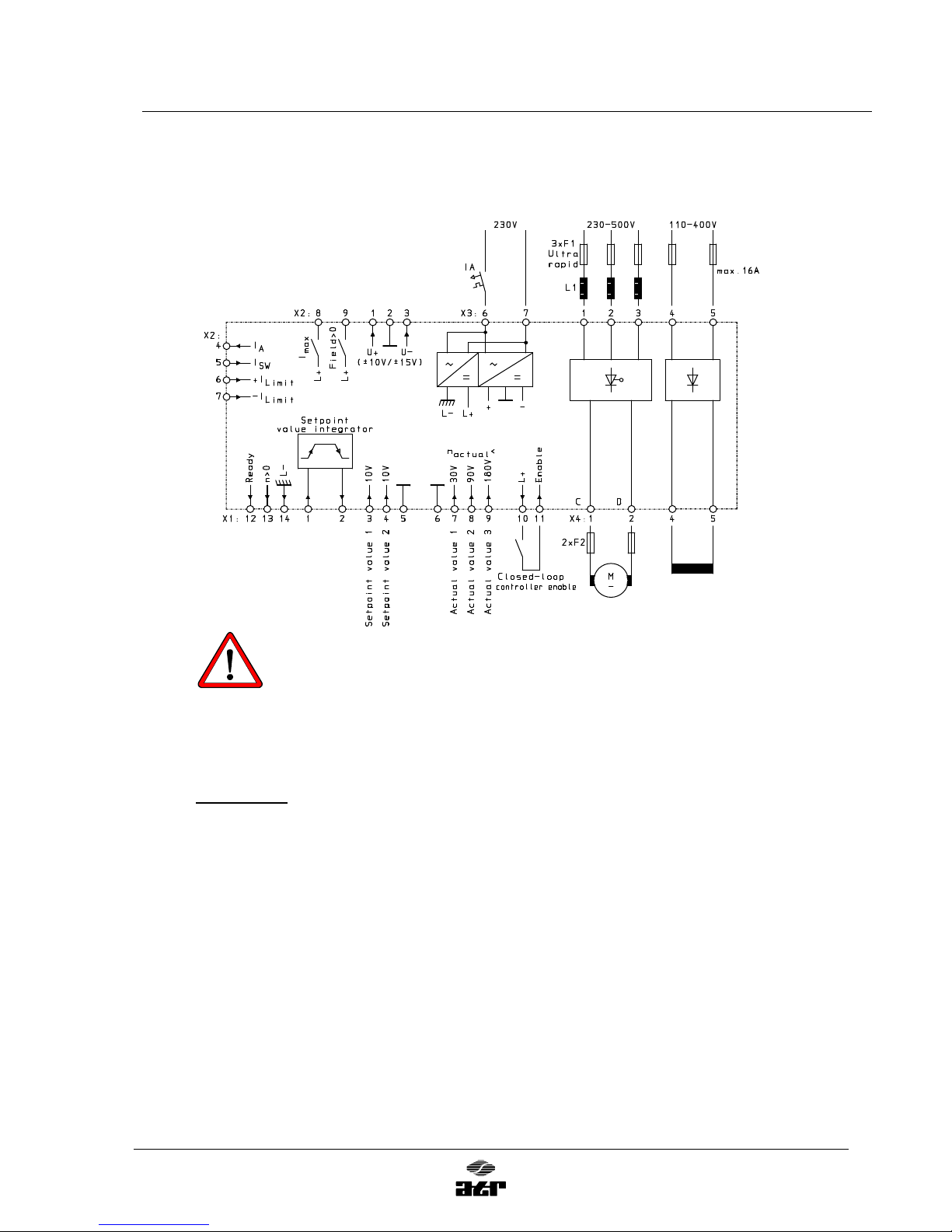
4 DEVICE CONNECTION
4.1 Connection Diagram
Danger
Incorrect connection of the device can lead to damage or destruction.
4.2 Sequence for Switching On/Off
Switching on
1. Field supply X3: 4 + 5
2. Electronics supply X3: 6 + 7
3. Main power X3: 1 + 2 + 3
4. Closed-loop controller enable X1: 10 + 11
5. Setpoint value X1: 1 or 3 or 4
Points 2 to 5 can be switched together, as the device is fitted with an internal inhibition of
approx. 200 ms after the electronics supply has been switched on. The "stand-by" signal is
also only given after this interval, however.
Point 1 must be switched on at least one second earlier than point 3.
The electronics supply can remain switched on permanently, it does not have to be switched
on and off with the drive.

Temvar GDE2
July 08, 2009
9
Switching off
1.) Setpoint X1: 1 or 3 or 4
2.) At standstill closed-loop controller enable X1: 10 + 11
3.) Main power X3: 1 + 2 + 3
4.) Field supply X3: 4 + 5
5.) Electronics supply
Points 1 and 2 can be switched together.
Points 3 to 5 can be switched together, but at least one second after point 2.
The electronics supply must not be switched off. The motor is safely isolated when points 1 - 4
have been switched off.
4.3 Terminal Assignment
X1: Electronics plug-in terminal 14-pole
1 Input setpoint value integrator max. ± 10 V. Input resistance 100 K.
2 Output setpoint value integrator max. ± 10 V. Output resistance 44 Ohm.
3 Setpoint value input max. + 10 V. Input resistance 44 K.
Filter time constants 22 ms.
4 Setpoint value input max. + 10 V. Input resistance 44 K.
Filter constants 22 ms.
5 Closed-loop controller ground
6 Closed-loop controller ground
7 Actual value input max. - 30 V. Input resistance 12 K.
8 Actual value input max. - 90 V. Input resistance 30 K.
9 Actual value input max. - 180 V. Input resistance 48 K.
10 L+, potential-free auxiliary voltage + 24 V for closed-loop controller enable, signal
outputs and auxiliary electronics. Load capacity max. 50 mA.
11 Input closed-loop controller enable via optocoupler + 18 to 30 V corresponds to >
12.5 V corresponds to closed-loop controller enable. Input resistance 3K3.
12 Output operational signal. + 24 V corresponds to "device stand-by".
Max. load capacity 20 mA.
13 Output operating signal. + 24 V corresponds to "drive turning".
Max. load capacity 20 mA.
14 L-, reference point of potential-free auxiliary voltage 24 V for closed-loop controller
enable, signal outputs and auxiliary electronics. Load capacity 50 mA.
X2: Electronics plug-in terminal 9-pole
1 Output + 15 V or + 10 V stabilized for auxiliary electronics and setpoint value
formation.
Max. load capacity 30 mA. The voltage can be determined using the jumper
(+15/+10).
2 Closed-loop controller ground
3 Output – 15 V or - 10 V stabilized for auxiliary electronics and setpoint value
formation. Max. load capacity 30 mA. The voltage can be determined using the
jumper (-15/-10).

Temvar GDE2
July 08, 2009
10
4 Output current actual value. Nominal device current corresponds to + 10 V.
Output resistance 220 Ohm.
5 Auxiliary input to current controller. + 10 V corresponds to 100% current setpoint
value.
Input resistance 44 K. Filter time constants 2.2 ms.
6 Input for external current limit setting + or - 10 V corresponds to 100% (R5 right
stop) current limit for positive speed setpoint value and drive operation.
Input resistance 4K7.
7 Input for external current limit setting for 4Q-device (R6 left stop).
Input resistance 4K7.
8 Signal output "current limit“ . + 24 V corresponds to device at current limit.
Max. load capacity 20 mA.
9 Signal output "field current“. + 24 V corresponds to field current larger than 0.2 A.
For devices above 380 A, field current larger than 0.4 A
Max. load capacity 20 mA.
Main power connections X3 + X4
Main current
supply
X3: 1 + 2 + 3
Field
supply
X3: 4 + 5
Electronics
supply
X3: 6 + 7
Armature
connection
X4: 1 + 2
Field
connection
X4: 4 + 5
GDE2-15 42 * 2.52 * 2.52 * 42 * 2.52 *
GDE2-30 42 * 2.52 * 2.52 * 42 * 2.52 *
GDE2-60 162 * 2.52 * 2.52 * 162 * 2.52 *
GDE2-90 162 * 2.52 * 2.52 * 352 * 2.52 *
GDE2-130 20 x 3/M8 ** 42 * 2.52 * 20 x 5/M8 ** 42 *
GDE2-190 20 x 3/M8 ** 42 * 2.52 * 20 x 5/M8 ** 42 *
GDE2-270 20 x 5/M8 ** 42 * 2.52 * 20 x 5/M8 ** 42 *
GDE2-380 40 x 5/M10 ** 42 * 2.52 * 40 x 5/M10 ** 42 *
GDE2-500 40 x 5/M10 ** 42 * 2.52 * 40 x 5/M10 ** 42 *
GDE2-700 40 x 5/M10 ** 42 * 2.52 * 40 x 5/M10 ** 42 *
* = Line-up terminals ** = Conductor rails

Temvar GDE2
July 08, 2009
11
4.4 Assembly
4.4.1 Danger
Incorrect lifting can lead to injury and damage to the equipment.
The device should only be lifted by qualified personnel using suitable equipment.
The device must be assembled in accordance with safety regulations (e.g. DIN, VDE)
and all other relevant national or local regulations. The device must be properly
grounded, with sufficient phase-to-ground clearance and corresponding short-circuit
protection, to ensure that a high level of operating safety is maintained.
4.4.2 Mechanical Design
For reasons of electromagnetic compatibility
(EMC), the devices have a galvanized steel
housing. For the same reason, a galvanized
mounting plate is recommended, along with
connecting the ground lead to a copper bus
connected to the mounting plate via a broad,
conductive surface area (see construction
suggestions).
In order to ensure an unimpeded flow of cooling
air, an interval of at least 100 mm above and
below the device must be kept clear of
obstruction.
Failure to observe this may lead to the device
overheating!
The main power fuses must be ultra fast
blowing semiconductor fuses.
4.4.3 Wiring Instructions
All leads connected to terminal strips X1 and X2
must be shielded. The shielding should be firmly
attached using terminals, clips, or binders,
across a broad contact surface on the bus bar
provided for that purpose. Analog signal leads
should only be grounded at one point. Leads
with binary control signals can be grounded at
several points. The wiring paths should be kept
short and the electronics wiring should be
strictly isolated from the main current wiring.
(see the construction suggestions).
The closed-loop controller ground should be
connected to the protective circuit by a short
2.52 stranded wire.
Temvar GDE2
July 08, 2009
12
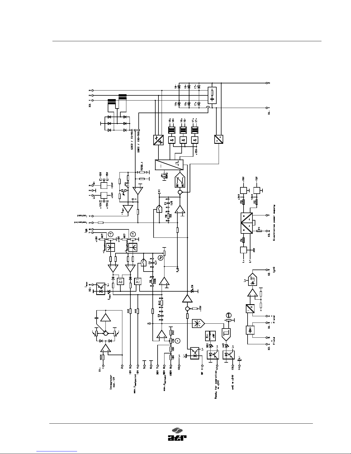
5 LAYOUT PLANS
5.1 Circuit Diagram

Temvar GDE2
July 08, 2009
13
5.2 Equipment Configuration
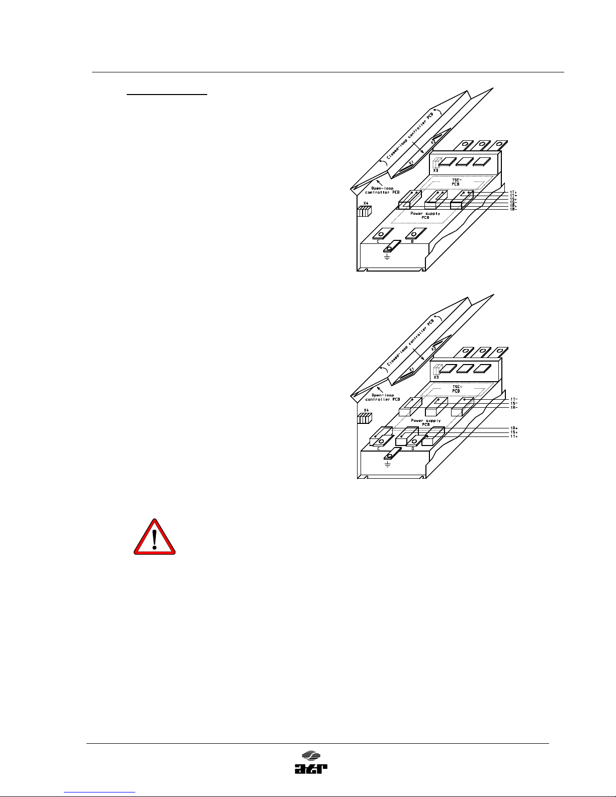
Thyristor module:
GDE2-15 3 x MCC 19-16io8B
GDE2-30 3 x MCC 19-16io8B
GDE2-60 3 x MCC 44-16io8B
GDE2-90 3 x MCC 44-16io8B
The miniature fuses for the electronic supply are
located on the supply module.
This module can be accessed when the closedloop controller PCB is lifted out the way in the
direction of the arrow.
X1: Electronics terminal strip
Main function
X2: Electronics terminal strip
Main function
X3: Input terminals
Main power
X4: Output terminals
Main power
Thyristor module:
GDE2-130 3 x MCC 95-16io8B
GDE2-190 3 x MCC 95-16io8B
GDE2-270 3 x MCC 132-16io8B
The miniature fuses for the electronics supply
are located on the supply module.
This module can be accessed when the closedloop controller PCB is lifted out of the way in the
direction of the arrow.
X1: Electronics terminal strip
Main function
X2: Electronics terminal strip
Auxiliary function
X3: Input terminals
Main power
X4: Output terminals
Main power
Temvar GDE2
July 08, 2009
14
Thyristor module:
GDE2-380 3 x MCC 170-16io8B
GDE2-500 3 x MCC 255-16io8B
GDE2-700 6 x MCC 312-16io8B
The miniature fuses for the electronics supply
are located on the supply module.
This module can be accessed when the closedloop controller PCB is lifted out of the way in the
direction of the arrow.
X1: Electronics terminal strip
Main function
X2: Electronics terminal strip
Auxiliary function
X3: Input terminals
Main power
X4: Output terminals
Main power
Danger
Dangerous voltage is present even when the system switch of the power controller is
open. The control module and supply modules contain a number of dangerous live
circuits.
Failure to observe the instructions given in this operating manual can cause death,
serious injury to persons, and damage to equipment.

Temvar GDE2
July 08, 2009
15
5.3 Component Mounting Diagram for Electronics PCBs
Open-loop controller PCB Closed-loop controller PCB
GDE2 GDE2
(A0095xx) (A0114xx)

Temvar GDE2
July 08, 2009
16
SUPPLY PCB
For devices up to 270 A
SUPPLY MODULE
For devices above 380A

Temvar GDE2
July 08, 2009
17
5.4 Potentiometer Settings
+B Setpoint value integrator. Acceleration time for positive setpoint value.
Left stop approx. 1.5 seconds, right stop approx. 15 seconds.
R1 Acceleration time from 0 to 10 V.
-B Setpoint value integrator. Delay time for positive setpoint value. Effect as with + B.
R2
Vp Proportional gain for the speed controller. Left stop = x2.
Right stop = x20. This area is determined by R9 as delivered.
R3
n 25-turn spindle potentiometer for speed adjustment. Setting range approx. 1 : 4
R4 Right-hand rotation means higher speed.
+I Current limit for motor-driven operation and positive speed setpoint value or
generator-driven operation and negative speed setpoint value. Left-hand stop
R5 causes current limit 0, right-hand stop 100% of the nominal device current.
-I R6 Current limit for 4 Q device (left-hand stop).
n > 0 Threshold of operating signal 0 to 15% of the maximum speed can be set.
R7 Right stop is equal to 15%.

Temvar GDE2
July 08, 2009
18
5.5 LED Displays
STAND-BY
LED lights up when all internal electronic voltages are okay.
As soon as the closed-loop controller is enabled, the system voltage is also
checked.
Main power with clockwise rotating field, phase failure and tacho monitoring.
CLOSED-LOOP CONTROLLER ENABLE
LED lights up when the device is ready and the closed-loop controller on terminal
11 is enabled by the + 24 V signal.
n > o
LED lights up if the drive rotates faster than the threshold value set on the
potentiometer n > 0.
Current direction "+"
LED indicates 1Q operation.
Current direction "-"
This signal is only in use for the 4 Q device.
Current limit
LED lights up if the motor is driven at the set current limit for at least 15 seconds,
i.e., the speed controller is operated up to the stop, which is set with the
potentiometer +I.
Tacho
LED lights up when the tacho voltage is not at the ratio to the armature voltage
specified.
System power
LED lights up if the system power is not with clockwise rotating field, in the event
of phase failure or overheating of the heat sink.
⊗⊗⊗⊗
⊗⊗⊗⊗
⊗⊗⊗⊗
⊗⊗⊗⊗
⊗⊗⊗⊗
⊗⊗⊗⊗
⊗⊗⊗⊗
⊗⊗⊗⊗

Temvar GDE2
July 08, 2009
19
6 FUNCTIONAL DESCRIPTION OF THE INPUTS AND OUTPUTS
6.1 Analog Inputs
The analog inputs may only be connected using shielded leads. The shield should only be
connected to the grounding system at one point, across a broad contact surface in close
proximity to the device. For reasons of electromagnetic compatibility, these leads may never
be operated open-circuit, they must be connected with respect to the electrical ground when
the device is switched off.
Setpoint value integrator
The input voltage range is ± 0 to 10 V.
Setpoint value inputs
The two inputs are equal and are added together.
The maximum input voltage range is ± 0 to 10 V.
Input resistance and filter time constant are 44 KOhm and 22 ms respectively.
Actual value inputs
The potentiometer "speed adjustment" is a 25speed spindle potentiometer with a setting range
of approx. n = 4.
Right-hand stop means highest speed.
The filter time constant is selected at a very low
level of approx. 2.2 ms for reasons of dynamics,
the tacho voltage must therefore be very clean.
Inputs "external current limit"
The maximum motor current is set using
potentiometer +I (right stop 100% nominal device
current).
An external voltage of 0 to 10 V at X2: 6 means 0
to 100% motor current.
The input is equipped with an active rectifier and
can therefore process + 10 V or - 10 V (input
resistance 4K7).
The set current limit can also be reduced by
connecting a resistor to ground.
There is only a negative current limit for the 4 Q
device. For this device, the potentiometer -I is set
to the left stop.

Temvar GDE2
July 08, 2009
20
Auxiliary input - current controller
A voltage of + 10 V at terminal X2: 5 means
nominal device current.
Caution!
This auxiliary setpoint value is added to the main
setpoint value from the speed controller. The
current limit must be set low enough to ensure that
the sum of the two setpoint values does not
exceed + 10V. This input has a very low filter time
constant (2.2 ms), the voltage at terminal X2: 5
must therefore be very clean.
6.2 Analog Outputs
Setpoint value integrator
The output is protected against reverse
interference voltage by a lowpass filter and pull-up
diodes. This leads to a minimum influence of load
variation, which is however completely irrelevant if
the load is constant (e.g. with a connection to
setpoint value inputs X1: 3 or 4).
Actual current value
With a nominal device current, a voltage of + 10 V
is supplied.
Output resistance 220 Ohm.

Temvar GDE2
July 08, 2009
21
6.3 Control Inputs and Signal Outputs
Inputs and outputs are separated from the electronics potential by optocouplers. They have
their own 24 V system power supply, designated with +L and -L.
The reference potential -L, terminal X1: 14, is to be connected to the reference potential of the
system controls. It is recommended that these inputs and outputs also be connected with
shielded wire.
Danger
When controlling the binary control and selection inputs from an external voltage
source which is not connected to the device ground (X1: 14 not connected to X1: 5 or 6)
the potential difference between device ground and ground of the external voltage must
not exceed 50 V (danger for optocouplers).
Input - closed-loop controller enable
Closed-loop controller enable means: connect
voltage +L to terminal X1: 11, or apply an external
voltage of +15 to +30 V, with its reference point
connected to -L (terminal X1: 14). For a voltage
which is smaller than +10 V, the closed-loop
controller is safely inhibited. With an inhibited
closed-loop controller, the firing pulses are also
suppressed, the drive does not drift at a standstill,
but neither can it create torque. When the drive is
switched off, the closed-loop controller must be
inhibited at least 200 ms before the main power is
switched off.

Temvar GDE2
July 08, 2009
22
Signal output "stand-by"
Terminal X1: 12 is supplied with voltage +L if the
electronics power supply is present. As soon as the
closed-loop controller is enabled, the main power
is also checked at terminals X3: 1 + 2 + 3. For
devices with fans, this stand-by signal also
incorporates a temperature switch.
The stand-by signal is cancelled at a heat sink
temperature of more than 85° C. The output is
short-circuit proof.
Signal output n > o
Terminal X1: 13 is supplied by +L if the drive
turns faster than the threshold value set on the
potentiometer n > 0.
The signal is independent of the rotational
direction. The output is short-circuit proof.
Signal output "I max."
Terminal X2: 8 is supplied by +L if the drive is
operated at the maximum set current limit for
more than 15 seconds. The output is short-circuit
proof.
Signal output " field current present"
This output is only relevant if the field rectifier in
the device - terminals X3: 4 + 5/ X4: 4 + 5 - is
used.
Terminal X2: 9 is supplied by +L, if the field
current is greater than 0.2 A. For devices above
380 A, for a field current greater than 0.4 A. This
signal is not displayed by a light-emitting diode.
The output is short-circuit proof.

Temvar GDE2
July 08, 2009
23
7 FUNCTIONAL DESCRIPTION
7.1 Setpoint Value Integrator
With a positive setpoint step-change at terminal X1: 1, the comparator (1) inverts into the
negative. The capacitor C is charged via resistor R+. The rate of charge depends on the
position of the potentiometer +B. When the output voltage on integrator (2) reaches the level of
the setpoint value at X1: 1, the comparator (1) returns to 0 and the capacitor C is no longer
charged.
With a negative setpoint value, the same applies via potentiometer -B and charging resistor R-.
If a positive setpoint value is reduced abruptly, the comparator (1) tips into the positive range,
capacitor C is discharged via potentiometer -B and resistor R-.

Temvar GDE2
July 08, 2009
24
7.2 Speed Controller
The speed controller is a standard PI-controller. Proportional gain is determined by R9 and
potentiometer VP and the integral-action time by C2. Right-hand stop of the potentiometer VP
is equal to the largest gain. The closed-loop controller output can be measured at test point
"Xn". The PI-controller can be expanded to a PID-controller by means of C3 and R10. The
current speed, normalized at the level of the setpoint value, can be measured at test point "n“.
7.3 Current Limit
Comparators (1) and (2) are set to a bias voltage of between 0 and 10 V via potentiometers +l and l. Comparator (1) is tipped to positive, comparator (2) to negative. If the speed controller output
(point 3) exceeds the bias voltage set, the corresponding comparator is tipped up. Via the
corresponding diode and the relatively low resistor 4K7 on the merge point of the speed controller
(point 1) the closed-loop controller output is lowered again. At the same time, comparator (3) will tip
into the positive and, with a FET-switch, will short circuit capacitor C2 via the speed controller. This
circuit is designed for 4Q operation. As the GDE device series only allows 1Q operation, the
potentiometer -I is turned to the left-hand stop. The bias voltage of maximum 10 V can also be
connected externally to terminals X2: 6 (input resistor 4K7).

Temvar GDE2
July 08, 2009
25
7.4 Current Controller
T
he current controller is a standard PI-controller. Proportional gain is determined by R8, the
integral-action time by C1. When using auxiliary input X2: 5, it must be taken into consideration
that the two setpoint values add up. Together they must not exceed + 10 V. The current
controller output can be measured at test point -XI. Terminal X2: 4 is supplied with the actual
current value + 10 V at nominal device current. The voltage is equalized with a time constant of
200 ms.
The actual current value is created on the open-loop controller PCB. By increasing the
effective load resistance R161/R161.1 and relocating jumpers J3/J4, all values can be kept
below the nominal device current level. Decreasing the effective load resistance is not
permitted.
Danger
If auxiliary input X2: 5 is used, the device and the motor can be overloaded or the drive
run up to excessive speeds. The current limit is not effective at input X2: 5.
7.5 Firing Pulse Formation
The output voltage of the current controller is added to the actual armature voltage. This
relieves the current controller and causes the controller to act more dynamically. The
integrated firing pulse module is controlled with the sum of these two voltages. The firing
pulses last for approx. 1 ms and are chopped at a 100 µs rate.
The rectifier limit (GG) is fixed, the inverter limit (WG) is set ex works and must not be
changed. For 60 Hz operation, bridge JP2 must be fitted on the open-loop controller PCB.

Temvar GDE2
July 08, 2009
26
7.6 Thyristor Outputs
The selected current direction +I activates
the corresponding pulse transformers and
clears the AND-gates for the firing pulses.
The thyristors require a holding current of
approx. 100 mA. If this current is not
achieved during the firing phase, the
thyristor blocks again after the firing pulse
has been removed.
7.7 Electronics Supply
To supply the electronics, a system power
source of 230 V/50-60 Hz is required. ± 10%
tolerance is permissible. Slow blowing
subminiature fuses are used. The ± 15 V
and L+ /L- are stabilized with linear
regulators.
The ± 24 V are only filtered.
7.8 Field Supply
The rectifier can be connected to a
maximum 400 V and carry a maximum load
of 5 A (above GDE2/380 max. 15 A). At a
current of greater than 0.2 A (for devices
above 380 A greater than 0.4 A) potential +L
is present at signal output X2: 9. The output
is short-circuit proof.

Temvar GDE2
July 08, 2009
27
7.9 System Power Supply Monitoring
In the case of an anti-clockwise rotating
field or phase failure, a fault alarm flag is
set, the closed-loop controller and firing
pulse formation are blocked. The "standby" signal is cancelled and the red warning
lamp "mains“ lights up. The signal flag is
reset by switching off the electronics
supply for at least 2 seconds or by
actuating reset button S2 on the closedloop controller PCB.
7.10 Tacho Monitoring
The tacho and the closed armature circuit
are monitored by the armature voltage
being compared with the tacho voltage,
normalized at 10 V. With a constant field
excitation the tacho voltage is directly
proportional to the armature voltage. At
the initial set-up, the 10 V tacho voltage
has not yet been normalized to 100%
armature voltage. Therefore, the device
should be switched on for the first time
with a speed setpoint value of approx. 1 V.
The speed adjustment with 10 V setpoint
value can only be made when the tacho
monitor is switched off. This is achieved by
closing the Dip-Fix switch S1 on the
closed-loop controller PCB. If the
normalized tacho voltage is approx. 30%
below the armature voltage (100% UA =
10 V) or the tacho is incorrectly poled, the
fault alarm flag is set (see Section 7.9).
7.11 Fan Monitoring
With the exception of the 15 + 30 A
devices, all devices have a fan for cooling
purposes. The heat sink temperature is
monitored on these devices by an 85°
bimetallic thermal switch. The actuated
(opened) switch has the same effect on
the device as the system power supply
monitoring (Section 7.9).

Temvar GDE2
July 08, 2009
28
8 INSTALLATION
8.1 Dangers
When this device is operated, certain parts of it are automatically under dangerous
voltages, which can lead to serious bodily injury or death. The following precautionary
measures must be followed to minimize the risk of injury or death.
1. Only qualified personnel who are familiar with the device and the information
supplied are permitted to assemble and operate the device, to seek and rectify faults
and carry out repairs.
2. The device must be fitted in accordance with safety regulations (e.g. DIN, VDE) and
all other relevant national or local regulations. The device must be properly
grounded, with adequate wire sizing, and corresponding short-circuit protection, to
ensure that a high level of operating safety is maintained.
3. During normal operation, all covers and doors must remain closed.
4. Before carrying out checks and maintenance work, it must be ensured that the AC
power supply is switched off and locked.
Both the power controller device and the motor are live before the AC power supply
is switched off. Voltage is present even if the contactor of the power controller is
open.
5. If measurements have to be made when the power supply is switched on, contact
with the electrical connection points must be avoided at all times. Remove all
jewellery from wrists and fingers. Ensure that the testing equipment is in full and
safe working order.
6. When working on the live machine, stand on insulated flooring, i.e. make sure that
there is no ground connection.
7. Follow the instructions given in this manual closely and observe all danger, warning
and caution advisories.
8. This list is not a comprehensive list of all measures required for the safe operation of
the machine. If you require further information or if particular problems arise, please
contact the manufacturer.

Temvar GDE2
July 08, 2009
29
8.2 Recommended Procedure
Dangers
Up until installation point 4 the device must remain isolated from the power supply. The
drive will start once the closed-loop controller is enabled!
1. Check that all main power ground wires and electronic terminals are connected
correctly. Check fuses in accordance with the device table in 3.1.
2. Use an ohmmeter to check the armature connection (1 - 10 OHM),
field connection (100 - 500 OHM) and tacho connection (approx. 80 OHM).
3. Set potentiometer +I to approx. 30%, all other potentiometers to the left-hand stop.
Release the connection for closed-loop controller enable terminal X1: 11.
Disconnect setpoint value (terminal X1: 1 or 3 or 4) and manual potentiometer to
terminal X2: 1 + 2.
Connect collector ring to X1: 3. Voltage selection terminal X2: 1 to 10 V.
Determine the maximum tacho voltage expected and check that the correct actual
value input is being used. Connect volt meter to this terminal.
4. Switch on the device and measure the main power at terminal X3: 1 + 2 + 3, field
supply X3: 4 + 5, electronics supply X3: 6 + 7, field voltage X4: 4 + 5. Set the setpoint
value to approx. + 1 V using the manual potentiometer.
5. Briefly tap the free wire "closed-loop controller enable" against terminal X1: 11. The
volt meter on the actual value input must deflect negatively. In this case the wire can
be fixed in position and the rotational direction of the machine checked. If the rotational
direction is incorrect reverse the poles of the field and tacho connections.
6. Set the current limit to the nominal motor current. Set the setpoint value potentiometer
to +10 V and deactivate tacho monitoring function (S1). Adjust the speed using spindle
potentiometer "n". The armature voltage must not exceed the value on the type plate,
if necessary reduce the field current. After adjusting the speed, reactivate the tacho
monitoring function.
Danger
Too large an overshoot can lead to the permissible armature voltage being exceeded.
Abrupt changes to the setpoint value in the field weakening range can lead to the
armature current overshooting.
7. Pinch off the manual potentiometer, apply device setpoint value and test the
emergency off function with the device setpoint value.

Temvar GDE2
July 08, 2009
30
9 OPTIMISATION
For most applications, the standard assignment for the current and speed controllers is fully
sufficient. It is advisable, however, to check the transient response of the motor in the event of
abrupt changes in the setpoint value and to optimize this using potentiometer VP . If a critical
drive requires more precise optimization, the following procedure is recommended after the
drive has been placed in operation.
The speed controller should be optimized with a machine connected.
A) Optimizing the current controller
1. Connect the potentiometer for the setpoint value and switch for closed-loop
controller enable according to the following diagram
2. Connect the speed controller according to diagram. VP-potentiometer to lefthand stop.
3. Connect RC decade according to diagram. Begin with the standard
assignment. Connect oscilloscope to test point "I".
4. Pinch off the field supply. Bridge the field current monitoring function.
5. Switch on the drive, enable the closed-loop controller. Use the potentiometer
at terminal 3 to set the even, ripple-free current. Use switch SW to set setpoint
value change. Optimize current controller first with R8, then with C1 so that the
oscillogram appears similar to the one shown in the diagram.
B) Optimizing the speed controller
1. Connect potentiometer for speed setpoint value, switch for closed-loop
controller enable and RC decade according to the following diagram.

Temvar GDE2
July 08, 2009
31
2. Connect the field supply. Set the RC decade to standard assignment
V
P
-potentiometer to center point.
3. Switch on the drive, enable the closed-loop controller.
Set approx. 30% of the maximum speed and enter the setpoint value change
using switch SW. Optimize speed controller first with R9, then with C2 so that
the oscillogram appears similar to the one shown in the diagram. The transient
response of the speed controller can often be improved using a D-element
R10/C3, particularly when accelerating or positioning large masses.
Dimensioning guidelines are in the range of 22 K and 1µF.
10 FAULT OCCURRENCE
Dangers
During operation of electrical devices, certain parts are subject to dangerous voltage.
The signal relay of the customer can be subject to dangerous voltage.
Incorrect use of these devices can therefore lead to death or serious injury as well as
serious material damage.
For this reason, observe all the instructions in this section and on the device itself
when carrying out maintenance work.
Maintenance on the device may only be carried out by authorized personnel, who are
fully versed in the safety instructions, assembly, operating and servicing instructions
contained in this manual.
Before carrying out checks and maintenance work, it must be ensured that the AC
power supply is switched off and locked and that the device is grounded.
Both the power controller device and the motor are live before the AC power supply is
switched off. Voltage is present even if the contactor of the power controller is open.
Only spare parts allowed by the manufacturer may be used.
A) Main power fuse defective.
Check the thyristors : Take measurements at terminals X3: 1 + 2, X3: 2 + 3 and X3: 1
+ 3 using an ohmmeter.
Resistance must be above 40 K-Ohm.
Measure from X3: 1 to X4.1, then X3: 2 to X4.1 and X3: 3 to X4.1, resistance must be
more than 100 K-Ohm.
Measure from X3: 1 to X4.2, then X3: 2 to X4.2 and X3: 3 to X4.2, resistance must be
more than 100 K-Ohm.

Temvar GDE2
July 08, 2009
32
B) Drive is not turning. Assuming:
Wiring and fuses are okay.
Switch on drive - positive setpoint value.
Light-emitting diodes:
⊗
Stand-by On Off On On On Off Off
⊗
Cl.-loop controller
enable
On Off Off On On Off Off
⊗
n > 0 Off Off Off Off Off Off Off
⊗
Current direction + On Off Off On On On On
⊗
Current direction - Off Off Off Off Off Off Off
⊗
Current limit Off Off Off Off On Off Off
⊗
Tacho Off Off Off Off Off Off On
⊗
Power system Off Off Off Off On On Off
Case
1
2
3
4
5
6
7
Case 1: Setpoint value at terminal X1: 3 or 4 against reference point X1: 5 or 6
probably missing.
Case 2: Measure electronics supply ± 15 V or ± 10 V at terminals X2: 1 + 3. If
missing, check supply at X3: 6 + 7 and miniature fuses F1, F2, F3 on the
supply module.
Case 3: Closed-loop controller enable missing. Measure + 24V at terminal X1: 11
against reference point X1: 14. If not available, check the miniature fuse F4
on the supply module.
Case 4: Potentiometer current limit +I is turned to zero.
Case 5: Potentiometer current limit +I is not turned up enough. Measure output
voltage at X4: 1 + 2. If present, armature line is interrupted.
Case 6: Phase failure, rotational field incorrect, measure main connection voltage at
X3: 1 + 2. Check the thermal contact for GEV2/40.
Case 7: Normalized tacho actual value 30% smaller than normalized armature
voltage, tacho input line interrupted, drive mechanically blocked.
 Loading...