

查询U2044B 供应商
Dual Output Flasher
Description
The integrated circuit U2044B is used in relay-controlled
automotive flashers. With two output stages, each side of
the vehicle is controlled separately. A left and a right
direction indicator input with only a small control current
makes switch contacts for small loads possible.
Features
Temperature and supply voltage compensated
flashing frequency
Frequency doubling indicates lamp outage
Two relay driver outputs with high current-carrying
capacity and low saturation voltage
U2044B
The separate hazard warning input simplifies the
construction of the hazard switch. Lamp outage is indicated by frequency doubling during direction mode.
Thanks to the extreme low current consumption the
U2044B can be connected to the battery directly.
Very low susceptibility to EMI
Protection according to ISO/TR7637/1 level 4
Extremly low current consumption < 10 A
(@switches open)
Reverse polarity protection
Minimum lamp load for flasher operation: 1 W
Three control inputs: left, right and hazard warning
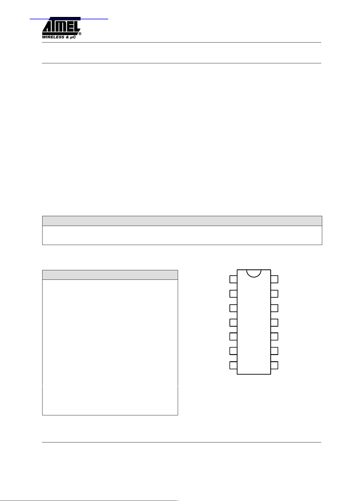
Ordering Information
Extended Type Number Package Remarks
U2044B DIP14
U2044B-FP SO14
Pin Description
Pin Symbol Function
1 OSC Oscillator
2 SIL Start input left
3 SIR Start input right
4 SIHW Start input hazard warning
5 V
V
S
S
6 CR1 Control input relay 1
7 CR2 Control input relay 2
8 LD Lamp failure detection
9 V
V
S
S
10 GND IC ground
11 OR1 Output relay 1
12 V
V
S
S
13 OR2 Output relay 2
14 OSC Oscillator
OSC
SIL
SIR
SIHW
V
CR1
CR2
1
2
3
4
U2044B
S
5
6
7
Figure 1. Pinning
10
14
13
12
11
OSC
OR2
Vs
OR1
GND
9
V
S
LD
8
12750
Rev. A4, 03-Apr-01 1 (6)
U2044B
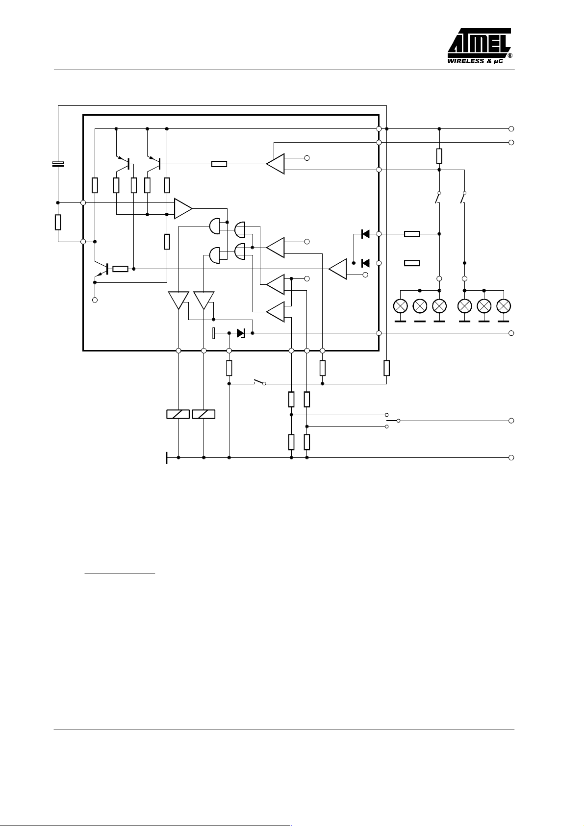
Block Diagram
C
4.7 F
R
1
82 k
9
5
R
VS–81 mV
V
Ref1
+
–
V
Ref2
R
3
4.7 k
R
4
6
4.7 k
8
R
R
10
1.2 k
9
47 k
R
8
47 k
6
7
/2
V
S
12
right
K1
4.7 k
+
–
+
–
–
+
–
+
R
1
14
1
VS–6 V
+
–
Relay
12
27.5 V
GND 101311 3 2 4
R
2
220
Hazard warning
Shunt
30 m
Contact
12
30
30
30
15
1.2 k
Figure 2. Application circuit
R
for protection against continous reversed polarity: 1 W att
2
Functional Description
Pin 1 and Pin 14, Oscillator
Flashing frequency, f1, is determined by the R1C
components as follows (see figure 2):
f
1
R1 C1 1.5
where C1 47 F
In the case of a lamp outage, the oscillator frequency is
switched to the lamp outage frequency f2 with
f2 2.2 f1.
Duty cycle in normal flashing mode: 50%
Duty cycle in lamp outage mode (bright phase): 40%
1
Hz
R1 6.8 k to 180 k
R
R
5
7
1.2 k
left
Pin 2 and Pin 3, Start input right and left
Flashing is disabled as long as the input comparator is tied
1
to GND (pull-down resistor R7 or R5). The high-side
flasher switch ”left” or ”right” changes the comparator
status and enables the output stage at Pin 11 or Pin 13. R
and R4 are protection resistors for the input stage.
With an open flasher switch the current consumption is
only I 10 A. The IC is kept in stand-by mode until
there is a voltage drop of V 6.9 V at the pull-down resistor.
Direction mode can only be activated when the ignition
switch is in ON-position as shown in figure 2.
31
12700
6
Rev. A4, 03-Apr-012 (6)

U2044B
Pin 4, Start input hazard warnig
In contrast to the direction switches, the hazard input is
a low-side type. The pull-up resistor R10 provides the offstate. R3 is a protection resistor for the input stage.
Hazard warning can be activated independent of the ignition switch position.
Pin 5, Supply voltage sense
This pin supplies the lamp outage comparator at Pin 8 and
is externally connected to the battery (Kl 30).
Pin 6 and 7, Control input relay 1 and 2
The feedback detects the bright phase and the dark phase
and enables the oscillator.
Pin 8, Lamp outage detection
The lamp current is monitored via an external shunt
resistor, R
reference voltage of typ. 81 mV (V
and an internal comparator K1 with its
Shunt
= 12 V). The outage
S
of one lamp out of two lamps is detected according to the
following calculation:
Nominal current of 1 lamp: 21 W / (V
I
= 1.75 A
lamp
Nominal current of 2 lamps: 2 x 21 W / (V
I
= 3.5 A.
lamp
= 12 V):
S
= 12 V):
S
The detection threshold is recommended to be set in the
middle of the current range: I
outage
2.7 A
Thus the shunt resistor is calculated as:
R
= V
Shunt
(K1) / I
T
outage
R
= 81 mV/2.7 A = 30 m.
Shunt
Comparator K1‘s reference voltage is matched to the
characteristics of filament lamps (see “control signal
threshold” in the data part).
The combination of shunt resistor and resistance of wire
harness prevents Pin 8 from a too high voltage in the case
of shorted lamps.
Pin 9, Supply voltage
This pin supplies the oscillator, the comparators and the
logic parts of the IC.
Pin 10, GND
The integrated circuit is protected against transients
according to ISO–TR 7637–3 level 3 via resistor R2 to
ground (–31). An integrated protection circuit together
with external resistors R
2, R3, R4, R6, R8
and R
limits the
9
current pulses in the IC. The IC is also protected against
reversed battery.
Pin 11 and 13, Control output relay 1 and 2
The relay control outputs are high-side driver with a low
saturation voltage and capable to drive a typical
automotive relay with a coil resistance of 60
Pin 12, Supply voltage power
This pin supplies the relay drivers connected directly to
the battery (Kl 30). It is internally clamped by a 27-V
Z-diode.
Absolute Maximum Ratings
Reference point ground (terminal 31), with external circuitry.
Parameters Symbol Value Unit
Supply voltage, 1 min Pins 5, 9, 12 V
Junction temperature T
Storage temperature range T
Ambient temperature range T
Thermal Resistance
Parameters Symbol Value Unit
Junction ambient DIP14
SO14
R
R
S
j
stg
amb
thJA
thJA
24 V
150 °C
–55 to +150 °C
–40 to +100 °C
90
120
K/W
K/W
Rev. A4, 03-Apr-01 3 (6)

U2044B
Electrical Characteristics
Typical values under normal operation in application circuit figure 1, VS (+30) = 12 V.
Reference point ground (–31), T
Parameters Test Conditions / Pins Symbol Min. Typ. Max. Unit
Supply voltage range Pins 5, 9, 12 V
Supply current, switches open Pins 5, 9, 12 I
Output current for relay driver Pins 11, 13 I
Saturation voltage R
Relay coil resistance R
Relay output,
reverse current
Start delay (first bright phase) t
Control signal threshold VS = 9 V Pin 8
Tolerance of control signal
threshold
Temperature coefficient of
control signal threshold
Clamping voltage T
Relay output overvoltage
detection (relay disabled)
= 25°C, unless otherwise specified.
amb
8 18 V
= 82 Pins 11, 13
L
VS = 8 V
S
S
O
V
O
VS = 12 V
60
Pins 11, 13 I
V
L
O
ON
S
VS = 13.5 V
VS = 16 V
VS = 9 to 16 V, Pin 8
T
= –40 to +100°C –6 +6 %
amb
VS = 13.5 V Pin 8 T
= –40 to +100°C V
amb
T
= –40 to +100°C V
amb
12
12
K
25.0 27.5 30.0 V
18 20 22 V
10 A
300 mA
1.0
1.2
0.1 mA
10 ms
70.6
85.0
93.0
mV
mV
mV
10 V/K
V
V
Tolerances
tVS = 9 to 18 V, T
Parameters Test Conditions / Pins Symbol Min. Typ. Max. Unit
Frequency determining
resistor
Frequency determining
capacitor
Frequency tolerance
(normal flashing basic frequency f1 not including the
tolerance of the external
components R1 and C1)
Bright period (basic frequency f1)
Bright period
(control frequency f2)
Frequency increase
(lamp failure)
Lamp load P
= –40 to +100°C
amb
R
C
f
F
f
f
1
1
1
1
2
2
L
6.8 510 k
47 F
–5 +5 %
47 53 %
37 45 %
2.15 f
1
2.3 f
1
1 W
Hz
Rev. A4, 03-Apr-014 (6)

Package Information
Package DIP14
Dimensions in mm
20.0 max
U2044B
7.77
7.47
4.8 max
Package SO14
Dimensions in mm
3.3
0.5 min
1.64
0.58
1.44
0.48
15.24
14 8
17
8.75
2.54
technical drawings
according to DIN
specifications
6.4 max
0.36 max
9.8
8.2
5.2
4.8
3.7
13020
1.4
0.4
1.27
7.62
14 8
14 8
0.25
0.10
3.8
6.15
5.85
technical drawings
according to DIN
specifications
0.2
13035
Rev. A4, 03-Apr-01 5 (6)

U2044B
Ozone Depleting Substances Policy Statement
It is the policy of Atmel Germany GmbH to
1. Meet all present and future national and international statutory requirements.
2. Regularly and continuously improve the performance of our products, processes, distribution and operating systems
with respect to their impact on the health and safety of our employees and the public, as well as their impact on
the environment.
It is particular concern to control or eliminate releases of those substances into the atmosphere which are known as
ozone depleting substances (ODSs).
The Montreal Protocol (1987) and its London Amendments (1990) intend to severely restrict the use of ODSs and forbid
their use within the next ten years. Various national and international initiatives are pressing for an earlier ban on these
substances.
Atmel Germany GmbH has been able to use its policy of continuous improvements to eliminate the use of ODSs listed
in the following documents.
1. Annex A, B and list of transitional substances of the Montreal Protocol and the London Amendments respectively
2. Class I and II ozone depleting substances in the Clean Air Act Amendments of 1990 by the Environmental
Protection Agency (EPA) in the USA
3. Council Decision 88/540/EEC and 91/690/EEC Annex A, B and C (transitional substances) respectively.
Atmel Germany GmbH can certify that our semiconductors are not manufactured with ozone depleting substances
and do not contain such substances.
We reserve the right to make changes to improve technical design and may do so without further notice.
Parameters can vary in different applications. All operating parameters must be validated for each customer
application by the customer. Should the buyer use Atmel Wireless & Microcontrollers products for any unintended
or unauthorized application, the buyer shall indemnify Atmel Wireless & Microcontrollers against all claims,
costs, damages, and expenses, arising out of, directly or indirectly, any claim of personal damage, injury or death
associated with such unintended or unauthorized use.
Data sheets can also be retrieved from the Internet: http://www.atmel–wm.com
Atmel Germany GmbH, P.O.B. 3535, D-74025 Heilbronn, Germany
Telephone: 49 (0)7131 67 2594, Fax number: 49 (0)7131 67 2423
Rev. A4, 03-Apr-016 (6)
 Loading...