

Page 1
Phase Control Circuit for Current Feedback
Description
The U2010B is designed as a phase-control circuit in
bipolar technology. It enables load-current detection and
has a soft-start function as well as reference voltage
Features
D
Full wave current sensing
D
Mains supply variation compensated
D
Programmable load-current limitation
with over- and high-load output
D
Variable soft-start
D
Voltage and current synchronization
D
Automatic retriggering switchable
D
Triggering pulse typical 125 mA
output. Motor control with load-current feedback and
overload protection are preferred applications.
D
Internal supply voltage monitoring
D
Current requirement v 3 mA
D
Temperature compensated reference voltage
Applications
D
Advanced motor control
D
Grinder
D
Drilling machine
U2010B
Package: DIP16, SO16
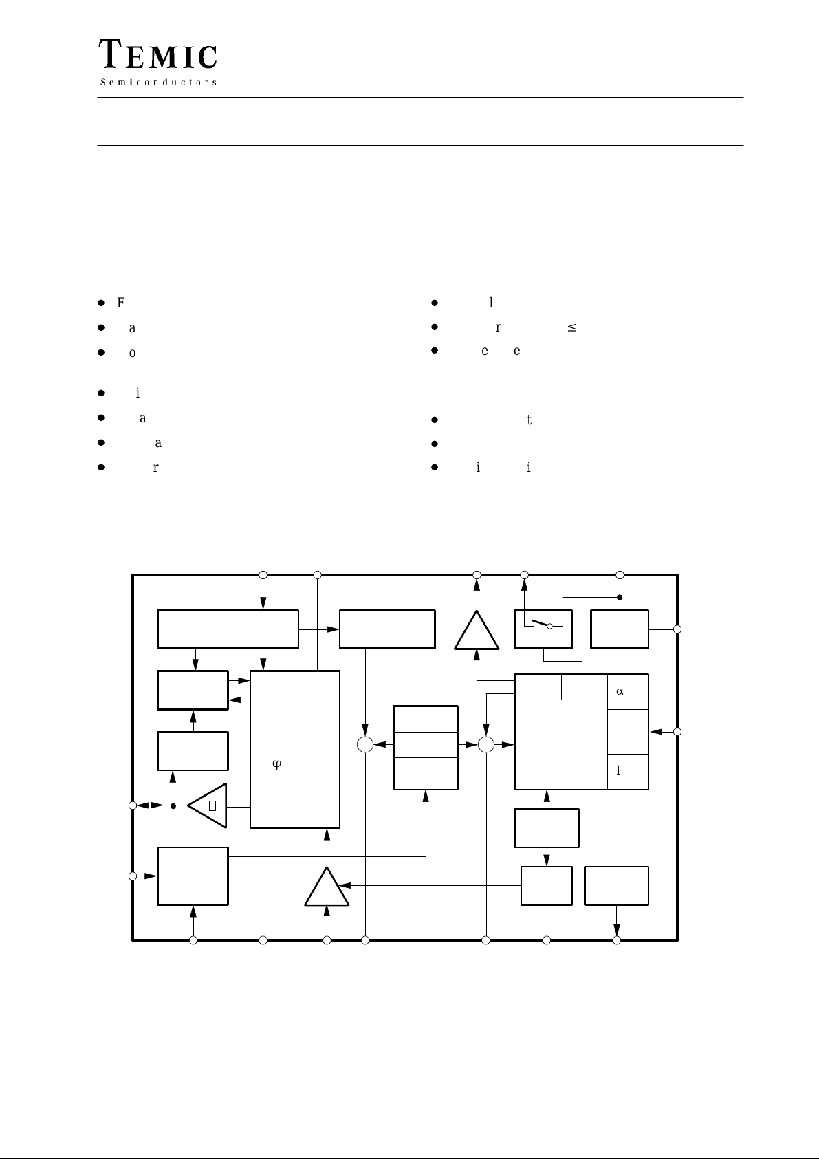
Block Diagram
96 11646
Limiting
detector
Automatic
retriggering
Current
detector
16
Pulse
output
Load
1
current
detector
15
Voltage
detector
control unit
Phase
ö
= f (V
Level
shift
14 13 12
Overload
Mains voltage
)
4
compensation
Output
–
12
Full wave
rectifier
High load
+
monitoring
100% 70%
Programmable
overload
protection
Voltage
Soft
start
11
Supply
voltage
a
max
Auto–
start
I
max
Reference
voltage
10
GND
A
B
9
C
2
3 5 67 8
TELEFUNKEN Semiconductors
Rev . A1, 28-May-96
4
Figure 1. Block diagram
1 (12)
Page 2
U2010B
C
1
m
22 F
Mode
B
C
A
1
S
3
D
1
D
/2 W
W
18 k
LED
BYT51K
8
R
1
R
a
2
R
W
470 k
max
W
330 k
10
GND
S
V
Overload
14 13 12 11
15
Supply
voltage
High load
compensation
Mains voltage
Voltage
detector
detector
Limiting
9
B
A
max
a
100% 70%
Output
Automatic
retriggering
C
max
I
Auto–
start
overload
protection
Programmable
+
2
rectifier
1
Full wave
–
)
4
= f (V
Phase
ö
control unit
Current
detector
Voltage
monitoring
Reference
Soft
Level
Load
current
96 11647
voltage
m
2
C
4.7 F
start
threshold
Overload
11
W
R
1 M
5
C
m
m
0.1 F
0.15 F
C
shift
3 5 67 8
24
detector
3
C
10 nF
1
P
4
7
C
Set point
W
50 k
10
R
m
1 F
W
R78.2 k
W
100 k
Load current
compensation
Load
230 V ~
TIC
226
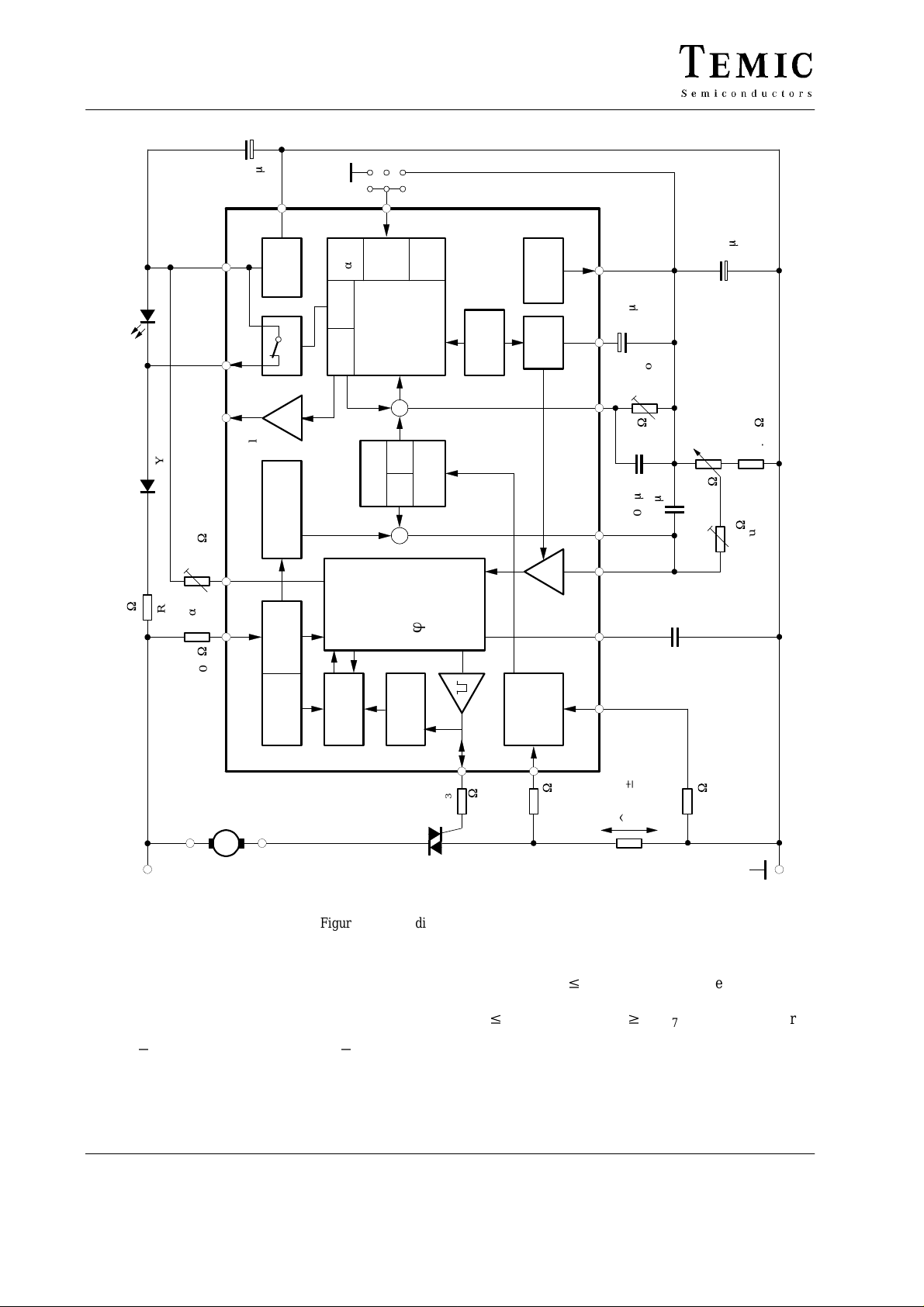
Figure 2. Block diagram with external circuit
General Description
Mains Supply
The U2010B contains voltage limiting and can be
connected with the mains supply via D
voltage * between Pin 10 and Pin 11 * is smoothed
.
by C
1
2 (12)
and R1. Supply
1
16
W
3
R
180
In the case of V
1
W
4
R
3.3 k
v (70% of overload threshold voltage),
6
$
= 250 mV
(R6)
^
V
6
R
W
5
R
3.3 k
Pins 11 and 12 are connected internally whereby
v 1.2 V. When V6 w V
V
sat
flows across D
.
3
, the supply current
T70
TELEFUNKEN Semiconductors
Rev . A1, 28-May-96
Page 3
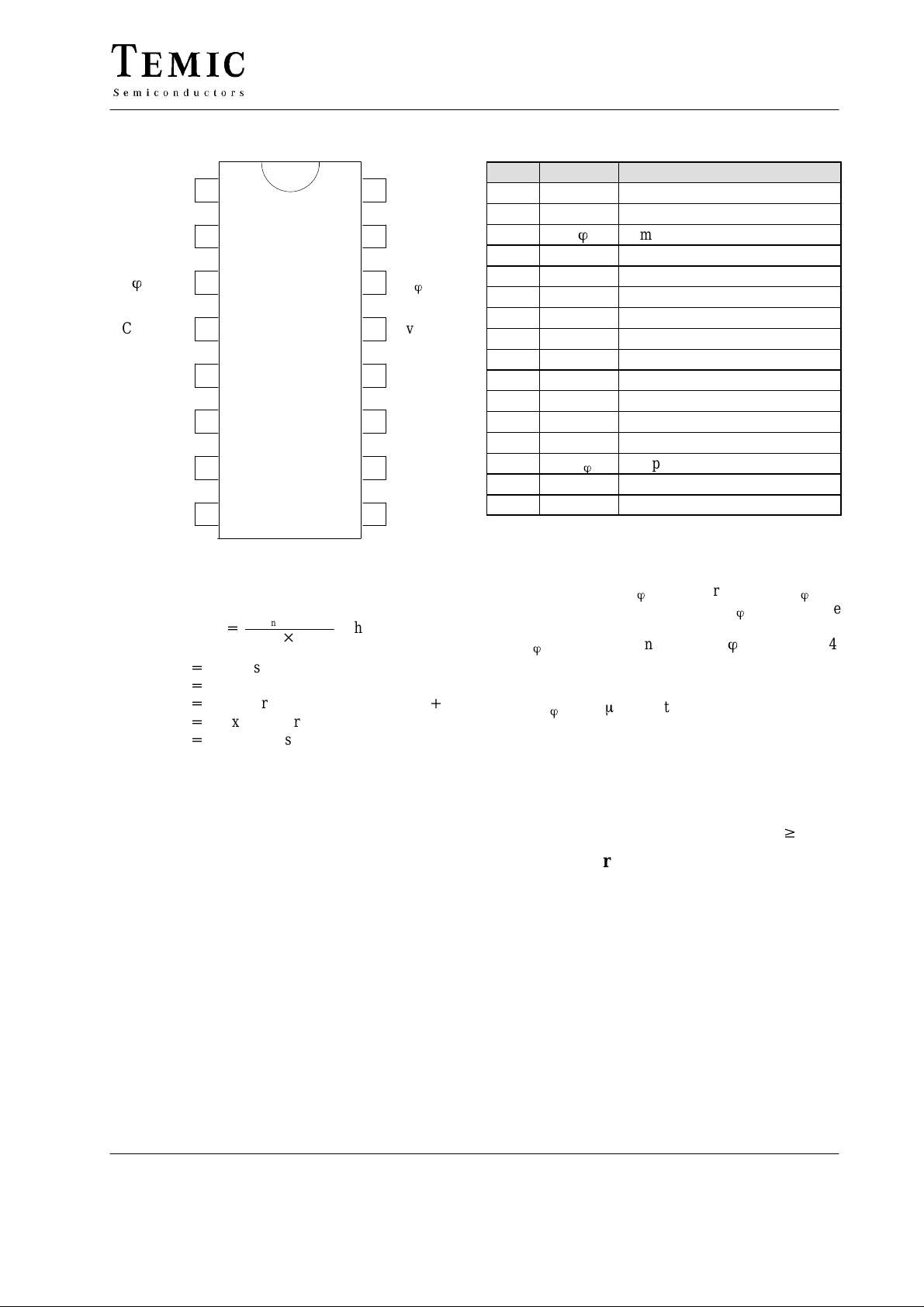
Pin Description
I
sense
I
sense
C
ö
Control
Comp.
I
Load
C
soft
V
Ref
1
2
3
4
5
6
7
8
16
15
14
13
12
11
10
9
Output
V
Sync.
V
R
ö
Overload
High load
V
S
GND
Mode
U2010B
Pin Symbol Function
1 I
2 I
sense
sense
3 C
4 Control Control input
5 Comp. Compensation output
6 I
7 C
8 V
Load
soft
Ref
9 Mode Mode selection
10 GND Ground
11 V
12 High load High load indication
13 Overload Overload indication
14 V
15 V
R
Sync.
16 Output Trigger output
Load current sensing
Load current sensing
ö
Ramp voltage
Load current limitation
Soft start
Reference voltage
Supply voltage
S
Ramp current adjust
ö
Voltage synchronization
95 11406
Series resistance R1 can be calculated as follows:
V
–V
V
mains
V
Smax
I
tot
I
Smax
I
x
R
+
+
+
+
+
1max
mains
+
Mains supply voltage
Maximum supply voltage
Total current consumption = I
Maximum current consumption of the IC
Current consumption of the
2 I
Smax
tot
whereas
Smax
)I
x
external components
Voltage Monitoring
As the voltage is built up, uncontrolled output pulses are
avoided by internal voltage monitoring. Apart from that
all the latches in the circuit (phase control, load limit
regulation) are reset and the soft-start capacitor is short
circuited. This guarantees a specified start-up behavior
each time the supply voltage is switched on or after short
interruptions of the mains supply. Soft-start is initiated
after the supply voltage has been built up. This behavior
guarantees a gentle start-up for the motor and automatically ensures the optimum run-up time.
Phase Control
The function of the phase control is largely identical to the
well known IC family U211B. The phase angle of the
trigger pulse is derived by comparing the ramp voltage V
which is mains synchronized by the voltage detector with
the set value on the control input, Pin 4. The slope of the
ramp is determined by C
charging current can be varied using R
maximum phase angle, α
using R
(minimum current flow angle
ö
and its charging current Iö. The
ö
can also be adjusted by
max,
at Pin 14. The
ö
ö
) see figure 4.
min
When the potential on Pin 3 reaches the set point level of
Pin 4, a trigger pulse width, t
value of C
(tp = 9 ms/nF). At the same time, a latch is set
ö
, is determined from the
p
with the output pulse, as long as the automatic
retriggering has not been activated, then no more pulses
can be generated in that half cycle. Control input at Pin 4
(with respect to Pin 10) has an active range from
to –1 V. When V4 = V8, then the phase angle is at its
V
8
maximum, α
The minimum phase angle, α
i.e., the current flow angle is minimum.
max,
is set with V4 w –1 V.
min,
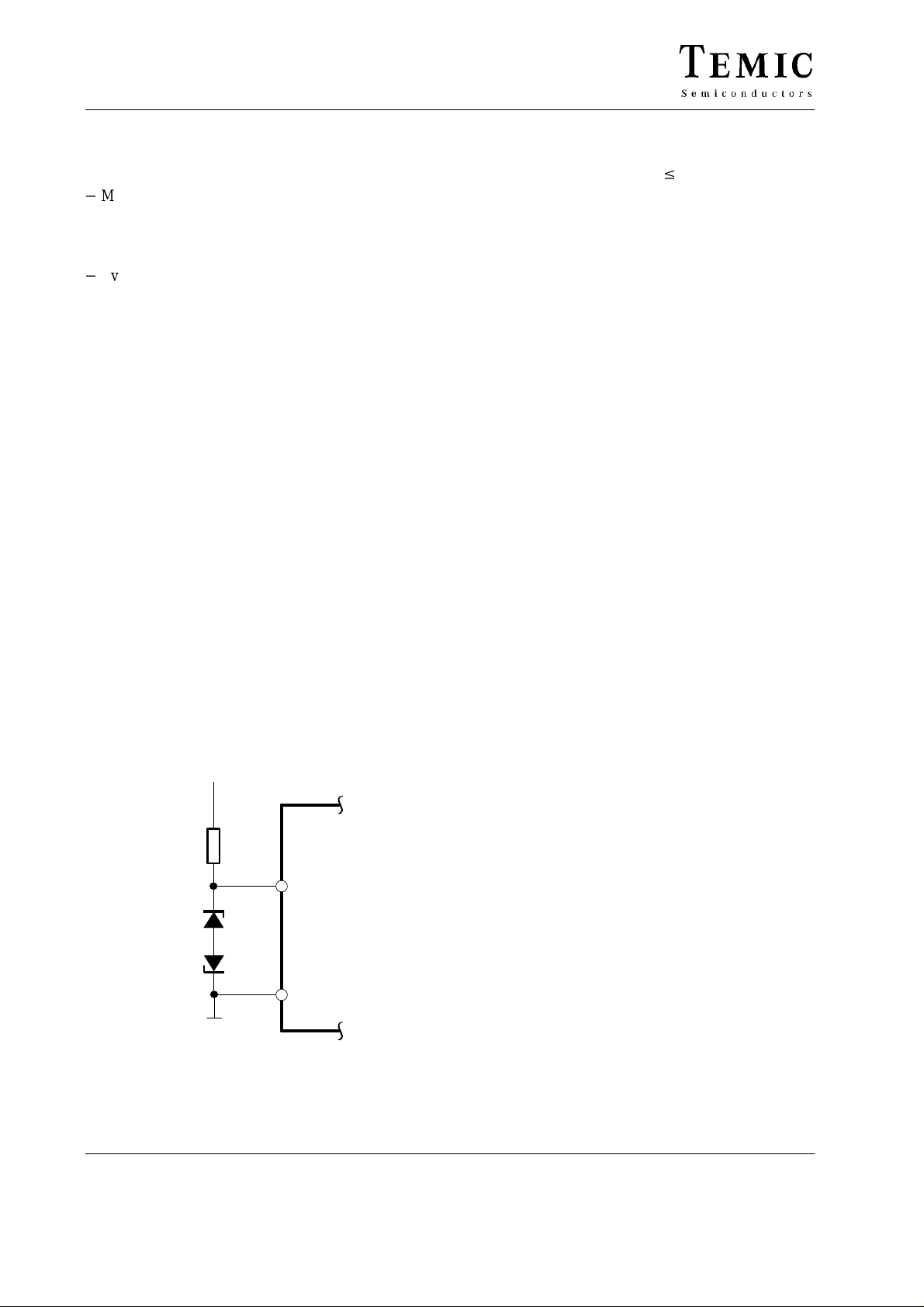
Automatic Retriggering
The current-detector circuit monitors the state of the triac
after triggering by measuring the voltage drop at the triac
gate. A current flow through the triac is recognized, when
the voltage drop exceeds a thres hold level of typ. 40 mV.
If the triac is quenched within the relevant half-wave after
triggering; for example owing to low load currents before
or after the zero crossing of current wave or; for commutator motors, owing to brush lifters. Then the automatic
retriggering circuit ensures immediate retriggering, if
necessary with a high repetition rate, t
3
remains reliably triggered.
, until the triac
pp/tp
TELEFUNKEN Semiconductors
Rev . A1, 28-May-96
3 (12)
Page 4
U2010B
Current Synchronization
Current synchronization fulfils two functions:
*
Monitoring the current flow after triggering.
In case the triac extinguishes again or it does not switch
on, automatic triggering is activated until the
triggering is successful.
*
Avoiding a triggering due to inductive load.
In the case of inductive load operation the current
synchronization ensures that in the new half wave no
pulse is enabled as long as there is a current available
which from the previous half-wave, which flows from
the opposite polarity to the actual supply voltage.
A special feature of the integrated circuit is the
realization of this current synchronization. The device
evaluates the voltage at the pulse output between gate and
reference electrode of the triac. This results in saving
separate current synchronization input with specified
series resistance.
Voltage Synchronization with Mains Voltage
Compensation
The voltage detector synchronizes the reference ramp
with the mains-supply voltage. At the same time, the
mains dependent input current at Pin 15 is shaped and
rectified internally. This current activates the automatic
retriggering and at the same time is available at Pin 5. By
suitable dimensioning, it is possible to attain the specified
compensation effect. Automatic retriggering and mains
voltage compensation are not activated until |V
increases to 8 V. Resistance, R
defines the width of
sync.
the zero voltage cross over pulse, synchronization
current, and hence the mains supply voltage
compensation current.
Mains
96 11648
– 10|
15
If the mains voltage compensation and the automatic
retriggering are not required, both functions can be
suppressed by limiting |V
| v 7 V (figure 3).
15 – 10
Load Current Compensation
The circuit continuously measures the load current as a
voltage drop at resistance R
. The evaluation and use of
6
both half waves results in a quick reaction to load current
change. Due to voltage at resistance R
, there is a
6
difference between both input currents at Pins 1 and 2.
This difference controls the internal current source,
whose positive current values are available at Pins 5
and 6. The output current generated at Pin 5 contains the
difference from the load-current detection and from the
mains-voltage compensation (see figure 1).
The effective control voltage at Pin 4 is the final current
at Pin 5 together with the desired value network. An
increase of mains voltage causes the increase of control
angle α, an increase of load current results in a decrease
in the control angle. This avoiding a decrease in
revolution by increasing the load as well as the increase
of revolution by the increment of mains supply voltage.
Load Current Limitation
The total output load current is available at Pin 6. It
results in a voltage drop across R
of the load current reaches about 70% of the threshold
value (V
) i.e., ca. 4.35 V at Pin 6, it switches the high
T70
load comparator and opens the switch between Pins 11
and 12. By using an LED between these pins, (11 and 12)
a high load indication can be realized.
If the potential at Pin 6 increases to ca. 6.2 V (= V
it switches the overload comparator. The result is
programmable at Pin 9 (operation mode).
. When the potential
11
T100
),
4 (12)
2x
BZX55
C6V2
R
2
15
U2010B
Mode selection:
a) α
(V9 = 0)
max
In this mode of operation, after V
threshold V
, Pin 13 switches to –V
T100
has reached the
6
(Pin 11) and
S
Pin 6 to GND (Pin 10). A soft-start capacitor is then
shorted and the control angle is switched to α
max
.
This position is maintained until the supply voltage
is switched off. The motor can be started again with
10
soft-start function when the power is switched on
again. As the overload condition switches Pin 13 to
Pin 11, it is possible to set in a smaller control angle,
, by connecting a further resistance between
α
max
Figure 3.
Pins 13 and 14.
TELEFUNKEN Semiconductors
Rev . A1, 28-May-96
Page 5

U2010B
b) Auto start (Pin 9 * open)
The circuit behaves as written under α
max
with the exception that Pin 6 is not connected to
GND. If the value of V
threshold value (V
decreases to 25% of the
6
), the circuit becomes active
T25
again with soft-start.
(V9 = 0),
c) I
max
When V
maximum value i.e. V
to Pin 8 (V
without soft-start capacitor discharging at Pin 7.
With this mode of operation, direct load current
control (I
shown in figure 18.
Absolute Maximum Ratings
Reference point Pin 10, unless otherwise specified
Parameters Symbol Value Unit
Sink current Pin 11 –I
t
v
10 m
s –i
Sync. currents Pin 15
v
10 m
t
s
Phase control
Control voltage Pins 4 and 8 –V
Input current Pin 4
Charging current Pin 14 – I
Soft-start
Input voltage Pins 7 and 8 –V
Pulse output
Input voltage Pin 16 +V
Reference voltage source
Output current Pin 8 I
t
v
10 m
s 30
Load current sensing
Input currents Pins 1 and 2
Input voltages Pins 5 and 6 – V
Overload output Pin 13 I
High-load output Pin 12
v
10 m
t
s
Storage temperature range T
Junction temperature range T
Ambient temperature range T
"
"
(V9 = V8)
S
s
I
syncV
i
syncV
I
"
I
I
max
ϕ
I
I
–V
I
0
"
I
i
i
L
I
L
stg
j
amb
has attained the overload threshold
6
) through the resistance R (= 2 kW)
Ref
) is possible. A recommended circuit is
max
= V
6
; Pin 13 is switched
T100
30 mA
100
5
mA
20
0 – V
500
8
V
m
A
0.5 mA
0 – V
2
V
11
8
V
V
10 mA
1 mA
0 – V
8
V
1 mA
30
mA
100
*
40 to )125
125
*
10 to )100
C
C
C
Thermal Resistance
Parameters Symbol Value Unit
Junction ambient DIP16
SO16 on p.c.
SO16 on ceramic
TELEFUNKEN Semiconductors
Rev . A1, 28-May-96
R
thJA
120
K/W
180
100
5 (12)
Page 6

U2010B
Electrical Characteristics
VS + –13 V, T
= 25°C, reference point Pin 10, unless otherwise specified
amb
Parameters Test Conditions / Pins Symbol Min. T yp. Max. Unit
Supply Pin 11
Supply voltage limitation –I
Current requirement –V
= 3.5 mA
S
= 30 mA
–I
S
S
= 13.0 V
(Pins 1, 2, 8 and 15 open)
Reference voltage source Pin 8
Reference voltage I
Temperature coefficient I
= 10 A
L
= 2.5 mA
I
L
= 2.5 mA
S
= 10 A
I
S
–V
TC
Voltage monitoring Pin 11
Turn-on threshold –V
Phase control – synchronization Pin 15
Input current V oltage sync.
Voltage limitation
"
I
= 2 mA
L
Input current Current sync. Pin 16
"
"
"
Reference ramp, figure 4
Charging current Pin 14 –I
Start voltage Pin 3 –V
Temperature coefficient of
start voltage
Pin 3 TC
Final voltage Pin 3 –V
Rϕ − reference voltage I
Temperature coefficient I
Pulse output current V
Output pulse width V
=
ϕ
ϕ
I
ϕ
C
Α Pins 14 and 11 V
=
Α Pin 14
=
Α
= – 1.2 V, figure 5, Pin 16 I
16
= V
S
limit,
= 3.3 nF, figure 6, Pin 16
3
TC
Automatic retriggering
Repetition rate I15 w 150 A t
Threshold voltage Pin 16
Soft start, figure 7 and 8 Pin 7
Starting current V
Final current V
= V
7
8
= –1V –I
7–10
Discharge current +I
Output current Pin 4 +I
Supply voltage compensation, figure 9 Pin 15
Transfer gain I15/ I
5
Pin 15/5
(Pins 1 and 2 open)
Output offset current V
Load current detection, R
1 =
(R6)
R
2
= V
= V5 = 0
15
= 3 k, V15 = 0, V
= V6 = V
5
figure 10
8,
Transfer gain I5/150 mV, I6/150 mV G
Output offset currents Pin 5, Pin 6 - 8 –I
Reference voltage I1, I2 = 100 A Pins 1 and 2 –V
Shunt voltage amplitude see figure 2
"
–V
–I
VRef
I
syncV
V
syncV
I
syncI
t
pp
"
–I
G
"
V
S
Ref
Son
ϕ
max
min
R
VR
0
p
V
0
0
0
0
i
I
I
0
Ref
(R6)
S
14.5
14.6
16.5
16.8
V
3.2 mA
8.6
8.4
8.9
8.8
–0.004
9.2
9.1
V
%/K
+0.006
11.3 12.3 V
0.15 2 mA
8.0 8.5 9.0 V
3 30
1 100
A
A
1.85 1.95 2.05 V
R
ϕ
0.96 1.02 1.10 V
ϕ
–0.003 %/K
(V8"
200 mV)
0.03
%/K
0.06
100 125 150 mA
30
3 5 7.5 t
I
20 60 mV
5 10 15
15 25 40
s
p
A
A
0.5 mA
0.2 2 mA
14 17 20
0
2
0.28 0.32 0.37
0 3 6
A/mV
A
A
300 400 mV
250 mV
6 (12)
TELEFUNKEN Semiconductors
Rev . A1, 28-May-96
Page 7

Load current limitation, Pin 6-8, figs. 11 to 14
High load switching Threshold V
T70
U2010B
UnitMax.Typ.Min.SymbolTest Conditions / PinsParameters
V
T70
4 4.35 4.7 V
Overload switching Threshold V
Restart switching Threshold V
T100
T25
V
T100
V
Input current Enquiry mode I
Output impedance Switching mode R
Programming input, figure 2, Pin 9
Input voltage - auto-start Pin 9 open –V
Input current V9 = 0 (
V
High load output, V
, figure 12, I12 = –3 mA, Pin 11-12
T70
Saturation voltages V
V
Overload output, V
, V9 = open or V9 = V10, fig. 13
T100
Leakage current V
V
Saturation voltages V
I
a
)
max
= V8 (I
9
6-8
v
6-8
w
6-8
v
= (V11+1)V Pin 13 I
13
6-8
w
= 10 mA Pins 11-13 V
13
V
V
V
V
max
T70
T70
T25
T100
)
,
–I
V
V
Output current, max. load V9 = V8, fig. 13 Pin 13 I
Leakage current V
V
6
T100
v
Pin 13 I
Output impedance Open collector
Saturation voltage V
V
V
6
T100
w
V
6-8
I
13
T100
w
= 10 mA Pin 13 V
Pin 13 R
,
13–8
T25
I
9
sat
lim
lkg
sat
13
lkg
5.8 6.2 6.6 V
1.25 1.55 1.85 V
i
0
9
9
2 4 8 k
3.8 4.3 4.7 V
5
5
0.5
7.0
10
10
0.75
7.4
1
20
20
1.0
7.8
0.5
mA
W
mA
V
mA
0.1 V
1 mA
4
0
2 4 8 k
mA
W
100 mV
250
10 nF
6.8 nF
4.7 nF 3.3 nF 2.2 nF
Rö ( kW )96 11797
33 nF
200
°
a
150
100
Phase angle ( )
50
0
0 200 400 600 800 1000
Figure 4.
TELEFUNKEN Semiconductors
Rev . A1, 28-May-96
C
/ t
ö
= 1.5 nF
GT
I ( mA )
95 10338
120
100
80
60
40
20
0
0 200 400 600 800
RGT ( W )
Figure 5.
Pulse Output
V
=–1.2V
GT
1000
7 (12)
Page 8

U2010B
m
p
t ( s )
95 10339
m
7
I ( A )
400
Output Pulse Width
D
t
/DCö=9ms/nF
p
300
200
100
0
01020
Cö = ( nF )
Figure 6.
50
Soft Start
V
=–13V
S
40
V
6=V8
30
Reference Point Pin 8
20
0
40
80
m
5
I ( A )
120
Mains Supply
Compensation
160
Pins 1 and 2 open
V
=–13V
s
30
200
–2 –1 0 1
95 10342
Reference Point
Pin 10
2
I15 ( mA )
Figure 9.
200
Load Current
Detection
V
160
6=VRef=V8
VS=–13V
V
=0V
15=V10
120
m
5
I ( A )
80
Reference Point
Pin 8
95 10340
7
V ( V )
95 10341
10
0
0 2.5 5.0 7.5
V7 ( V )
Figure 7.
12
10
1mF
8
2.2mF 4.7mF
6
4
2
0
02468
Reference Point Pin 8
Cö=10mF
Soft Start
V
=–13V
S
V
6=V8
t ( s )
Figure 8.
40
0
10
95 10343
–400 –200 0 200
V
( mV )
(R6)
400
Figure 10.
20
Load Current limitation:
Auto Start Operation
V
=–13V
16
S
Pin 9 open
Reference Points: V
=Pin 10, V6=Pin 8
13
12
13–10
–V ( V )
8
4
V
10
95 10344
02468
0
T25
V
T100
10
V
( V )
6–8
Figure 11.
8 (12)
TELEFUNKEN Semiconductors
Rev . A1, 28-May-96
Page 9

U2010B
11–12
V ( V )
95 10345
13–10
–V ( V )
10
High Load Output ( 70% )
I
=–3mA
12
8
6
4
Reference Point Pin 8
2
0
012 34
V6 ( V )
Figure 12.
12
Load Current limitation:
Current Control Operation
10
VS=–13V
8
V
9=V8
Reference Points:
V
=Pin 10
6
13
V
=Pin 8
6
4
V
T70
56
10
Power Dissipation at Series Resistance R
1
8
6
V
P ( W )
4
2
0
7
95 10348
010203040
R1 ( kW )
50
Figure 15.
10
Power Dissipation at Series Resistance
8
6
V
P ( W )
4
95 10346
13–10
V ( V )
95 10347
2
V
0
T100
02468
t ( s )
Figure 13.
20
Load Current limitation:
V
=–13V
S
16
V
9=V10
Reference Points: V13=Pin 10, V6=Pin 8
a
max
Operation
12
8
4
V
0
T100
02468
V
( V )
6–8
Figure 14.
2
0
10
95 10350
03 6 912
IS ( mA )
15
Figure 16.
100
80
W
60
1max
R (k )
40
20
0
10
95 10349
02468
Max. Series Resistance
V
=230V
X
M
IS ( mA )
10
Figure 17.
TELEFUNKEN Semiconductors
Rev . A1, 28-May-96
9 (12)
Page 10

U2010B
Application Circuit
1
m
C
3
D
1
D
/2 W
W
18 k
96 11649
LED
BYT51K
8
R
W
470 k
1
R
22 F
max
a
W
1 M
2
R
10
S
V
Overload
max
a
9
R
14 13 12 11
15
W
GND
Supply
voltage
High load
compensation
Mains voltage
Voltage
detector
A
100% 70%
max
a
B
C
A
1
S
9
B
Auto–
start
overload
Programmable
+
2
Output
1
–
Phase
control unit
C
max
I
protection
rectifier
Full wave
4
= f(V )
ö
12
W
R
BC308
220 k
T1
2
D
1N4148
voltage
Reference
m
2
C
4.7 F
Soft
Voltage
monitoring
start
11
R
threshold
Overload
W
1 M
5
C
m
m
0.1 F
0.15 F
shift
Level
3 5 67 8
3
C
1
P
4
C
10 nF
6
C
7
C
Set point
W
50 k
10
R
m
1 F
m
1 F
R
W
100 k
13
W
100 k
W
R78.2 k
Load current
compensation
230 V ~
10 (12)
330 k
24
Load
detector
Limiting
Automatic
retriggering
Current
detector
16
W
3
R
Load
TIC
226
180
L
current
detector
1
250 mV
W
4
R
3.3 k
"
=
(R6)
^
V
6
R
W
5
R
3.3 k
N
Figure 18.
TELEFUNKEN Semiconductors
Rev . A1, 28-May-96
Page 11

Dimensions in mm
Package: DIP16
U2010B
94 9128
Package: SO16
94 8875
TELEFUNKEN Semiconductors
Rev . A1, 28-May-96
11 (12)
Page 12

U2010B
Ozone Depleting Substances Policy Statement
It is the policy of TEMIC TELEFUNKEN microelectronic GmbH to
1. Meet all present and future national and international statutory requirements.
2. Regularly and continuously improve the performance of our products, processes, distribution and operating systems
with respect to their impact on the health and safety of our employees and the public, as well as their impact on
the environment.
It is particular concern to control or eliminate releases of those substances into the atmosphere which are known as
ozone depleting substances (ODSs).
The Montreal Protocol ( 1987) and its London Amendments (1990 ) intend to severely restrict the use of ODSs and
forbid their use within the next ten years. Various national and international initiatives are pressing for an earlier ban
on these substances.
TEMIC TELEFUNKEN microelectronic GmbH semiconductor division has been able to use its policy of
continuous improvements to eliminate the use of ODSs listed in the following documents.
1. Annex A, B and list of transitional substances of the Montreal Protocol and the London Amendments respectively
2. Class I and II ozone depleting substances in the Clean Air Act Amendments of 1990 by the Environmental
Protection Agency (EPA) in the USA
3. Council Decision 88/540/EEC and 91/690/EEC Annex A, B and C (transitional substances) respectively.
TEMIC can certify that our semiconductors are not manufactured with ozone depleting substances and do not contain
such substances.
We reserve the right to make changes to improve technical design and may do so without further notice.
Parameters can vary in different applications. All operating parameters must be validated for each customer
application by the customer. Should the buyer use TEMIC products for any unintended or unauthorized
application, the buyer shall indemnify TEMIC against all claims, costs, damages, and expenses, arising out of,
directly or indirectly, any claim of personal damage, injury or death associated with such unintended or
unauthorized use.
12 (12)
TEMIC TELEFUNKEN microelectronic GmbH, P.O.B. 3535, D-74025 Heilbronn, Germany
Telephone: 49 (0)7131 67 2831, Fax number: 49 (0)7131 67 2423
TELEFUNKEN Semiconductors
Rev . A1, 28-May-96
 Loading...