

Datasheet TS68020VF16, TS68020MRB-C25, TS68020MRB-C20, TS68020MRB-C16, TS68020MR25 Datasheet (ATMEL)
...
1
Features
• Object Code Compatible with Earlier TS68000 Microprocessors
• Addressing Mode Extensions for Enhanced Support of High Level Languages
• New Bit Field Data Type Accelerates Bit-oriented Application, i.e. Video Graphics
• Fast on-chip Instruction Cache Speed Instructions and Improves Bus Bandwidth
• Co-processor Interface to Companion 32-bit Peripherals: TS68881 and TS68882
Floating Point Co-processors
• Pipelined Architecture with High Degree of Internal Parallelism Allowing Multiple
Instructions to be Executed Concurrently
• High Performance Asynchronous Bus in Non-multiplexed and Full 32 Bits
• Dynamic Bus Sizing Efficiently Supports 8-, 16-, 32-bit Memories and Peripherals
• Full Support of Virtual Memory and Virtual Machine
• Sixteen 32-bit General-purpose Data and Address Registers
• Two 32-bit Supervisor Stack Pointers and 5 Special Purpose Control Registers
• 18 Addressing Modes and 7 Data Types
• 4-Gbyte Direct Addressing Range
• Processor Speed: 16.67 MHz - 20 MHz - 25 MHz
• Power Supply: 5.0 V
DC
± 10%
Description
The TS68020 is the first full 32-bit implementation of the TS68000 family of microprocessors. Using HCMOS technology, the TS68020 is implemented with 32-bit registers
and data paths, 32-bit addresses, a rich instruction set, and versatile addressing
modes.
Screening/Quality
This product is manufactured in full compliance with either:
• MIL-STD-883 (class B)
• DESC 5962 - 860320
• or according to Atmel standards
See “Ordering Information” on page 43.
Pin connection: see page 3.
Rsuffix
PGA 114
Ceramic Pin Grid Array
Fsuffix
CQFP 132
Ceramic Quad Flat Pack
HCMOS 32-bit
Virtual Memory
Microprocessor
TS68020
Rev. 2115A–HIREL–07/0 2
2
TS68020
2115A–HIREL–07/02
Introduction The TS68020 is a high-performance 32-bit microprocessor. It is the first microprocessor
to have evolved from a 16-bit machine to a full 32-bit machine that provides 32-bit
address and data buses as well as 32-bit internal structures. Many techniques were utilized to improve performance and at the same time maintain compatibility with other
processors of the TS68000 Family. Among the improvements are new addressing
modes which better support high-level language structures, an expanded instruction set
which provides 32-bit operations for the limited cases not supported by the TS68000
and several new instructions which support new data types. For special-purpose applications when a general-purpose processor alone is not adequate, a co-processor
interface is provided.
The TS68020 is a high-performance microprocessor implemented in HCMOS, low
power, small geometry process. This process allows CMOS and HMOS (high density
NMOS) gates to be combined on the same device. CMOS structures are used where
speed and low power is required, and HMOS structures are used where minimum silicon area is desired. This technology enables the TS68020 to be very fast while
consuming less power (less than 1.5 watts) and still have a reasonably small die size. It
utilizes about 190.000 transistors, 103.000 of which are actually implemented. The
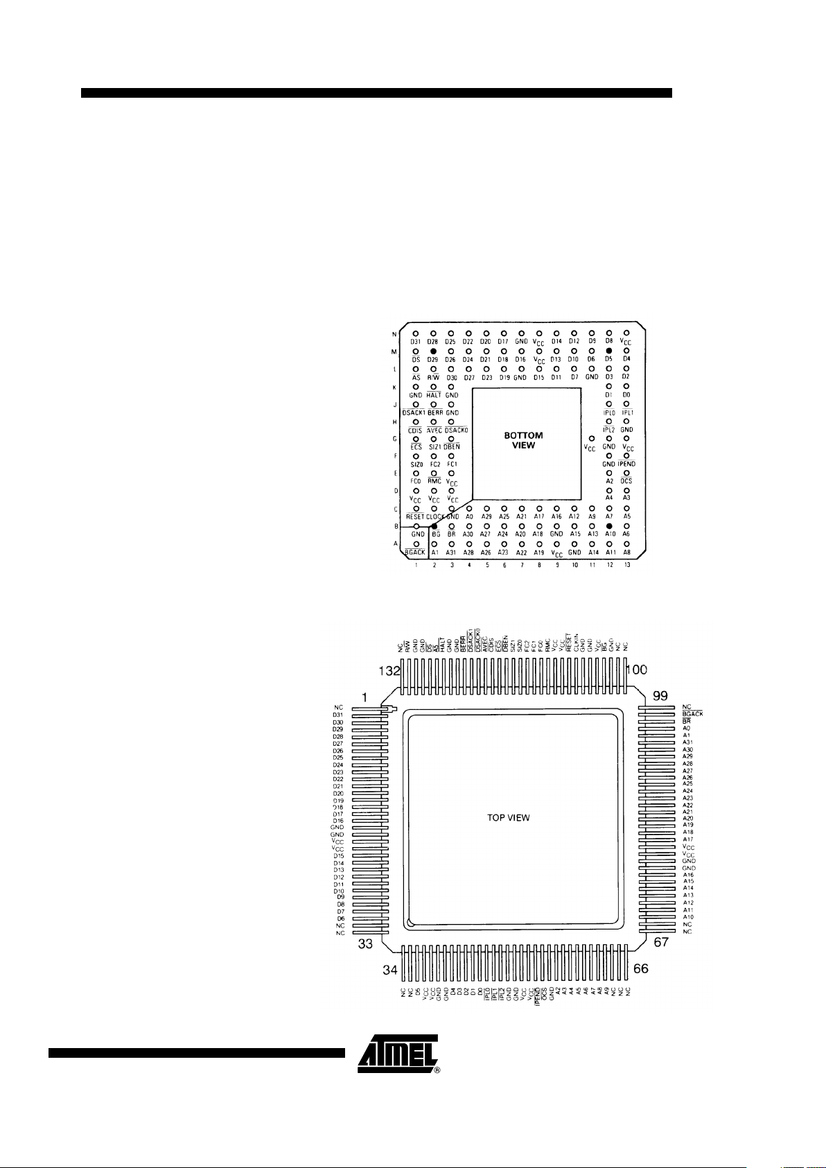
package is a pin-grid array (PGA) with 114 pins, arranged 13 pins on a side with a
depopulated center and 132 pins ceramic quad flat pack.
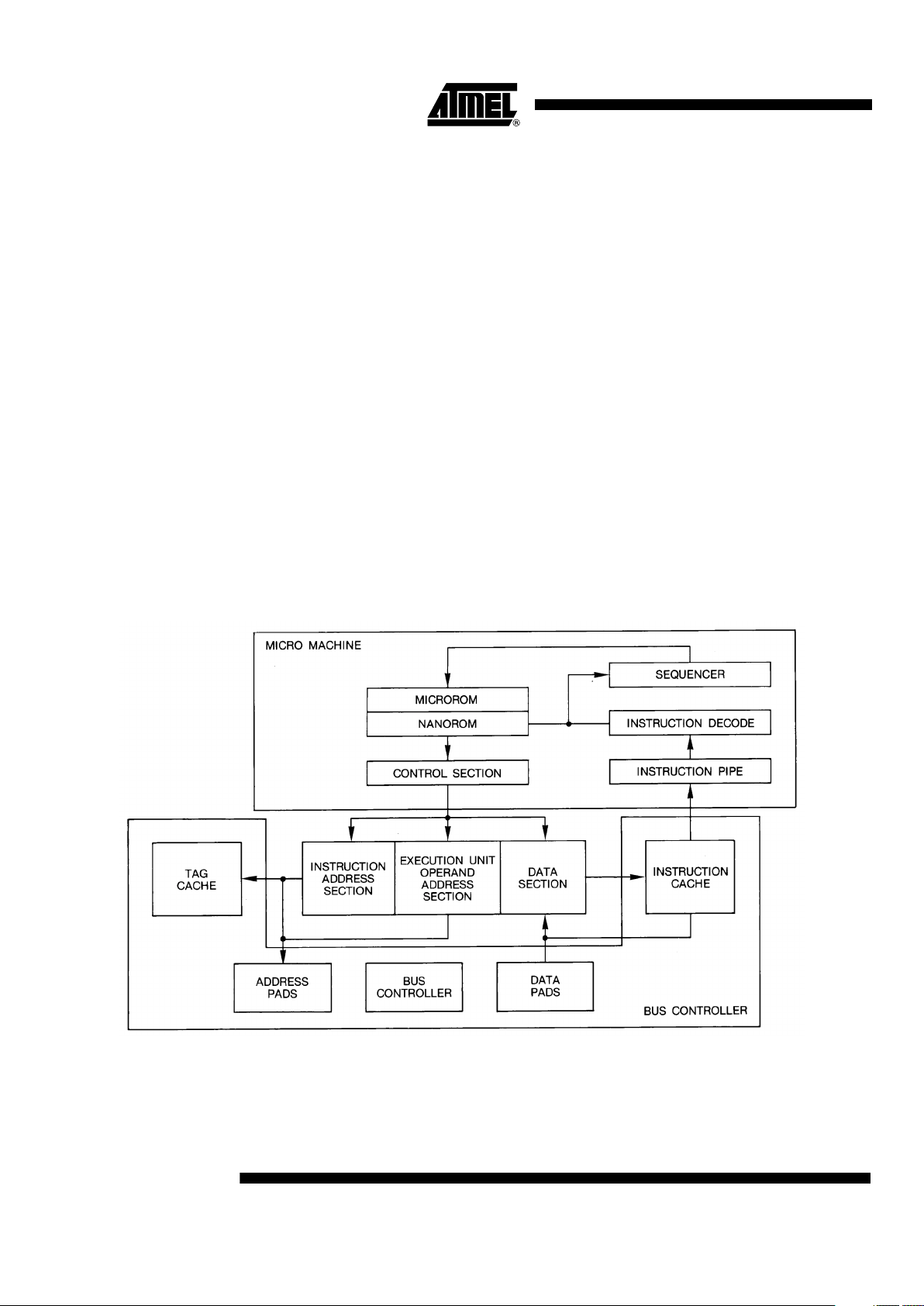
Figure 1 is a block diagram of the TS68020. The processor can be divided into two main
sections: the bus controller and the micromachine. This division reflects the autonomy
with which the sections operate.
Figure 1. TS68020 Block Diagram
The bus controller consists of the address and data pads and multiplexers required to
support dynamic bus sizing, a macro bus controller which schedules the bus cycles on
the basis of priority with two state machines (one to control the bus cycles for operated
accesses and the other to control the bus cycles for instruction accesses), and the
instruction cache with its associated control.
3
TS68020
2115A–HIREL–07/02
The micromachine consists of an execution unit, nanorom and microrom storage, an
instruction decoder, an instruction pipe, and associated control sections. The execution
unit consists of an address section, an operand address section, and a data section.
Microcode control is provided by a modified two-level store of microrom and nanorom.
Programmed logical arrays (PLAs) are used to provide instruction decode and sequencing information. The instruction pipe and other individual control sections provide the
secondary decode of instructions and generated the actual control signals that result in
the decoding and interpretation of nanorom and micorom information.
Figure 2. PGA Terminal Designation
Figure 3. CQFP Terminal Designation
4
TS68020
2115A–HIREL–07/02
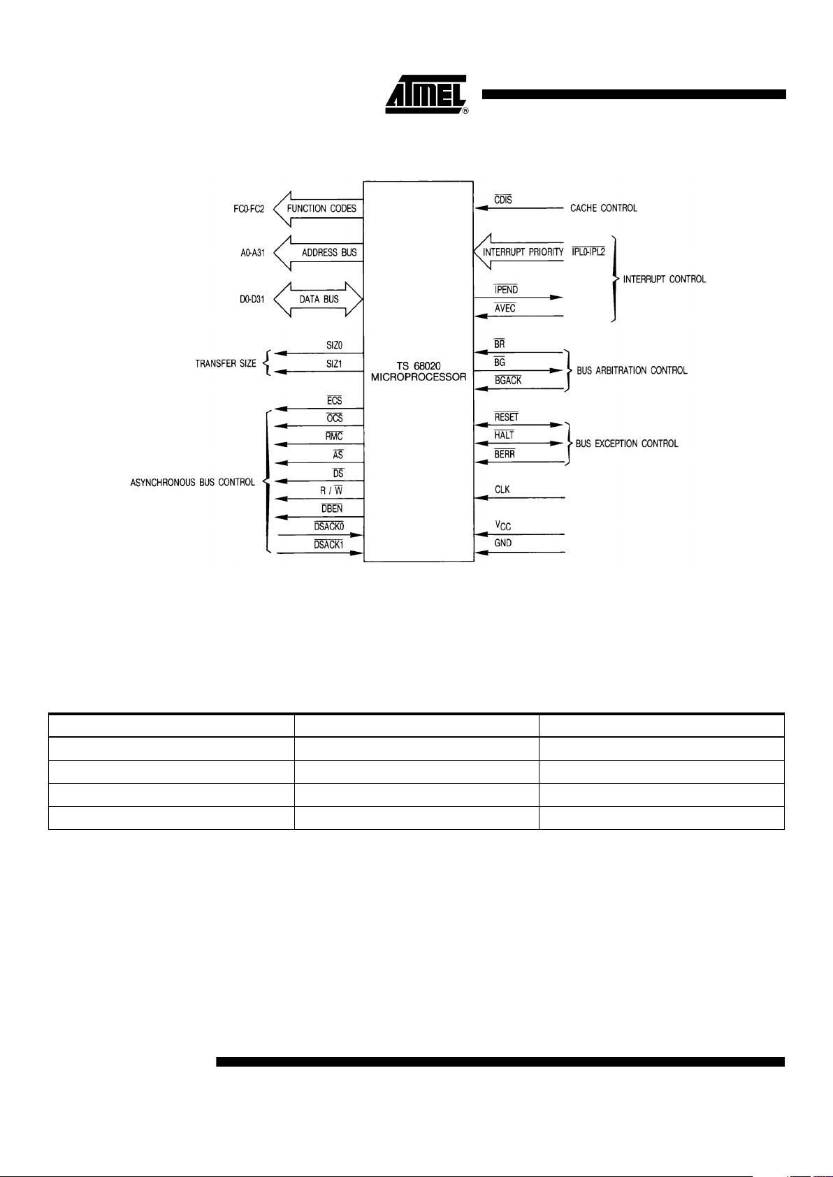
Figure 4. Functional Signal Groups
Signal Description Figure 4 illustrates the functional signal groups and Table 1 lists the signals and their
function.
The V
CC
and GND pins are separated into four groups to provide individual power supply connections for the address bus buffers, data bus buffers, and all other output
buffers and internal logic.
Group V
CC
GND
Address Bus A9, D3 A10, B9,C3, F12
Data Bus M8, N8, N13 L7, L11, N7, K3
Logic D1, D2, E3, G11, G13 G12, H13, J3, K1
Clock — B1
5
TS68020
2115A–HIREL–07/02
Table 1 . Signal Index
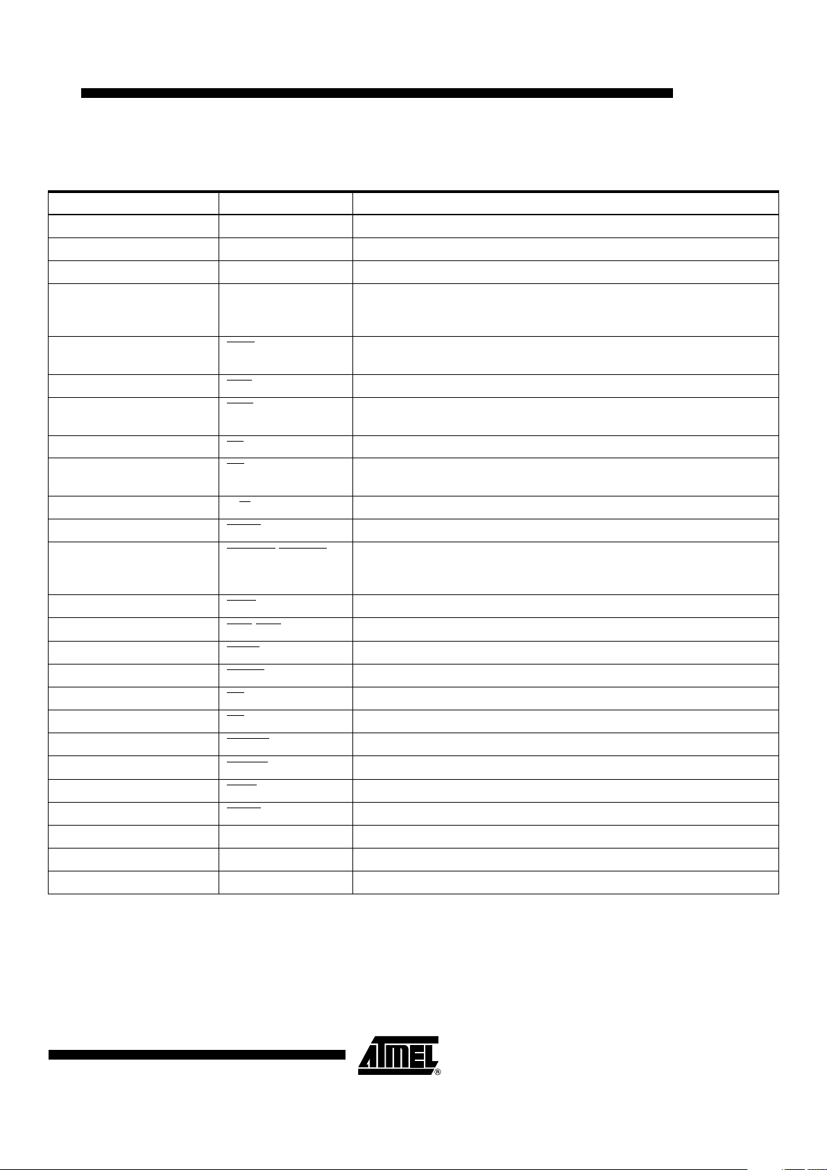
Signal Name Mnemonic Function
Address Bus A0-A31 32-bit Address Bus Used to address any of 4, 294, 967, 296 bytes.
Data Bus D0-D31 32-bit Data Bus Used to Transfer 8, 16, 24 or 32 bits of Data Per Bus Cycle.
Function Codes FC0-FC2 3-bit Function Case Used to Identify the Address Space of Each Bus Cycle.
Size SIZ0/SIZ1 Indicates the Number of Bytes Remaining to be Transferred for this Cycle.
These Signals, Together with A0 And A1, Define the Active Sections of the
Data Bus.
Read-Modify-Write Cycle RMC
Provides an Indicator that the Current Bus Cycle is Part of an Indivisiblereadmodify-write Operation.
External Cycle Start ECS
Provides an Indication that a Bus Cycle is Beginning.
Operand Cycle Start OCS
Identical Operation to that of ECS Except that OCS Is Asserted Only During
the First Bus Cycle of an Operand Transfer.
Address Strobe AS
Indicates that a Valid Address is on The Bus.
Data Strobe DS
Indicates that Valid Data is to be Placed on the Data Bus by an External
Device or has been Laced on the Data Bus by the TS68020.
Read/Write R/W
Defines the Bus Transfer as an MPU Read or Write.
Data Buffer Enable DBEN
Provides an Enable Signal for External Data Buffers.
Data Transfer and Size
Acknowledge
DSACK0
/DSACK1 Bus Response Signals that Indicate the Requested Data Transfer Operation
is Completed. In Addition, these Two Lines Indicate the Size of the External
Bus Port on a Cycle-by-cycle Basis.
Cache Disable CDIS
Dynamically Disables the On-chip Cache to Assist Emulator Support.
Interrupt Priority Level IPL0
-IPL2 Provides an Encoded Interrupt Level to the Processor.
Autovector AVEC
Requests an Autovector During an Interrupt Acknowledge Cycle.
Interrupt Pending IPEND
Indicates that an Interrupt is Pending.
Bus Request BR
Indicates that an External Device Requires Bus Mastership.
Bus Grant BG
Indicates that an External Device may Assume Bus Mastership.
Bus Grant Acknowledge BGACK
Indicates that an External Device has Assumed Bus Mastership.
Reset RESET
System Reset.
Halt HALT
Indicates that the Processor Should Suspend Bus Activity.
Bus Error BERR
Indicates an Invalid or Illegal Bus Operation is Being Attempted.
Clock CLK Clock Input to the Processor.
Power Supply V
CC
+5-volt ± 10% Power Supply.
Ground GND Ground Connection.

6
TS68020
2115A–HIREL–07/02
Detailed
Specifications
Scope
This drawing describes the specific requirements for the microprocessor 68020,
16.67 MHz, 20 MHz and 25 MHz, in compliance with the MIL-STD-883 class B.
Applicable
Documents
MIL-STD-883 • MIL-STD-883: Test Methods and Procedures for Electronics
• MIL-PRF-38535 appendix A: General Specifications for Microcircuits
• Desc Drawing 5962 - 860320xxx
Requirements
General The microcircuits are in accordance with the applicable document and as specified
herein.
Design and Construction
Terminal Connections Depending on the package, the terminal connections shall be as shown in Figure 2 and
Figure 3.
Lead Material and Finish Lead material and finish shall be any option of MIL-STD-1835.
Package The macrocircuits are packages in hermetically sealed ceramic packages which are
conform to case outlines of MIL-STD-1835 (when defined):
• 114-pin SQ.PGA UP PAE Outline
• 132-pin Ceramic Quad Flat Pack CQFP
The precise case outlines are described on Figure 23 and Figure 24.
7
TS68020
2115A–HIREL–07/02
Electrical Characteristics
Note: 1. Load network number 1 to 4 as specified (Table 7) gives the maximum loading of the relevant output.
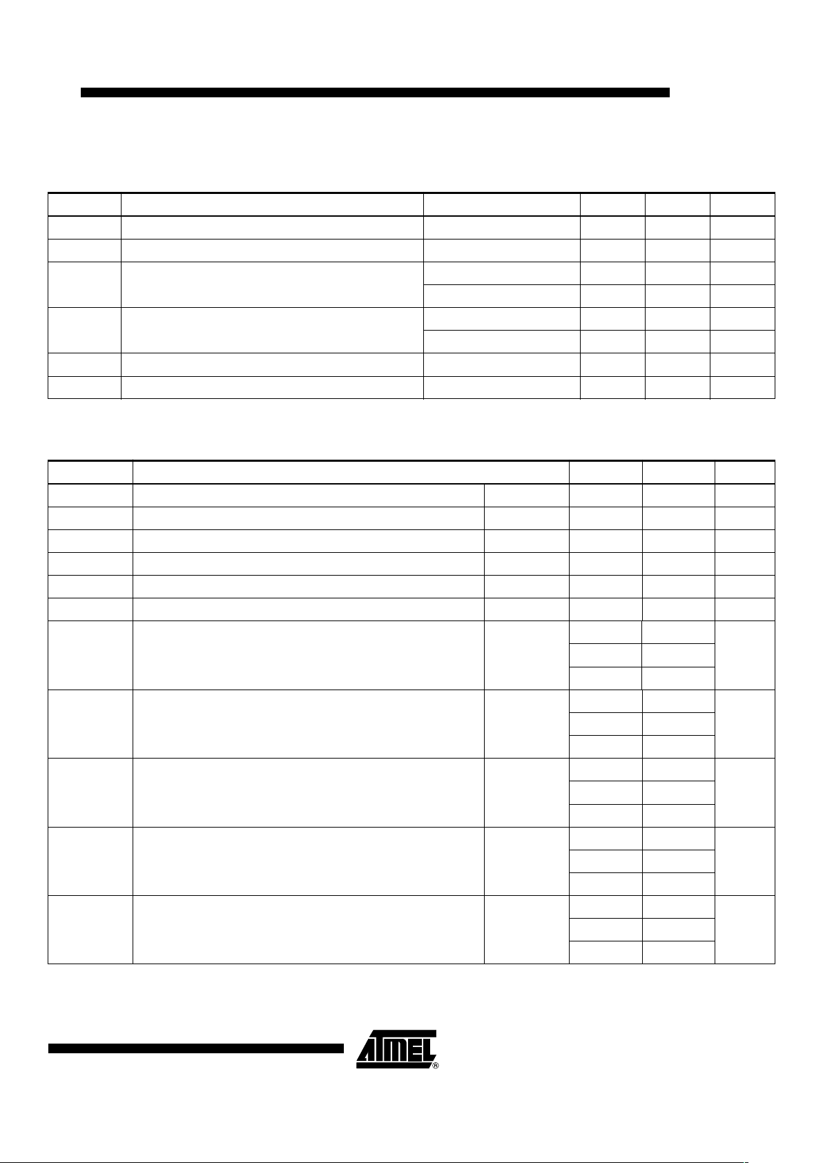
Table 2 . Absolute Maximum Ratings
Symbol Parameter Test Conditions Min Max Unit
V
CC
Supply Voltage -0.3 +7.0 V
V
I
Input Voltage -0.5 +7.0 V
P
dmax
Max Power Dissipation
T
case
=-55°C2.0W
T
case
= +125°C1.9W
T
case
Operating Temperature
M Suffix -55 +125
°C
V Suffix -40 +85
°C
T
stg
Storage Temperature -55 +150 °C
T
leads
Lead Temperature Max 5 Sec. Soldering +270 °C
Table 3 . Recommended Condition of Use
Unless otherwise stated, all voltages are referenced to the reference terminal (see Table 1).
Symbol Parameter Min Max Unit
V
CC
Supply Voltage 4.5 5.5 V
V
IL
Low Level Input Voltage -0.3 0.5 V
V
IH
High Level Input Voltage 2.4 5.25 V
T
case
Operating Temperature -55 +125 °C
R
L
Value of Output Load Resistance
(1)
Ω
C
L
Output Loading Capacitance
(1)
pF
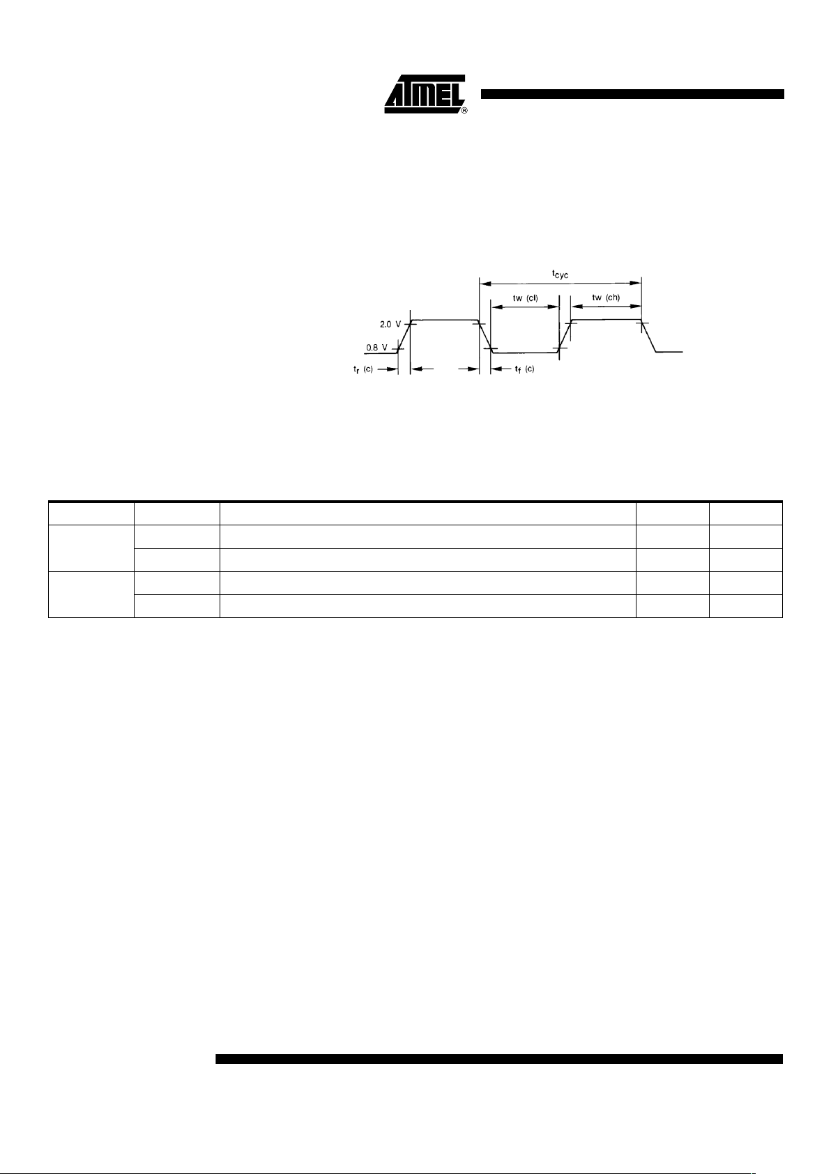
t
r
(c)–tf(c) Clock Rise Time (See Figure 5)
68020-16 5
ns68020-20 5
68020-25 4
f
c
Clock Frequency (See Figure 5)
68020-16 8 16.67
MHz68020-20 12.5 20
68020-25 12.5 25
t
cyc
CycleTime(seeFigure5)
68020-16 60 125
ns68020-20 50 80
68020-25 40 80
t
W
(CL) Clock Pulse Width Low (See Figure 5)
68020-16 24 95
ns68020-20 20 54
68020-25 19 61
t
W
(CH) ClockPulseWidthHigh(SeeFigure5)
68020-16 24 95
ns68020-20 20 50
68020-25 19 61
8
TS68020
2115A–HIREL–07/02
This device contains protective circuitry against damage due to high static voltages or
electrical fields; however, it is advised that normal precautions be taken to avoid application of any voltages higher than maximum-rated voltages to this high-impedance circuit.
Reliability of operation is enhanced if unused inputs are tied to an appropriate logic voltage level (e.g., either GND or V
CC
).
Figure 5. Clock Input Timing Diagram
Note: Timing measurements are referenced to and from a low voltage of 0.8V and a high volt-
age of 2.0V, unless otherwise noted. The voltage swing through this range should start
outside and pass through the range such that the rise or fall will be linear between 0.8V
and 2.0V.
Power Considerations The average chip-junction temperature, T
J,
in °C can be obtained from:
T
J=TA
+(PD· θJA)(1)
T
A
= Ambient Temperature, °C
θ
JA
= Package Thermal Resistance, Junction-to-Ambient, °C/W
P
D=PINT+PI/O
P
INT=ICC·VCC
, Watts — Chip Internal Power
P
I/O
= Power Dissipation on Input and Output Pins — User Determined
For most applications P
I/O<PINT
and can be neglected.
An approximate relationship between P
D
and TJ(if P
I/O
is neglected) is:
P
D
=K+(TJ+ 273) (2)
Solving equations (1) and (2) for K gives:
K=P
D
·(TA+273)+θJA·P
D
2
(3)
where K is a constant pertaining to the particular part K can be determined from equation (3) by measuring P
D
(at equilibrium) for a known TA. Using this value of K, the
values of P
D
and TJcan be obtained by solving equations (1) and (2) iterativley for any
value of T
A
.
Table 4 . Thermal Characteristics at 25°C
Package Symbol Parameter Value Unit
PGA 114
θ
JA
Thermal Resistance - Ceramic Junction to Ambient 26 °C/W
θ
JC
Thermal Resistance - Ceramic Junction to Case 5 ° C/W
CQFP 132
θ
JA
Thermal Resistance - Ceramic Junction to Ambient 34 °C/W
θ
JC
Thermal Resistance - Ceramic Junction to Case 2 ° C/W

9
TS68020
2115A–HIREL–07/02
The total thermal resistance of a package (θJA) can be separated into two components,
θ
JC
and θCA, representing the barrier to heat flow from the semiconductor junction to the
package (case), surface (θ
JC
) and from the case to the outside ambient (θCA). These
terms are related by the equation:
θ
JA
= θJC= θ
CA
(4)
θ
JC
is device related and cannot be influenced by the user. However, θCAis user dependent and can be minimized by such thermal management techniques as heat sinks,
ambient air cooling and thermal convection. Thus, good thermal management on the
part of the user can significantly reduce θ
CA
so that θJAapproximately equals θJC. Substi-
tution of θ
JC
for θJAin equation (1) will result in a lower semiconductor junction
temperature.
Mechanical and
Environment
The microcircuits shall meet all mechanical environmental requirements of MIL-STD883 for class B devices.
Marking The document where are defined the marking are identified in the related reference doc-
uments. Each microcircuit are legible and permanently marked with the following
information as minimum:
• ATMEL Logo
• Manufacturer’s Part Number
• Class B Identification
• Date-code of Inspection Lot
• ESD Identifier if Available
• Country of Manufacturing
Quality Conformance
Inspection
DESC/MIL-STD-883 Is in accordance with MIL-M-38510 and method 5005 of MIL-STD-883. Group A and B
inspections are performed on each production lot. Group C and D inspections are performed on a periodical basis.
Electrical
Characteristics
General Requirements All static and dynamic electrical characteristics specified and the relevant measurement
conditions are given below.
(last issue on request to our marketing services).
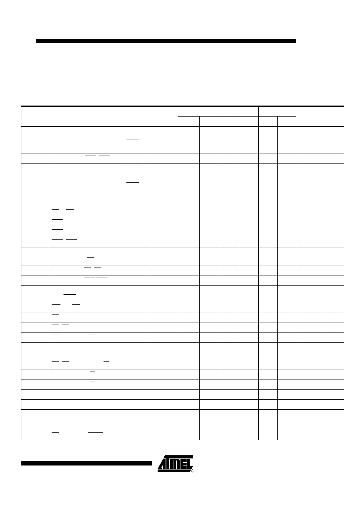
Table 5: Static electrical characteristics for all electrical variants.
Table 6: Dynamic electrical characteristics for 68020-16 (16.67 MHz), 68020-20 (20
MHz) and 68020-25 (25 MHz).
For static characteristics, test methods refer to “Test Conditions Specific to the Device”
on page 14 hereafter of this specification (Table 7).
10
TS68020
2115A–HIREL–07/02
For dynamic characteristics (Table 6), test methods refer to IEC 748-2 method, where
existing.
Indication of “min.” or “max.” in the column “test temperature” means minimum or maximum operating temperature.
.
Table 5 . Static Characteristics. VCC=5.0VDC± 10%; GND = 0VDC;Tc= -55/+125°Cor-40/+85°C (Figure 4 to Figure 8)
Symbol Parameter Condition Min Max Units
I
CC
Maximum Supply Current VCC=5.5V
T
case
-55°Cto+25°C
333 mA
I
CC
Maximum Supply Current VCC=5.5V
T
case
=125°C
207 mA
V
IH
High Level Input Voltage VO= 0.5V or 2.5
V
CC
= 4.5V to 5.5V
2.0 V
CC
V
V
IL
Low Level Input Voltage VO= 0.5V or 2.4V
V
CC
= 4.5V to 5.5V
-0.5 0.8 V
V
OH
High Level Output Voltage
All Outputs
IOH= 400 µA 2.4 V
V
OL
Low Level Output Voltage
Outputs A0-A31, FC0-FC2, D0-D31, SIZ0-SIZ1, BG
IOL=3.2mA
Load Circuit as
Figure 8
R=1.22kΩ
0.5 V
V
OL
Low Level Output Voltage
Outputs AS
,DS,RMC,R/W, DBEN, IPEND
IOL=5.3mA
Load Circuit as
Figure 8
R=740Ω
0.5 V
V
OL
Low Level Output Voltage
Outputs ECS
,OCS
IOL=2.0mA
Load Circuit as
Figure 8
R=2kΩ
0.5 V
V
OL
Low Level Output Voltage
Outputs HALT
, RESET
IOL= 10.7 mA
Load Circuit as Figure 6
and Figure 7
0.5 V
|I
IN
| Input Leakage Current (High and Low State) -0.5V ≤ VIN≤ VCC(Max) 2.5 µA
|I
OHZ
| High level leakage current at three-state outputs
Outputs A0-A31, AS
, DBEN,DS, D0-D31, R/W, FC0-FC2,
RMC
,SIZ0-SIZ1
V
OH
=2.4V 2.5 µA
|I
OLZ
| Low Level Leakage Current at Three-state Outputs
Outputs A0-A31, AS
, DBEN,DS,D0-D31R/W, FC0-FC2, RMC,
SIZ0-SIZ1
V
OL
= 0.5V 2.5 µA
I
OS
Output Short-circuit Current
(Any Output)
VCC=5.5V
V
O
=0V
(Pulsed. Duration 1 ms
Duty Cycle 10:1)
200 mA
11
TS68020
2115A–HIREL–07/02
Dynamic (Switching)
Characteristics
The limits and values given in this section apply over the full case temperature range 55°C to +125°CandV
CC
in the range 4.5V to 5.5V VIL=0.5VandVIH=2.4V(Seealso
note 12 and 13). The INTERVAL numbers refer to the timing diagrams. See Figure 5,
Figure 9 and Figure 12.
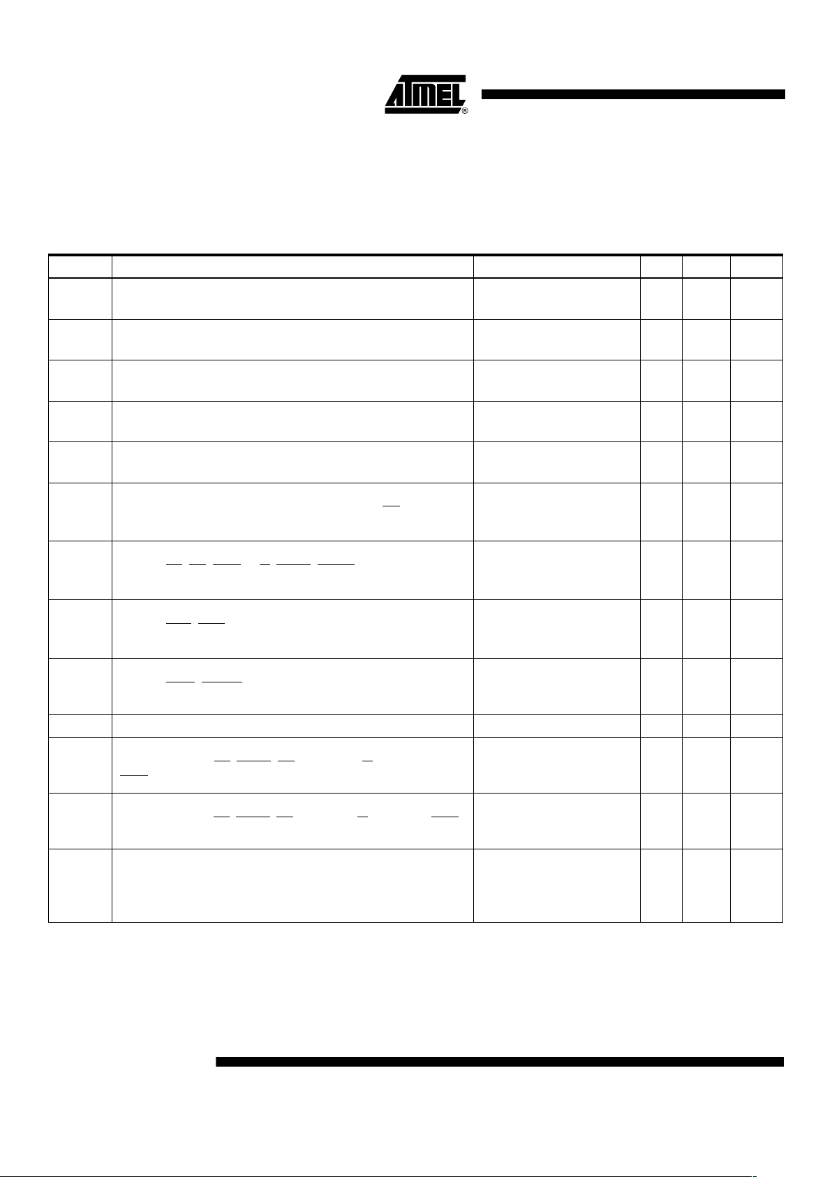
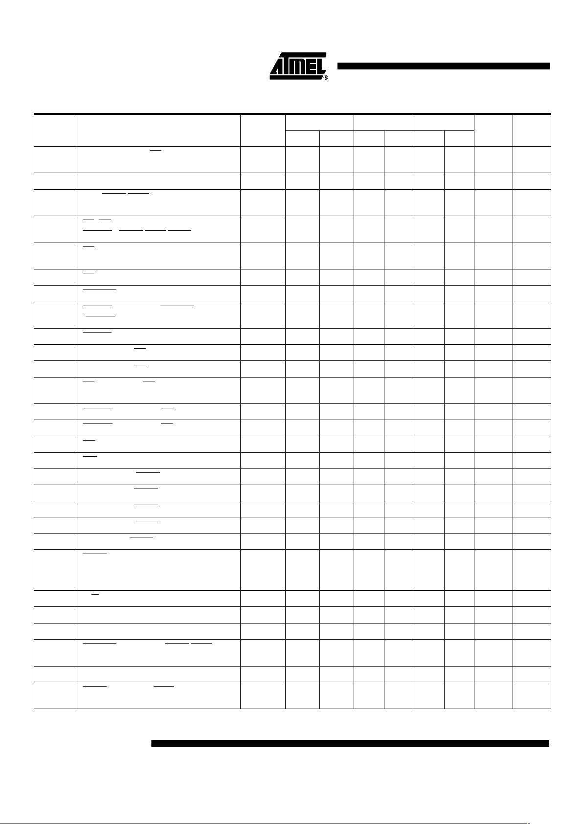
Table 6 . Dynamic Electrical Characteristics
Symbol Parameter
Interval
Number
68020-16 68020-20 68020-25
Unit NotesMin Max Min Max Min Max
t
CPW
Clock Pulse Width 2 , 3 24 95 20 54 19 61 ns
t
CHAV
Clock High to Address/FC/Size/RMC
Valid
6 0 30 025025 ns
t
CHEV
Clock High to ECS,OCSAsserted 6A 0 20015012ns
t
CHAZX
Clock High to Address/Data/FC/RMC/
Size High Impedance
7 0 60 050040 ns
(11)
t
CHAZn
Clock High to Address/FC/Size/RMC
Invalid
80 0 0 ns
t
CLSA
Clock Low to AS,DSAsserted 9 3 30 325318 ns
t
STSA
AS to DS Assertion (Read)(Skew) 9A -15 15 -10 10 -10 10 ns
(1)
t
ECSA
ECS Width Asserted 10 20 15 15 ns
t
OCSA
OCS Width Asserted 10A 20 15 15 ns
t
EOCSN
ECS,OCSWidth Negated 10B 15 10 5 ns
(11)
t
AVSA
Address/FC/Size/RMC ValidtoAS
Asserted (and DS Asserted, Read)
11 15 10 6 ns
(6)
t
CLSN
Clock Low to AS,DSNegated 12 0 30 0 25 0 15 ns
t
CLEN
Clock Low to ECS/OCS Negated 12A 0 30 0 25 0 15 ns
t
SNAI
AS,DS Negated to Address/FC/
Size/RMC
Invalid
13 15 10 10 ns
t
SWA
AS (and DS, Read) Width Asserted 14 100 85 70 ns
t
SWAW
DS Width Asserted, Write 14A 40 38 30 ns
t
SN
AS,DSWidth Negated 15 40 38 30 ns
(11)
t
SNSA
DS NegatedtoASAsserted 15A 35 30 25 ns
(8)
t
CSZ
Clock High to AS/DS/R/W/DBEN High
Impedance
16 60 50 40 ns
(11)
t
SNRN
AS,DS Negated to R/W High 17 15 10 10 ns
(6)
t
CHRH
Clock High to R/W High 18 0 30 0 25 0 20 ns
t
CHRL
Clock High to R/W Low 20 0 30 025020 ns
t
RAAA
R/W High to AS Asserted 21 15 10 5 ns
(6)
t
RASA
R/W Low to DS Asserted (Write) 22 75 60 50 ns
(6)
t
CHDO
Clock High to Data Out Valid 23 30 25 25 ns
t
SNDI
AS, DS Negated to Data Out Valid 25 15 10 5 ns
(6)
t
DNDBN
DS NegatedtoDBENNegated (Write) 25A 15 10 5 ns
(9)
12
TS68020
2115A–HIREL–07/02
t
DVS A
Data Out Valid to DS Asserted (Write)
26
26 15 10 5 ns
(6)
t
DICL
Data in Valid to Clock Low (Data Setup) 27 5 5 5 ns
t
BELCL
Late BERR/HALT Asserted to Clock
Low Setup Time
27A 20 15 10 ns
t
SNDN
AS,DS Negated to
DSACK
x/BERR/HALT/AVEC Negated
28 0 80065050ns
t
SNDI
DS Negated to Data On Invalid (Data in
Hold Time)
29 0 0 0 ns
(6)
t
SNDIZ
DS Negated to Data in High Impedance 29A 60 50 40 ns
t
DADI
DSACKx Asserted to Data In Valid 31 50 43 32
(2)(1 1)
t
DADV
DSACK Asserted to DSACKx Val id
(DSACK
Asserted Skew)
31A 15 10 10 ns
(3)(1 1)
t
HRrf
RESET Input Transition Time 32 1.5 1.5 1.5 Clks
t
CLBA
Clock Low to BG Asserted 33 0 30 0 25 0 20 ns
t
CLBN
Clock Low to BG Negated 34 0 30 0 25 0 20 ns
t
BRAGA
BR Asserted to BG Asserted (RMC Not
Asserted)
35 1.5 3.5 1.5 3.5 1.5 3.5 Clks
(11)
t
GAGN
BGACK Asserted to BG Negated 37 1.5 3.5 1.5 3.5 1.5 3.5 Clks
(11)
t
GABRN
BGACK Asserted to BR Negated 37A 0 1.5 0 1.5 0 1.5 Clks
(11)
t
GN
BG Width Negated 39 90 75 60 ns
(11)
t
GA
BG Width Asserted 39A 90 75 60 ns
t
CHDAR
Clock High to DBEN Asserted (Read) 40 0 30 0 25 0 20 ns
t
CLDNR
Clock Low to DBEN Negated (Read) 41 0 30 0 25 0 20 ns
t
CLDAW
Clock Low to DBEN Negated (Read) 42 0 30 0 25 0 20 ns
t
CHDNW
Clock High to DBEN Asserted (Read) 43 0 30 0 25 0 20 ns
t
RADA
R/W Low to DBEN Asserted (Write) 44 15 10 10 ns
(6)
t
DA
DBEN Width Asserted
READ
WRITE
45
60
120
50
100
40
80
ns
ns
(5)
(5)
t
RWA
R/W Width Asserted (Write or Read) 46 150 125 100 ns
t
AIST
Asynchronous Input Setup Time 47A 5 5 5 ns
(11)
t
AIHT
Asynchronous Input Hold Time 47B 15 15 10 ns
(11)
t
DABA
DSACKx Asserted to BERR/HALT
Asserted
48 30 20 18 ns
(4)(1 1)
t
DOCH
Data Out Hold from Clock High 53 0 0 0 ns
t
BNHN
BERR NegatedtoHALTNegated
(Rerun)
000ns
Table 6 . Dynamic Electrical Characteristics (Continued)
Symbol Parameter
Interval
Number
68020-16 68020-20 68020-25
Unit NotesMin Max Min Max Min Max
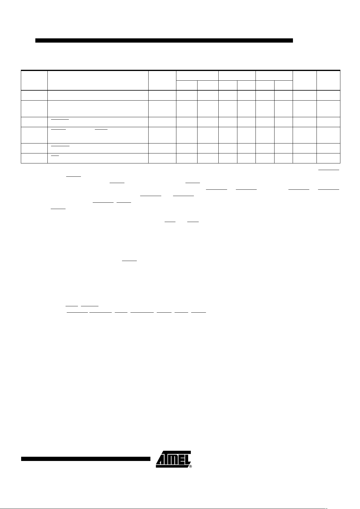
13
TS68020
2115A–HIREL–07/02
Notes: 1. This number can be reduced to 5 nanoseconds if the strobes have equal loads.
2. If the asynchronous setup time (= 47) requirements are satisfied, the DSACKx low to data setup time (= 31) and DSACKx
low to BERR low setup time (= 48) can be ignored. The data must only satisfy the data in to clock low setup time (= 27) for
the following clock cycle, BERR
must only satisfy the late BERR low to clock setup time (= 27) for the following clock cycle.
3. This parameter specifies the maximum allowable skew between DSACK0
to DSACK1 asserted or DSACK1 to DSACK0
asserted pattern = 47 must be met by DSACK0 and DSACK1.
4. In the absence of DSACKx
,BERRis an asynchronous input using the asynchronous input setup time (= 47).
5. DBEN
may stay asserted on consecutive write cycles.
6. Actual value depends on the clock input waveform.
7. This pattern indicates the minimum high time for ECS
and OCS in the event of an internal cache hit followed immediately by
a cache miss or operand cycle.
8. This specification guarantees operations with the 68881 co-processor, and defines a minimum time for DS negated to AS
asserted (= 13A). Without this parameter, incorrect interpretation of = 9A and = 15 would indicate that the 68020 does not
meet 68881 requirements.
9. This pattern allows the systems designer to guarantee data hold times on the output side of data buffers that have output
enable signals generated with DBEN
.
10. Guarantees that an alternate bus master has stopped driving the bus when the 68020 regains control of the bus after an
arbitration sequence.
11. Cannot be tested. Provided for system design purposes only.
12. T
case
=-55°C and +130°C in a Power off condition under Thermal soak for 4 minutes or until thermal equilibrium. Electrical
parameters are tested “instant on” 100 m sec. after power is applied.
13. All outputs unload except for load capacitance. Clock = fmax,
LOW: HALT
, RESET
HIGH: DSACK0,DSACK1, CDIS, IPL0-IPL2, DBEN, AVEC, BERR.
f Frequency of Operation 8.0 16.67 12.5 20.0 12.5 25 MHz
t
RADC
R/W Asserted to Data Bus Impedance
Change
55 30 25 20
(11)
t
HRPW
RESET Pulse Width (Reset Instruction) 56 512 512 512 Clks
(11)
t
BNHN
BERR NegatedtoHALTNegated
(Rerun)
57 0 0 0 ns
(11)
t
GANBD
BGACK Negated to Bus Driven 58 1 1 1 Clks
(10)(11)
t
GNBD
BG NegatedtoBusDriven 59 1 1 1 Clks
(10)(11)
Table 6 . Dynamic Electrical Characteristics (Continued)
Symbol Parameter
Interval
Number
68020-16 68020-20 68020-25
Unit NotesMin Max Min Max Min Max
14
TS68020
2115A–HIREL–07/02
Test Conditions Specific
to the Device
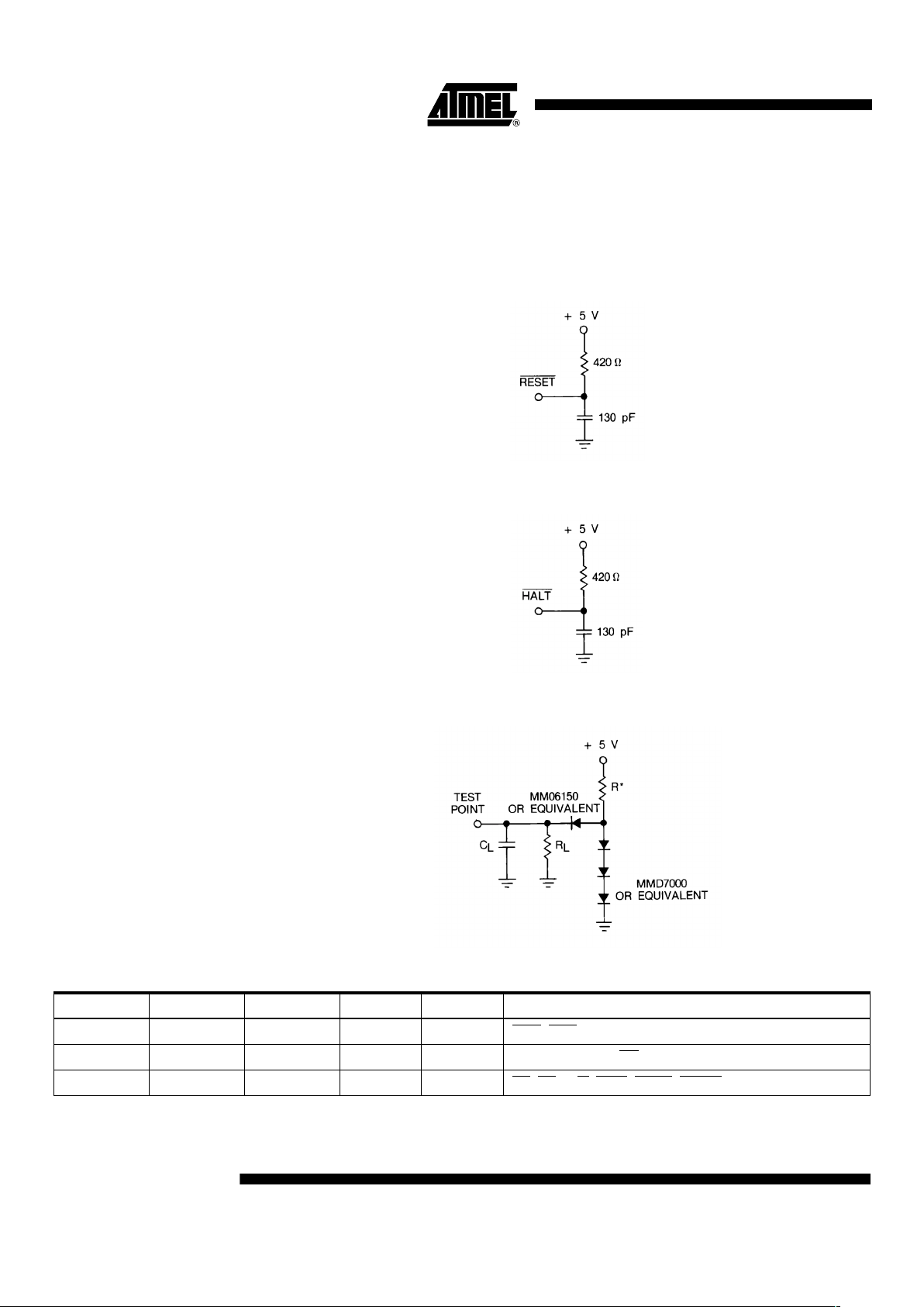
Loading Network The applicable loading network shall be defined in column “Test conditions” of Table 6,
referring to the loading network number as shown in Figure 6, Figure 7, Figure 8 below.
Figure 6. RESET Test Loads
Figure 7. HALT Test Load
Figure 8. Test Load
Note: 1. Equivalent loading may be simulated by the tester.
Table 7 . Load Network
Load NBR Figure R R
L
C
L
Output Application
1 7 2 k 6.0 k 50 pF OCS
,ECS
2 7 1.22 k 6.0 k 130 pF A0-A31, D0-D31, BG, FC0-FC2, SIZ0-SIZ1
3 7 0.74 k 6.0 k 130 pF AS
,DS,R/W,RMC, DBEN, IPEND

15
TS68020
2115A–HIREL–07/02
Time Definitions The times specified in Table 6 as dynamic characteristics are defined in Figure 9 below,
by a reference number given the column “interval N°” of the tables together with the relevant figure number.
Figure 9. Read Cycle Timing Diagram
Note: Timing measurements are referenced to and from a low voltage of 0.8V and a high voltage of 2.0V, unless otherwise noted. The
voltage swing through this range should start outside and pass through the range such that the rise or fall will be linear between
0.8V and 2.0V.

16
TS68020
2115A–HIREL–07/02
Figure 10. Write Cycle Timing Diagram (Continued)
Note: Timing measurements are referenced to and from a low voltage of 0.8V and a high voltage of 2.0V, unless otherwise noted. The
voltage swing thorough this range should start outside and pass through the range such that the rise or fall will be linear
between 0.8V and 2.0V.

17
TS68020
2115A–HIREL–07/02
Figure 11. Bus Arbitration Timing Diagram
Note: Timing measurements are referenced to and from a low voltage of 0.8V and a high voltage of 2.0V, unless otherwise noted. The
voltage swing thorough this range should start outside and pass through the range such that the rise or fall will be linear
between 0.8V and 2.0V.

18
TS68020
2115A–HIREL–07/02
Input and Output Signals for
Dynamic Measurements
AC Electrical Specifications
Definitions
The AC specifications presented consist of output delays, input setup and hold times,
and signal skew times. All signals are specified relative to an appropriate edge of the
TS68020 clock input and, possibly, relative to one or more other signals.
The measurement of the AC specifications is defined by the waveforms in Figure 12. In
order to test the parameters guaranteed by Atmel, inputs must be driven to the voltage
levels specified in Figure 12. Outputs of the TS68020 are specified with minimum and/or
maximum limits, as appropriate, and are measured as shown. Inputs to the TS68020
are specified with minimum and, as appropriate, maximum setup and hold times, and
are measurement as shown. Finally, the measurements for signal-to-signal specification
are also shown.
Note that the testing levels used to verify conformance of the TS68020 to the AC specifications does not affect the guaranteed DC operation of the device as specified in the
DC electrical characteristics.

19
TS68020
2115A–HIREL–07/02
Figure 12. Drive Levels and Test Points for AC Specification
Legend:
A) Maximum Output Delay Specification
B) Minimum Output Hold Time
C) Minimum Input Setup Time Specification
D) Minimum Input Hold Time Specification
E) Signal Valid to Signal Valid Specification (Maximum or Minimum)
F) Signal Valid to Signal Invalid Specification (Maximum or Minimum)
Notes: 1. This output timing is applicable to all parameters specified relative to the rising edge of the clock.
2. This out put timing is applicable to all parameters specified relative to the falling edge of the clock.
3. This input timing is applicable to all parameters specified relative to the falling edge of the clock.
4. This input timing is applicable to all parameters specified relative to the falling edge of the clock.
5. This timing is applicable to all parameters specified relative to the assertion/negation of another signal.

20
TS68020
2115A–HIREL–07/02
Additional Information Additional information shall not be for any inspection purposes.
Power Consideration See Table 4.
Capacitance (Not for
Inspection Purposes
)
Capacitance Derating
Curves
Figure 13 to Figure 18 inclusive show the typical derating conditions which apply. The
capacitance includes any stray capacitance. The graphs may not be linear outside the
range shown.
Figure 13. Address Capacitance Derating Curve
Symbol Parameter Test Conditions Min Unit
C
in
Input Capacitance
V
in
=0VT
amb
=25°C
f=1MHz
20 pF

21
TS68020
2115A–HIREL–07/02
Figure 14. ECS and OCS Capacitance Derating Curve
Figure 15. R/W, FC, SIZ0-SIZ1, and RMC Capacitance Derating Curve

22
TS68020
2115A–HIREL–07/02
Figure 16. DS, AS, IPEND, and BG Capacitance Derating Curve
Figure 17. DBEN Capacitance Derating Curve

23
TS68020
2115A–HIREL–07/02
Figure 18. Data Capacitance Derating Curve
Functional
Description
Description of Registers As shown in the programming models (Figure 19 and Figure 20) the TS68020 has six-
teen 32-bit general-purpose registers, a 32-bit program counter, two 32-bit supervisor
stack pointers, a 16-bit status register, a 32-bit vector base register, two 3-bit alternate
function code registers, and two 32-bit cache handling (address and control) registers.
Registers D0-D7 are used as data registers for bit and bit field (1- to 32-bit), byte (8-bit),
long word (32-bit), and quad word (64-bit) operations. Registers A0-A6 and the user,
interrupt, and master stack pointers are address registers that may be used as software
stack pointers or base address registers. In addition, the address registers may be used
for word and long word operations. All of the 16 (D0-D7, A0-A7) registers may be used
as index registers.
The status register (Figure 21) contains the interrupt priority mask (three bits) as well as
the condition codes: extend (X), negated (N), zero (Z), overflow (V), and carry (C). Additional control bits indicate that the processor is in the trace mode (T1 or T0),
supervisor/user state (S), and master/interrupt state (M).
All microprocessors of the TS68000 Family support instruction tracing (via the T0 status
bit in the TS68020) where each instruction executed is followed by a trap to a userdefined trace routine. The TS68020 adds the capability to trace only the change of flow
instructions (branch, jump, subroutine call and return, etc.) using the T1 status bit.
These features are important for software program development and debug.
The vector base register is used to determine the runtime location of the exception vector table in memory, hence it supports multiple vector tables so each process or task can
properly manage exceptions independent of each other.

24
TS68020
2115A–HIREL–07/02
The TS68000 Family processors distinguish address spaces as supervisor / used and
program/data. These four combinations are specified by the function code pins
(FC0/FC1/FC2) during bus cycles, indication the particular address space. Using the
function codes, the memory sub-system can distinguish between authorized access
(supervisor mode is privileged access) and unauthorized access (user mode may not
have access to supervisor program or data areas). To support the full privileges of the
supervisor, the alternate function code registers allow the supervisor to specify an
access to user program or data areas by preloading the SFC/DFC registers
appropriately.
The cache registers (control — CACR, address — CAAR) allow software manipulation
of the on-chip instruction cache. Control and status accesses to the instruction cache
are provided by the cache control register (CACR), while the cache address register
(CAAR) holds the address for those cache control functions that require an address.
Figure 19. User Programming Model

25
TS68020
2115A–HIREL–07/02
Figure 20. Supervisor Programming Model Supplement
Figure 21. Status Register
Data Types and
Addressing Modes
Seven basic types are supported. These data types are:
•Bits
• Bits Flieds (String of consecutive bits, 1-32 bits long)
• BCD Digits (Packed: 2 digits/byte, Unpacked: 1 digit/byte)
• Byte Integers (8-bit)
• Word Integers (16-bit)
• Long Word Integers (32-bit)
• Quad Word Integers (64-bit)
In addition, operations on other data types, such as memory addresses, status word
data, etc...., are provided in the instruction set. The co-processor mechanism allows
direct support of floating-point data type with the TS68881 and TS68882 floating-point
co-processors, as well as specialized user-defined data types and functions.

26
TS68020
2115A–HIREL–07/02
The 18 addressing modes, shown in Table 8, include nine basic types:
• Register Direct
• Register Indirect
• Register Indirect with Index
• Memory Indirect
• Program Counter Indirect with Displacement
• Program Counter Indirect with Index
• Program Counter Memory Indirect
• Absolute
• Immediate
The register indirect addressing modes support postincrement, predecrement, offset,
and indexing. Programmers find these capabilities particularly useful for handling
advanced data structures common to sophisticated applications and high level languages. The program counter relative mode also has index and offset capabilities;
programmers find that this addressing mode is required to support position-independent
software. In addition to these addressing modes, the TS68020 provides data operand
sizing and scaling; these features provide performance enhancements to the
programmer.
.
Table 8 . TS68020 Addressing Modes
Addressing Modes Syntax
Register Direct
Data Register Direct
Address Register Direct
Dn
An
Register Indirect
Address Register Indirect
Address Register Indirect with Post Increment
Address Register Indirect with Predecrement
Address Register Indirect with Displacement
(An)
(An) +
–(An)
(d
16
An)
Register Indirect with Index
Address Register Indirect with Index (8-bit Displacement)
Address Register Indirect with Index (Base Displacement)
(d
8
,An,Xn)
(bd, An, Xn)
Memory Indirect
Memory Indirect Post-Indexed
Memory Indirect Pre-Indexed
([bd, An], Xn, od)
([bd, An, Xn], od)
Program Counter Indirect with Displacement (d
16
,PC)
Program Counter Indirect with Index
PC Indirect with Index (8-bit Displacement)
PC Indirect with Index (Base Displacement)
(d
8
,PC,Xn)
(bd, PC, Xn)
Program Counter Memory Indirect
PC Memory Indirect Post-Indexed
PC Memory Indirect Pre-Indexed
([bd, PC], Xn, od)
([bd, PC, Xn]), od)

27
TS68020
2115A–HIREL–07/02
Notes: 1. Dn = Data Register, D0-D7.
2. An = Address Register, A0-A7.
3. d
8,d16
= A twos-complement, or sign—extended displacement; added as part of the effective calculation; size is 8 (d8)or16
(d
16
) bits; when omitted assemblers use a value of zero.
4. Xn = Address or data register used as an index register; form is Xn, SIZE*SCALE, where SIZE is.W or.L (indicates index
register size) and SCALE is 1, 2, 4, or 8 (index register is multiplied by SCALE); use of SIZE and/or SCALE is optional.
5. bd = A two-complement base displacement; when present, size can be 16- or 32-bit.
6. od = Outer displacement, added as part of effective address calculation after any memory indirection; use is optional with a
sizeof16-or32-bit.
7. PC = Program Counter.
8. (data) = Immediate value of 8, 16 or 32 bits.
9. () = Effective Address.
10. [ ] = Use as indirect address to long word address.
Absolute
Absolute Short
Absolute Long
xxx.W
xxx.L
Immediate =data
Table 8 . TS68020 Addressing Modes (Continued)
Addressing Modes Syntax

28
TS68020
2115A–HIREL–07/02
Instruction Set Overview The TS68020 instruction set is shown in Table 9. Special emphasis has been given to
the instruction set’s support of structured high-level languages and sophisticated operating systems. Each instruction, with few exceptions, operates on bytes, words, and long
words and most instructions can use any of the 18 addressing modes. Many instruction
extensions have been made on the TS68020 to take advantage of the full 32-bit operation where, on the earlier 68000 Family members, only 8 and 16 bits values were used.
The TS68020 is upward source- and object-level code compatible with the family
because it supports all of the instructions that previous family members offer. Additional
instructions are now provided by the TS68020 in support of its advanced features.
Table 9 . Instruction Set
Mnemonic Description
ABCD
ADD
ADDA
ADDI
ADDQ
ADDX
AND
ANDI
ASL, ASR
Add Decimal with Extend
Add
Add Address
Add Immediate
Add Quick
AddwithExtend
Logical AND
Logical AND Immediate
Arithmetic Shift Left and Right
Bcc
BCHG
BCLR
BFCHG
BFCLR
BFEXTS
BFEXTU
BFFFO
BFINS
BFSET
BFTST
BKPT
BRA
BSET
BSR
BTST
Branch Conditionally
Test Bit and Change
Test Bit and Clear
Test Bit Field and Change
Test Bit Field and Clear
Signed Bit Field Extract
Unsigned Bit Field Extract
Bit Field Find First One
Bit Field Insert
Te st B it F ie ld a nd S et
Te st B it F ie ld
Breakpoint
Branch
Test Bit and Set
Branch to Subroutine
Te st B it

29
TS68020
2115A–HIREL–07/02
CALLM
CAS
CAS2
CHK
CHK2
CLR
CMP
CMPA
CMPI
CMPM
CMP2
Call Module
Compare and Swap Operands
Compare and Swap Dual Operands
Check Register Against Bound
Check Register Against Upper and Lower Bounds
Clear
Compare
Compare Address
Compare Immediate
Compare Memory to Memory
Compare Register Against Upper and Lower Bounds
DBcc
DIVS, DIVSL
DIVU, DIVUL
Test Condition, Decrement and Branch
Signed Divide
Unsigned Divide
EOR
EORI
EXG
EXT, EXTB
Logical Exclusive OR
Logical Exclusive OR Immediate
Exchange Registers
Sign Extend
ILLEGAL Take Illegal Instruction Tape
JMP
JSR
Jump
Jump to Subroutine
LEA
LINK
LSL, LSR
Load Effective Address
Link and Allocate
Logical Shift Left and Right
MOVE
MOVEA
MOVE CCR
MOVE SR
MOVE USP
MOVEC
MOVEM
MOVEP
MOVEQ
MOVES
MULS
MULU
Move
Move Address
Move Condition Code Register
Move Status Register
Move User Stack Pointer
Move Control Register
Move Multiple Registers
Move Peripheral
Move Quick
Move Alternate Address Space
Signed Multiply
Unsigned Multiply
NBCD
NEG
NEGX
NOP
NOT
Negate Decimal with Extend
Negate
Negate with Extend
No Operation
Logical Complement
Table 9 . Instruction Set (Continued)
Mnemonic Description

30
TS68020
2115A–HIREL–07/02
OR
ORI
Logical Inclusive OR
Logical Inclusive OR Immediate
PAC K
PEA
Pack BCD
Push Effective Address
RESET
ROL, ROR
ROXL, ROXR
RTD
RTE
RTM
RTR
RTS
Reset External Devices
Rotate Left and Right
Rotate with Extend Left and Right
Return and Deallocate
Return and Exception
Return from Module
Return and Restore Codes
Return from Subroutine
SBCD
Scc
STOP
SUB
SUBA
SUBI
SUBQ
SUBX
SWAP
Subtract Decimal with Extend
Set Conditionally
Stop
Subtract
Subtract Address
Subtract Immediate
Subtract Quick
Subtract with Extend
Swap Register Words
TA S
TRAP
TRAPcc
TRAPV
TST
Test Operand and Set
Tra p
Trap Conditionally
Trap on Overflow
Test Operand
UNLK
UNPK
Unlink
Unpack BCD
Co-processor Instructions
cpBCC
cpDBcc
cpGEN
cpRESTORE
cpSAVE
cpScc
cpTRAPcc
Branch Conditionally
Test Co-processor Condition, Decrement and Branch
Co-processor General Instruction
Restore Internal State of Co-processor
Save Internal State of Co-processor
Set Conditionally
Trap Conditionally
Table 9 . Instruction Set (Continued)
Mnemonic Description

31
TS68020
2115A–HIREL–07/02
Bit Field Operation The TS68020 supports variable length bit field operations up to 32-bit. A bit field may
start in any bit position and span any address boundary for the full length of the bit field,
up to the 32-bit maximum. The bit field insert (BFINS) inserts a value into a field. Bit field
extract unsigned (BFEXTU) and bit field extract signed (BFEXTS) extract an unsigned
or signed value from the field. BFFFO finds the first bit in a bit field that is set. To complement the TS68000 bit manipulation instruction, there are bit field change, clear, set
and test instructions (BFCHG, BFCLR, BFSET, BFTST). Using the on-chip barrel
shifter, the bit and bit field instructions are very fast and particularly useful in applications using packed bits and bit fields, such as graphics and communications.
Binary Coded Decimal (BCD)
Support
The TS68000 Family supports BCD operations including add, subtract, and negation.
The TS68020 adds the PACK and UNPACK operations for BCD conversions to and
from binary form as well as other conversions, e.g., ASCII and EBCDIC. The PACK
instruction reduces two bytes of data into a single byte while UNPACK reverses the
operation.
Bounds Checking Previous 68000 Family members offer variable bounds checking only on the upper limit
of the bound. The underlying assumption is that the lower bound is zero. This is
expanded on the TS68020 by providing two new instructions, CHK2 and CMP2. These
instructions allow checking and comparing of both the upper and lower bounds. These
instructions may be either signed or unsigned. The CMP2 instructions sets the condition
codes upon completion while the CHK2 instruction, in addition to setting the condition
codes, will take a system trap if either boundary condition is exceeded.
System Traps Three additions have been made to the system trap capabilities of the TS68020. The
current TRAPV (trap on overflow) instruction has been expanded to a TRAPcc format
where any condition code is allowed to be the trapping condition. And, the TRAPcc
instruction is expanded to optionally provide one or two additional words following the
trap instruction so user-specified information may be presented to the trap handler.
These additional words can be used when needed to provide simple error codes or
debug information for interactive runtime debugging or post-mortem program dumps.
Compilers may provide direction to run-time execution routines towards handling of specific conditions.
The breakpoint instruction, BKPT, is used to support the program breakpoint function for
debug monitors and real-time in-circuit or hardware emulators, and the operation will be
dependent on the actual system implementation. Execution of this instruction causes
the TS68020 to run a breakpoint acknowledge bus cycle, with a 3-bit breakpoint identifier placed on address lines A2, A3, and A4. This 3-bit identifier permits up to eight
breakpoints to be easily differentiated. The normal response to the TS68020 is an operation word (typically an instruction, originally replaced by the debugger with the
breakpoint instruction) placed on the data lines by external debugger hardware and the
breakpoint acknowledge cycle properly terminated. The TS68020 then executes this
operation word in place of the breakpoint instruction. The debugger hardware can count
the number of executions of each breakpoint and halt execution after a pre-determined
number of cycles.

32
TS68020
2115A–HIREL–07/02
Multi-processing To further support multi-processing with the TS68020, a compare and swap instruction,
CAS, has been added. This instruction makes use of the read-modify-write cycle to
compare two operands and swap a third operand pending the results of the compare. A
variant of this instruction, CAS2, performs similarly comparing dual operand pairs, and
updating two operands.
These multi-processing operations are useful when using common memory to share or
pass data between multiple processing elements. The read-modify-write cycle is an indivisible operand that allows reading and updating a “lock” operand used to control
access to the common memory elements. The CAS2 instruction is more powerful since
dual operands allow the “lock” to the checked and two values (i.e., both pointers in a
doubly-linked list) to be updated according to the lock’s status, all in a single operation.
Module Support The TS68020 includes support for modules with the call module (CALLM) and return
from module (RTM) instructions. The CALLM instruction references a module descriptor. This descriptor contains control information for entry into the associated module.
The CALLM instruction creates a module stack frame and stores the module state in
that frame. The RTM instruction recovers the previous module state from the stack
frame and returns to the calling module.
The module interface also provides a mechanism for finer resolution of access control
by external hardware. Although the TS68020 does not interrupt the access control information, it does communicate with external hardware when the access control is to be
changed, and relies on the external hardware to verify that the changes are legal.
CALLM and RTM, when used as subroutine calls and returns with proper descriptor formats, cause the TS68020 to perform the necessary actions to verify legitimate access to
modules.
Virtual Memory/Machine
Concepts
The full addressing range of the TS68020 is 4-Gbyte (4, 294, 967, 296). However, most
TS68020 systems implement a smaller physical memory. Nonetheless, by using virtual
memory techniques, the system can be made to appear to have a full 4-Gbyte of physical memory available to each user program. These techniques have been used for
many years in large mainframe computers and minicomputers. With the TS68020 (as
with the TS68010 and TS68012), virtual memory can be fully supported in microprocessor-based systems.
In a virtual memory system, a user program can be written as though it has a large
amount of memory available to it when actually only a smaller amount of memory is
physically present in the system. In a similar fashion, a system provides user programs
access to other devices that are not physically present in the system, such as tape
drives, disk drives, printers, or terminals. With proper software emulation, a physical
system can be made to appear to a user program as any other 68000 computer system
and the program may be given full access to all of the resources of that emulated system. Such an emulator system is called a virtual machine.
Virtual Memory The basic mechanism for supporting virtual memory is to provides a limited amount of
high-speed physical memory that can be accessed directly by the processor while maintaining of a much larger “virtual” memory on secondary storage devices such as large
capacity disk drives. When the processor attempts to access a location in the virtual
memory map that is not resident in the physical memory (referred to as a page fault), the
access to that location is temporarily suspended while the necessary data is fetched
from secondary storage and placed in physical memory; the suspended access is then
either restarted or continued.

33
TS68020
2115A–HIREL–07/02
The TS68020 uses instruction continuation to support virtual memory. In order for the
TS68020 to use instruction continuation, it stores its internal state on the supervisor
stack when a bus cycle is terminated with a bus error signal. It then loads the program
counter with the address of the virtual memory bus error handler from the exception vector table (entry number two) and resumes program execution to that new address. When
the bus error exception handler routine has completed execution, an RTE instruction is
executed which reloads the TS68020 with the internal state stored on the stack, reruns
the faulted bus cycle (when required), and continues the suspended instruction.
Instruction continuation is crucial to the support of virtual I/O devices in memorymapped input/output systems. Since the registers of a virtual device may be simulated
in the memory map, an access to such a register will cause a fault and the function of
theregistercanbeemulatedbysoftware.
Virtual Machine A typical use for a virtual machine system is the development of software, such as an
operating system, for a new machine also under development and not yet available for
programming use. In such a system, a governing operating system emulates the hardware of the prototype system and allows the new operating system to be executed and
debugged as though it were running on the new hardware. Since the new operating system is controlled by the governing operating system, it is executed at a lower privilege
level than the governing operating system. Thus, any attempts by the new operating
system to use virtual resources that are not physically present (and should be emulated)
are trapped to the governing system and handled by its software. In the TS68020, a virtual machine is fully supported by running the new operating system in the user mode.
The governing operating system executes in the supervisor mode and any attempt by
the new operating system to access supervisor resources or execute privileged instructions will cause a trap to the governing operating system.
Operand Transfer
Mechanism
Though the TS68020 has a full 32-bit data bus, it offers the ability to automatically and
dynamically downsize its bus to 8- or 16-bit if peripheral devices are unable to accommodate the entire 32-bit. This feature allows the programmer the ability to write code
that is not bus-width specific. For example, long word (32-bit) accesses to peripherals
may be used in the code, yet the TS68020 will transfer only the amount of data that the
peripheral can manage. This feature allows the peripheral to define its port size as 8-,
16-, or 32-bit wide and the TS68020 will dynamically size the data transfer accordingly,
using multiple bus cycles when necessary. Hence, programmers are not required to program for each device port size or know the specific port size before coding; hardware
designers have flexibility to choose implementations independent of software
prejudices.
This is accomplished through the use of the DSACK
pins and occurs on a cycle-by-cycle
basis. For example, if the processor is executing an instruction that requires the reading
of a long word operand, it will attempt to read 32-bit during the first bus cycle to a long
word address boundary. If the port responds that it is 32-bit wide, the TS68020 latches
all 32-bit of data and continues. If the port responds that it is 16-bit wide, the TS68020
latches 16 valid bits of data and runs another cycle to obtain the other 16-bit of data. An
8-bit port is handled similarly by with four bus read cycles. Each port is fixed in assignment to particular sections of the data bus.
Justification of data on the bus is handled automatically by dynamic bus sizing. When
reading 16-bit data from a 32-bit port, the data may appear on the top or bottom half of
the bus, depending on the address of the data. The TS68020 determines which portion
of the bus is needed to support the transfer and dynamically adjusts to read or write the
data on those data lines.

34
TS68020
2115A–HIREL–07/02
The TS68020 will always transfer the maximum amount of data on all bus cycles; i.e., it
always assumes the port is 32-bit wide when beginning the bus cycle. In addition, the
TS68020 has no restrictions concerning alignment of operands in memory; long word
operands need not be aligned on long word address boundaries. When misaligned data
requires multiple bus cycles, the TS68020 aligned data requires multiple bus cycles, the
TS68020 automatically runs the minimum number of bus cycles.
The Co-processor
Concept
The co-processor interface is a mechanism for extending the instruction set of the
TS68000 Family. Examples of these extensions are the addition of specialized data
operands for the existing data types or, for the case of the floating point, the inclusion of
new data types and operations for them as implemented by the TS68881 and TS68882
floating point co-processors.
The programmer’s model for the TS68000 Family of microprocessors is based on
sequential, non-concurrent instruction execution. This means each instruction is completely executed prior to the beginning of the next instruction. Hence, instructions do not
operate concurrently in the programmer’s model. Most microprocessors implement the
sequential model which greatly simplifies the programmer responsibilities since
sequencing control is automatic and discrete.
The TS68000 co-processor interface is designed to extend the programmer’s model and
it provides full support for the sequential, non-concurrent instruction execution model.
Hence, instruction execution by the co-processor is assumed to not overlap with instruction execution with the main microprocessor. Yet, the TS68000 co-processor interface
does allow concurrent operation when concurrency can be properly accommodated. For
example, the TS68881 or TS68882 floating-point co-processor will allow the TS68020 to
proceed executing instruction while the co-processor continues a floating-point operation, up to the point that the TS68020 sends another request to the co-processor.
Adhering to the sequential execution model, the request to the co-processor continues a
floating-point operation, up to the co-processor completes each TS68881 and TS68882
instruction before it starts the next, and the TS68020 is allowed to proceed as it can in a
concurrent fashion.
co-processors are divided into two types by their bus utilization characteristics. A coprocessor is a DMA co-processor if it can control the bus independent of the main processor. A co-processor is a non-DMA co-processor if it does not have the capability of
controlling the bus. Both co-processor types utilize the same protocol and main processor resources. Implementation of a co-processor as a DMA or non-DMA type is based
primarily on bus bandwidth of the co-processor, performance, and cost issues.
The communication protocol between the main processor and the co-processor necessary to execute a co-processor instruction is based on a group of co-processor interface
registers (Table 10) which are defined for the TS68000 Family co-processor interface.
The TS68020 hardware uses standard TS68000 asynchronous bus cycles to access the
registers. Thus, the co-processor doesn’t require a special bus hardware; the bus interface implemented by a co-processor for its interface register set must only satisfy the
TS68020 address, data, and control signal timing to guarantee proper communication
with the main processor. The TS68020 implements the communication protocol with all
co-processors in hardware (and microcode) and handles all operations automatically so
the programmer is only concerned with the instructions and data types provided by the
co-processor as extensions to the TS68020 instruction set and data types.

35
TS68020
2115A–HIREL–07/02
Other microprocessors in the TS68000 Family can operate any TS68000 co-processor
even though they may not have the hardware implementation of the co-processor interface as does the TS68020. Since the co-processor is operated through the coprocessor interface registers which are accessed via normal asynchronous bus cycles,
the co-processor may be used as a peripheral device. Software easily emulates the
communication protocol by addressing the co-processor interface registers appropriately and passing the necessary commands and operands required by the coprocessor.
The co-processor interface registers are implemented by the co-processor in addition to
those registers implemented as extensions to the TS68020 programmer’s model. For
example, the TS68881 implements the co-processor interface registers shown in Table
10 and the registers in the programming model, including eight 80-bit floating-point data
registers and three 32-bit control/status registers used by the TS68881 programmer.
Table 10. Co-processor Interface Registers
Register Function R/W
Response Requests Action from CPU R
Control CPU W
Save Initiate Save of Internal State R
Restore Initiate Restore of Internal State R/W
Operation Word Current Co-processor Instruction W
Command Word Co-processor Specific Command W
Condition Word Condition to be Evaluated W
Operand 32-bit Operand R/W
Register Select Specifies CPU Register or Mask R
Instruction Address Pointer to Co-processor Instruction R/W
Operand Address Pointer to Co-processor Operand R/W
Table 11. Co-processor Primitives
Processor Synchronization
Busy with Current Instruction
Proceed with Next Instruction, If No Trace
Service Interrupts and Re-query, If Trace Enable
Proceed with Execution, Condition True/False
Instruction Manipulation
Transfer Operation Word
Transfer Words from Instruction Stream
Exception Handling
Take Privilege Violation if S Bit Not Set
Take Pre-Instruction Exception
Take Mid-Instruction Exception
Take Post-Instruction Exception

36
TS68020
2115A–HIREL–07/02
Up to eight processors are supported in a single system with a system-unique co-processor identifier encoded in the co-processor instruction. When accessing a coprocessor, the TS68020 executes standard read and write bus cycle in CPU address
space, as encoded by the function codes, and places the co-processor identifier on the
address bus to be used by chip-select logic to select the particular co-processor. Since
standard bus cycle are used to access the co-processor, the co-processor may be
located according to system design requirements, whether it be located on the microprocessor local bus, on another board on the system bus, or any other place where the
chip-select and co-processor protocol using standard TS68000 bus cycles can be
supported.
Co-processor Protocol Interprocessor transfers are all initiated by the main processor during co-processor
instruction execution. During the processing of a co-processor instruction, the main processor transfers instruction information and data to the associated co-processor, and
receives data, requests, and status information from the co-processor. These transfers
are all based on the TS68000 bus cycles.
The typical co-processor protocol which the main processor follows is:
a) The main processor initiates the communications by writing command information to
a location in the co-processor interface.
b) The main processor reads the co-processor response to that information.
1) The response may indicate that the co-processor is busy, and the main processor
should again query the co-processor. This allows the main processor and co-processor to synchronize their concurrent operations.
2) The response may indicate some exception condition; the main processor
acknowledges the exception and begins exception processing.
3) The response may indicate that the co-processor needs the main processor to
perform some service such as transferring data to or from the co-processor. The coprocessor may also request that the main processor query the co-processor again
after the service is complete.
4) The response may indicate that the main processor is not needed for further processing of the instruction. The communication is terminated, and the main
processor is free to begin execution of the next instruction. At this point in the coprocessor protocol, as the main processor continues to execute the instruction
stream, the main processor may operate concurrently with the co-processor.
General Operand Transfer
Evaluate and Pass (Ea.)
Evaluate (Ea.) and Transfer Data
Write to Previously Evaluated (Ea.)
Take Address and Transfer Data
Transfer to/from Top of Stack
Register Transfer
Transfer CPU Register
Transfer CPU Control Register
Transfer Multiple CPU Registers
Transfer Multiple Co-processor Registers
Transfer CPU SR and/or ScanPC
Table 11. Co-processor Primitives (Continued)

37
TS68020
2115A–HIREL–07/02
When the main processor encounters the next co-processor instruction, the main processor queries the co-processor until the co-processor is ready; meanwhile, the main
processor can go on to service interrupts and do a context switch to execute other tasks,
for example.
Each co-processor instruction type has specific requirements based on this simplified
protocol. The co-processor interface may use as many extension words as requires to
implement a co-processor instruction.
Primitives/Response The response register is the means by which the co-processor communicates service
requests to the main processor. The content of the co-processor response register is a
primitive instruction to the main processor which is read during co-processor communication by the main processor. The main processor “executes” this primitive, thereby
providing the services requires by the co-processor. Table 11 summarizes the co-processor primitives that the TS68020 accepts.
Exceptions
Kinds of Exceptions Exception can be generated by either internal or external causes. The externally gener-
ated exceptions are the interrupts, the bus error, and reset requests. The interrupts are
requests from peripheral devices for processor action while the bus error and reset pins
are used for access control and processor restart. The internally generated exceptions
come from instructions, address errors, tracing, or breakpoints. The TRAP, TRAPcc,
TRAPV, cpTRAPcc, CHK, CHK2, and DIV instructions can all generate exceptions as
part of their execution. Tracing behaves like a very high priority, internally generated
interrupt whenever it is processed. The other internally generated exceptions are
caused by illegal instructions, instruction fetches from odd addresses, and privilege
violations.
Exception Processing
Sequence
Exception processing occurs in four steps. During the first step, an internal copy is made
of the status register. After the copy is made, the special processor state bits in the status register are changed. The S bit is set, putting the processor into supervisor privilege
state. Also, the T1 and T0 bits are negated, allowing the exception handler to execute
unhindered by tracing. For the reset and interrupt exceptions, the interrupt priority mask
is also updated.
In the second step, the vector number of the exception is determined. For interrupts, the
vector number is obtained by a processor read that is classified as an interrupt acknowledge cycle. For co-processor detected exceptions, the victor number is included in the
co-processor exception primitive response. For all other exceptions, internal logic provides the vector number. This vector number is then used to generate the address of the
exception vector.
The third step is to save the current processor status. The exception stack frame is created and filled on the supervisor stack. In order to minimize the amount of machine state
that is saved, various stack frame sizes are used to contain the processor state depending on the type of exception and where it occurred during instruction execution. If the
exception is an interrupt and the M bit is on, the M bit is forced off, and a short four word
exception stack frame is saved on the master stack which indicates that the exception is
saved on the interrupt stack. If the exception is a reset, the M bit is simply forced off, and
the reset vector is accessed.

38
TS68020
2115A–HIREL–07/02
The TS68020 provides an extension to the exception stacking process. If the M bit in the
status register is set, the master stack pointer (MSP) is used for all task related exceptions. When a non-task exception occurs (i.e., an interrupt), the M bit is cleared and the
interrupt stack pointer (ISP) is used. This feature allows all the task’s stack area to be
carried within a single processor control block and new tasks may be initiated by simply
reloading the master stack pointer and setting the M bit.
The fourth and last step of the exception processing is the same for all exceptions. The
exception vector offset is determined by multiplying the vector number by four. This offset is then added to the contents of the vector base register (VBR) to determine the
memory address of the exception vector. The new program counter value is fetched
from the exception vector. The instruction at the address given in the exception vector is
fetched, and the normal instruction decoding and execution is started.
On-chip Instruction
Cache
Studies have shown that typical programs spend most of their execution time in a few
main routines or tight loops. This phenomenon is known as locality of reference, and
has an impact on performance of the program. The TS68020 takes limited advantage of
this phenomenon in the form of its loop mode operation which allows certain instructions, when coupled with the DBcc instruction, to execute without the overhead of
instruction fetches. In effect, this is a three word cache. Although the cache hardware
has been supplied in a full range of computer systems for many years, technology now
allows this feature to be integrated into the microprocessor.
TS68020 Cache Goals There were two primary goals for the TS68020 microprocessor cache. The first design
goal was to reduce the processor external bus activity. In a given TS68000 system, the
TS68000 processor will use approximately 80 to 90 percent (for greater) of the available
bus bandwidth. This is due to its extremely efficient perfecting algorithm and the overall
speed of its internal architecture design. Thus, in an TS68000 system with more than
one bus master (such as a processor and DMA device) or in a multiprocessor system,
performance degradation can occur due to lack of available bus bandwidth. Therefore,
an important goal for an TS68020 on-chip cache was to provide a substantial increase
in the total available bus bandwidth.
The second primary design goal was to increase effective CPU throughput as larger
memory sizes or slower memories increased average access time. By placing a high
speed cache between the processor and the rest of the memory system, the effective
access time now becomes:
t
ACC
=h**t
CACHE
=(1-h)*t
ext
where t
ACC
is the effective system access time, t
CACHE
is the cache access time, t
ext
is
the access time of the rest of the system, and h is the hit ratio or the percentage of time
that the data is found in the cache. Thus, for a given system design, an TS68020 onchip cache provides a substantial CPU performance increase, or allows much slower
and less expensive memories to be used for the same processor performance.
The throughput increase in the TS68020 is gained in two ways. First, the TS68020
cache is accessed in two clock cycles versus the three cycles (minimum) required for an
external access. Any instruction fetch that is currently resident in the cache will provide
a 33% improvement over the corresponding external access.

39
TS68020
2115A–HIREL–07/02
Second, and probably the most important benefit of the cache, is that it allows instruction stream fetches and operand accesses to proceed in parallel. For example, if the
TS68020 requires both an instruction stream access and an operand access, and the
instruction is resident in the cache, the operand access will proceed unimpeded rather
than being queued behind the instruction fetch. Similarly, the TS68020 is fully capable of
executing several internal instructions (instructions that do not require the bus) while
completing an operand access for another instruction.
The TS68020 instruction cache is a 256-byte direct mapped cache organized as 64 long
word entries. Each cache entry consists of a tag field made up of the upper 24 address
bits, the FC2 (user/supervisor) value, one valid bit, and 32-bit of instruction data (Figure
22).
Figure 22. TS68020 On-chip Cache Organization
The TS68020 employs a 32-bit data bus and fetches instructions on long word address
boundaries. Hence, each 32-bit instruction fetch brings in two 16-bit instruction words
which are then written into the on-chip cache. When the cache is enabled, the subsequent prefetch will find the next 16-bit instruction word is already present in the cache
and the related bus cycle is saved. If the cache were not enabled, the subsequent
prefetch will find the bus controller still holds the full 32-bit and can satisfy the prefetch
and again save the related bus cycle. So, even when the on-chip instruction cache is not
enabled, the bus controller provides an instruction “cache hit” rate up to 50%.

40
TS68020
2115A–HIREL–07/02
Preparation for
Delivery
Certificate of Compliance Atmel offers a certificate of compliance with each shipment of parts, affirming the prod-
ucts are in compliance with MIL-STD-883 and guaranteeing the parameters are tested
at extreme temperatures for the entire temperature range.
Handling MOS devices must be handled with certain precautions to avoid damage due to accu-
mulation of static charge. Input protection devices have been designed in the chip to
minimize the effect of this static buildup. However, the following handling practices are
recommended:
a) Device should be handled on benches with conductive and grounded surface.
b) Ground test equipment, tools and operator
c) Do not handle devices by the leads.
d) Store devices in conductive foam or carriers.
e) Avoid use of plastic, rubber, or silk in MOS areas.
f) Maintain relative humidity above 50%, if practical.

41
TS68020
2115A–HIREL–07/02
Package Mechanical
Data
Figure 23. 114-lead - Ceramic Pin Grid Array
Figure 24. 132 Pins - Ceramic Quad Flat Pack

42
TS68020
2115A–HIREL–07/02
Mass PGA 114 - 6 grams typically
CQFP 132 - 14 grams typically
Terminal
Connections
114-lead - Ceramic Pin
Grid Array
See Figure 2.
132-lead - Ceramic Quad
Flat Pack
See Figure 3.

43
TS68020
2115A–HIREL–07/02
Ordering Information
Hi-REL Product
Commercial Atmel
Part-Number Norms Package
Temperature Range
T
c
(°C)
Frequency
(MHz) Drawing Number
TS68020MRB/C16 MIL-STD-883 PGA 114 -55/+125 16.67 -
TS68020MR1B/C16 MIL-STD-883 PGA 114/tin -55/+125 16.67 -
TS68020MRB/C20 MIL-STD-883 PGA 114 -55/+125 20 -
TS68020MR1B/C20 MIL-STD-883 PGA 114/tin -55/+125 20 -
TS68020MRB/C25 MIL-STD-883 PGA 114 -55/+125 25 -
TS68020MR1B/C25 MIL-STD-883 PGA 114/tin -55/+125 25 -
TS68020MFB/C16 MIL-STD-883 CQFP 132 -55/+125 16.67 -
TS68020MF1B/C16 MIL-STD-883 CQFP 132/tin -55/+125 16.67 -
TS68020MFB/C20 MIL-STD-883 CQFP 132 -55/+125 20 -
TS68020MF1B/C20 MIL-STD-883 CQFP 132/tin -55/+125 20 -
TS68020MFB/C25 MIL-STD-883 CQFP 132 -55/+125 25 -
TS68020MF1B/C25 MIL-STD-883 CQFP 132/tin -55/+125 25 -
TS68020DESC02XA DESC PGA 114/tin -55/+125 16.67 5962-8603202XA
TS68020DESC03XA DESC PGA 114/tin -55/+125 20 5962-8603203XA
TS68020DESC04XA DESC PGA 114/tin -55/+125 25 5962-8603204XA
TS68020DESC02XC DESC PGA 114 -55/+125 16.67 5962-8603202XC
TS68020DESC03XC DESC PGA 114 -55/+125 20 5962-8603203XC
TS68020DESC04XC DESC PGA 114 -55/+125 25 5962-8603204XC
TS68020DESC02YA DESC CQFP 132/tin -55/+125 16.67 5962-8603202YA
TS68020DESC03YA DESC CQFP 132/tin -55/+125 20 5962-8603203YA
TS68020DESC04YA DESC CQFP 132/tin -55/+125 25 5962-8603204YA
TS68020DESC02YC DESC CQFP 132 -55/+125 16.67 5962-8603202YC
TS68020DESC03YC DESC CQFP 132 -55/+125 20 5962-8603203YC
TS68020DESC04YC DESC CQFP 132 -55/+125 25 5962-8603204YC
Standard Product
Commercial Atmel
Part-Number Norms Package
Temperature Range
T
c
(°C)
Frequency
(MHz)
Drawing
Number
TS68020VR16 Internal Standard PGA 114 -40/+85 16.67 Internal
TS68020VR20 Internal Standard PGA 114 -40/+85 20 Internal
TS68020VR25 Internal Standard PGA 114 -40/+85 25 Internal
TS68020MR16 Internal Standard PGA 114 -55/+125 16.67 Internal
TS68020MR20 Internal Standard PGA 114 -55/+125 20 Internal
TS68020MR25 Internal Standard PGA 114 -55/+125 25 Internal

44
TS68020
2115A–HIREL–07/02
Note: For availability of the different versions, contact your Atmel sales office.
TS68020VF16 Internal Standard CQFP 132 -40/+85 16.67 Internal
TS68020VF120 Internal Standard CQFP 132 -40/+85 20 Internal
TS68020VF25 Internal Standard CQFP 132 -40/+85 25 Internal
TS68020MF16 Internal Standard CQFP 132 -55/+125 16.67 Internal
TS68020MF20 Internal Standard CQFP 132 -55/+125 20 Internal
TS68020MF25 Internal Standard CQFP 132 -55/+125 25 Internal
Standard Product
Commercial Atmel
Part-Number Norms Package
Temperature Range
T
c
(°C)
Frequency
(MHz)
Drawing
Number
TS68020 M R 1 B/C 20
Device Type
Temperature range
M: -55, +125°C
V: -40, +85
Package
R = Pin grid array 114
F = CQFP 132
Screening
- = Standard
B/C = MIL STD 883 Class B
Hirel lead finish
- : Gold
1 : Hot solder dip (883C)
Speed (MHz)

Printed on recycled paper.
© Atmel Corporation 2002.
Atmel Corporation makes no warranty for the use of its products, other than those expressly contained in the Company’s standard warranty
whichisdetailedinAtmel’s Terms and Conditions located on the Company’s web site. The Company assumes no responsibility for any errors
which may appear in this document, reserves the right to change devices or specifications detailed herein at any time without notice, and does
not make any commitment to update the information contained herein. No licenses to patents or other intellectual property of Atmel are granted
by the Company in connection with the sale of Atmel products, expressly or by implication. Atmel’s products are not authorized for use as critical
components in life support devices or systems.
Atmel Headquarters Atmel Operations
Corporate Headquarters
2325 Orchard Parkway
San Jose, CA 95131
TEL 1(408) 441-0311
FAX 1(408) 487-2600
Europe
Atmel Sarl
Route des Arsenaux 41
Case Postale 80
CH-1705 Fribourg
Switzerland
TEL (41) 26-426-5555
FAX (41) 26-426-5500
Asia
Room 1219
Chinachem Golden Plaza
77 Mody Road Tsimhatsui
East Kowloon
Hong Kong
TEL (852) 2721-9778
FAX (852) 2722-1369
Japan
9F, Tonetsu Shinkawa Bldg.
1-24-8 Shinkawa
Chuo-ku, Tokyo 104-0033
Japan
TEL (81) 3-3523-3551
FAX (81) 3-3523-7581
Memory
2325 Orchard Parkway
San Jose, CA 95131
TEL 1(408) 441-0311
FAX 1(408) 436-4314
Microcontrollers
2325 Orchard Parkway
San Jose, CA 95131
TEL 1(408) 441-0311
FAX 1(408) 436-4314
La Chantrerie
BP 70602
44306 Nantes Cedex 3, France
TEL (33) 2-40-18-18-18
FAX (33) 2-40-18-19-60
ASIC/ASSP/Smart Cards
Zone Industrielle
13106 Rousset Cedex, France
TEL (33) 4-42-53-60-00
FAX (33) 4-42-53-60-01
1150 East Cheyenne Mtn. Blvd.
Colorado Springs, CO 80906
TEL 1(719) 576-3300
FAX 1(719) 540-1759
Scottish Enterprise Technology Park
Maxwell Building
East Kilbride G75 0QR, Scotland
TEL (44) 1355-803-000
FAX (44) 1355-242-743
RF/Automotive
Theresienstrasse 2
Postfach 3535
74025 Heilbronn, Germany
TEL (49) 71-31-67-0
FAX (49) 71-31-67-2340
1150 East Cheyenne Mtn. Blvd.
Colorado Springs, CO 80906
TEL 1(719) 576-3300
FAX 1(719) 540-1759
Biometrics/Imaging/Hi-Rel MPU/
High Speed Converters/RF Datacom
Avenue de Rochepleine
BP 123
38521 Saint-Egreve Cedex, France
TEL (33) 4-76-58-30-00
FAX (33) 4-76-58-34-80
e-mail
literature@atmel.com
Web Site
http://www.atmel.com
2115A–HIREL–07/02 0M
AT ME L®is the registered trademark of Atmel.
Other terms and product names may be the t rademarks of others.
 Loading...