


DECT Single-Chip Transceiver
Description
The T2801 is an RF IC for low-power DECT applications. The HP-VFQFP-N48-packaged IC is a complete
transceiver including image rejection mixer, IF amplifier,
FM demodulator, baseband filter, RSSI, TX preamplifier,
power-ramping generator for power amplifiers, integrated synthesizer, fully integrated VCO, TX filter and
Features
Supply-voltage range 3 V to 4.6 V (unregulated)
T2801
modulation compensation circuit for advanced closedloop modulation concept. No mechanical tuning is
necessary in production.
Electrostatic sensitive device.
Observe precautions for handling.
Non-blindslot and blindslot operation
Auxiliary-voltage regulator on-chip
Low current consumption
Few low cost external components
No mechanical tuning required
Block Diagram
MIXER
OUT
IR MIXER
RF_IN
RAMP_OUT
RAMP_SET
TX_OUT
PU_VCO
RAMP
GEN
TX / RX
SWITCH
PC
TX DRIVER
VCO
REG
IF_IN
f
: n
AUX
REG
IF_TANK
IF AMP 1 IF AMP 2
VCO
Unlimited multislot operation with advanced closed-
loop modulation
Supports multiple reference clocks (10.368 MHz/
13.824 MHz/ 20.736 MHz)
TX preamplifier with 0 dBm output power at 1.9 GHz
and ramp-signal generator for SiGe power amplifier
PD
CP
RSSI
DEMOD
GF
TANK
D/A
DEMOD
DEMOD DAC
f
: n
MCC
RC
CF
BB FILTER
3-WIRE
BUS
CTRL
LOGIC
BB_OUT
RSSI
TX_DATA
CLOCK
DATA
ENABLE
RX_ON
TX_ON
PU_RX/TX
PU_PLL
VREG_VCO
VS_VCO CP LD REF_CLKVTUNEVREG VS_REG
PU_REGGND_VCO
REG_CTRL
I_CPSW
Figure 1. Block diagram
Ordering Information
Extended Type Number Package Remarks
T2801-PLH HP-VFQFP-N48 Taped and reeled
Rev. A9, 11-Dec-01 1 (27)
Preliminary Information
T2801
Functional Block Description
Name Description
AUX REG Auxiliary voltage regulator
BBF Baseband filter
CP Charge pump
DAC D/A converter for demodulator tuning
DEMOD Demodulator
GF Gaussian filter for transmit data
IF AMP1 1st intermediate frequency amplifier
IF AMP2 2nd intermediate frequency amplifier
IR MIXER Image rejection mixer
MCC Modulation compensation circuit
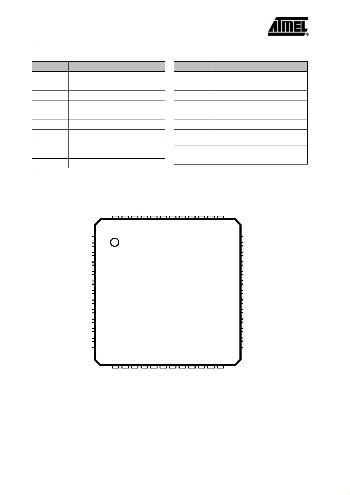
Pinning
TX_DATA
I_CPSW
48 47 46 45 44 43 42 41 40 39 38 37
PU_RX/TX
PU_PULL
PU_VCO
GND_PLL
Name Description
PC Programmable counter
PD Phase detector
RAMP GEN Ramp-signal generator
RC Reference counter
RSSI Received signal-strength indicator
TX DRIVER Buffer amplifier for TX_OUT
TX/RX
SWITCH
Switches VCO signal to IR MIXER
resp. TX DRIVER
VCO Voltage-controlled oscillator
VCO REG Voltage regulator for VCO
RX_ON
TX_ON
VS_MIXER
MIXER_OUT1
MIXER_OUT2
RAMP_SET
CLOCK
DATA
ENABLE
REF_CLK
LD
PU_REG
VS_PLL
VREG
REG_CTRL
VS_REG
GND_CP
VS_CP
1
2
3
4
5
6
7
8
9
10
11
12
13 14 15 16 17 18 19 20 21 22 23 24
CP
VS_VCO
T2801
VTUNE
GND_VCO
VREG_VCO
GND1
DEMOD_TANK1
DEMOD_TANK2
REG_DEC
DAC_DEC
BB_CF
BB_OUT
36
35
34
33
32
31
30
29
28
27
26
25
RAMP_OUT
IF_IN2
IF_IN1
VS_IF
TX_OUT
GND3
RF_IN2
RF_IN1
GND2
IF_TANK2
IF_TANK1
RSSI
2 (27)
Figure 2. Pinning
Rev. A9, 11-Dec-01
Preliminary Information
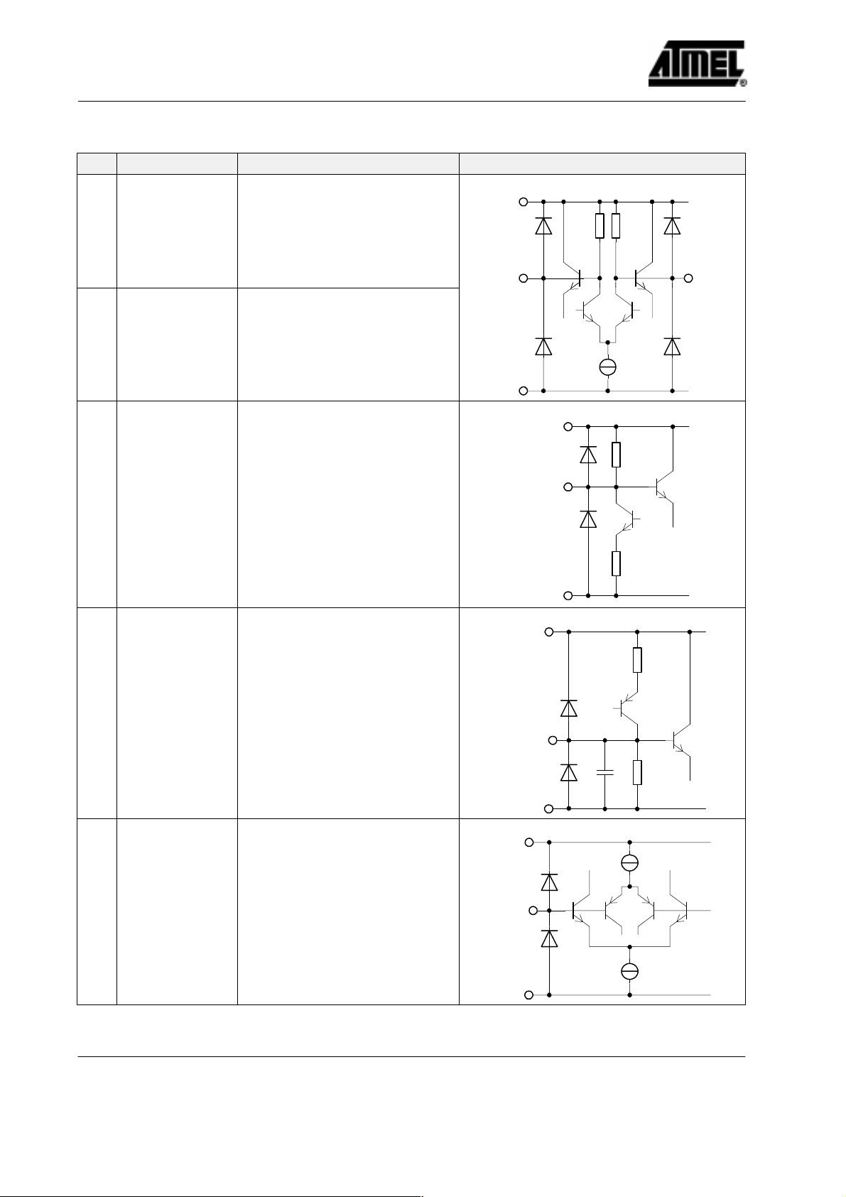
Pin Description
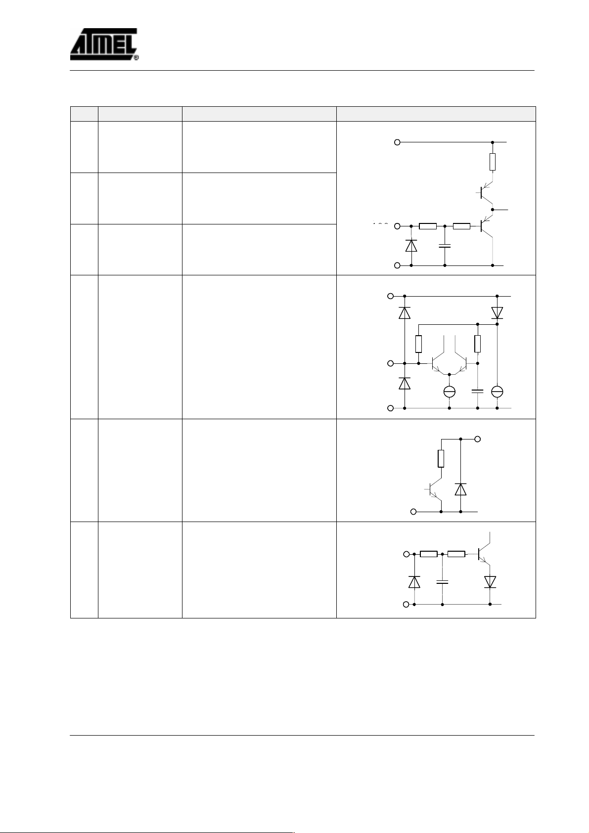
ENABLE
Pin Symbol Function Configuration
1 CLOCK 3-wire-bus: Clock input
2 DATA 3-wire-bus: Data input
3 ENABLE 3-wire-bus: Enable input
VS_PLL
7
CLOCK
DATA
ENABLE
1,2,3
GND_PLL
43
5k 5k
T2801
4 REF_CLK Reference-frequency input
5 LD Lock-detect output
6 PU_REG Power-up input for aux. voltage
regulator
VS_PLL
7
REF_CLK
4
GND_PLL
43
GND_PLL
PU_REG
6
43
10k
100
25k 25k
10k
LD
5
GND_PLL
43
Rev. A9, 11-Dec-01 3 (27)
Preliminary Information
T2801
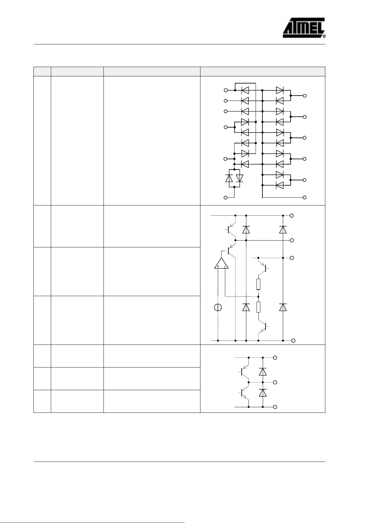
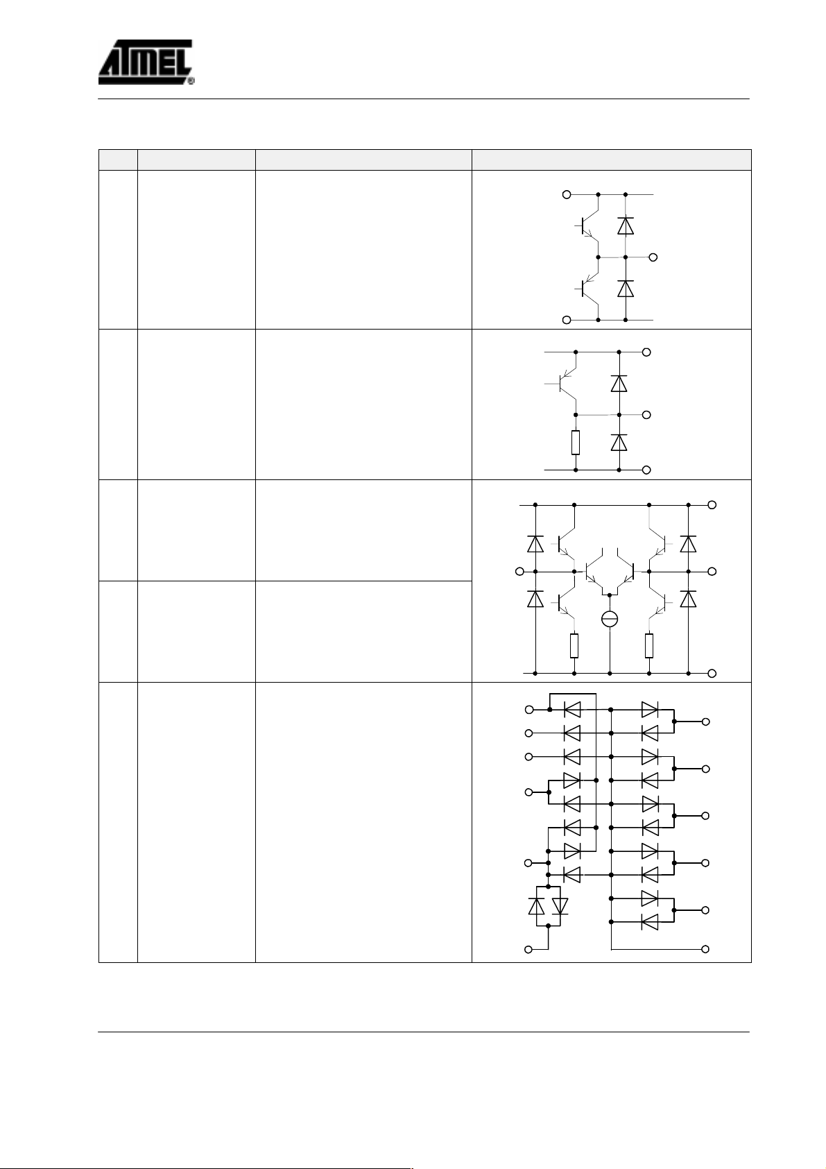
Pin Description (continued)
Pin Symbol Function Configuration
7 VS_PLL PLL supply voltage
VS_PLL
7
VS_REG
10
VS_CP
12
VS_VCO
14
GND1
18
GND2
28
GND3
31
8 VREG Aux. voltage-regulator output
9 REG_CTRL Aux. voltage-regulator control
output
10 VS_REG Aux. voltage-regulator supply
voltage
VS_IF
33
VS_MIXER
42
GND_VCO
16
GND_CP
11
GND_PLL
43
VS_REG
10
REG_CTRL
9
VREG
8
11 GND_CP Charge-pump ground
12 VS_CP Charge-pump supply voltage
13 CP Charge-pump output
4 (27)
Preliminary Information
GND_PLL
43
VS_CP
12
CP
13
GND_CP
11
Rev. A9, 11-Dec-01
Pin Description (continued)
Pin Symbol Function Configuration
14 VS_VCO VCO voltage-regulator supply
voltage
T2801
VS_VCO
14
15 VREG_VCO VCO voltage-regulator control
output
16 GND_VCO VCO ground
17 VTUNE VCO tuning voltage input
18 GND1 Ground
VREG_VCO
15
VTUNE
17
GND_VCO
16
VS_PLL
7
VS_REG
10
VS_CP
12
VS_VCO
14
VREG_VCO
15
GND_VCO
16
GND1
18
GND2
28
GND3
31
VS_IF
33
VS_MIXER
42
GND_VCO
16
GND_CP
11
GND_PLL
43
Rev. A9, 11-Dec-01 5 (27)
Preliminary Information
T2801
Pin Description (continued)
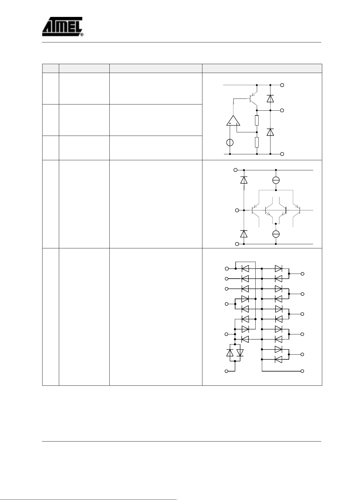
Pin Symbol Function Configuration
19 DEMOD_TANK1 Demodulator tank circuit
VS_MIXER
42
10k 10k
20 DEMOD_TANK2 Demodulator tank circuit
21 DAC_DEC Decoupling PIN for VCO_DAC
22 REG_DEC Decoupling PIN for VCO_REG
DEMOD_
TANK1
19
GND1
18
VREG_VCO
DAC_DEC
GND_VCO
VREG_VCO
DEMOD_
TANK2
20
15
10k
21
400
16
15
2k
23 BB_CF Baseband filter corner-frequency
control input
6 (27)
Preliminary Information
REG_DEC
22
42k
GND_VCO
16
VS_IF
33
BB_CF
23
GND1
18
Rev. A9, 11-Dec-01
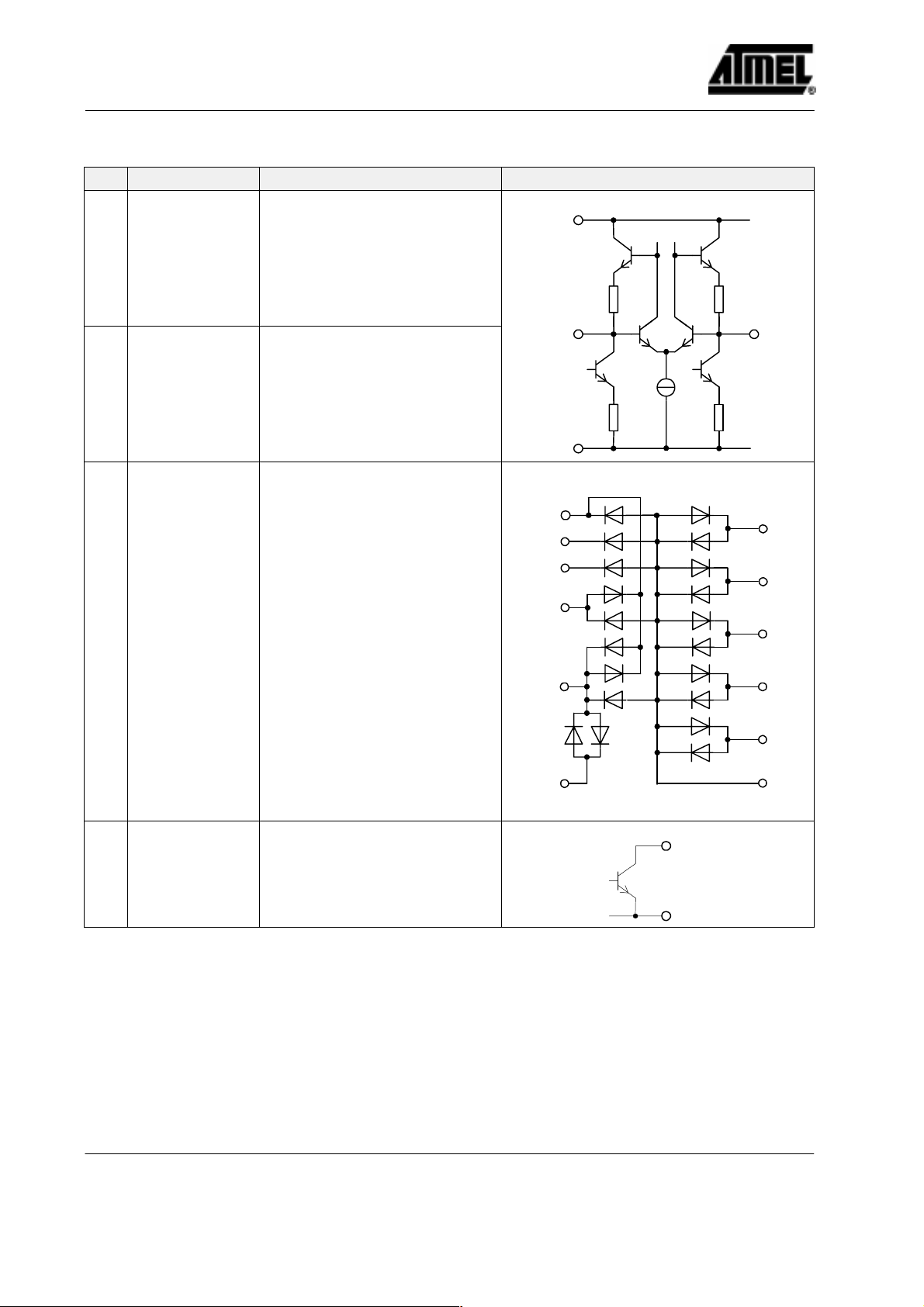
Pin Description (continued)
Pin Symbol Function Configuration
24 BB_OUT Baseband filter output
25 RSSI Received signal-strength indicator
output
26 IF_TANK1 IF tank circuit
VS_IF
33
GND1
18
13k
T2801
BB_OUT
24
VS_IF
33
RSSI
25
GND2
28
VS_IF
33
27 IF_TANK2 IF tank circuit
28 GND2 Ground
IF_TANK1
26
VS_PLL
7
VS_REG
10
VS_CP
12
VS_VCO
14
VS_IF
33
VS_MIXER
42
IF_TANK2
27
GND2
28
GND1
18
GND2
28
GND3
31
GND_VCO
16
GND_CP
11
GND_PLL
43
Rev. A9, 11-Dec-01 7 (27)
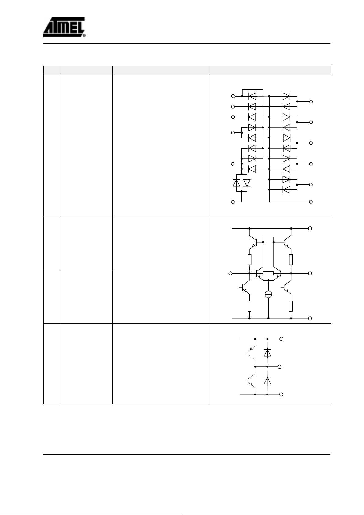
Preliminary Information
T2801
RF_IN1
RF_IN2
Pin Description (continued)
Pin Symbol Function Configuration
29 RF_IN1 RF input of image reject mixer
VS_MIXER
42
30 RF_IN2 RF input of image reject mixer
31 GND3 Ground
RF IN1
29
GND2
28
VS_PLL
7
VS_REG
10
VS_CP
12
VS_VCO
14
VS_IF
33
VS_MIXER
42
RF IN2
30
GND1
18
GND2
28
GND3
31
GND_VCO
16
GND_CP
11
GND_PLL
43
32 TX_OUT TX driver amplifier output for PA
8 (27)
Preliminary Information
TX_OUT
32
GND3
31
Rev. A9, 11-Dec-01
Pin Description (continued)
IF_IN1
IF_IN2
4.3k
Pin Symbol Function Configuration
33 VS_IF IF amplifier supply voltage
T2801
34 IF_IN1 IF input of IF amplifier
35 IF_IN2 IF input of IF amplifier
VS_PLL
7
VS_REG
10
VS_CP
12
VS_VCO
14
VS_IF
33
VS_MIXER
42
IF IN1 IF IN2
34
GND1
GND2
GND3
GND_VCO
GND_CP
GND_PLL
VS_IF
18
28
31
16
11
43
33
35
GND2
28
36 RAMP_OUT Ramp-generator output for PA
power ramping
Rev. A9, 11-Dec-01 9 (27)
VS_MIXER
42
RAMP_OUT
36
GND2
28
Preliminary Information

T2801
Pin Description (continued)
Pin Symbol Function Configuration
37 RAMP_SET Slew-rate setting of ramping signal
56
VS_MIXER
42
RAMP_SET
37
GND2
25
38 RX_ON RX control input
39 TX_ON TX control input
40 MIXER_OUT1 Mixer output to SAW filter
41 MIXER_OUT2 Mixer output to SAW filter
RX_ON
TX_ON
38, 39
GND1
MIXER_
OUT1
40
VS_IF
33
18
5k 5k
270 270
VS_MIXER
42
MIXER_
OUT2
41
GND2
28
10 (27)
Rev. A9, 11-Dec-01
Preliminary Information

Pin Description (continued)
31
Pin Symbol Function Configuration
42 VS_MIXER Mixer supply voltage
VS_PLL
7
VS_REG
10
VS_CP
12
VS_VCO
14
43 GND_PLL PLL ground
VS_IF
33
T2801
GND1
18
GND2
28
GND3
31
GND_VCO
16
GND_CP
11
44 PU_VCO VCO power-up input
45 PU_RX/TX RX/TX power-up input
VS_MIXER
42
VS_VCO
PU_VCO
GND_VCO
GND1
14
44
16
PU_RX/TX
45
18
GND_PLL
43
5k 5k
25k 25k
Rev. A9, 11-Dec-01 11 (27)
Preliminary Information

T2801
Pin Description (continued)
Pin Symbol Function Configuration
46 PU_PLL PLL power-up input
20k
10k 10k
10k
140k
47 TX_DATA TX data input of Gaussian filter and
modulation-compensation circuit
48 I_CPSW Charge pump switch input controls
charge pump current
PU_
PLL
46
GND_
PLL
43
25k 25k
VS_PLL
7
TX_DATA
47
5k 5k
GND_PLL
43
VS_PLL
7
12 (27)
I_CPSW
48
5k
GND_PLL
43
Rev. A9, 11-Dec-01
Preliminary Information

Functional Description
T2801
Receiver
The RF signal at RF_IN is fed to an image rejection mixer
IR_MIXER with its differential outputs MIXER_OUT1
and MIXER_OUT2 driving an IF-SAW filter at
110.592 MHz or 112.32 MHz. The IF amplifiers
IF_AMP1 and IF_AMP2 with an external IF_TANK and
an integrated RSSI function feed the signal to the
demodulator DEMOD working at f = fIF/2 (55 MHz)
and finally to an integrated baseband filter BB. For
demodulator tuning in production an integrated 5-bit digital-to-analog (D/A) converter is provided to control the
on-chip varicap diode.
Transmitter
The transmit data at TX_DATA is filtered by an integrated
Gaussian Filter GF and fed to the fully integrated VCO
operating at twice the output frequency. After modulation
the signal is frequency-divided by 2 and fed via a TX/RX
SWITCH to the TX_DRIVER. This bus-controlled driver
amplifier supplies typical +3 dBm output power at
TX_OUT. A ramp-signal generator RAMP_GEN, provides a ramp signal at RAMP_OUT for the external power
amplifier, is integrated. The slope of the ramp signal is
controlled by a capacitor at the RAMP_SET pin.
Synthesizer
The IR_MIXER, the TX_DRIVER and the
programmable counter PC are driven by the fully
integrated VCO (including on-chip inductors and
varactors). An 3-bit digital-to-analog converter is used to
pretune the frequency. The output signal is frequencydivided to supply the desired frequency to the
TX_DRIVER, 0/90 degree phase shifter for the
IR_MIXER and to be used by the PC for the phase detector PD (fPD = 3.456 MHz). Unlimited multislot operation
is possible by using the integrated advanced closed-loop
modulation concept based on the modulation
compensation circuit MCC.
Power Supply
An integrated bandgap-stabilized voltage regulator for
use with an external low-cost PNP transistor is implemented. Multiple power-down and current saving modes
are provided.
Rev. A9, 11-Dec-01 13 (27)
Preliminary Information

T2801
PLL Principle
Programable counter PC
”– Main counter MC
”– Swallow counter SC
f
= fPD x (SMC x 32 + SSC)
VCO
Phase frequency
detector PD
= 3.456 MHz
f
PD
RF_IN
Charge
pump
ext. loop filter
VCO
DAC
VCO
GF_DATA
f
VCO
Divider
PA driver
by 2
Mixer
Controlled phase shifting
Reference counter RC
REF_CLK
13.824MHz 4
20.736MHz 6
PLL reference
Frequency
REF_CLK
Baseband controller
Modulation Gaussian
compensation MCC filter GF
6.912 MHz
S
RC
310.368MHz
1.152 Mbit/s
TX_DATA
Figure 3.
14 (27)
Rev. A9, 11-Dec-01
Preliminary Information

T2801
The following table shows the LO frequencies for RX and TX for the DECT band plus additional channels for the
extended DECT band. Intermediate frequencies of 110.592 MHz and 112.32 MHz are supported.
Table 1 LO frequencies
Mode fIF/MHz Channel f
TX C9 1881.792 1881.792 34 1
C8 1883.520 1883.520 34 2
... ... ... ... ...
C1 1895.616 1895.616 34 9
C0 1897.344 1897.344 34 10
C10 1899.072 1899.072 34 11
C11 1900.800 1900.800 34 12
... ... ... ... ...
C29 1931.904 1931.904 34 30
C30 1933.632 1933.632 34 31
RX 110.592 C9 1881.792 1771.200 32 1
C8 1883.520 1772.928 32 2
... ... ... ... ...
C1 1895.616 1785.024 32 9
C0 1897.344 1786.752 32 10
C10 1899.072 1788.480 32 11
C11 1900.800 1790.208 32 12
... ... ... ... ...
C29 1931.904 1821.312 32 30
C30 1933.632 1823.040 32 31
RX 112.320 C9 1881.792 1769.472 32 0
C8 1883.520 1771.200 32 1
... ... ... ... ...
C1 1895.616 1783.296 32 8
C0 1897.344 1785.024 32 9
C10 1899.072 1786.752 32 10
C11 1900.800 1788.480 32 11
... ... ... ... ...
C29 1931.904 1819.584 32 29
C30 1933.632 1821.312 32 30
/MHz f
ANT
/MHz S
VCO
MC
S
SC
Formula
TX: f
RX: f
= f
ANT
= 1.728 MHz × (32 × SMC + SSC) + f
ANT
= 1.728 MHz × (32 × SMC + SSC)
VCO
IF
Rev. A9, 11-Dec-01 15 (27)
Preliminary Information

T2801
Control Signals
T able 2
Signal Function
I_CPSW Controls the charge pump current
PU_REG Activates AUX voltage regulator supplying the complete transceiver.
PU_VCO Activates VCO voltage regulator which supplies only the VCO.
PU_RX/TX Activates RX/TX switch.
PU_PLL Activates PLL circuits: PC, PD, CP, RC
RX_ON Activates RX circuits: BBF, DEMOD, IF AMP, IR MIXER
TX_ON Activates TX circuits: TX-DRIVER, RAMP GEN. Starts RAMP SIGNAL at RAMP OUT.
Data Word 1
Bit D10
Data Word 1
Bit D9
T able 3
PU_REG 1 1 1
PU_VCO 1 1 1
PU_RX/TX 1 1 1
PU_PLL 1 1 1
RX_ON 0 1 1
TX_ON 1 0 1
BB filter OFF ON OFF
Demodulator OFF ON OFF
IF amplifiers and RSSI OFF ON ON
IR mixer OFF ON ON
RX switch OFF ON ON
TX switch ON OFF OFF
TX driver ON OFF OFF
Ramp generator ON OFF OFF
Programmable counter ON ON ON
Voltage-controlled oscillator ON ON ON
Gaussian filter ON OFF OFF
Phase detector / charge pump ON ON ON
Modulation compensation circuit ON OFF OFF
Reference counter ON ON ON
Typ. current consumption / mA @ VS = 3.2 V 54 85 80
Activates GF in TX mode.
Activates MCC in TX mode.
Mode TX Mode RX Mode RSSI Only
16 (27)
Rev. A9, 11-Dec-01
Preliminary Information

T2801
Serial Programming Bus
The transceiver is programmed by the 3-wire bus
(CLOCK, DATA and ENABLE).
After setting enable signal to low condition, on the rising
edge of the clock signal, the data is transferred bit by bit
into the shift register, starting with the MSB-bit. After
enable returning to high condition the programmed
information is loaded into the addressed latches,
according to the addressbit condition (last bit). Additional
leading bits are ignored and there is no check made how
Data Word 1
MSB LSB
Data bits Address
D22 D21 D20 D19 D18 D17 D16 D15 D14 D13 D12 D11 D10 D9 D8 D7 D6 D5 D4 D3 D2 D1 D0 A0
RC SC MC VCOS 1 1 GF MCC GFCS VCODAC CPCS 1
Data Word 2
many pulses arrived during enable-low condition. During
enable low condition the bus current is increased to speed
up the bus logic.
The programming of the transceiver is separated into two
data words. Data word 1 controls mainly the channel information together with settings, which are closely
related with the channel. Dataword 2 holds setup information, which is adjusted during production.
bit
Data Word 1 Programs
PLL Settings
With the Reference Counter bits D21 – D22
RC (Reference Counter)
D22 D21 S
0 0 3 10.368 MHz
0 1 4 13.824 MHz
1 0 6 20.736 MHz
With the Main Counter bits D14 – D15
MC (Main Counter)
D15 D14 S
0 0 32
0 1 33
1 0 34
1 1 35
RC
REF_CLK
MC
E10 E9 E8 E7 E6 E5 E4 E3 E2 E1 E0 A0
DEMODDAC MCCS TEST 0
SC (Swallow Counter)
D20 D19 D18 D17 D16 S
0 0 0 0 0 0
0 0 0 0 1 1
0 0 0 1 0 2
... ...
1 1 1 0 1 29
1 1 1 1 0 30
1 1 1 1 1 31
SC
With the Swallow Counter bits D16 – D20
Rev. A9, 11-Dec-01 17 (27)
Preliminary Information

T2801
VCO Select (RX/TX VCO)
With bit D13
Used to switch between RX/TX VCO
D13 VCOS (VCO Select)
0 RX-VCO
1 TX-VCO
Gaussian Filter on/off
With bit D10
GF is used only in TX mode
D10 GF (Gaussian Filter)
0 OFF
1 ON
Modulation Compensation Circuit on/off
With bit D9
MCC is used only in TX mode
D9 MCC (Modulation Compensation Circuit)
0 OFF
1 ON
GFCS Adjustment
With bit D6 – D8
Only in TX mode ef fective for setting the frequency devi-
ation of the modulation
GFCS (Gaussian Filter Settings)
D8 D7 D6 GFCS
0 0 0 60%
0 0 1 70%
0 1 0 80%
0 1 1 90%
1 0 0 100%
1 0 1 110%
1 1 0 120%
1 1 1 130%
VCO_DAC Adjustment
With bit D3 – D5
Used to pretune the VCO frequency in case of production
tolerances of the device. Tuning voltage in locked condition should be around 1.8 V at room temperature. This
gives margin for ambient temperature changes.
Pretune DAC Voltage
D5 D4 D3 f
0 0 0 –5
0 0 1 ...
0 1 0 ...
0 1 1 ...
1 0 0 ...
1 0 1 ...
1 1 0 ...
1 1 1 5
VCO
/%
CPCS Adjustment
With bit D0 – D2
Used to adjust the charge pump current. This can be used
to compensate the change of the tuning sensitivity over
frequency and device tolerances.
CPCS (Charge-Pump Current Settings)
D2 D1 D0 CPCS
0 0 0 –4
0 0 1 –3
0 1 0 –2
0 1 1 –1
1 0 0 0
1 0 1 1
1 1 0 2
1 1 1 3
18 (27)
Rev. A9, 11-Dec-01
Preliminary Information

Data Word 2 Programs
T2801
DEMODDAC Adjustment
With bits E6 – E10
Only in RX mode ef fective. Used to tune the demodulator
center frequency and allows to compensate tolerances of
external components and the T2801.
Demod DAC Voltage
E10 E9 E8 E7 E6 f
0 0 0 0 0 –5
0 0 0 0 1 ...
0 0 0 1 0 ...
1 1 1 0 1 ...
1 1 1 1 0 ...
1 1 1 1 1 5
IFcenter
...
%
MCCS Adjustment
With bits E3 – E5
Only in TX mode effective. Adjusts the modulation com-
pensation circuit for closed loop modulation. This
adjustment is done with a test sequence of a long stream
of ,1‘ – ,0‘. The correct setting is achieved, if the modulation is not affected by the PLL.
TEST Mode Settings
With bit E0 – E2 and D11
In normal operation Lock detect output is used. All other
settings are for test only.
D11 E2 E1 E0 Signal at lock
detect output
1 0 0 0 Lock detect Active
0 0 0 1 RC out Active
1 0 1 0 PC out Active
X 0 1 1 MCCTEST:
RC out divided by
2048
1 1 0 0 Lock detect High imp.
0 1 0 1 RC out High imp.
1 1 1 0 PC out High imp.
X 1 1 1 GFTEST: RC out
divided by 2
CP mode
Active
High imp.
MCCS (Modulation Compensation Settings)
E5 E4 E3 MCCS
0 0 0 60%
0 0 1 70%
0 1 0 80%
0 1 1 90%
1 0 0 100%
1 0 1 110%
1 1 0 120%
1 1 1 130%
Rev. A9, 11-Dec-01 19 (27)
Preliminary Information

T2801
3-Wire Bus Protocol Timing Diagram
DATA
CLOCK
ENABLE
TL
TPER
Figure 4.
Description Symbol Min. Value Unit
Clock period TPER 125 ns
Set time data to clock TS 60 ns
Hold time data to clock TH 60 ns
Clock pulse width TC 60 ns
Set time enable to clock TL 200 ns
Hold time enable to data TEC 0 ns
Time between two protocols TT 250 ns
TS
TC
TH
TEC
TT
16525
TX DATA Timing
RefCLK
TX_DATA
T
T
Set-up time TX DATA TS 10 ns
Hold time TX DATA TH 10 ns
Figure 5. TX DATA timing
H
S
TS and TH must be considered for both (falling and
rising) edges of RefCLK when using REF_CLK =
10.368 MHz.
Absolute Maximum Ratings
All voltages refer to GND
Parameter Symbol Min. Max. Unit
Supply voltage regulator Pin 10 V
Supply voltage Pins 7, 12, 14, 33 and 42 V
Logic input voltage Pins 1, 2, 3, 38, 39, 44,
45, 46, 47 and 48
Junction temperature T
Storage temperature T
S_REG
S
V
IN
jmax
stg
3.2 4.7 V
3.0 4.7 V
– 0.3 V
S
150 C
–40 150 C
V
Thermal Resistance
Parameter Symbol Value Unit
Junction ambient R
20 (27)
Preliminary Information
thJA
t.b.d. K/W
Rev. A9, 11-Dec-01

T2801
Operating Range
Parameter Symbol Min. Typ. Max. Unit
Supply voltage regulator Pins 10 V
Supply voltage Pins 7, 12, 14, 33 and 42 V
Ambient temperature T
S_REG
S
amb
Electrical Characteristics
Test conditions (unless otherwise specified): V
Parameter Test Conditions / Pins Symbol Min. Typ. Max. Unit
IR mixer Pins 29, 30, 40 and 41
Input impedance Pins 29 and 30 Z
Input matching Pins 29 and 30 VSWR
Image rejection ratio Pins 40 and 41 IRR 20 dB
DSB noise figure Pins 40 and 41 NFDSB=
Conversion gain R
= 200 Ω G
load
Input interception point Pins 40 and 41 IIP3 –10 dBm
IF amplifier Pins 26, 27, 34 and 35
Input impedance Pins 34 and 35 Z
Lower cut-off frequency fl
Upper cut-off frequency fu
Power gain Gp 85 dB
Bandwidth of external tank
circuit
Noise figure NF 9 dB
RSSI Pins 25, 34 and 35
RSSI sensitivity at IF_IN1, IF_IN2
RSSI compression at IF_IN1, IF_IN2
RSSI dynamic range DR 80 dB
RSSI resolution Slope of the RSSI has to be
steady
RSSI rise time Pin = 30 to 100 dBµV, Pin 25 t
RSSI fall time Pin = 100 to 30 dBµV, Pin 25 t
Quiescent output current @ Pin < 20 dBµV at IF_IN1,
IF_IN2 Pin 25
Maximum output current @ Pin = 100 dBµV at
IF_IN1, IF_IN2 Pin 25
S_REG
= 3.2 V, T
amb
= 25°C
NFSSB
Pins 26 and 27 BW3dB 10 MHz
P
Pins 34 and 35
P
Pins 34 and 35
Acc ±2 dB
I
I
3.2 3.6 4.6 V
3.0 3.0 4.6 V
–25 +85 C
in
in
50 Ω
<2:1
10 dB
conv
in
3dB
3dB
min
max
r
f
out
out
200 400 Ω
11 dB
90 MHz
130 MHz
20 dBµV
100 dBµV
1 µs
1 µs
30 µA
150 µA
Rev. A9, 11-Dec-01 21 (27)
Preliminary Information

T2801
Electrical Characteristics (continued)
Test conditions (unless otherwise specified): V
FM demodulator, BB-Filter Pins 19, 20, 23 and 24
Co-channel rejection ratio @ Pin = –75 dBm at
IR-mixer input
Sensitivity Quality factor of external
tank circuit approx. 20,
f
= FIF/2, Pin 24
res
Amplitude of recovered
signal
Nominal deviation of signal
± 288 kHz, Pin 24
Corner frequency Pin 23: C = 68 pF f
Output voltage DC range Pin 24 V
DAC for FM demodulator (internally connected)
DEMOD_DAC range (see bus protocol E6 ... E10) f
VCO
RX–VCO frequency range VCOS = ‘0’ Bit D13 f
TX–VCO frequency range VCOS = ‘1’ Bit D13 f
Tuning gain G
Frequency control voltage
range
VCO_DAC range (see bus protocol D3 ... D5) ∆f
PLL
Scaling factor prescaler S
Scaling factor main counter S
Scaling factor swallow
counter
External reference input
AC coupled sinewave
frequency
External reference input
AC coupled sinewave
voltage
Scaling factor reference
counter
Charge pump Pin 13
Output current VCP = V
VS_CP
I_CPSW = ‘1’ Pin 48
Output current VCP = V
VS_CP
I_CPSW = ‘0’ Pin 48
Current scaling ICP =
I
CP_nom
+ CPCS * I
(see bus protocol D0 ... D2)
Leakage current I
S_REG
= 3.2 V, T
amb
= 25°C
Pin 17 V
f
REF_CLK
Pin 4
V
Pin 4
/ 2,
/ 2,
I
I
I
CP_step
UnitMax.Typ.Min.SymbolTest Conditions / PinsParameter
CCRR 10 dB
S 0.5 V/MHz
A 450 mVss
c
outDC
IFcenter
vco
vco
tune
tune
vco,DAC
PSC
MC
S
SC
REF_CLK
S
RC
CP_nom
CP_nom
CP_step
L
1750 1840 MHz
1860 1950 MHz
0.4 2.8 V
50 250
680 kHz
1 Vs–1 V
± 5 %
40 MHz/V
± 5 %
32 / 33
32 / 33 / 34 / 35
0 31
10.368
13.824
20.736
MHz
MHz
MHz
mV
3 / 4 / 6 / 8
± 6.5 mA
± 1.2 mA
0.2 mA
± 100 pA
RMS
22 (27)
Rev. A9, 11-Dec-01
Preliminary Information

T2801
Electrical Characteristics (continued)
Test conditions (unless otherwise specified): V
Gaussian transmit filter (Gaussian shape B∗T = 0.5)
Tx data filter clock 12 taps in filter f
Frequency deviation GF
Frequency deviation scaling GFFM = GF
FM_nom
(see bus protocol D6 ... D8)
Modulation compensation circuit
Oversampling OVS 6
Digital sum variation DSV 85
Current scaling factor (see bus protocol E3 ... E5) MCCS 60 130 %
VCO switch and TX driver Pin 32
Power gain @ Pin = –40 dBm Gp 30 dB
Output impedance Pin 32 Z
Maximum output power Pin 32 P
Gain compression @ TX_RF_OUT, Pin 32 P
Output interception point Pin 32 OIP3 10 dBm
Ramp generator Pins 36 and 37
Minimum output voltage According to RAMP_SET
input
Maximum output voltage According to RAMP_SET
input
Rise time C
Fall time C
= 270 pF at Pin 37 t
ramp
= 270 pF at Pin 37 t
ramp
Lock detect and test mode output Pin 5
Lock detect output,
test mode output
locked = ‘1’, unlocked = ‘0’
test modes (see bus protocol
E0 ... E2)
Leakage current V
Saturation voltage I
= 4.6 V I
OH
= 0.5 mA V
OL
Auxiliary regulator Pins 8, 9 and 10
Output voltage V
Supply voltage rejection V
= 3 V Pin 8 V
SREG
= VDC + 0.1 V
Pin10
f
= 0.1 to 10 kHz
Pin10
C
= 100 nF
Pin8
VCO regulator Pins 14, 15 and 12
Output voltage V
= 3 V Pin 15 V
SVCO
3-wire bus
Clock f
S_REG
= 3.2 V, T
* GFCS
pp
= 25°C
amb
TXFCLK
FM_nom
13.824 MHz
±350 kHz
GFCS 60 130 %
out
max
1dB
V
min
V
max
r
f
100 Ω
0 3 dBm
1 dBm
0.2 V
1.95 V
5 µs
5 µs
LD
L
SL
REG
2.9 3.0 3.1 V
0.4 V
SVR t.b.d. dB
REG_VCO
Clock
2.6 2.7 2.8 V
6.912 MHz
UnitMax.Typ.Min.SymbolTest Conditions / PinsParameter
5 µA
Rev. A9, 11-Dec-01 23 (27)
Preliminary Information

T2801
pp y
Electrical Characteristics (continued)
Test conditions (unless otherwise specified): V
Logic input levels (CLOCK, DATA, ENABLE, RX_ON, TX_ON, PU_VCO, TX_DATA, I_CPSW)
Pins 1, 2, 3, 38, 39, 44, 47 and 48
High input level = ‘1’ V
Low input level = ‘0’ V
High input current = ‘1’ I
Low input current = ‘0’ I
Standby control Pins 6, 45 and 46
Power up
PU_REG = ‘1‘
PU_RX/TX = ‘1‘
PU_PLL = ‘1‘
High input level
Standby
PU_REG = ‘0‘
PU_RX/TX = ‘0‘
PU_PLL = ‘0‘
Low input level
Power up
PU_REG = ‘1‘
PU_RX/TX = ‘1‘
VPU = 3 V Pin 6
VPU = 5.5 V Pin 45
= 3.2 V, T
S_REG
Pin 6
Pin 45
Pin 46
Pin 6
Pin 45
Pin 46
= 25°C
amb
iH
iL
iH
iL
V
PU_REG
V
PU_RX/TX
V
PU_PLL
V
PU_REG,OFF
V
PU_RX/TX,OFF
V
PU_PLL,OFF
I
PU_REG
I
PU_RX/TX
1.5 V
–5 5 µA
–5 5 µA
2.0 V
20
60
30
80
0.5 V
0.7 V
40
100
UnitMax.Typ.Min.SymbolTest Conditions / PinsParameter
µA
µA
PU_PLL = ‘1‘
High input current
VPU = 3 V Pin 46
VPU = 5.5 V
I
PU_PLL
Standby
PU_xxxx = ‘0’
Low input current
Settling time
VS = 0 → active operation
Settling time
standby → active operation
Settling time
active operation → standby
VPU = 0 V Pin 6,
I
PU,OFF
VPU = 0.5 V Pins 45, 46
Switched from
VS = 0 to VS = 3V t
Switched from
PU = ‘0’ to PU = ‘1’ t
Switched from
PU = ‘1’ to standby t
Power supply Pins 7, 10, 12, 14, 33 and 42
Total supply current
RX I
RSSI only I
TX I
TX (MCC, GF active) I
Standby current PU_RX/TX = GND I
Supply current CP V
= 3 V, PLL in lock
VS_CP
condition Pin 13
I
soa
ssa
sas
CP
100
200
125
300
150
400
0.1
1
µA
µA
µA
µA
< 10 µs
< 10 µs
< 2 µs
S
S
S
S
S
85 mA
82 mA
54 mA
58 mA
1 10 µA
1 µA
24 (27)
Rev. A9, 11-Dec-01
Preliminary Information

Application Circuit
33 pF
180 nH
SAW
Filter
TFS
112B
33 pF
15 pF
270 nH
RAMP_OUT
TX_OUT RF_IN
68 pF
T2801
100 nH
18 pF
RSSI
RX_ON
TX_ON
PU_VCO
PU_RX/TX
PU_PLL
TX_DATA
I_CPSW
CLOCK
DATA
ENABLE
REF_CLK
LD
PU_REG
15 pF
560 pF
37 RAMP_SET
RAMP_OUT 36
38 RX_ON
39 TX_ON
40 MIXER_OUT1
41 MIXER_OUT2
42 VS_MIXER
43 GND_PLL
44 PU_VCO
45 PU_RX/TX
46 PU_PLL
47 TX_DATA
48 I_CPSW
1 CLOCK
VS_IF 33
IF_IN1 34
IF_IN2 35
T2801
4 REF_CLOCK
3 ENABLE
2 DATA
GND3 31
TX_OUT 32
6 PU_REG
5 LD
GND2 28
RF_IN1 29
RF_IN2 30
7 VS_PLL
IF_TANK2 27
DEMOD_TANK2 20
DEMOD_TANK1 19
VREG_VCO 15
10 VS_REG
9 REG_CTRL
8 VREG
4.7 nF
RSSI 25
IF_TANK1 26
BB_OUT 24
BB_CF 23
REG_DEC 22
DAC_DEC 21
GND1 18
VTUNE 17
GND_VCO 16
VS_VCO 14
CP 13
12 VS_CP
11 GND_CP
220 pF
68 pF
2.2 nF
100 pF
tbd
22 nF
180Ω150 nF
56 pF 470 nF
BB_OUT
tbd
BC808
or similar
tantal tantal
VCC
Figure 6. Application circuit
Rev. A9, 11-Dec-01 25 (27)
Preliminary Information

T2801
Package Information
26 (27)
Rev. A9, 11-Dec-01
Preliminary Information

T2801
Ozone Depleting Substances Policy Statement
It is the policy of Atmel Germany GmbH to
1. Meet all present and future national and international statutory requirements.
2. Regularly and continuously improve the performance of our products, processes, distribution and operating systems
with respect to their impact on the health and safety of our employees and the public, as well as their impact on
the environment.
It is particular concern to control or eliminate releases of those substances into the atmosphere which are known as
ozone depleting substances (ODSs).
The Montreal Protocol (1987) and its London Amendments (1990) intend to severely restrict the use of ODSs and forbid
their use within the next ten years. Various national and international initiatives are pressing for an earlier ban on these
substances.
Atmel Germany GmbH has been able to use its policy of continuous improvements to eliminate the use of ODSs listed
in the following documents.
1. Annex A, B and list of transitional substances of the Montreal Protocol and the London Amendments respectively
2. Class I and II ozone depleting substances in the Clean Air Act Amendments of 1990 by the Environmental
Protection Agency (EPA) in the USA
3. Council Decision 88/540/EEC and 91/690/EEC Annex A, B and C (transitional substances) respectively.
Atmel Germany GmbH can certify that our semiconductors are not manufactured with ozone depleting substances
and do not contain such substances.
8.
We reserve the right to make changes to improve technical design and may do so without further notice.
Parameters can vary in different applications. All operating parameters must be validated for each customer
application by the customer. Should the buyer use Atmel products for any unintended or unauthorized application,
the buyer shall indemnify Atmel against all claims, costs, damages, and expenses, arising out of, directly or
indirectly, any claim of personal damage, injury or death associated with such unintended or unauthorized use.
Data sheets can also be retrieved from the Internet: http://www.atmel–wm.com
Atmel Germany GmbH, P.O.B. 3535, D-74025 Heilbronn, Germany
Telephone: 49 (0)7131 67 2594, Fax number: 49 (0)7131 67 2423
Rev. A9, 11-Dec-01 27 (27)
Preliminary Information
 Loading...