


Table of Contents
Section 1
Introduction...........................................................................................1-1
1.1 Device Support .................................. ....... ...... ....... ...... ....... ......................1-1
Section 2
Getting Started......................................................................................2-1
2.1 Unpacking the System..............................................................................2-1
2.2 System Requirements...............................................................................2-1
Section 3
Connecting the System.........................................................................3-1
Section 4
Hardware Description...........................................................................4-1
4.1 Jumpers, Links and their Functions ..........................................................4-2
4.2 External Connections................................................................................4-2
Section 5
Installing the Software ..........................................................................5-1
5.1 Windows 95 ..............................................................................................5-1
5.2 Windows 3.1 .............................................................................................5-1
Section 6
How to Use the Software......................................................................6-1
6.1 Projects.....................................................................................................6-1
6.2 Files ..........................................................................................................6-1
Section 7
Programming Using the Board ...................... .... ..... ..... .........................7-1
7.1 Device Orientation ............................. .............................................. ...... ...7-1
7.2 Voltage Selection......................................................................................7-1
7.3 Power and Lead Connections...................................................................7-2
Section 8
Brown-Out Detector..............................................................................8-1
Section 9
Board Applications................................................................................9-1
9.1 Using Switches and LEDs.........................................................................9-1
9.2 Using External Connections......................................................................9-1
i

Table of Contents
9.2.1 Misc. Header ......................................................................................9-2
9.3 Using Analog Functions ............................................................................9-2
9.3.1 Analog Port: Marked on Board ...........................................................9-2
9.3.2 Using Internal Reference....................................................................9-2
9.3.3 Using External Reference...................................................................9-3
9.4 Using External RAM..................................................................................9-3
9.4.1 RAM Recommendations.....................................................................9-3
9.4.2 RAM Socket Pin Layout......................................................................9-3
9.4.3 Address Latch................. ....... ...... .............................................. ...... ...9-3
9.5 Using LCD Connections............................................................................9-3
9.6 Using RS232.............................................................................................9-4
9.7 Programming In-System ...........................................................................9-4
9.8 ISP Header Layout....................................................................................9-5
9.9 Interface Using Resistors..........................................................................9-5
9.10 Using an Analogue Multiplexer IC.............................................................9-5
9.10.1 Using Real Time Clock.......................................................................9-6
ii

Section 1
Introduction
Welcome to the megaAVR™ Starter Kit.
This system incorporates an applications board and in-system programming hardware
key for programming AVR
README.TXT file included with the software for installation information.
®
devices in your application. Be sure to check the
1.1 Device Support
The system software currently has support for the following devices.
■
ATmega603
■
ATmega603L
■
ATmega103
■
ATmega103L
Software upgrades for new devices will be available in the AVR section of the Atmel
website, which is located at http://www.atmel.com.
megaAVR™ Starter Kit Manual 1-1

Introduction
1-2 megaAVR™ Starter Kit Manual

Section 2
Getting Started
2.1 Unpacking the System
2.2 System Requirements
Contents of box:
■
Evaluation Board
■
Disk set consisting of AVR ISP software and STK300 Application Builder
■
In-System Programming (ISP) Dongle
■
ISP Ribbon Cable
The minimum hardware and software requirements are:
■
80386 Processor or Above
■
1MB Ram
■
1MB Free Hard Disk Space
■
Windows 3.1 or Windows 95
megaAVR™ Starter Kit Manual 2-1

Getting Started
2-2 megaAVR™ Starter Kit Manual
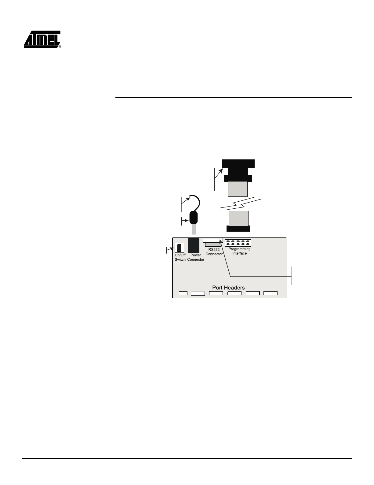
Section 3
PLUG HEADER ON LEAD
INTO PROGRAMMING
INTERFACE - KEY WAY
GIVES ORIENTATION
CONNECT LEAD
SUPPLIED TO DONGLE
AND INSERT IN
PC PRINTER PORT
POWER SUPPLY
9 - 15V DC
7 - 12V AC
ON-OFF SWITCH
RS 232 CONNECTOR
NOT USED FOR
PROGRAMMING
POWER CONNECTOR
5.5/2.1 BARREL
Connecting the System
megaAVR™ Starter Kit Manual 3-1
A Power Supply is required with a standard 2.1mm barrel connector . It can be AC 7 12V or DC 9 - 15V . The conne ctor is inse rted into the power con nection socket as
shown, above.
The programming lead supplied is fitted into the Dongle case and the other end is
inserted into the programming interface on the board as shown.
The Dongle case i s co nnect ed to one o f the prin ter ports o n the PC. I f this is not LPT1,
then you will need to change t he printer port se tting in the so ftware—see s oftware section for details.

Connecting the System
3-2 megaAVR™ Starter Kit Manual
Hardware Description
LCD CONNECTOR
ANALOG REFERENCE
VOLTAGE ADJUSTMENT
PLUG IN MEGA
BOARD HERE
ANALOG I/P
PORT A DIGITAL
4 MHz CRYSTAL
PORT B HEADER
PORT C HEADER
PORT D JUMPERS
DISABLE SWITCHES
PORT D HEADER
MISC. HEADER
FOR NON-PORT PINS
JP2 - JUMPER
FOR BROWN-OUT
AT 2.9V OR 4.5V
8 LEDS ON
PORT B
8 SWITCHES
ON PORT D
JP1 JUMPER FOR
3.3 OR 5V VCC SELECT
ON-OFF
SWITCH
POWER INPUT
9-15V DC
OR 7-12 AC
RS232
PORT B JUMPERS
DISABLE LEDS
POWER ON AND
PROG LIGHTS
SELECTOR
FOR RS232
ISP INTERFACE
ADDRESS LATCH
IC FOR RAM
EXTERNAL
SRAM SOCKET
EXTERNAL
MEMORY EXPANSION
LCD CONTRAST
ADJUSTMENT
LK1 - CUT FOR A/D
EXTERNAL REFERENCE
O/P PINS FOR -VE
SUPPL Y T O
OPAMP ETC.
PORT E HEADER
The main features of the board are shown in the diagram below.
Section 4
megaAVR™ Starter Kit Manual 4-1
Note:
There are a number of jumpers on the board which are used to select different
operations and voltages. The default jumper settings are for programming operations at 5V JP1 Closed, with brown-out also set to 5V JP2 Open.
To carry out other operations, some jumpers may have to be removed—refer to
the relevant section for details. A full list of the jumpers and links are given in the
following table.
Hardware Description
4.1 Jumpers, Links and their Functions
Jumper Function Open Closed Default
JP1 V oltage select 5V 3.3V Open
JP2 Brown-out select 2.9V 4.5V Closed
PE0 RS232 RXD Port E.0 RXD Port E.0
PE1 RS232 TXD Port E.1 TXD Port E.1
Port B LEDs LEDs Disabled LEDs Enabled Closed
Port D Switches Switches Disabled Switches Enabled Closed
4.2 External Connections
LK1 Analog
Reference
CUT Under
Board
LCD Contrast If Cut, add
If LK1 cut, then
EXTERNAL REF
from header
extra resistor
ONBOARD POT Closed
Contrast Pot Closed
All Ports are brought out to edge of board on to headers. Each header has a VCC and
Ground pin for power supply to external circuits. Port F is the Analog input port and is on
the header marked “Analog”. There is an ex tra six-pin header for miscellaneous fun ctions—Read, Write, ALE, Reset, Ground and VCC.
See sections “Using External Connections” on page 9-1 and “Using Analog Functions”
on page 9-2 for details.
4-2 megaAVR™ Starter Kit Manual

Section 5
Installing the Software
5.1 Windows 95
5.2 Windows 3.1
To install the software, insert the supplied dis k or CD-RO M i nto yo ur co mpu ter and per form the following steps:
1. Click on the “Start” button.
2. Select “Settings”.
3. Select “Control Panel”.
4. Choose “Add/Remove Programs”.
5. Click the “Install” button.
6. Follow On-Screen prompts.
The software will then be installed onto your computer and an Icon will be added to your
start menu.
Choose “RUN” from Program Manager, and enter A:\SETUP.EXE as the filename.
Press the “OK” button and the software installation program will begin.
The software will the n b e i ns tal led on to you r c omp uter a nd an Ico n a nd Pr og ra m Gr ou p
will be added to Program Manager.
Note:
In the unlikely event that you have any problems installing the software or suspect that
you have faulty media, please contact the Atmel Starter Kit hotline:
Telephone Number:
Fax Number:
Email:
On some PCs, especially laptops, programming problems may occur if the
BIOS Parallel Port settings are set to EPP Version 1.7. If programming problems do happen, ensure that the Parallel Port settings in your BIOS are set to
EPP V1.9 not V1.7. This applies to both Windows 95 and Windows 3.1 based
PCs.
(44) 1970 621 049
(44) 1970 621 040
stk300_support@atmel.com
megaAVR™ Starter Kit Manual 5-1

Installing the Software
5-2 megaAVR™ Starter Kit Manual

Section 6
How to Use the Software
The software is fully context sensitive. This means that pressing F1 at any time will bring
up help information about the current option that you have selected.
Please note that the toolbar icons referred to in the text have ToolTip’s, so if you want to
know the function of any particular butto n, hold your mouse p ointer over the button i n
question and its function will be displayed.
■
Starting a Project
■
In-System Programming (ISP)
■
Hardware Requirements
■
Projects
■
Data Files
■
Editing Data
6.1 Project s
6.2 Files
If you have used a high-end professional development system, you will be familiar with
the project concept. Essentially, this is a collection of details and data which are managed by the program on your behalf. In the AVR, you have both Program Memory and
non volatile Data Memory (EEPROM), with various security and device options. The
project manager keep s thi s information together for y ou so y ou don't hav e to remember
and reload all the various files every time you use the programmer.
The project manager will all ow you to store inform ation like the project nam e and the
project identifier. It also has a small notepad for you to store comments about the
project.
Before you can start a programming session, you must either open an existing project or
start a new project. You can op en a pr oject, or create a new on e, by e ither goi ng to th e
Project menu and selecting “New” or “Open”, or by using the “New Project” or “Open
Project” buttons on the toolbar.
Once a project is open, you can load the files that you need to program into the device.
Files may be loaded by either using the “Load” command in the File menu or by using
the “Open” icon on the toolbar.
The program will automatically decode your files whether they are in Intel Hex format,
Atmel Generic , Binar y o r Motor ola S rec ord . The file y ou c hoose wil l be loaded into the
window, then it is displayed on the top of the desktop. Therefore, if y ou have the
EEPROM Data Memory window on top, it will load the data into that window.
megaAVR™ Starter Kit Manual 6-1

How to Use the Software
6-2 megaAVR™ Starter Kit Manual
Section 7
Programming Using the Board
7.1 Device Orientation
7.2 Voltage Selection
Before programming a devi ce using the prog ramming modul e, the device adap ter must
be inserted c orrec tly int o the pr ogramm ing un it. The a dapter itsel f has a c orner cut-off ,
which locates pin 1 of the device and matches the marking on the main uni t. This
adapter should be prefitted, bu t can be replaced if th e device programming life is
exceeded—refer to your supplier to obtain a new device adapter.
The orientation of the devi ce is vitall y i mportan t. If yo u put it in the wr ong way then you
may damage the device. DO NOT PLUG A DEVICE ADAPTER IN WITH THE POWER
SWITCHED ON or you ma y d ama ge i t. S imil arly , n eve r remov e t he d ev ice adapter with
the power on.
Jumper JP1 is used to select either 3.3V or 5V programming.
For V
For V
Jumper JP2 is used to set Brown-Out detector voltage.
For Brown-Out = 4.5V, insert jumper JP2 - jumper closed
For Brown-Out = 2.9V, remove jumper JP2 - jumper open
This should be set to the same voltage as V
to 4.5V, then the device will be held in reset and will NOT program. See “Brown-Out
Detector” on page 8-1 for more details.
= 5V, remove jumper JP1 - jumper open
CC
= 3.3V, insert JP1 - jumper closed
CC
. If VCC is set to 3.3V and Brown-Out is set
CC
JP1
JP2
megaAVR™ Starter Kit Manual 7-1

Programming Using the Board
7.3 Power and Lead Connections
The 10-way programm ing le ad is in se rt ed in the box header—the k ey- way en su re s correct orientation. The computer con nections are s hown in “Conne cting the System ” on
page 3-1.
The power supply 9-15V DC or 7-12V AC is plugged into the power connector 5.5/2.1
Barrel.
The Power On/Off switch is located next to the power connector. Insert the device
adapter before switching the power on. The power on LED should light when the power
is correctly applied.
Your hardware is now ready for programming. Refer to “How to Use the Software” on
page 6-1 for details of programming operations. A programming LED indicates programming is happening.
7-2 megaAVR™ Starter Kit Manual

Section 8
Brown-Out Detector
The brown-out detector cir cuit is used to detect vol tage drops . If a sh ort gli tch occ urs in
the power, this circuit ensures that the processor resets properly rather than operating
randomly.
The brown-out detector mu st be set to the sam e voltage a s the circuit voltage, V
3.3V or 5V. For 3.3V operati on , ju mpe r J P2 mus t b e r emo ve d ( jumper op en) an d for 5V
operation it must be closed.
Voltage Operating Voltage Hysteresis
5 Volts 4.5 Volts 200 mV
3.3 Volts 2.9 Volts 200 mV
These values are approximate and may vary with temperature and other factors.
CC
—
megaAVR™ Starter Kit Manual 8-1

Brown-Out Detector
8-2 megaAVR™ Starter Kit Manual

Section 9
Board Applications
9.1 Using Switches and LEDs
9.2 Using External Connections
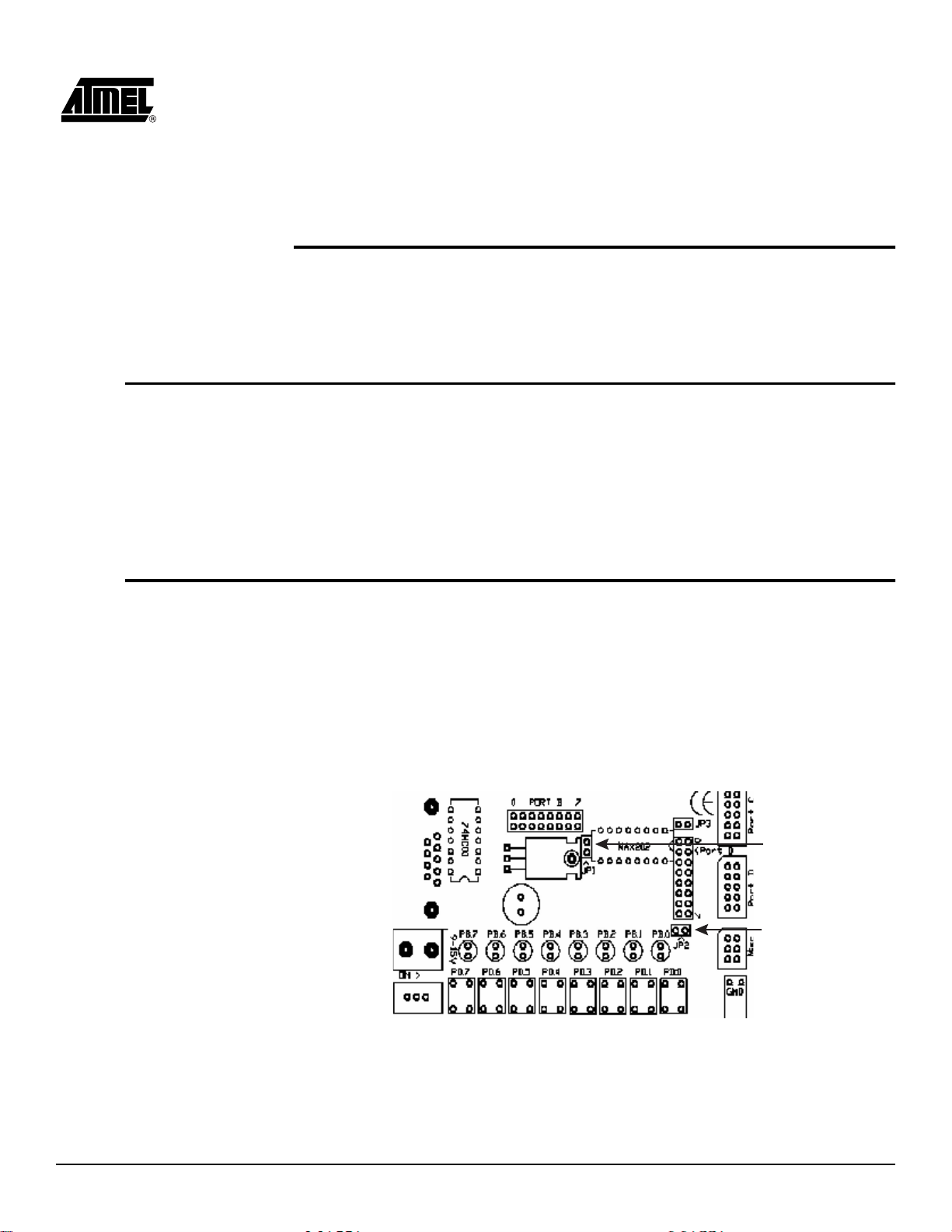
The LEDs are connected through a 1K resistor network to Port B.
The switches are connected to Port D.
The switches an d LE Ds can be di sco nnecte d, if requir ed. To use them, ens ure that th e
jumpers labeled “Port B” and “Port D” are closed. The board is also marked with the port
pin connection for each switch and LED.
The ports must be correctly set in software as input or output. This is accomplished by
setting the direction control r egister s to 0 for i nput and 1 for output. Ty pica l set-up c ode
would be:
ldi r16,$ff ;move immediate into temporary store register
out DDRB,r16 ;set direction register to ones for output -
LEDs
out PORTB,r16 ;switch all the LEDs on
ldi r16,$00 ;move immediate into temporary store register
out DDRD,r16 ;set direction register to zeros for input
Switches
All the ports are brought out to headers on the edge of the boar d. In additi on to the port
pins, each header has a connection for ground and V
this voltage, V
and the brown-out detector will operate.
Note:
If your circuit is to draw significant current (>150 mA) then a heat sink will be
required on the on-board regulator—LM317. This device is rated at 1.5 amps
but it does need a heat sink to supply this current. If your circuit will draw more
than 1 amp, you may need a separate power supply. The ports on the device
are connected to the headers marked Port A, Port B, Port C, Port D, Port E and
Analog, Port F. The layout of all the headers is the same and is shown in the following diagram.
, will be either 3.3V or 5V depending on the setti ng of jumper 1, JP1,
CC
to supply external circuits. Note
CC
megaAVR™ Starter Kit Manual 9-1

Board Applications
CUT CORNER
SHOWN ON BOARD
FOR ORIENTATION
BIT 0 OF PORT.
SAME FOR ALL PORTS
BIT 7 OF PORT.
SAME FOR ALL PORTS
9.2.1 Misc. Header
9.3 Using Analog Functions
EXTRA CONNECTION
FOR GROUND
EXTRA CONNECTION
FOR V
CC
The last header labeled “Misc.” has con nections to processor pins other tha n the
port pins.
CUT OUT MARKED
ON BOARD
FOR ORIENTATION
READ
RD
WRITE
WR
EXTRA CONNECTION
FOR GROUND
EXTRA CONNECTION
FOR V
CC
If external operat ions do not wan t pull-up s on the port pin , both the swit ches and the
LEDs can be disconnected from the processor. To isolate the LEDs, remove the jumper
set labeled “Port B”, and to isolate the switches, remove the jumper set labeled “Port D”.
The A/D converters use the head er labele d “A nal og ” for the A/D in puts on Po rt F, whic h
is input only. A +10V to -10V supply is provided on the connector marked “Op-Amp” next
to the crystal. A lead from this connector can be used for an external amp lifier for th e
A/D inputs. The layout of the Analog header is shown below.
9.3.1 Analog Port: Marked on Board
ADC0 - ADC7 CONNECTED
CUT OUT MARKED
ON BOARD
FOR ORIENTATION
TO PORT FPF0 - PF7
The A/D converters can use either the on-boar d (Internal) Voltage Reference or an
external Voltage Reference.
9.3.2 Using Internal Reference
To use the internal, on-boa rd Vo ltage Re ference, the pot m arked “ AREF” is used to set
the voltage lev el. The vo ltage le vel can be measur ed with a D VM connec ted to the
9-2 megaAVR™ Starter Kit Manual

Board Applications
1
2
3
4
5
6
7
8
9
10
11
12
13
14
28
27
26
25
24
23
22
21
20
19
18
17
16
15
A14
A12
A7
A6
A5
A4
A3
A2
A1
A0
I/O0
I/O1
I/O2
VSS
VCC
WE
A13
A8
A9
A11
OE
A10
CS
I/O7
I/O6
I/O5
I/O4
I/O3
header pins labeled “A nal og Ref” and “Analog Gnd” in the pr evio us dia gr am o r fro m th e
two holes marked Meter + and -.
9.3.3 Using External Reference
9.4 Using External RAM
9.4.1 RAM Recommendations
9.4.2 RAM Socket Pin Layout
To use the A/D converters with an external Voltag e Reference, the li nk marked “LK1”
must be cut. The voltage is applied to the pins marked “Analog Ref” and “Analog Gnd”
on the Analog header—see previous diagram.
The ATmega103 can be used with external SRAM. A socket is provided for a 28-pin
RAM chip and for an address latch chip. These are next to the device adapter at the top
of the board. There is also a he ader for furt her mem ory expan sion, whi ch is conn ected
through the address latc h. The pin functi ons are marked on the board, includi ng chip
select (CS).
A low power 62256 SRAM is suggested with an access time of 70 nS. If a very fast RAM
is required, the crys tal frequ ency may nee d to be incre ased. If a muc h slower SRAM is
used, the SRAM Wait State bit must be enabled in user software–—see data book. The
layout of the 28-pin RAM socket is shown below, and any RAM with this pin-out could
be used.
9.4.3 Address Latch
The board connections ar e for a 74HC573 device. This dev ice will ope rate reliab ly with
the 4 MHz cr ystal su pplied but i f a faster crystal is ins erted, a f aster ver sion of th is
device may be required—74AHC573 or 74FHC573. Note that this option will alter the
EMC characteristics of the board and the CE mark will no longer be valid
without retesting.
9.5 Using LCD Connections
megaAVR™ Starter Kit Manual 9-3
The header marked LCD interf ace is for a standard 2 x 16 LCD. The c onnections are
shown on the board and in the following table.
Connection Name Function
0V Ground
+5 V
Vo Contrast
RS Register Select- A14
Wr Not Write
EEnable
D0 Data Bit 0
- must be 5V
CC

Board Applications
Connection Name Function
D1 Data Bit 1
D2 Data Bit 2
D3 Data Bit 3
D4 Data Bit 4
D5 Data Bit 5
D6 Data Bit 6
D7 Data Bit 7
The board is designed for use with a LCD with a Hitachi driver chip built-in, with a contrast pin voltage of 0 to 5 Volts. The pot next to the LCD connector is used for contrast
adjustment.
If you use a different LCD driver, it may have a different voltage contrast range. In order
to accommodate this, add a resistor to the board (shown on board) and cut track on
underside of board—marked cut.
This board is not designed for use with back lit LCD modules , so the extra c onnections
needed are not included and the power supply will not supply the current required.
The LCD must be driven in Memory Mappe d Mode as Read and Wri te are descite pins
on the Mega parts—see data sheet. If the crystal has been changed to a faster crystal
frequency, memory mapped operations will not work.
9.6 Using RS232
9.7 Programming InSystem
The connection supplied is a 9-way female D-type, so a straight-through lead is
required, not a null-modem cable.
The Jumpers in the middle of the board, marked PE0 and PE1 must be set to RS232,
not Port or RXD and TXD will be disabled.
As this board has a 4 MHz crystal , the percentage error on the Baud Rate will be
between 0.2 and 7.8%. Replacing the crystal with a 3.6846 MHz or 4.608 MHz crystal
will reduce this error to zero but may have EMC implications.
A standard (straight-through) lead is required, NOT a null-modem cable.
Devices can be programmed in your circuit rather than on the board.
For In-System Programming , ISP, the 10- conduc tor ribbon cable is co nnecte d to a dual
row 10-pin 0.1" pitch header on your circuit.
You will need to use either a multiplexer chip, such as a 4053, or wire directly to the pins
of the device. Without a multipl exer chip , Serial Co mmunications and SPI por t will b e
unusable.
In addition, the syste m 5 Volts an d Ground nee ds to be connec ted to the pr ogrammin g
lead.
DO NOT EXCEED 5 VOLTS ± 5% (4.75V TO 5.25V). YOU MAY DAMAGE YOUR
COMPUTER. THIS WARNING APPLIES TO ANY ISP SYSTEM.
9-4 megaAVR™ Starter Kit Manual

9.8 ISP Header Layout
9.9 Interface Using Resistors
Board Applications
KEY WAY
OPTIONAL PROGRAM
INDICATOR CICRUIT
PROGRAMMING HEADER MISO IS CALLED PDO AND
MOSI IS PDI ON MEGA
DEVICES - PORT E BITS 0 AND 1
NOT PINS ON PORT B.
9.10 Using an Analogue Multiplexer IC
USER
CIRCUIT
Typical resistor values would be 1K. This circuit is fine if ports PB7, PE0 and PE1 are
used as inputs in your circuit and no communication is required. If Outputs are needed
or RS232 connections , especiall y higher than a few mill iamps, th en the multipl exed circuit is preferable.
TO ISP
CONNECTOR
TO USER
CIRCUIT
The multiplexer select can be driven from the LED connection on the programming lead,
as can a low power LED with its cathode connected to the LED connection via a suitable
resistor. 1KΩ is fine. If you use this connectio, then the output will be low 0 during programming and a 1 at all other times. Note that it will float if the programmer is not active,
i.e., the software is not running, so you may need to use a pull-up resistor.
megaAVR™ Starter Kit Manual 9-5

Board Applications
9.10.1 Using Real Time Clock
Note:
A 32.768 kHz crystal is connected to TOSC1 and TOSC2 pins—Pin 18 and Pin 19. This
can be used to generate a 1 second pulse—see data book for details.
All the pins except ground will float if the programmer is not active. The device
may then be programmed in the normal way.
9-6 megaAVR™ Starter Kit Manual

Board Applications
Lights and Switches
VCC
P-RESET
VCC
10K
Resnet
Active 0 on LEDs
PB0
PB1
PB2
PB3
PB4
PB5
PB6
PB7
EXT RESET
RESET
R12
10K
Q2
BC182
123
R14
1M
R11
10K
Q1
BC182
123
MEGA Pin 3 ( PE1)
MEGA Pin 11 (SCK
MEGA Pin 2 ( PE0)
4
15
X14Y
Z
X012X113Y02Y11Z05Z13INH6A11B10C
U2
1K
1K
R13
R16
PORT B Bit 1
9
4053
PORT PIN
PE1
RS 232
PORT PIN
PE0
RS 232RST + BROWNOUT
Brow nout Detector Circuit
C7
5V Brownout
LCD Interface
100nF
MOSI (ISP)
SCK (ISP)
R9
11K
R10
18K
Data 7
Data 6
Data 5
Data 4
Data 3
Data 2
Data 1
Data 0
Enable
R/W
Reg Sel
Cont
+5V
GND
MOSI (ISP)
PB0
Pro gramming Interface
+5
14
13
12
11
10
9
8
7
6
5
4
3
2
1
100R
+5
LED Enable ( ISP)
1 2
3 4
5 6
7 8
9 10
ISP LED
ISP RST
ISP MOSI
HEADER 5X2
ISP SCK
3
+5
1K
R2
ISP MISO
BRIDGE
BC212
1
2
1K
R1
RST (ISP)
External Power Source
(DC or AC)
S1
SW SPST
-+
R8
43K
1 2
3 4
5 6
7 8
9 10
11 12
13 14
15 16
HEADER 8X2
PB0
PB1
PB2
PB3
PB4
PB5
PB6
PB7
VCC
PD0
10K
Resnet
PD3
PD4
PD2
PD1
PD7
PD5
PD6
Active 0 on Switches
1 2
3 4
5 6
7 8
9 10
11 12
13 14
15 16
HEADER 8X2
PD0
PD1
PD2
PD3
PD4
PD5
PD6
PD7
C19
100nF
VCC
C18
100nF
C17
100nF
C16
100nF
C15
100nF
C14
100nF
C13
100nF
VREF
C20
VR1
10K
VCC
Analogue Reference Decoupling Capacitors
100nF
AGND
P9
594837261
+5V+5V
16
15
RS232 Circuit
Vcc
C1+1V+2C1-3C2+4C2-5V-6T2OUT7R2IN
U4
-10V
+10V
GND
14
13
T1OUT
C10
+
C9
+
C12
+
C11
+
R1IN
12
10uF
10uF
10uF
10uF
11
R1OUT
T2IN10T1IN
9
8
R2OUT
RS232
MAX202CPE
TXD
RXD
EN
U3C
9
R3
10K
+5
C8
11
U3D
LCD Timing Ciruit
12
A15
8
74HC00
10
33pF
74HC00
13
BAT85
D2
CS
3
U3A
74HC00
1
2
2
VOUT
6 R15
U3B
74HC00
4
5
WR
RD
REG1
LM317T
3
VIN
VCC
REG2
ADJ
1
R6
240R
C3
220uF
1
VOUT
GND
2
VIN
LM78L05ACH
3
C4
470nF
+5
C6
100nf
R5
39R
R4
680R
R7
820R
3V3
C5
470nF
GND GND AGND
9-7 megaAVR™ Starter Kit Manual

Board Applications
megaAVR™ Starter Kit Manual 9-8

Board Applications
9-9 megaAVR™ Starter Kit Manual

Atmel Headquarters Atmel Operations
Corporate Headquarters
2325 Orchard Parkway
San Jose, CA 95131
TEL (408) 441- 0311
FAX (408) 487-2600
Europe
Atmel U.K., Ltd.
Coliseum Business Centre
Riverside Way
Camberley, Surrey GU15 3YL
England
TEL (44) 1276-686677
FAX (44) 1276-686697
Asia
Atmel Asia, Ltd.
Room 1219
Chinachem Golden Plaza
77 Mody Road
Tsimshatsui East
Kowloon, Hong Kong
TEL (852) 27219778
FAX (852) 27221369
Japan
Atmel Japan K.K.
Tonetsu Shinkawa Bldg., 9F
1-24-8 Shinka wa
Chuo-ku, Tokyo 104-0033
Japan
TEL (81) 3-3523-3551
FAX (81) 3-3523-7581
Atmel Colorado Springs
1150 E. Cheyenne Mtn. Blvd.
Colorado Springs, CO 80906
TEL (719) 576-3300
FAX (719) 540-1759
Atmel Rousset
Zone Indu strie lle
13106 Rousset Cedex, France
TEL (33) 4 42 53 60 00
FAX (33) 4 42 53 60 01
Fax-on-Demand
North America:
1-(800) 292-8635
International:
1-(408) 441-0732
e-mail
literature@atmel.com
Web Site
http://www.atmel.com
BBS
1-(408) 436-4309
© Atmel Corporation 1998.
Atmel Corporation makes no warranty for the use of its products, other than those expressly contained in the Company’s standard warranty which is detailed in Atmel’s Terms and Conditions located on the Company’s web site. The Company assumes no responsibility for
any errors which may appear in this document, reserves the right to change devices or specifications detailed herein at any time without
notice, and does not make any commitment to update the information contained herein. No licenses to patents or other intellectual property of Atmel are granted by the Company in connection with the sale of Atmel products, expressly or by implication. Atmel’s products are
not authorized for use as critical components in life support devices or systems.
Marks bearing ® and/or ™ are registered trademarks and trademarks of Atmel Corporation.
Terms and product names in this document may be trademarks of others.
Printed on recycled paper.
1149A–02/99/2M
 Loading...