


This document contains complete and detailed description of all modules included in
the Atmel
family of low-power, high-performance, and peripheral-rich CMOS 8/16-bit microcontrollers based on the AVR enhanced RISC architecture. The available Atmel AVR
XMEGA AU modules described in this manual are:
•
Atmel AVR CPU
• Memories
• DMAC - Direct memory access controller
• Event system
• System clock and clock options
• Power management and sleep modes
• System control and reset
• Battery backup system
• WDT - Watchdog timer
• Interrupts and programmable multilevel interrupt controller
• PORT - I/O ports
• TC - 16-bit timer/counters
• AWeX - Advanced waveform extension
• Hi-Res - High resolution extension
• RTC - Real-time counter
• RTC32 - 32-bit real-time counter
• USB - Universial serial bus interface
• TWI - Two-wire serial interface
• SPI - Serial peripheral interface
• USART - Universal synchronous and asynchronous serial receiver and transmitter
• IRCOM - Infrared communication module
• AES and DES cryptographic engine
• CRC - Cyclic redundancy check
• EBI - External bus interface
• ADC - Analog-to-digital converter
• DAC - Digital-to-analog converter
• AC - Analog comparator
• IEEE 1149.1 JTAG interface
• PDI - Program and debug interface
• Memory programming
• Peripheral address map
• Register summary
• Interrupt vector summary
• Instruction set summary
®
AVR®XMEGA®AU microcontroller family. The Atmel AVR XMEGA AU is a
8-bit Atmel
XMEGA AU
Microcontroller
XMEGA AU
MANUAL
8331B- AVR-03/12

1. About the Manual
This document contains in-depth documentation of all peripherals and modules available for the
Atmel AVR XMEGA AU microcontroller family. All features are documented on a functional level
and described in a general sense. All peripherals and modules described in this manual may not
be present in all Atmel AVR XMEGA AU devices.
For all device-specific information such as characterization data, memory sizes, modules,
peripherals available and their absolute memory addresses, refer to the device datasheets.
When several instances of a peripheral exists in one device, each instance will have a unique
name. For example each port module (PORT) have unique name, such as PORTA, PORTB,etc.
Register and bit names are unique within one module instance.
For more details on applied use and code examples for peripherals and modules, refer to the
Atmel AVR XMEGA specific application notes available from http://www.atmel.com/avr.
1.1 Reading the Manual
The main sections describe the various modules and peripherals. Each section contains a short
feature list and overview describing the module. The remaining section describes the features
and functions in more detail.
Atmel AVR XMEGA AU
The register description sections list all registers and describe each register, bit and flag with
their function. This includes details on how to set up and enable various features in the module.
When multiple bits are needed for a configuration setting, these are grouped together in a bit
group. The possible bit group configurations are listed for all bit groups together with their associated Group Configuration and a short description. The Group Configuration refers to the
defined configuration name used in the Atmel AVR XMEGA assembler header files and application note source code.
The register summary sections list the internal register map for each module type.
The interrupt vector summary sections list the interrupt vectors and offset address for each module type.
1.2 Resources
A comprehensive set of development tools, application notes, and datasheets are available for
download from http://www.atmel.com/avr.
1.3 Recommended Reading
• Atmel AVR XMEGA AU device datasheets
• XMEGA application notes
This manual contains general modules and peripheral descriptions. The AVR XMEGA AU device
datasheets contains the device-specific information. The XMEGA application notes and AVR
Software Framework contain example code and show applied use of the modules and peripherals.
8331B–AVR–03/12
For new users, it is recommended to read the AVR1000 - Getting Started Writing C Code for
Atmel XMEGA, and AVR1900 - Getting Started with Atmel ATxmega128A1 application notes.
2

2. Overview
Atmel AVR XMEGA AU
The AVR XMEGA AU microcontrollers is a family of low-power, high-performance, and peripheral-rich CMOS 8/16-bit microcontrollers based on the AVR enhanced RISC architecture. By
executing powerful instructions in a single clock cycle, the Atmel AVR XMEGA AU devices
achieve throughputs approaching one million instructions per second (MIPS) per megahertz,
allowing the system designer to optimize power consumption versus processing speed.
The AVR CPU combines a rich instruction set with 32 general purpose working registers. All 32
registers are directly connected to the arithmetic logic unit (ALU), allowing two independent registers to be accessed in a single instruction, executed in one clock cycle. The resulting
architecture is more code efficient while achieving throughputs many times faster than conventional single-accumulator or CISC based microcontrollers.
The Atmel AVR XMEGA AU devices provide the following features: in-system programmable
flash with read-while-write capabilities; internal EEPROM and SRAM; four-channel DMA controller; eight-channel event system and programmable multilevel interrupt controller; up to 78
general purpose I/O lines; 16- or 32-bit real-time counter (RTC); up to eight flexible, 16-bit
timer/counters with capture, compare and PWM modes; up to eight USARTs; up to four I
SMBUS compatible two-wire serial interfaces (TWIs); one full-speed USB 2.0 interface; up to
four serial peripheral interfaces (SPIs); CRC module; AES and DES cryptographic engine; up to
two 16-channel, 12-bit ADCs with programmable gain; up to two 2-channel, 12-bit DACs; up to
four analog comparators with window mode; programmable watchdog timer with separate internal oscillator; accurate internal oscillators with PLL and prescaler; and programmable brown-out
detection.
2
C and
The program and debug interface (PDI), a fast, two-pin interface for programming and debugging, is available. Selected devices also have an IEEE std. 1149.1 compliant JTAG interface,
and this can also be used for on-chip debug and programming.
The Atmel AVR XMEGA devices have five software selectable power saving modes. The idle
mode stops the CPU while allowing the SRAM, DMA controller, event system, interrupt controller, and all peripherals to continue functioning. The power-down mode saves the SRAM and
register contents, but stops the oscillators, disabling all other functions until the next TWI, USB
resume, or pin-change interrupt, or reset. In power-save mode, the asynchronous real-time
counter continues to run, allowing the application to maintain a timer base while the rest of the
device is sleeping. In standby mode, the external crystal oscillator keeps running while the rest
of the device is sleeping. This allows very fast startup from the external crystal, combined with
low power consumption. In extended standby mode, both the main oscillator and the asynchronous timer continue to run. To further reduce power consumption, the peripheral clock to each
individual peripheral can optionally be stopped in active mode and idle sleep mode.
The devices are manufactured using Atmel high-density, nonvolatile memory technology. The
program flash memory can be reprogrammed in-system through the PDI or JTAG interfaces. A
boot loader running in the device can use any interface to download the application program to
the flash memory. The boot loader software in the boot flash section will continue to run while
the application flash section is updated, providing true read-while-write operation. By combining
an 8/16-bit RISC CPU with In-system, self-programmable flash, the Atmel AVR XMEGA is a
powerful microcontroller family that provides a highly flexible and cost effective solution for many
embedded applications.
8331B–AVR–03/12
3
The Atmel AVR XMEGA AU devices are supported with a full suite of program and system
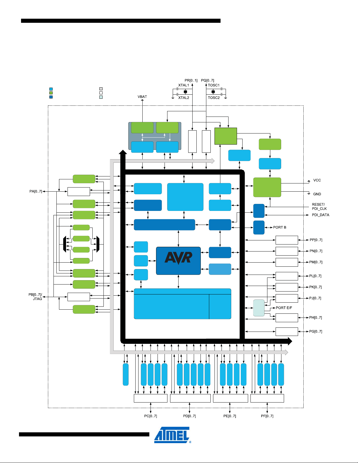
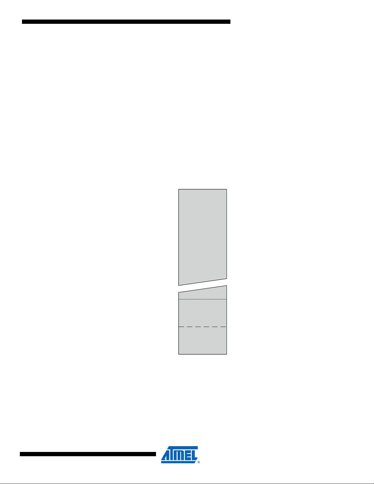
V
BAT
Power
Supervision
Battery Backup
Controller
Real Time
Counter
32.768 kHz
XOSC
Power
Supervision
POR/BOD &
RESET
PORT A (8)
PORT B (8)
EVENT ROUTING NETWORK
DMA
Controller
BUS
Matrix
SRAM
EBI
ADCA
DACA
ACA
DACB
ADCB
ACB
OCD
PORT K (8)
PORT J (8)
PORT H (8)
PDI
Watchdog
Timer
Watchdog
Oscillator
Interrupt
Controller
DATA BUS
Prog/Debug
Controller
PORT R (2)
Oscillator
Circuits/
Clock
Generation
Oscillator
Control
Real Time
Counter
Event System
Controller
JTAG
Sleep
Controller
DES
CRC
IRCOM
PORT G (8)
PORT L (8)
PORT Q (8)
PORT M (8)
PORT C (8)
TCC0:1
USARTC0:1
TWIC
SPIC
PORT D (8)
TCD0:1
USARTD0:1
TWID
SPID
TCF0:1
USARTF0:1
TWIF
SPIF
TCE0:1
USARTE0:1
TWIE
SPIE
PORT E (8) PORT F (8)
USB
EVENT ROUTING NETWORK
AES
AREFA
AREFB
PORT N (8)
PORT P (8)
CPU
NVM Controller
MORPEEhsalF
DATA BUS
Int. Refs.
Tempref
Digital function
Analog function
Bus masters / Programming / Debug
Oscillator / Crystal / Clock
General Purpose I/O
EBI
development tools, including C compilers, macro assemblers, program debugger/simulators,
programmers, and evaluation kits.Block Diagram
Figure 2-1. Atmel AVR XMEGA AU block diagram.
Atmel AVR XMEGA AU
8331B–AVR–03/12
4
Atmel AVR XMEGA AU
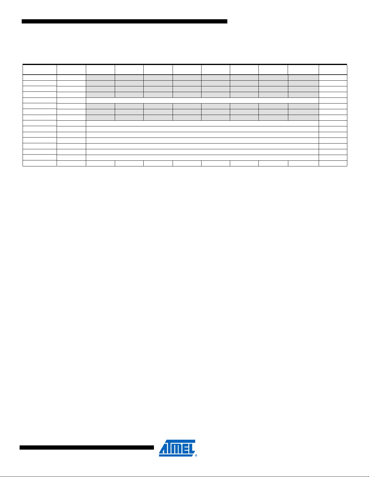
In Table 2-1 on page 5 a feature summary for the XMEGA AU family is shown, split into one feature summary column for each sub-family. Each sub-family has identical feature set, but different
memory options, refer to their device datasheet for ordering codes and memory options.
Table 2-1. XMEGA AU feature summary overview.
Feature Details / sub-family A1U A3U A3BU A4U
Pins, I/O
Memory
Package
QTouch Sense channels 56 56 56 56
DMA Controller Channels 4 4 4 4
Event System
Crystal Oscillator
To t al 100 64 64 44
Programmable I/O pins 78 50 47 34
Program memory (KB) 64 - 128 64 - 256 256 16 - 128
Boot memory (KB) 4 - 8 4 - 8 8 4 - 8
SRAM (KB) 4 - 8 4 - 16 16 2 - 8
EEPROM 2 2 - 4 4 1 -2
General purpose registers 16 16 16 16
TQFP 100A 64A 64A 44A
QFN /VQFN – 64M2 64M2 44M1
BGA 100C1/100C2 – – 49C2
Channels 8 8 8 8
QDEC 3 3 3 3
0.4 - 16MHz XOSC Yes Ye s Yes Ye s
32.768 kHz TOSC Yes Yes Ye s Yes
2MHz calibrated Yes Ye s Yes Ye s
32MHz calibrated Yes Ye s Yes Ye s
Internal Oscillator
Timer / Counter
Battery Backup System Yes
8331B–AVR–03/12
128MHz PLL Yes Ye s Yes Ye s
32.768kHz calibrated Yes Yes Yes Ye s
32kHz ULP Yes Yes Yes Yes
TC0 - 16-bit, 4 CC 4 4 4 3
TC1 - 16-bit, 2 CC 4 3 2 2
TC2 - 2x 8-bit 4 4 4 2
Hi-Res 4 4 4 3
AWeX 4 2 2 1
RTC 1 1 1
RTC32 1
5
Atmel AVR XMEGA AU
Feature Details / sub-family A1U A3U A3BU A4U
USB full-speed device 1 1 1 1
Serial Communication
Crypto /CRC
External Memory (EBI)
Analog to Digital
Converter (ADC)
USART 8 7 6 5
SPI 4 3 3 2
TWI 4 2 2 2
AES-128 Yes Ye s Yes Ye s
DES Yes Ye s Yes Ye s
CRC-16 Ye s Yes Ye s Yes
CRC-32 Ye s Yes Ye s Yes
Chip selects 4 – – –
SRAM Yes
SDRAM Ye s
2 2 2 1
Resolution (bits) 12 12 12 12
Sampling speed (kbps) 2000 2000 2000 2000
Input channels per ADC 16 16 16 12
Conversion channels 4 4 4 4
2 1 1 1
Digital to Analog
Converter (DAC)
Analog Comparator (AC) 4 4 4 2
Program and Debug
Interface
Resolution (bits) 12 12 12 12
Sampling speed (kbps) 1000 1000 1000 1000
Output channels per DAC 2 2 2 2
PDI Yes Ye s Yes Ye s
JTAG Ye s Yes Yes
Boundary scan Yes Ye s Yes
8331B–AVR–03/12
6
3. AVR CPU
3.1 Features
3.2 Overview
Atmel AVR XMEGA AU
• 8/16-bit, high-performance Atmel AVR RISC CPU
– 142 instructions
– Hardware multiplier
• 32x8-bit registers directly connected to the ALU
• Stack in RAM
• Stack pointer accessible in I/O memory space
• Direct addressing of up to 16MB of program memory and 16MB of data memory
• True 16/24-bit access to 16/24-bit I/O registers
• Efficient support for 8-, 16-, and 32-bit arithmetic
• Configuration change protection of system-critical features
All Atmel AVR XMEGA devices use the 8/16-bit AVR CPU. The main function of the CPU is to
execute the code and perform all calculations. The CPU is able to access memories, perform
calculations, control peripherals, and execute the program in the flash memory. Interrupt handling is described in a separate section, ”Interrupts and Programmable Multilevel Interrupt
Controller” on page 134.
3.3 Architectural Overview
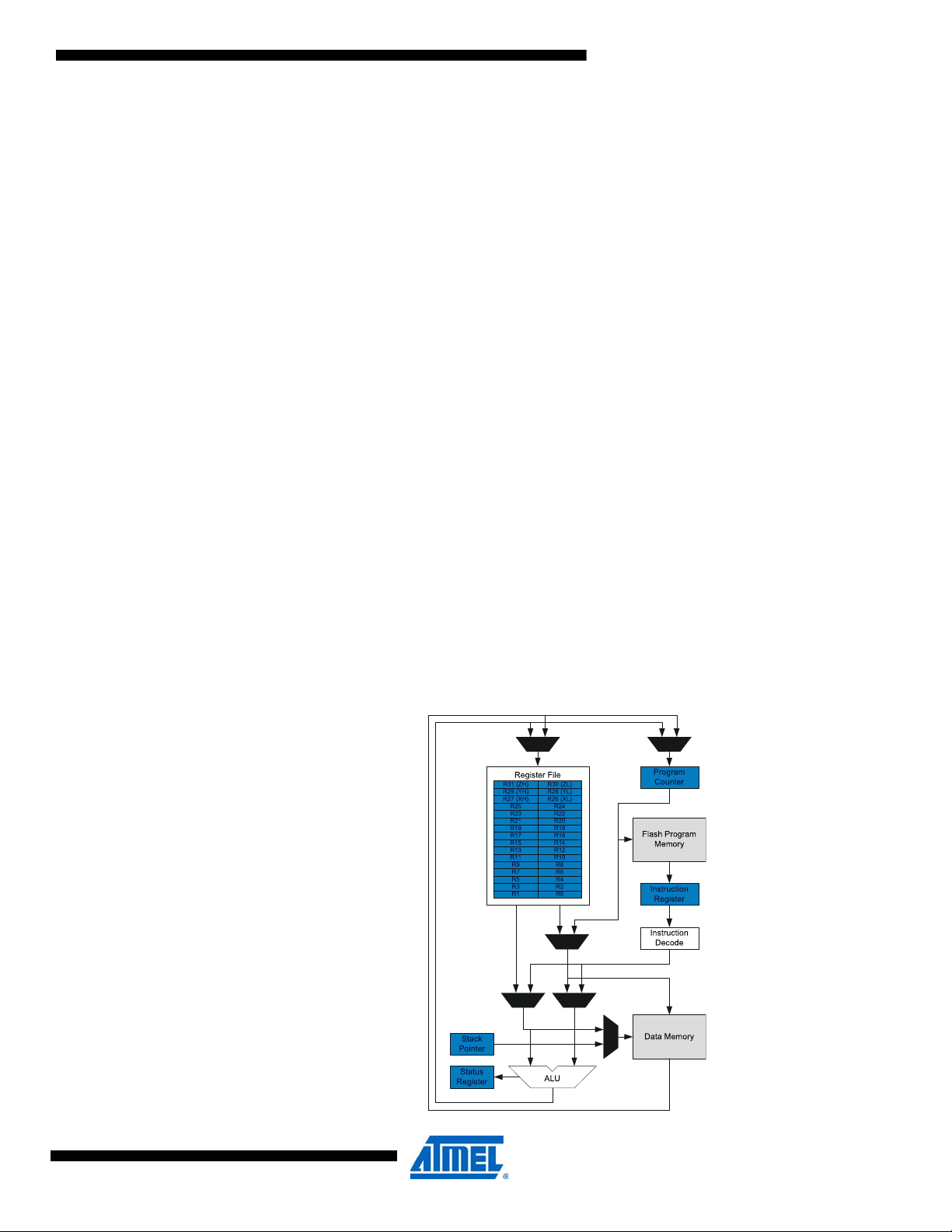
In order to maximize performance and parallelism, the AVR CPU uses a Harvard architecture
with separate memories and buses for program and data. Instructions in the program memory
are executed with single-level pipelining. While one instruction is being executed, the next
instruction is pre-fetched from the program memory. This enables instructions to be executed on
every clock cycle. For a summary of all AVR instructions, refer to ”Instruction Set Summary” on
page 456. For details of all AVR instructions, refer to http://www.atmel.com/avr.
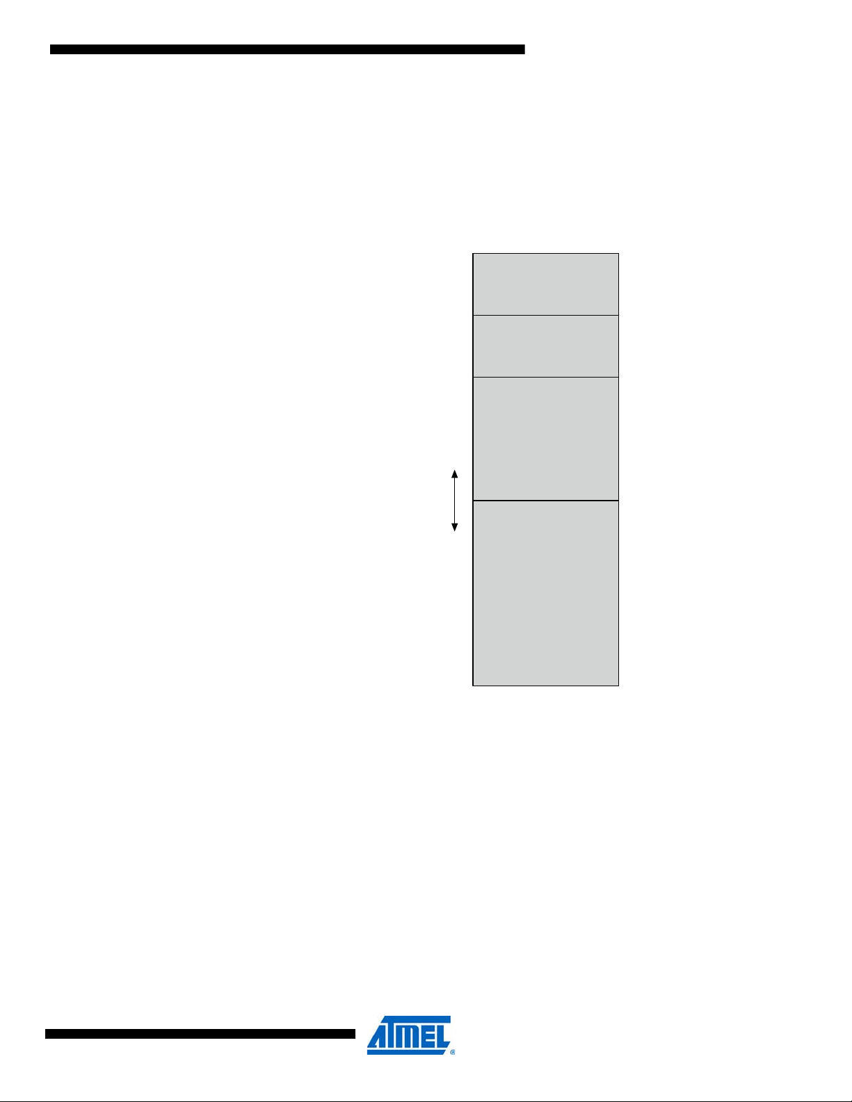
Figure 3-1. Block diagram of the AVR CPU architecture.
8331B–AVR–03/12
7

Atmel AVR XMEGA AU
The arithmetic logic unit (ALU) supports arithmetic and logic operations between registers or
between a constant and a register. Single-register operations can also be executed in the ALU.
After an arithmetic operation, the status register is updated to reflect information about the result
of the operation.
The ALU is directly connected to the fast-access register file. The 32 x 8-bit general purpose
working registers all have single clock cycle access time allowing single-cycle arithmetic logic
unit operation between registers or between a register and an immediate. Six of the 32 registers
can be used as three 16-bit address pointers for program and data space addressing, enabling
efficient address calculations.
The memory spaces are linear. The data memory space and the program memory space are
two different memory spaces.
The data memory space is divided into I/O registers, SRAM, and external RAM. In addition, the
EEPROM can be memory mapped in the data memory.
All I/O status and control registers reside in the lowest 4KB addresses of the data memory. This
is referred to as the I/O memory space. The lowest 64 addresses can be accessed directly, or as
the data space locations from 0x00 to 0x3F. The rest is the extended I/O memory space, ranging
from 0x0040 to 0x0FFF. I/O registers here must be accessed as data space locations using load
(LD/LDS/LDD) and store (ST/STS/STD) instructions.
The SRAM holds data. Code execution from SRAM is not supported. It can easily be accessed
through the five different addressing modes supported in the AVR architecture. The first SRAM
address is 0x2000.
Data addresses 0x1000 to 0x1FFF are reserved for memory mapping of EEPROM.
The program memory is divided in two sections, the application program section and the boot
program section. Both sections have dedicated lock bits for write and read/write protection. The
SPM instruction that is used for self-programming of the application flash memory must reside in
the boot program section. The application section contains an application table section with separate lock bits for write and read/write protection. The application table section can be used
forsave storing of nonvolatile data in the program memory.
3.4 ALU - Arithmetic Logic Unit
The arithmetic logic unit supports arithmetic and logic operations between registers or between
a constant and a register. Single-register operations can also be executed. The ALU operates in
direct connection with all 32 general purpose registers. In a single clock cycle, arithmetic operations between general purpose registers or between a register and an immediate are executed
and the result is stored in the register file. After an arithmetic or logic operation, the status register is updated to reflect information about the result of the operation.
ALU operations are divided into three main categories – arithmetic, logical, and bit functions.
Both 8- and 16-bit arithmetic is supported, and the instruction set allows for efficient implementation of 32-bit aritmetic. The hardware multiplier supports signed and unsigned multiplication and
fractional format.
8331B–AVR–03/12
8
3.4.1 Hardware Multiplier
The multiplier is capable of multiplying two 8-bit numbers into a 16-bit result. The hardware multiplier supports different variations of signed and unsigned integer and fractional numbers:
• Multiplication of unsigned integers
• Multiplication of signed integers
• Multiplication of a signed integer with an unsigned integer
• Multiplication of unsigned fractional numbers
• Multiplication of signed fractional numbers
• Multiplication of a signed fractional number with an unsigned one
A multiplication takes two CPU clock cycles.
3.5 Program Flow
After reset, the CPU starts to execute instructions from the lowest address in the flash programmemory ‘0.’ The program counter (PC) addresses the next instruction to be fetched.
Program flow is provided by conditional and unconditional jump and call instructions capable of
addressing the whole address space directly. Most AVR instructions use a 16-bit word format,
while a limited number use a 32-bit format.
Atmel AVR XMEGA AU
During interrupts and subroutine calls, the return address PC is stored on the stack. The stack is
allocated in the general data SRAM, and consequently the stack size is only limited by the total
SRAM size and the usage of the SRAM. After reset, the stack pointer (SP) points to the highest
address in the internal SRAM. The SP is read/write accessible in the I/O memory space,
enabling easy implementation of multiple stacks or stack areas. The data SRAM can easily be
accessed through the five different addressing modes supported in the AVR CPU.
3.6 Instruction Execution Timing
The AVR CPU is clocked by the CPU clock, clk
on page 9 shows the parallel instruction fetches and instruction executions enabled by the Har-
vard architecture and the fast-access register file concept. This is the basic pipelining concept
used to obtain up to 1MIPS/MHz performance with high power efficiency.
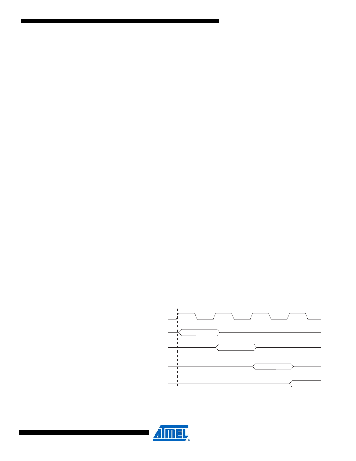
Figure 3-2. The parallel instruction fetches and instruction executions.
1st Instruction Fetch
1st Instruction Execute
2nd Instruction Fetch
2nd Instruction Execute
3rd Instruction Fetch
clk
CPU
. No internal clock division is used. Figure 3-2
CPU
T1 T2 T3 T4
8331B–AVR–03/12
3rd Instruction Execute
4th Instruction Fetch
9
Atmel AVR XMEGA AU
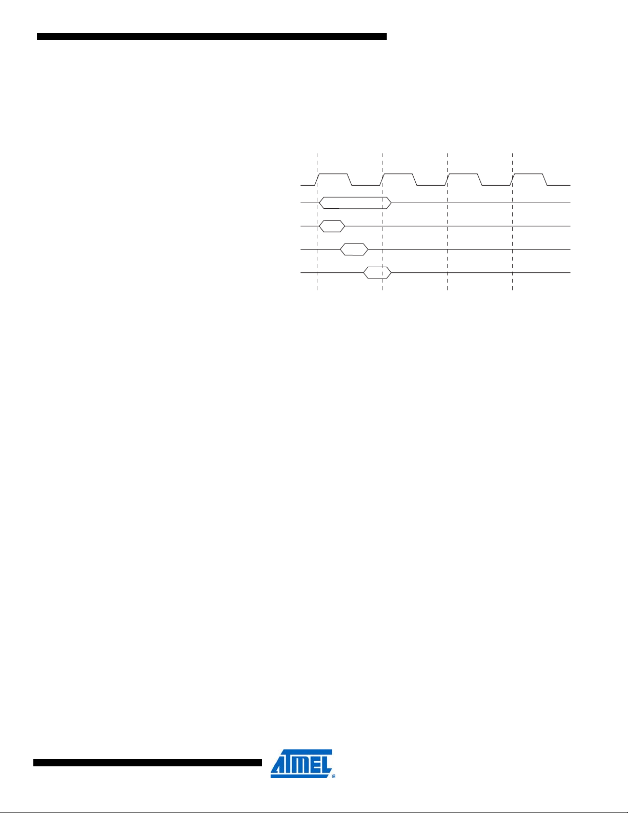
Total Execution Time
Register Operands Fetch
ALU Operation Execute
Result Write Back
T1 T2 T3 T4
clk
CPU
Figure 3-3 on page 10 shows the internal timing concept for the register file. In a single clock
cycle, an ALU operation using two register operands is executed and the result is stored back to
the destination register.
Figure 3-3. Single Cycle ALU Operation
3.7 Status Register
The status register (SREG) contains information about the result of the most recently executed
arithmetic or logic instruction. This information can be used for altering program flow in order to
perform conditional operations. Note that the status register is updated after all ALU operations,
as specified in the instruction set reference. This will in many cases remove the need for using
the dedicated compare instructions, resulting in faster and more compact code.
The status register is not automatically stored when entering an interrupt routine nor restored
when returning from an interrupt. This must be handled by software.
The status register is accessible in the I/O memory space.
3.8 Stack and Stack Pointer
The stack is used for storing return addresses after interrupts and subroutine calls. It can also be
used for storing temporary data. The stack pointer (SP) register always points to the top of the
stack. It is implemented as two 8-bit registers that are accessible in the I/O memory space. Data
are pushed and popped from the stack using the PUSH and POP instructions. The stack grows
from a higher memory location to a lower memory location. This implies that pushing data onto
the stack decreases the SP, and popping data off the stack increases the SP. The SP is automatically loaded after reset, and the initial value is the highest address of the internal SRAM. If
the SP is changed, it must be set to point above address 0x2000, and it must be defined before
any subroutine calls are executed or before interrupts are enabled.
During interrupts or subroutine calls, the return address is automatically pushed on the stack.
The return address can be two or three bytes, depending on program memory size of the device.
For devices with 128KB or less of program memory, the return address is two bytes, and hence
the stack pointer is decremented/incremented by two. For devices with more than 128KB of program memory, the return address is three bytes, and hence the SP is decremented/incremented
by three. The return address is popped off the stack when returning from interrupts using the
RETI instruction, and from subroutine calls using the RET instruction.
8331B–AVR–03/12
10

3.9 Register File
Atmel AVR XMEGA AU
The SP is decremented by one when data are pushed on the stack with the PUSH instruction,
and incremented by one when data is popped off the stack using the POP instruction.
To prevent corruption when updating the stack pointer from software, a write to SPL will automatically disable interrupts for up to four instructions or until the next I/O memory write.
The register file consists of 32 x 8-bit general purpose working registers with single clock cycle
access time. The register file supports the following input/output schemes:
• One 8-bit output operand and one 8-bit result input
• Two 8-bit output operands and one 8-bit result input
• Two 8-bit output operands and one 16-bit result input
• One 16-bit output operand and one 16-bit result input
Six of the 32 registers can be used as three 16-bit address register pointers for data space
addressing, enabling efficient address calculations. One of these address pointers can also be
used as an address pointer for lookup tables in flash program memory.
Figure 3-4. AVR CPU general purpose working registers.
The register file is located in a separate address space, and so the registers are not accessible
as data memory.
3.9.1 The X-, Y-, and Z- Registers
Registers R26..R31 have added functions besides their general-purpose usage.
7 0 Addr.
R0 0x00
R1 0x01
R2 0x02
…
R13 0x0D
General R14 0x0E
Purpose R15 0x0F
Working R16 0x10
Registers R17 0x11
…
R26 0x1A X-register Low Byte
R27 0x1B X-register High Byte
R28 0x1C Y-register Low Byte
R29 0x1D Y-register High Byte
R30 0x1E Z-register Low Byte
R31 0x1F Z-register High Byte
8331B–AVR–03/12
These registers can form 16-bit address pointers for addressing data memory. These three
address registers are called the X-register, Y-register, and Z-register. The Z-register can also be
used as an address pointer to read from and/or write to the flash program memory, signature
rows, fuses, and lock bits.
11
Figure 3-5. The X-, Y- and Z-registers.
Bit (individually) 7 R27 07 R26 0
X-register
Bit (X-register) 15 8 7 0
Bit (individually) 7 R29 07 R28 0
Y-register
Bit (Y-register) 15 8 7 0
Bit (individually) 7 R31 07 R30 0
Z-register
Bit (Z-register) 15 8 7 0
The lowest register address holds the least-significant byte (LSB), and the highest register
address holds the most-significant byte (MSB). In the different addressing modes, these address
registers function as fixed displacement, automatic increment, and automatic decrement (see
the instruction set reference for details).
3.10 RAMP and Extended Indirect Registers
In order to access program memory or data memory above 64KB, the address pointer must be
larger than 16 bits. This is done by concatenating one register to one of the X-, Y-, or Z-registers.
This register then holds the most-significant byte (MSB) in a 24-bit address or address pointer.
Atmel AVR XMEGA AU
XH XL
YH YL
ZH ZL
These registers are available only on devices with external bus interface and/or more than 64KB
of program or data memory space. For these devices, only the number of bits required to
address the whole program and data memory space in the device is implemented in the
registers.
3.10.1 RAMPX, RAMPY and RAMPZ Registers
The RAMPX, RAMPY and RAMPZ registers are concatenated with the X-, Y-, and Z-registers,
respectively, to enable indirect addressing of the whole data memory space above 64KB and up
to 16MB.
Figure 3-6. The combined RAMPX + X, RAMPY + Y and RAMPZ + Z registers.
Bit (Individually) 7 0 7 0 7 0
Bit (X-pointer) 23 16 15 8 7 0
Bit (Individually) 7 0 7 0 7 0
Bit (Y-pointer) 23 16 15 8 7 0
Bit (Individually) 7 0 7 0 7 0
Bit (Z-pointer) 23 16 15 8 7 0
When reading (ELPM) and writing (SPM) program memory locations above the first 128KB of
the program memory, RAMPZ is concatenated with the Z-register to form the 24-bit address.
LPM is not affected by the RAMPZ setting.
RAMPX XH XL
RAMPY YH YL
RAMPZ ZH ZL
8331B–AVR–03/12
12

3.10.2 RAMPD Register
This register is concatenated with the operand to enable direct addressing of the whole data
memory space above 64KB. Together, RAMPD and the operand will form a 24-bit address.
Figure 3-7. The combined RAMPD + K register.
Bit (Individually) 7 0 15 0
Bit (D-pointer) 23 16 15 0
3.10.3 EIND - Extended Indirect Register
EIND is concatenated with the Z-register to enable indirect jump and call to locations above the
first 128KB (64K words) of the program memory.
Figure 3-8. The combined EIND + Z register.
Bit (Individually) 7 0 7 0 7 0
Bit (D-pointer) 23 16 15 8 7 0
3.11 Accessing 16-bit Registers
The AVR data bus is 8 bits wide, and so accessing 16-bit registers requires atomic operations.
These registers must be byte-accessed using two read or write operations. 16-bit registers are
connected to the 8-bit bus and a temporary register using a 16-bit bus.
Atmel AVR XMEGA AU
RAMPD K
EIND ZH ZL
For a write operation, the low byte of the 16-bit register must be written before the high byte. The
low byte is then written into the temporary register. When the high byte of the 16-bit register is
written, the temporary register is copied into the low byte of the 16-bit register in the same clock
cycle.
For a read operation, the low byte of the 16-bit register must be read before the high byte. When
the low byte register is read by the CPU, the high byte of the 16-bit register is copied into the
temporary register in the same clock cycle as the low byte is read. When the high byte is read, it
is then read from the temporary register.
This ensures that the low and high bytes of 16-bit registers are always accessed simultaneously
when reading or writing the register.
Interrupts can corrupt the timed sequence if an interrupt is triggered and accesses the same 16bit register during an atomic 16-bit read/write operation. To prevent this, interrupts can be disabled when writing or reading 16-bit registers.
The temporary registers can also be read and written directly from user software.
3.11.1 Accessing 24- and 32-bit Registers
For 24- and 32-bit registers, the read and write access is done in the same way as described for
16-bit registers, except there are two temporary registers for 24-bit registers and three for 32-bit
registers. The least-significant byte must be written first when doing a write, and read first when
doing a read.
3.12 Configuration Change Protection
System critical I/O register settings are protected from accidental modification. The SPM instruction is protected from accidental execution, and the LPM instruction is protected when reading
8331B–AVR–03/12
13

the fuses and signature row. This is handled globally by the configuration change protection
(CCP) register. Changes to the protected I/O registers or bits, or execution of protected instructions, are only possible after the CPU writes a signature to the CCP register. The different
signatures are described in the register description.
There are two modes of operation: one for protected I/O registers, and one for the protected
instructions, SPM/LPM.
3.12.1 Sequence for write operation to protected I/O registers
1. The application code writes the signature that enable change of protected I/O registers
to the CCP register.
2. Within four instruction cycles, the application code must write the appropriate data to
the protected register. Most protected registers also contain a write enable/change
enable bit. This bit must be written to one in the same operation as the data are written.
The protected change is immediately disabled if the CPU performs write operations to
the I/O register or data memory or if the SPM, LPM, or SLEEP instruction is executed.
3.12.2 Sequence for execution of protected SPM/LPM
1. The application code writes the signature for the execution of protected SPM/LPM to
the CCP register.
2. Within four instruction cycles, the application code must execute the appropriate
instruction. The protected change is immediately disabled if the CPU performs write
operations to the data memory or if the SLEEP instruction is executed.
Once the correct signature is written by the CPU, interrupts will be ignored for the duration of the
configuration change enable period. Any interrupt request (including non-maskable interrupts)
during the CCP period will set the corresponding interrupt flag as normal, and the request is kept
pending. After the CCP period is completed, any pending interrupts are executed according to
their level and priority. DMA requests are still handled, but do not influence the protected configuration change enable period. A signature written by DMA is ignored.
Atmel AVR XMEGA AU
3.13 Fuse Lock
8331B–AVR–03/12
For some system-critical features, it is possible to program a fuse to disable all changes to the
associated I/O control registers. If this is done, it will not be possible to change the registers from
the user software, and the fuse can only be reprogrammed using an external programmer.
Details on this are described in the datasheet module where this feature is available.
14
3.14 Register Descriptions
3.14.1 CCP – Configuration Change Protection register
Bit 76543210
+0x04 CCP[7:0] CCP
Read/WriteWWWWWWR/WR/W
Initial Value 00000000
• Bit 7:0 – CCP[7:0]: Configuration Change Protection
The CCP register must be written with the correct signature to enable change of the protected
I/O register or execution of the protected instruction for a maximum period of four CPU instruction cycles. All interrupts are ignored during these cycles. After these cycles, interrupts will
automatically be handled again by the CPU, and any pending interrupts will be executed according to their level and priority. When the protected I/O register signature is written, CCP[0] will
read as one as long as the protected feature is enabled. Similarly when the protected SPM/LPM
signature is written, CCP[1] will read as one as long as the protected feature is enabled.
CCP[7:2] will always read as zero. Table 3-1 on page 15 shows the signature for the various
modes.
Atmel AVR XMEGA AU
Table 3-1. Modes of CPU change protection.
Signature Group Configuration Description
0x9D SPM Protected SPM/LPM
0xD8 IOREG Protected IO register
3.14.2 RAMPD – Extended Direct Addressing register
This register is concatenated with the operand for direct addressing (LDS/STS) of the whole
data memory space on devices with more than 64KB of data memory. This register is not available if the data memory, including external memory, is less than 64KB.
Bit 76543210
+0x08 RAMPD[7:0] RAMPD
Read/Write R/W R/W R/W R/W R/W R/W R/W R/W
Initial Value 0 0 0 0 0 0 0 0
• Bit 7:0 – RAMPD[7:0]: Extended Direct Addressing bits
These bits hold the MSB of the 24-bit address created by RAMPD and the 16-bit operand. Only
the number of bits required to address the available data memory is implemented for each
device. Unused bits will always read as zero.
3.14.3 RAMPX – Extended X-Pointer register
This register is concatenated with the X-register for indirect addressing (LD/LDD/ST/STD) of the
whole data memory space on devices with more than 64KB of data memory. This register is not
available if the data memory, including external memory, is less than 64KB.
8331B–AVR–03/12
15

Bit 76543210
+0x09 RAMPX[7:0] RAMPX
Read/Write R/W R/W R/W R/W R/W R/W R/W R/W
Initial Value 00000000
• Bit 7:0 – RAMPX[7:0]: Extended X-pointer Address bits
These bits hold the MSB of the 24-bit address created by RAMPX and the 16-bit X-register. Only
the number of bits required to address the available data memory is implemented for each
device. Unused bits will always read as zero.
3.14.4 RAMPY – Extended Y-Pointer register
This register is concatenated with the Y-register for indirect addressing (LD/LDD/ST/STD) of the
whole data memory space on devices with more than 64KB of data memory. This register is not
available if the data memory, including external memory, is less than 64KB.
Bit 76543210
+0x0A RAMPY[7:0] RAMPY
Read/Write R/W R/W R/W R/W R/W R/W R/W R/W
Initial Value 00000000
Atmel AVR XMEGA AU
• Bit 7:0 – RAMPY[7:0]: Extended Y-pointer Address bits
These bits hold the MSB of the 24-bit address created by RAMPY and the 16-bit Y-register. Only
the number of bits required to address the available data memory is implemented for each
device. Unused bits will always read as zero.
3.14.5 RAMPZ – Extended Z-Pointer register
This register is concatenated with the Z-register for indirect addressing (LD/LDD/ST/STD) of the
whole data memory space on devices with more than 64KB of data memory. RAMPZ is concatenated with the Z-register when reading (ELPM) program memory locations above the first 64KB
and writing (SPM) program memory locations above the first 128KB of the program memory.
This register is not available if the data memory, including external memory and program memory in the device, is less than 64KB.
Bit 76543210
+0x0B RAMPZ[7:0] RAMPZ
Read/Write R/W R/W R/W R/W R/W R/W R/W R/W
Initial Value 00000000
• Bit 7:0 – RAMPZ[7:0]: Extended Z-pointer Address bits
These bits hold the MSB of the 24-bit address created by RAMPZ and the 16-bit Z-register. Only
the number of bits required to address the available data and program memory is implemented
for each device. Unused bits will always read as zero.
3.14.6 EIND – Extended Indirect register
This register is concatenated with the Z-register for enabling extended indirect jump (EIJMP)
and call (EICALL) to the whole program memory space on devices with more than 128KB of program memory. The register should be used for jumps to addresses below 128KB if
8331B–AVR–03/12
16

ECALL/EIJMP are used, and it will not be used if CALL and IJMP commands are used. For jump
or call to addresses below 128KB, this register is not used. This register is not available if the
program memory in the device is less than 128KB.
Bit 76543210
+0x0C EIND[7:0] EIND
Read/Write R/W R/W R/W R/W R/W R/W R/W R/W
Initial Value 00000000
• Bit 7:0 – EIND[7:0]: Extended Indirect Address bits
These bits hold the MSB of the 24-bit address created by EIND and the 16-bit Z-register. Only
the number of bits required to access the available program memory is implemented for each
device. Unused bits will always read as zero.
3.14.7 SPL – Stack Pointer Register Low
The SPH and SPL register pair represent the 16-bit SP value. The SP holds the stack pointer
that points to the top of the stack. After reset, the stack pointer points to the highest internal
SRAM address. To prevent corruption when updating the stack pointer from software, a write to
SPL will automatically disable interrupts for the next four instructions or until the next I/O memory write.
Atmel AVR XMEGA AU
Only the number of bits required to address the available data memory, including external memory, up to 64KB is implemented for each device. Unused bits will always read as zero.
Bit 76543210
+0x0D SP[7:0] SPL
Read/Write R/W R/W R/W R/W R/W R/W R/W R/W
Initial Value
(1)
0/1 0/1 0/1 0/1 0/1 0/1 0/1 0/1
Note: 1. Refer to specific device datasheets for exact initial values.
• Bit 7:0 – SP[7:0]: Stack Pointer Register Low
These bits hold the LSB of the 16-bit stack pointer (SP).
3.14.8 SPH – Stack Pointer Register High
Bit 76543210
+0x0E SP[15:8] SPH
Read/Write R/W R/W R/W R/W R/W R/W R/W R/W
Initial Value
(1)
0/10/10/10/10/10/10/10/1
Note: 1. Refer to specific device datasheets for exact initial values.
• Bit 7:0 – SP[15:8]: Stack Pointer Register High
These bits hold the MSB of the 16-bit stack pointer (SP).
8331B–AVR–03/12
17

3.14.9 SREG – Status Register
The status register (SREG) contains information about the result of the most recently executed
arithmetic or logic instruction.
Bit 76543210
+0x0F I T H S V N Z C SREG
Read/Write R/W R/W R/W R/W R/W R/W R/W R/W
Initial Value 00000000
• Bit 7 – I: Global Interrupt Enable
The global interrupt enable bit must be set for interrupts to be enabled. If the global interrupt
enable register is cleared, none of the interrupts are enabled independent of the individual interrupt enable settings. This bit is not cleared by hardware after an interrupt has occurred. This bit
can be set and cleared by the application with the SEI and CLI instructions, as described in
“Instruction Set Description.” Changing the I flag through the I/O-register result in a one-cycle
wait state on the access.
• Bit 6 – T: Bit Copy Storage
The bit copy instructions bit load (BLD) and bit store (BST) use the T bit as source or destination
for the operated bit. A bit from a register in the register file can be copied into this bit by the BST
instruction, and this bit can be copied into a bit in a register in the register file by the BLD
instruction.
Atmel AVR XMEGA AU
• Bit 5 – H: Half Carry Flag
The half carry flag (H) indicates a half carry in some arithmetic operations. Half carry Is useful in
BCD arithmetic. See “Instruction Set Description” for detailed information.
• Bit 4 – S: Sign Bit, S = N
⊕ V
The sign bit is always an exclusive or between the negative flag, N, and the two’s complement
overflow flag, V. See “Instruction Set Description” for detailed information.
• Bit 3 – V: Two’s Complement Overflow Flag
The two’s complement overflow flag (V) supports two’s complement arithmetic. See “Instruction
Set Description” for detailed information.
• Bit 2 – N: Negative Flag
The negative flag (N) indicates a negative result in an arithmetic or logic operation. See “Instruction Set Description” for detailed information.
• Bit 1 – Z: Zero Flag
The zero flag (Z) indicates a zero result in an arithmetic or logic operation. See “Instruction Set
Description” for detailed information.
• Bit 0 – C: Carry Flag
The carry flag (C) indicates a carry in an arithmetic or logic operation. See “Instruction Set
Description” for detailed information.
8331B–AVR–03/12
18
Atmel AVR XMEGA AU
3.15 Register Summary
Address Name Bit 7 Bit 6 Bit 5 Bit 4 Bit 3 Bit 2 Bit 1 Bit 0 Page
+0x00 Reserved – – – – – – – –
+0x01 Reserved – – – – – – – –
+0x02 Reserved
+0x03 Reserved
+0x04 CCP CCP[7:0] 15
+0x05 Reserved – – – – – – – –
+0x06 Reserved – – – – – – – –
+0x07 Reserved – – – – – – – –
+0x08 RAMPD RAMPD[7:0] 15
+0x09 RAMPX RAMPX[7:0] 15
+0x0A RAMPY RAMPY[7:0] 16
+0x0B RAMPZ RAMPZ[7:0] 16
+0x0C EIND EIND[7:0] 16
+0x0D SPL SPL[7:0] 17
+0x0E SPH SPH[7:0] 17
+0x0F SREG I T H S V N Z C 18
– – – – – – – –
– – – – – – – –
8331B–AVR–03/12
19

4. Memories
4.1 Features
Atmel AVR XMEGA AU
• Flash program memory
– One linear address space
– In-system programmable
– Self-programming and boot loader support
– Application section for application code
– Application table section for application code or data storage
– Boot section for application code or bootloader code
– Separate read/write protection lock bits for all sections
– Built in fast CRC check of a selectable flash program memory section
• Data memory
– One linear address space
– Single-cycle access from CPU
– SRAM
– EEPROM
Byte and page accessible
Optional memory mapping for direct load and store
– I/O memory
Configuration and status registers for all peripherals and modules
16 bit-accessible general purpose registers for global variables or flags
– External memory support
SRAM
SDRAM
Memory mapped external hardware
– Bus arbitration
Deterministic handling of priority between CPU, DMA controller, and other bus masters
– Separate buses for SRAM, EEPROM, I/O memory, and external memory access
Simultaneous bus access for CPU and DMA controller
• Production signature row memory for factory programmed data
– ID for each microcontroller device type
– Serial number for each device
– Calibration bytes for factory calibrated peripherals
• User signature row
– One flash page in size
– Can be read and written from software
– Content is kept after chip erase
4.2 Overview
8331B–AVR–03/12
This section describes the different memory sections. The AVR architecture has two main memory spaces, the program memory and the data memory. Executable code can reside only in the
program memory, while data can be stored in the program memory and the data memory. The
data memory includes the internal SRAM, and EEPROM for nonvolatile data storage. All memory spaces are linear and require no memory bank switching. Nonvolatile memory (NVM)
spaces can be locked for further write and read/write operations. This prevents unrestricted
access to the application software.
20
A separate memory section contains the fuse bytes. These are used for configuring important
Application Flash
Section
0x000000
End Application
Start Boot Loader
Flashend
Application Table
Flash Section
Boot Loader Flash
Section
system functions, and can only be written by an external programmer.
4.3 Flash Program Memory
All XMEGA devices contain on-chip in-system reprogrammable flash memory for program storage. The flash memory can be accessed for read and write from an external programmer
through the PDI or from application software running in the device.
All AVR CPU instructions are 16 or 32 bit wide, and each flash location is 16 bits wide. The flash
memory is organized in two main sections, the application section and the boot loader section,
as shown in Figure 4-1 on page 21. The sizes of the different sections are fixed, but devicedependent. These two sections have separate lock bits, and can have different levels of protection. The store program memory (SPM) instruction, used to write to the flash from the application
software, will only operate when executed from the boot loader section.
The application section contains an application table section with separate lock settings. This
enables safe storage of nonvolatile data in the program memory.
Figure 4-1. Flash memory sections.
Atmel AVR XMEGA AU
4.3.1 Application Section
4.3.2 Application Table Section
8331B–AVR–03/12
The Application section is the section of the flash that is used for storing the executable application code. The protection level for the application section can be selected by the boot lock bits
for this section. The application section can not store any boot loader code since the SPM
instruction cannot be executed from the application section.
The application table section is a part of the application section of the flash memory that can be
used for storing data. The size is identical to the boot loader section. The protection level for the
21

application table section can be selected by the boot lock bits for this section. The possibilities
for different protection levels on the application section and the application table section enable
safe parameter storage in the program memory. If this section is not used for data, application
code can reside here.
4.3.3 Boot Loader Section
While the application section is used for storing the application code, the boot loader software
must be located in the boot loader section because the SPM instruction can initiate programming when executing from this section. The SPM instruction can access the entire flash,
including the boot loader section itself. The protection level for the boot loader section can be
selected by the boot loader lock bits. If this section is not used for boot loader software, application code can be stored here.
4.3.4 Production Signature Row
The production signature row is a separate memory section for factory programmed data. It contains calibration data for functions such as oscillators and analog modules. Some of the
calibration values will be automatically loaded to the corresponding module or peripheral unit
during reset. Other values must be loaded from the signature row and written to the corresponding peripheral registers from software. For details on calibration conditions such as temperature,
voltage references, etc. refer to device datasheet.
Atmel AVR XMEGA AU
The production signature row also contains an ID that identifies each microcontroller device type
and a serial number for each manufactured device. The serial number consists of the production
lot number, wafer number, and wafer coordinates for the device.
The production signature row cannot be written or erased, but it can be read from application
software and external programmers.
4.3.5 User Signature Row
The user signature row is a separate memory section that is fully accessible (read and write)
from application software and external programmers. It is one flash page in size, and is meant
for static user parameter storage, such as calibration data, custom serial number, identification
numbers, random number seeds, etc. This section is not erased by chip erase commands that
erase the flash, and requires a dedicated erase command. This ensures parameter storage during multiple program/erase operations and on-chip debug sessions.
4.4 Fuses and Lockbits
The fuses are used to configure important system functions, and can only be written from an
external programmer. The application software can read the fuses. The fuses are used to configure reset sources such as brownout detector and watchdog, startup configuration, JTAG enable,
and JTAG user ID.
The lock bits are used to set protection levels for the different flash sections (i.e., if read and/or
write access should be blocked). Lock bits can be written by external programmers and application software, but only to stricter protection levels. Chip erase is the only way to erase the lock
bits. To ensure that flash contents are protected even during chip erase, the lock bits are erased
after the rest of the flash memory has been erased.
8331B–AVR–03/12
An unprogrammed fuse or lock bit will have the value one, while a programmed fuse or lock bit
will have the value zero.
Both fuses and lock bits are reprogrammable like the flash program memory.
22
4.5 Data Memory
I/O Memory
(Up to 4 KB)
EEPROM
(Up to 4 KB)
Internal SRAM
External Memory
(0 to 16 MB)
0x000000
0x001000
0xFFFFFF
0x002000
Start/End
Address
Data Memory
Atmel AVR XMEGA AU
The data memory contains the I/O memory, internal SRAM, optionally memory mapped
EEPROM, and external memory, if available. The data memory is organized as one continuous
memory section, as shown in Figure 4-2 on page 23.
Figure 4-2. Data memory map.
4.6 Internal SRAM
4.7 EEPROM
8331B–AVR–03/12
I/O memory, EEPROM, and SRAM will always have the same start addresses for all XMEGA
devices. The address space for external memory will always start at the end of internal SRAM
and end at address 0xFFFFFF.
The internal SRAM always starts at hexadecimal address 0x2000. SRAM is accessed by the
CPU using the load (LD/LDS/LDD) and store (ST/STS/STD) instructions.
All XMEGA devices have EEPROM for nonvolatile data storage. It is addressable in a separate
data space (default) or memory mapped and accessed in normal data space. The EEPROM
supports both byte and page access. Memory mapped EEPROM allows highly efficient
EEPROM reading and EEPROM buffer loading. When doing this, EEPROM is accessible using
load and store instructions. Memory mapped EEPROM will always start at hexadecimal address
0x1000.
23

4.8 I/O Memory
The status and configuration registers for peripherals and modules, including the CPU, are
addressable through I/O memory locations. All I/O locations can be accessed by the load
(LD/LDS/LDD) and store (ST/STS/STD) instructions, which are used to transfer data between
the 32 registers in the register file and the I/O memory. The IN and OUT instructions can
address I/O memory locations in the range of 0x00 0x3F directly. In the address range 0x00 0x1F, single-cycle instructions for manipulation and checking of individual bits are available.
4.8.1 General Purpose I/O Registers
The lowest 16 I/O memory addresses are reserved as general purpose I/O registers. These registers can be used for storing global variables and flags, as they are directly bit-accessible using
the SBI, CBI, SBIS, and SBIC instructions.
4.9 External Memory
Up to four ports are dedicated to external memory, supporting external SRAM, SDRAM, and
memory mapped peripherals such as LCD displays. For details, refer to ”EBI – External Bus
Interface” on page 335. The external memory address space will always start at the end of inter-
nal SRAM.
Atmel AVR XMEGA AU
4.10 Data Memory and Bus Arbitration
Since the data memory is organized as four separate sets of memories, the different bus masters (CPU, DMA controller read and DMA controller write, etc.) can access different memory
sections at the same time. See Figure 4-3 on page 24. The USB module acts as a bus master
and is connected directly to internal SRAM through a pseudo-dualport (PDP) interface.
Figure 4-3. Bus access.
CH0
CH1
CH2 CH3
Flash CRC
EEPROM
Non-Volatile
Memory
CPUDMA
OCD
Bus matrix
NVM
Controller
AC
ADC
DAC
Battery
Backup
Interrupt
Controller
Power
Management
Event System
Controller
Oscillator
Control
I/O
Crypto
modules
USB
USART
SPI
TWI
Timer /
Counter
Real Time
Counter
Peripherals and system modules
External
Programming
PDIAVR core
EBI
External
Memory
SRAM
RAM
8331B–AVR–03/12
24

4.10.1 Bus Priority
4.11 Memory Timing
Atmel AVR XMEGA AU
When several masters request access to the same bus, the bus priority is in the following order
(from higher to lower priority):
1. Bus Master with ongoing access.
2. Bus Master with ongoing burst.
a. Alternating DMA controller read and DMA controller write when they access the
same data memory section.
3. Bus Master requesting burst access.
a. CPU has priority.
4. Bus Master requesting bus access.
a. CPU has priority.
Read and write access to the I/O memory takes one CPU clock cycle. A write to SRAM takes
one cycle, and read from SRAM takes two cycles. For burst read (DMA), new data are available
every cycle. EEPROM page load (write) takes one cycle, and three cycles are required for read.
For burst read, new data are available every second cycle. External memory has multi-cycle
read and write. The number of cycles depends on the type of memory and configuration of the
external bus interface. Refer to the instruction summary for more details on instructions and
instruction timing.
4.12 Device ID and Revision
Each device has a three-byte device ID. This ID identifies Atmel as the manufacturer of the
device and the device type. A separate register contains the revision number of the device.
4.13 JTAG Disable
It is possible to disable the JTAG interface from the application software. This will prevent all
external JTAG access to the device until the next device reset or until JTAG is enabled again
from the application software. As long as JTAG is disabled, the I/O pins required for JTAG can
be used as normal I/O pins.
4.14 I/O Memory Protection
Some features in the device are regarded as critical for safety in some applications. Due to this,
it is possible to lock the I/O register related to the clock system, the event system and the
advanced waveform extensions. As long as the lock is enabled, all related I/O registers are
locked and they can not be written from the application software. The lock registers themselves
are protected by the configuration change protection mechanism. For details refer to ”Configura-
tion Change Protection” on page 13.
8331B–AVR–03/12
25

4.15 Register Description – NVM Controller
4.15.1 ADDR0 – Address register 0
The ADDR0, ADDR1, and ADDR2 registers represent the 24-bit value ADDR. This is used for
addressing all NVM sections for read, write, and CRC operations.
Bit 76543210
+0x00 ADDR[7:0] ADDR0
Read/Write R/W R/W R/W R/W R/W R/W R/W R/W
Initial Value 1 1 1 1 1 1 1 1
• Bit 7:0 – ADDR[7:0]: Address Register Byte 0
This register gives the address low byte when accessing NVM locations.
4.15.2 ADDR1 – Address register 1
Bit 76543210
+0x01 ADDR[15:8] ADDR1
Read/Write R/W R/W R/W R/W R/W R/W R/W R/W
Initial Value 0 0 0 0 0 0 0 0
Atmel AVR XMEGA AU
• Bit 7:0 – ADDR[15:8]: Address Register Byte 1
This register gives the address high byte when accessing NVM locations.
4.15.3 ADDR2 – Address register 2
Bit 76543210
+0x02 ADDR[23:16] ADDR2
Read/Write R/W R/W R/W R/W R/W R/W R/W R/W
Initial Value 0 0 0 0 0 0 0 0
• Bit 7:0 – ADDR[23:16]: Address Register Byte 2
This register gives the address extended byte when accessing NVM locations.
4.15.4 DATA0 – Data register 0
The DATA0, DATA1, and DATA registers represent the 24-bit value DATA. This holds data during NVM read, write, and CRC access.
Bit 76543210
+0x04 DATA[7:0] DATA0
Read/Write R/W R/W R/W R/W R/W R/W R/W R/W
Initial Value 0 0 0 0 0 0 0 0
8331B–AVR–03/12
• Bit 7:0 – DATA[7:0]: Data Register Byte 0
This register gives the data value byte 0 when accessing NVM locations.
26
4.15.5 DATA1 – Data register 1
Bit 76543210
+0x05 DATA[15:8] DATA1
Read/Write R/W R/W R/W R/W R/W R/W R/W R/W
Initial Value 0 0 0 0 0 0 0 0
• Bit 7:0 – DATA[15:8]: Data Register Byte 1
This register gives the data value byte 1 when accessing NVM locations.
4.15.6 DATA2 – Data register 2
Bit 76543210
+0x06 DATA[23:16] DATA2
Read/Write R/W R/W R/W R/W R/W R/W R/W R/W
Initial Value 0 0 0 0 0 0 0 0
• Bit 7:0 – DATA[23:16]: Data Register 2
This register gives the data value byte 2 when accessing NVM locations.
Atmel AVR XMEGA AU
4.15.7 CMD – Command Register
Bit 76543210
+0x0A – CMD[6:0] CMD
Read/Write R R/W R/W R/W R/W R/W R/W R/W
Initial Value 0 0 0 0 0 0 0 0
• Bit 7 – Reserved
This bit is unused and reserved for future use. For compatibility with future devices, always write
this bit to zero when this register is written.
• Bit 6:0 – CMD[6:0]: Command
These bits define the programming commands for the flash. Bit 6 is only set for external programming commands. See ”Memory Programming” on page 431” for programming commands.
4.15.8 CTRLA – Control register A
Bit 76543210
+0x0B – – – – – – –CMDEXCTRLA
Read/Write RRRRRRRS
Initial Value 0 0 0 0 0 0 0 0
8331B–AVR–03/12
• Bit 7:1 – Reserved
These bits are unused and reserved for future use. For compatibility with future devices, always
write these bits to zero when this register is written.
27
• Bit 0 – CMDEX: Command Execute
Setting this bit will execute the command in the CMD register. This bit is protected by the configuration change protection (CCP) mechanism. Refer to ”Configuration Change Protection” on
page 13 for details on the CCP.
4.15.9 CTRLB – Control register B
Bit 7 6 5 4 3 2 1 0
+0x0C – – – – EEMAPEN FPRM EPRM SPMLOCK CTRLB
Read/Write R R R R R/W R/W R/W R/W
Initial Value 0 0 0 0 0 0 0 0
• Bit 7:4 – Reserved
These bits are unused and reserved for future use. For compatibility with future devices, always
write these bits to zero when this register is written.
• Bit 3 – EEMAPEN: EEPROM Data Memory Mapping Enable
Setting this bit enables data memory mapping of the EEPROM section. The EEPROM can then
be accessed using load and store instructions.
Atmel AVR XMEGA AU
• Bit 2 – FPRM: Flash Power Reduction Mode
Setting this bit enables power saving for the flash memory. If code is running from the application section, the boot loader section will be turned off, and vice versa. If access to the section
that is turned off is required, the CPU will be halted for a time equal to the start-up time from the
idle sleep mode.
• Bit 1 – EPRM: EEPROM Power Reduction Mode
Setting this bit enables power saving for the EEPROM. The EEPROM will then be turned off in a
manner equal to entering sleep mode. If access is required, the bus master will be halted for a
time equal the start-up time from idle sleep mode.
• Bit 0 – SPMLOCK: SPM Locked
This bit can be written to prevent all further self-programming. The bit is cleared at reset, and
cannot be cleared from software. This bit is protected by the configuration change protection
(CCP) mechanism. Refer to ”Configuration Change Protection” on page 13 for details on the
CCP.
4.15.10 INTCTRL – Interrupt Control register
Bit 76543210
+0x0D – – – – SPMLVL[1:0] EELVL[1:0] INTCTRL
Read/Write R R R R R/W R/W R/W R/W
Initial Value 0 0 0 0 0 0 0 0
8331B–AVR–03/12
• Bit 7:4 – Reserved
These bits are unused and reserved for future use. For compatibility with future devices, always
write these bits to zero when this register is written.
28

• Bit 3:2 – SPMLVL[1:0]: SPM Ready Interrupt Level
These bits enable the interrupt and select the interrupt level, as described in ”Interrupts and Pro-
grammable Multilevel Interrupt Controller” on page 134. This is a level interrupt that will be
triggered only when the NVMBUSY flag in the STATUS register is set to zero. Thus, the interrupt
should not be enabled before triggering an NVM command, as the NVMBUSY flag will not be set
before the NVM command is triggered. The interrupt should be disabled in the interrupt handler.
• Bit 1:0 – EELVL[1:0]: EEPROM Ready Interrupt Level
These bits enable the EEPROM ready interrupt and select the interrupt level, as described in
”Interrupts and Programmable Multilevel Interrupt Controller” on page 134. This is a level inter-
rupt that will be triggered only when the NVMBUSY flag in the STATUS register is set to zero.
Thus, the interrupt should not be enabled before triggering an NVM command, as the NVMBUSY flag will not be set before the NVM command is triggered. The interrupt should be
disabled in the interrupt handler.
4.15.11 STATUS – Status register
Bit 7 6 5432 1 0
+0x04 NVMBUSY FBUSY – – – – EELOAD FLOAD STATUS
Read/Write R R RRRR R R
Initial Value 0 0 0000 0 0
Atmel AVR XMEGA AU
• Bit 7 – NVMBUSY: Nonvolatile Memory Busy
The NVMBUSY flag indicates if the NVM (Flash, EEPROM, lockbit) is being programmed. Once
an operation is started, this flag is set and remains set until the operation is completed. The
NVMBUSY flag is automatically cleared when the operation is finished.
• Bit 6 – FBUSY: Flash Busy
The FBUSY flag indicates if a flash programming operation is initiated. Once an operation is
started the FBUSY flag is set and the application section cannot be accessed. The FBUSY flag
is automatically cleared when the operation is finished.
• Bit 5:2 – Reserved
These bits are unused and reserved for future use. For compatibility with future devices, always
write these bits to zero when this register is written.
• Bit 1 – EELOAD: EEPROM Page Buffer Active Loading
The EELOAD flag indicates that the temporary EEPROM page buffer has been loaded with one
or more data bytes. It remains set until an EEPROM page write or a page buffer flush operation
is executed. For more details see ”Flash and EEPROM Programming Sequences” on page 434.
• Bit 0 – FLOAD: Flash Page Buffer Active Loading
The FLOAD flag indicates that the temporary flash page buffer has been loaded with one or
more data bytes. It remains set until an application page write, boot page write, or page buffer
flush operation is executed. For more details see ”Flash and EEPROM Programming
Sequences” on page 434.
8331B–AVR–03/12
29

4.15.12 LOCKBITS – Lock Bit register
Bit 76543210
+0x07 BLBB[1:0] BLBA[1:0] BLBAT[1:0] LB[1:0] LOCKBITS
Read/Write RRRRRRRR
Initial Value 1 1 1 1 1 1 1 1
This register is a mapping of the NVM lock bits into the I/O memory space, which enable direct
read access from the application software. Refer to ”LOCKBITS – Lock Bit register” on page 35
for description.
Atmel AVR XMEGA AU
8331B–AVR–03/12
30

4.16 Register Descriptions – Fuses and Lock bits
4.16.1 FUSEBYTE0 – Fuse Byte 0
Bit 7 6543210
+0x00 JTAGUID[7:0] FUSEBYTE0
Read/Write R/W R/W R/W R/W R/W R/W R/W R/W
Initial Value 1 1111111
• Bit 7 – JTAGUID[7:0]: JTAG USER ID
These fuses can be used to set the default JTAG user ID for the device. During reset, the
JTAGUID fuse bits will be loaded into the MCU JTAG user ID register.
4.16.2 FUSEBYTE1 – Fuse Byte1
Bit 7 6543210
+0x01 WDWPER[3:0] WDPER[3:0] FUSEBYTE1
Read/Write R/W R/W R/W R/W R/W R/W R/W R/W
Initial Value 0 0000000
Atmel AVR XMEGA AU
• Bit 7:4 – WDWPER[3:0]: Watchdog Window Timeout Period
These fuse bits are used to set initial value of the closed window for the Watchdog Timer in Window Mode. During reset these fuse bits are automatically written to the WPER bits Watchdog
Window Mode Control Register. Refer to ”WINCTRL – Window Mode Control register” on page
131 for details.
• Bit 3:0 – WDPER[3:0]: Watchdog Timeout Period
These fuse bits are used to set the initial value of the watchdog timeout period. During reset
these fuse bits are automatically written to the PER bits in the watchdog control register. Refer to
”CTRL – Control register” on page 130 for details.
4.16.3 FUSEBYTE2 – Fuse Byte2
Bit 7 6 5 43210
+0x02 – BOOTRST TOSCSEL – – – BODPD[1:0] FUSEBYTE2
Read/Write R/W R/W R/W R/W R/W R/W R/W R/W
Initial Value 1 1 1 11111
• Bit 7 – Reserved
This bit is unused and reserved for future use. For compatibility with future devices, always write
this bit to one when this register is written.
8331B–AVR–03/12
31

Atmel AVR XMEGA AU
• Bit 6 – BOOTRST: Boot Loader Section Reset Vector
This fuse can be programmed so the reset vector is pointing to the first address in the boot
loader flash section. The device will then start executing from the boot loader flash section after
reset.
Table 4-1. Boot reset fuse.
BOOTRST Reset Address
0 Reset vector = Boot loader reset
1 Reset vector = Application reset (address 0x0000)
• Bit 5 – TOSCSEL: 32.768kHz Timer Oscillator Pin Selection
This fuse is used to select pin location for the 32.768kHz timer oscillator (TOSC). This fuse is
available on devices where XTAL and TOSC pins by default are shared.
Table 4-2. TOSCSEL fuse.
TOSCSEL Group Configuration Description
0ALTERNATE
1 XTAL TOSC1/2 shared with XTAL
(1)
TOSC1/2 on separate pins
Note: 1. See device datasheet for alternate TOSC position.
• Bit 4:2 – Reserved
These bits are unused and reserved for future use. For compatibility with future devices, always
write these bits to one when this register is written.
• Bit 1:0 – BODPD[1:0]: BOD Operation in Power-down Mode
These fuse bits set the BOD operation mode in all sleep modes except idle mode.
For details on the BOD and BOD operation modes, refer to ”Brownout Detection” on page 115.
Table 4-3. BOD operation modes in sleep modes.
BODPD[1:0] Description
00 Reserved
01 BOD enabled in sampled mode
10 BOD enabled continuously
11 BOD disabled
4.16.4 FUSEBYTE4 – Fuse Byte4
Bit 7 6 5 4 3 2 1 0
+0x04 – – – RSTDISBL STARTUPTIME[1:0] WDLOCK JTAGEN FUSEBYTE4
Read/Write R/W R/W R/W R/W R/W R/W R/W R/W
Initial Value 1 1 1 1 1 1 1 0
8331B–AVR–03/12
• Bit 7:5 – Reserved
These bits are unused and reserved for future use. For compatibility with future devices, always
write these bits to one when this register is written.
32

Atmel AVR XMEGA AU
• Bit: 4 – RSTDISBL: External Reset Disable
This fuse can be programmed to disable the external reset pin functionality. When this is done
pulling the pin low will not cause an external reset. A reset is required before this bit will be read
correctly after it is changed.
• Bit 3:2 – STARTUPTIME[1:0]: Start-up time
These fuse bits can be used to set at a programmable timeout period from all reset sources are
released until the internal reset is released from the delay counter. A reset is required before
these bits will be read correctly after they are changed.
The delay is timed from the 1kHz output of the ULP oscillator. Refer to ”Reset Sequence” on
page 114 for details.
Table 4-4. Start-up time.
STARTUPTIME[1:0] 1kHz ULP Oscillator Cycles
00 64
01 4
10 Reserved
11 0
• Bit 1 – WDLOCK: Watchdog Timer Lock
The WDLOCK fuse can be programmed to lock the watchdog timer configuration. When this
fuse is programmed the watchdog timer configuration cannot be changed, and the ENABLE bit
in the watchdog CTRL register is automatically set at reset and cannot be cleared from the application software. The WEN bit in the watchdog WINCTRL register is not set automatically and
needs to be set from software. A reset is required before this bit will be read correctly after it is
changed.
Table 4-5. Watchdog timer lock.
WDLOCK Description
0 Watchdog timer locked for modifications
1 Watchdog timer not locked
• Bit 0 – JTAGEN: JTAG Enabled
This fuse controls whether or not the JTAG interface is enabled.
When the JTAG interface is disabled all access through JTAG is prohibited, and the device can
be accessed using only the program and debug interface (PDI). The JTAGEN fuse is available
on devices with JTAG interface. A reset is required before this bit will be read correctly after it is
changed.
Table 4-6. JTAG Enable
8331B–AVR–03/12
JTAGEN Description
0 JTAG enabled
1 JTAG disabled
33

4.16.5 FUSEBYTE5 – Fuse Byte 5
Bit 7654 3 2 1 0
+0x05 – – BODACT[1:0] EESAVE BODLEVEL[2:0] FUSEBYTE5
Read/Write R R R/W R/W R/W R/W R/W R/W
Initial Value 1 1 – – – – – –
• Bit 7:6 – Reserved
These bits are unused and reserved for future use. For compatibility with future devices, always
write these bits to one when this register is written.
• Bit 5:4 – BODACT[1:0]: BOD Operation in Active Mode
These fuse bits set the BOD operation mode when the device is in active and idle modes. For
details on the BOD and BOD operation modes, refer to ”Brownout Detection” on page 115.
Table 4-7. BOD operation modes in active and idle modes.
BODACT[1:0] Description
00 Reserved
01 BOD enabled in sampled mode
10 BOD enabled continuously
Atmel AVR XMEGA AU
11 BOD disabled
• Bit 3 – EESAVE: EEPROM is Preserved through the Chip Erase
A chip erase command will normally erase the flash, EEPROM and internal SRAM. If this fuse is
programmed, the EEPROM is not erased during chip erase. This is useful if EEPROM is used to
store data independent of the software revision.
Table 4-8. EEPROM preserved through chip erase
EESAVE Description
0 EEPROM is preserved during chip erase
1 EEPROM is erased during chip erase
Changes to the EESAVE fuse bit take effect immediately after the write timeout elapses. Hence,
it is possible to update EESAVE and perform a chip erase according to the new setting of
EESAVE without leaving and reentering programming mode.
• Bit 2:0 – BODLEVEL[2:0]: Brownout Detection Voltage Level
These fuse bits sets the BOD voltage level. Refer to ”Reset System” on page 113 for details. For
BOD level nominal values, see Table 9-2 on page 116.
8331B–AVR–03/12
34

4.16.6 LOCKBITS – Lock Bit register
Bit 76543210
+0x07 BLBB[1:0] BLBA[1:0] BLBAT[1:0] LB[1:0] LOCKBITS
Read/Write R/W R/W R/W R/W R/W R/W R/W R/W
Initial Value 1 1 1 1 1 1 1 1
• Bit 7:6 – BLBB[1:0]: Boot Lock Bit Boot Loader Section
These lock bits control the software security level for accessing the boot loader section. The
BLBB bits can only be written to a more strict locking. Resetting the BLBB bits is possible by
executing a chip erase command.
Table 4-9. Boot lock bit for the boot loader section.
BLBB[1:0] Group Configuration Description
Atmel AVR XMEGA AU
11 NOLOCK
10 WLOCK
01 RLOCK
00 RWLOCK
No lock – no restrictions for SPM and (E)LPM accessing
the boot loader section.
Write lock – SPM is not allowed to write the boot loader
section.
Read lock – (E)LPM executing from the application
section is not allowed to read from the boot loader
section.
If the interrupt vectors are placed in the application
section, interrupts are disabled while executing from the
boot loader section.
Read and write lock – SPM is not allowed to write to the
boot loader section, and (E)LPM executing from the
application section is not allowed to read from the boot
loader section.
If the interrupt vectors are placed in the application
section, interrupts are disabled while executing from the
boot loader section.
• Bit 5:4 – BLBA[1:0]: Boot Lock Bit Application Section
These lock bits control the software security level for accessing the application section. The
BLBA bits can only be written to a more strict locking. Resetting the BLBA bits is possible by
executing a chip erase command.
8331B–AVR–03/12
35

Atmel AVR XMEGA AU
Table 4-10. Boot lock bit for the application section.
BLBA[1:0] Group Configuration Description
11 NOLOCK
10 WLOCK
01 RLOCK
00 RWLOCK
No Lock - no restrictions for SPM and (E)LPM
accessing the application section.
Write lock – SPM is not allowed to write the application
section.
Read lock – (E)LPM executing from the boot loader
section is not allowed to read from the application
section.
If the interrupt vectors are placed in the boot loader
section, interrupts are disabled while executing from the
application section.
Read and write lock – SPM is not allowed to write to the
application section, and (E)LPM executing from the boot
loader section is not allowed to read from the
application section.
If the interrupt vectors are placed in the boot loader
section, interrupts are disabled while executing from the
application section.
• Bit 3:2 – BLBAT[1:0]: Boot Lock Bit Application Table Section
These lock bits control the software security level for accessing the application table section for
software access. The BLBAT bits can only be written to a more strict locking. Resetting the
BLBAT bits is possible by executing a chip erase command.
Table 4-11. Boot lock bit for the application table section.
BLBAT[1:0] Group Configuration Description
11 NOLOCK
10 WLOCK
01 RLOCK
00 RWLOCK
• Bit 1:0 – LB[1:0]: Lock Bits
(1)
No lock – no restrictions for SPM and (E)LPM accessing
the application table section.
Write lock – SPM is not allowed to write the application
table
Read lock – (E)LPM executing from the boot loader
section is not allowed to read from the application table
section.
If the interrupt vectors are placed in the boot loader
section, interrupts are disabled while executing from the
application section.
Read and write lock – SPM is not allowed to write to the
application table section, and (E)LPM executing from
the boot loader section is not allowed to read from the
application table section.
If the interrupt vectors are placed in the boot loader
section, interrupts are disabled while executing from the
application section.
These lock bits control the the security level for the flash and EEPROM during external programming. These bits are writable only through an external programming interface. Resetting the lock
8331B–AVR–03/12
36

bits is possible by executing a chip erase command. All other access; using the TIF and OCD, is
blocked if any of the Lock Bits are written to 0. These bits do not block any software access to
the memory.
Table 4-12. Lock bit protection mode.
LB[1:0] Group Configuration Description
11 NOLOCK3 No lock – no memory locks enabled.
10 WLOCK
00 RWLOCK
Note: 1. Program the Fuse Bits and Boot Lock Bits before programming the Lock Bits.
4.17 Register Description – Production Signature Row
Atmel AVR XMEGA AU
Write lock – programming of the flash and EEPROM is
disabled for the programming interface. Fuse bits are
locked for write from the programming interface.
Read and write lock – programming and
read/verification of the flash and EEPROM are disabled
for the programming interface. The lock bits and fuses
are locked for read and write from the programming
interface.
4.17.1 RCOSC2M – Internal 2MHz Oscillator Calibration register
Bit 7654 3 2 1 0
+0x00 RCOSC2M[7:0] RCOSC2M
Read/Write R R R R R R R R
Initial Value x x x x x x x x
• Bit 7:0 – RCOSC2M[7:0]: Internal 2MHz Oscillator Calibration Value
This byte contains the oscillator calibration value for the internal 2MHz oscillator. Calibration of
the oscillator is performed during production test of the device. During reset this value is automatically loaded into calibration register B for the 2MHz DFLL. Refer to ”CALB – DFLL
Calibration register B” on page 102 for more details.
4.17.2 RCOSC2MA – Internal 2MHz Oscillator Calibration register
Bit 7654 3 2 1 0
+0x01 RCOSC2MA[7:0] RCOSC2MA
Read/Write R R R R R R R R
Initial Value x x x x x x x x
8331B–AVR–03/12
• Bit 7:0 – RCOSC2MA[7:0]: Internal 2MHz Oscillator Calibration Value
This byte contains the oscillator calibration value for the internal 2MHz oscillator. Calibration of
the oscillator is performed during production test of the device. During reset this value is automatically loaded into calibration register A for the 2MHz DFLL. Refer to ”CALA – DFLL
Calibration Register A” on page 101 for more details.
37

4.17.3 RCOSC32K – Internal 32.768kHz Oscillator Calibration register
Bit 7654 3 2 1 0
+0x02 RCOSC32K[7:0] RCOSC32K
Read/Write R R R R R R R R
Initial Value x x x x x x x x
• Bit 7:0 – RCOSC32K[7:0]: Internal 32.768kHz Oscillator Calibration Value
This byte contains the oscillator calibration value for the internal 32.768kHz oscillator. Calibration of the oscillator is performed during production test of the device. During reset this value is
automatically loaded into the calibration register for the 32.768kHz oscillator. Refer to
”RC32KCAL – 32kHz Oscillator Calibration register” on page 99 for more details.
4.17.4 RCOSC32M – Internal 32MHz Oscillator Calibration register
Bit 7654 3 2 1 0
+0x03 RCOSC32M[7:0] RCOSC32M
Read/Write R R R R R R R R
Initial Value x x x x x x x x
Atmel AVR XMEGA AU
• Bit 7:0 – RCOSC32M[7:0]: Internal 32MHz Oscillator Calibration Value
This byte contains the oscillator calibration value for the internal 32MHz oscillator. Calibration of
the oscillator is performed during production test of the device. During reset this value is automatically loaded into calibration register B for the 32MHz DFLL. Refer to ”CALB – DFLL
Calibration register B” on page 102 for more details.
4.17.5 RCOSC32MA – Internal 32MHz RC Oscillator Calibration register
Bit 7654 3 2 1 0
+0x04 RCOSC32MA[7:0] RCOSC32MA
Read/Write R R R R R R R R
Initial Value x x x x x x x x
• Bit 7:0 – RCOSC32MA[7:0]: Internal 32MHz Oscillator Calibration Value
This byte contains the oscillator calibration value for the internal 32MHz oscillator. Calibration of
the oscillator is performed during production test of the device. During reset this value is automatically loaded into calibration register A for the 32MHz DFLL. Refer to ”CALA – DFLL
Calibration Register A” on page 101 for more details.
4.17.6 LOTNUM0 – Lot Number register 0
LOTNUM0, LOTNUM1, LOTNUM2, LOTNUM3, LOTNUM4 and LOTNUM5 contain the lot number for each device. Together with the wafer number and wafer coordinates this gives a serial
number for the device.
8331B–AVR–03/12
38

Bit 7654 3 2 1 0
+0x08 LOTNUM0[7:0] LOTNUM0
Read/Write R R R R R R R R
Initial Value x x x x x x x x
• Bit 7:0 – LOTNUM0[7:0]: Lot Number Byte 0
This byte contains byte 0 of the lot number for the device.
4.17.7 LOTNUM1 – Lot Number register 1
Bit 7654 3 2 1 0
+0x09 LOTNUM1[7:0] LOTNUM1
Read/Write R R R R R R R R
Initial Value x x x x x x x x
• Bit 7:0 – LOTNUM1[7:0]: Lot Number Byte 1
This byte contains byte 1 of the lot number for the device.
Atmel AVR XMEGA AU
4.17.8 LOTNUM2 – Lot Number Register 2
Bit 7654 3 2 1 0
+0x0A LOTNUM2[7:0] LOTNUM2
Read/Write R R R R R R R R
Initial Value x x x x x x x x
• Bit 7:0 – LOTNUM2[7:0]: Lot Number Byte 2
This byte contains byte 2 of the lot number for the device.
4.17.9 LOTNUM3- Lot Number register 3
Bit 7654 3 2 1 0
+0x0B LOTNUM3[7:0] LOTNUM3
Read/Write R R R R R R R R
Initial Value x x x x x x x x
• Bit 7:0 – LOTNUM3[7:0]: Lot Number Byte 3
This byte contains byte 3 of the lot number for the device.
8331B–AVR–03/12
39

4.17.10 LOTNUM4 – Lot Number register 4
Bit 7654 3 2 1 0
+0x0C LOTNUM4[7:0] LOTNUM4
Read/Write R R R R R R R R
Initial Value x x x x x x x x
• Bit 7:0 – LOTNUM4[7:0]: Lot Number Byte 4
This byte contains byte 4 of the lot number for the device.
4.17.11 LOTNUM5 – Lot Number register 5
Bit 7654 3 2 1 0
+0x0D LOTNUM5[7:0] LOTNUM5
Read/Write R R R R R R R R
Initial Value x x x x x x x x
Atmel AVR XMEGA AU
• Bit 7:0 – LOTNUM5[7:0]: Lot Number Byte 5
This byte contains byte 5 of the lot number for the device.
4.17.12 WAFNUM – Wafer Number register
Bit 7654 3 2 1 0
+0x10 WAFNUM[7:0] WAFNUM
Read/Write R R R R R R R R
Initial Value 0 0 0 x x x x x
• Bit 7:0 – WAFNUM[7:0]: Wafer Number
This byte contains the wafer number for each device. Together with the lot number and wafer
coordinates this gives a serial number for the device.
4.17.13 COORDX0 – Wafer Coordinate X register 0
COORDX0, COORDX1, COORDY0 and COORDY1 contain the wafer X and Y coordinates for
each device. Together with the lot number and wafer number this gives a serial number for each
device.
Bit 7654 3 2 1 0
+0x12 COORDX0[7:0] COORDX0
Read/Write R R R R R R R R
Initial Value x x x x x x x x
8331B–AVR–03/12
• Bit 7:0 – COORDX0[7:0]: Wafer Coordinate X Byte 0
This byte contains byte 0 of wafer coordinate X for the device.
40

4.17.14 COORDX1 – Wafer Coordinate X register 1
Bit 7654 3 2 1 0
+0x13 COORDX1[7:0] COORDX1
Read/Write R R R R R R R R
Initial Value x x x x x x x x
• Bit 7:0 – COORDX0[7:0]: Wafer Coordinate X Byte 1
This byte contains byte 1 of wafer coordinate X for the device.
4.17.15 COORDY0 – Wafer Coordinate Y register 0
Bit 7654 3 2 1 0
+0x14 COORDY0[7:0] COORDY0
Read/Write R R R R R R R R
Initial Value x x x x x x x x
Atmel AVR XMEGA AU
• Bit 7:0 – COORDY0[7:0]: Wafer Coordinate Y Byte 0
This byte contains byte 0 of wafer coordinate Y for the device.
4.17.16 COORDY1 – Wafer Coordinate Y register 1
Bit 7654 3 2 1 0
+0x15 COORDY1[7:0] COORDY1
Read/Write R R R R R R R R
Initial Value x x x x x x x x
• Bit 7:0 – COORDY1[7:0]: Wafer Coordinate Y Byte 1
This byte contains byte 1 of wafer coordinate Y for the device
4.17.17 USBCAL0 – USB Calibration register 0
USBCAL0 and USBCAL1 contain the calibration value for the USB pins. Calibration is done during production to enable operation without requiring external components on the USB lines for
the device. The calibration bytes are not loaded automatically into the USB calibration registers,
so this must be done from software.
Bit 7654 3 2 1 0
+0x1A USBCAL0[7:0] USBCAL0
Read/Write R R R R R R R R
Initial Value x x x x x x x x
8331B–AVR–03/12
• Bit 7:0 – USBCAL0[7:0]: USB Pad Calibration Register 0
This byte contains byte 0 of the USB pin calibration data, and must be loaded into the USB
CALL register.
41

4.17.18 USBCAL1 – USB Pad Calibration register 1
Bit 7654 3 2 1 0
+0x1B USBCAL1[7:0] USBCAL1
Read/Write R R R R R R R R
Initial Value x x x x x x x x
• Bit 7:0 – USBCAL1[7:0]: USB Pad Calibration Register 1
This byte contains byte 1 of the USB pin calibration data, and must be loaded into the USB
CALH register.
4.17.19 RCOSC48M – USB RCOSC Calibration
Bit 7654 3 2 1 0
+0x1C RCOSC48M[7:0] RCOSC48M
Read/Write R R R R R R R R
Initial Value x x x x x x x x
Atmel AVR XMEGA AU
• Bit 7:0 – RCOSC48M[7:0]: 48MHz RSCOSC Calibration
This byte contains a 48MHz calibration value for the internal 32MHz oscillator. When this calibration value is written to calibration register B for the 32MHz DFLL, the oscillator is calibrated to
48MHz to enable full-speed USB operation from internal oscillator.
Note: The COMP2 and COMP1 registers inside the DFLL32M must be set to B71B.
4.17.20 ADCACAL0 – ADCA Calibration register 0
ADCACAL0 and ADCACAL1 contain the calibration value for the analog to digital converter A
(ADCA). Calibration is done during production test of the device. The calibration bytes are not
loaded automatically into the ADC calibration registers, so this must be done from software.
Bit 7654 3 2 1 0
+0x20 ADCACAL0[7:0] ADCACAL0
Read/Write R R R R R R R R
Initial Value x x x x x x x x
• Bit 7:0 – ADCACAL0[7:0]: ADCA Calibration Byte 0
This byte contains byte 0 of the ADCA calibration data, and must be loaded into the ADCA CALL
register.
4.17.21 ADCACAL1 – ADCA Calibration register 1
8331B–AVR–03/12
Bit 7654 3 2 1 0
+0x21 ADCACAL1[7:0] ADCACAL1
Read/Write R R R R R R R R
Initial Value x x x x x x x x
42

• Bit 7:0 – ADCACAL1[7:0]: ADCA Calibration Byte 1
This byte contains byte 1 of the ADCA calibration data, and must be loaded into the ADCA
CALH register.
4.17.22 ADCBCAL0 – ADCB Calibration register 0
ADCBCAL0 and ADCBCAL1 contains the calibration value for the analog to digital converter
B(ADCB). Calibration is done during production test of the device. The calibration bytes are not
loaded automatically into the ADC calibration registers, so this must be done from software.
Bit 7654 3 2 1 0
+0x24 A DCBCAL0[7:0] ADCBCAL0
Read/Write R R R R R R R R
Initial Value x x x x x x x x
• Bit 7:0 – ADCBCAL0[7:0]: ADCB Calibration Byte 0
This byte contains byte 0 of the ADCB calibration data, and must be loaded into the ADCB CALL
register.
4.17.23 ADCBCAL1 – ADCB Calibration register 1
Atmel AVR XMEGA AU
Bit 7654 3 2 1 0
+0x25 A DCBCAL1[7:0] ADCBCAL1
Read/Write R R R R R R R R
Initial Value x x x x x x x x
• Bit 7:0 – ADCBCAL0[7:0]: ADCB Calibration Byte 1
This byte contains byte 1 of the ADCB calibration data, and must be loaded into the ADCB
CALH register.
4.17.24 TEMPSENSE0 – Temperature Sensor Calibration register 0
TEMPSENSE0 and TEMPSENSE1 contain the 12-bit ADCA value from a temperature measurement done with the internal temperature sensor. The measurement is done in production test at
85°C and can be used for single- or multi-point temperature sensor calibration.
Bit 7654 3 2 1 0
+0x2E TEMPSENSE0[7:0] TEMPSENSE0
Read/Write R R R R R R R R
Initial Value x x x x x x x x
• Bit 7:0 – TEMPSENSE0[7:0]: Temperature Sensor Calibration Byte 0
This byte contains the byte 0 of the temperature measurement.
8331B–AVR–03/12
43

4.17.25 TEMPSENSE1 – Temperature Sensor Calibration register 1
Bit 7654 3 2 1 0
+0x2F TEMPSENSE1[7:0] TEMPSENSE1
Read/Write R R R R R R R R
Initial Value 0 0 0 0 x x x x
• Bit 7:0 – TEMPSENSE1[7:0]: Temperature Sensor Calibration Byte 1
This byte contains byte 1 of the temperature measurement.
4.17.26 DACA0OFFCAL – DACA Offset Calibration register
Bit 7654 3 2 1 0
+0x30 DACA0OFFCAL[7:0] DACA0OFFCAL
Read/Write R R R R R R R R
Initial Value 0 0 0 0 x x x x
• Bit 7:0 – DACA0OFFCAL[7:0]: DACA0 Offset Calibration Byte
This byte contains the offset calibration value for channel 0 in the digital to analog converter A
(DACA). Calibration is done during production test of the device. The calibration byte is not
loaded automatically into the DAC channel 0 offset calibration register, so this must be done
from software.
Atmel AVR XMEGA AU
4.17.27 DACA0GAINCAL – DACA Gain Calibration register
Bit 76543 210
+0x31 DACA0GAINCAL[7:0] DACA0GAINCAL
Read/Write R R R R R R R R
Initial Value 0 0 0 0 x x x x
• Bit 7:0 – DACA0GAINCAL[7:0]: DACA0 Gain Calibration Byte
This byte contains the gain calibration value for channel 0 in the digital to analog converter A
(DACA). Calibration is done during production test of the device. The calibration byte is not
loaded automatically into the DAC gain calibration register, so this must be done from software.
4.17.28 DACB0OFFCAL – DACB Offset Calibration register
Bit 7654 3 2 1 0
+0x32 DACB0OFFCAL[7:0] DACB0OFFCAL
Read/Write R R R R R R R R
Initial Value 0 0 0 0 x x x x
• Bit 7:0 – DACB0OFFCAL[7:0]: DACB0 Offset Calibration Byte
This byte contains the offset calibration value for channel 0 in the digital to analog converter B
(DACB). Calibration is done during production test of the device. The calibration byte is not
8331B–AVR–03/12
44

loaded automatically into the DAC channel 0 offset calibration register, so this must be done
from software.
4.17.29 DACB0GAINCAL – DACB Gain Calibration register
Bit 76543 210
+0x33 DACB0GAINCAL[7:0] DACB0GAINCAL
Read/Write R R R R R R R R
Initial Value 0 0 0 0 x x x x
• Bit 7:0 – DACB0GAINCAL[7:0]: DACB0 Gain Calibration Byte
This byte contains the gain calibration value for channel 0 in the digital to analog converter B
(DACB). Calibration is done during production test of the device. The calibration byte is not
loaded automatically into the DAC channel 0 gain calibration register, so this must be done from
software.
4.17.30 DACA1OFFCAL – DACA Offset Calibration register
Atmel AVR XMEGA AU
Bit 7654 3 2 1 0
+0x34 DACA1OFFCAL[7:0] DACA1OFFCAL
Read/Write R R R R R R R R
Initial Value 0 0 0 0 x x x x
• Bit 7:0 – DACA1OFFCAL[7:0]: DACA1 Offset Calibration Byte
This byte contains the offset calibration value for channel 1 in the digital to analog converter A
(DACA). Calibration is done during production test of the device. The calibration byte is not
loaded automatically into the DAC channel 1 offset calibration register, so this must be done
from software.
4.17.31 DACA1GAINCAL – DACA Gain Calibration register
Bit 76543 210
+0x35 DACA1GAINCAL[7:0] DACA1GAINCAL
Read/Write R R R R R R R R
Initial Value 0 0 0 0 x x x x
• Bit 7:0 – DACA1GAINCAL[7:0]: DACA1 Gain Calibration Byte
This byte contains the gain calibration value for channel 1 in the digital to analog converter A
(DACA). Calibration is done during production test of the device. The calibration byte is not
loaded automatically into the DAC channel 1 gain calibration register, so this must be done from
software.
8331B–AVR–03/12
45

4.17.32 DACB1OFFCAL – DACB Offset Calibration register
Bit 7654 3 2 1 0
+0x36 DACB1OFFCAL[7:0] DACB1OFFCAL
Read/Write R R R R R R R R
Initial Value 0 0 0 0 x x x x
• Bit 7:0 – DACB1OFFCAL[7:0]: DACB1 Offset Calibration Byte
This byte contains the offset calibration value for channel 1 in the digital to analog converter B
(DACB). Calibration is done during production test of the device. The calibration byte is not
loaded automatically into the DAC channel 1 offset calibration register, so this must be done
from software.
4.17.33 DACB1GAINCAL – DACB Gain Calibration register
Bit 76543 210
+0x37 DACB1GAINCAL[7:0] DACB1GAINCAL
Read/Write R R R R R R R R
Initial Value 0 0 0 0 x x x x
Atmel AVR XMEGA AU
• Bit 7:0 – DACB1GAINCAL[7:0]: DACB1 Gain Calibration Byte
This byte contains the gain calibration value for channel 1 in the digital to analog converter B
(DACB). Calibration is done during production test of the device. The calibration byte is not
loaded automatically into the DAC channel 1 gain calibration register, so this must be done from
software.
4.18 Register Description – General Purpose I/O Memory
4.18.1 GPIORn – General Purpose I/O register n
Bit 76543210
+n GPIORn[7:0] GPIORn
Read/Write R/W R/W R/W R/W R/W R/W R/W R/W
Initial Value 0 0 0 0 0 0 0 0
These are general purpose register that can be used to store data such as global variables and
flags in the bit-accessible I/O memory space.
4.19 Register Description – External Memory
Refer to ”EBI – External Bus Interface” on page 335.
8331B–AVR–03/12
46

4.20 Register Descriptions – MCU Control
4.20.1 DEVID0 – Device ID register 0
DEVID0, DEVID1 and DEVID2 contain the byte identification that identifies each microcontroller
device type. For details on the actual ID, refer to the device datasheet.
Bit 76543210
+0x00 DEVID0[7:0] DEVID0
Read/Write RRRRRRRR
Initial Value 0 0 0 1 1 1 1 0
• Bit 7:0 – DEVID0[7:0]: Device ID Byte 0
Byte 0 of the device ID. This byte will always be read as 0x1E. This indicates that the device is
manufactured by Atmel.
4.20.2 DEVID1 – Device ID register 1
Bit 76543210
+0x01 DEVID1[7:0] DEVID1
Read/Write RRRRRRRR
Initial Value 1/0 1/0 1/0 1/0 1/0 1/0 1/0 1/0
Atmel AVR XMEGA AU
• Bit 7:0 – DEVID[7:0]: Device ID Byte 1
Byte 1 of the device ID indicates the flash size of the device.
4.20.3 DEVID2 – Device ID register 2
Bit 76543210
+0x02 DEVID2[7:0] DEVID2
Read/Write RRRRRRRR
Initial Value 1/0 1/0 1/0 1/0 1/0 1/0 1/0 1/0
• Bit 7:0 – DEVID2[7:0]: Device ID Byte 2
Byte 2 of the device ID indicates the device number.
4.20.4 REVID – Revision ID
Bit 76543210
+0x03 – – – – REVID[3:0] REVID
Read/Write RRRRRRRR
Initial Value 0 0 0 0 1/0 1/0 1/0 1/0
• Bit 7:4 – Reserved
These bits are unused and reserved for future use.
8331B–AVR–03/12
47

• Bit 3:0 – REVID[3:0]: Revision ID
These bits contains the device revision. 0 = A, 1= B and so on.
4.20.5 JTAGUID – JTAG User ID register
Bit 76543210
+0x04 JTAGUID[7:0] JTAGUID
Read/Write RRRRRRRR
Initial Value 1/0 1/0 1/0 1/0 1/0 1/0 1/0 1/0
• Bit 7:0 – JTAGUID[7:0]: JTAG User ID
The JTAGUID can be used to identify two devices with identical device ID in a JTAG scan chain.
The JTAGUID will automatically be loaded from flash and placed in these registers.
4.20.6 MCUCR – Control register
Bit 76543210
+0x06 – – – – – – – JTAGD MCUCR
Read/Write RRRRRRRR/W
Initial Value 0 0 0 0 0 0 0 0
Atmel AVR XMEGA AU
• Bit 7:1 – Reserved
These bits are unused and reserved for future use. For compatibility with future devices, always
write these bits to zero when this register is written.
• Bit 0 – JTAGD: JTAG Disable
Setting this bit will disable the JTAG interface. This bit is protected by the configuration change
protection mechanism. For details refer to ”Configuration Change Protection” on page 13.
4.20.7 ANAINIT – Analog Initialization register
Bit 76543210
+0x07 – – – – STARTUPDLYB[1:0] STARTUPDLYA[1:0] ANAINIT
Read/Write R R R R R/W R/W R/W R/W
Initial Value 0 0 0 0 0 0 0 0
• Bit 7:4 – Reserved
These bits are unused and reserved for future use. For compatibility with future devices, always
write these bits to zero when this register is written.
• Bit 3:2 / 1:0 – STARTUPDLYx
Setting these bits enables sequential start of internal components used for the ADC, DAC, and
analog comparator with main input/output connected to that port. When this is done, the internal
components such as voltage reference and bias currents are started sequentially when the mod-
8331B–AVR–03/12
48

Atmel AVR XMEGA AU
ule is enabled. This reduces the peak current consumption during startup of the module. For
maximum effect the start-up delay should be set so that it is larger than 0.5µs.
Table 4-13. Analog startup delay.
STARTUPDLYx Group Configuration Description
00 NONE Direct startup
11 2CLK 2 * CLK
10 8CLK 8 * CLK
11 32CLK 32 * CLK
4.20.8 EVSYSLOCK – Event System Lock register
Bit 765 4 321 0
+0x08 – – – EVSYS1LOCK – – – EVSYS0LOCK EVSYSLOCK
Read/Write R R R R/W R R R R/W
Initial Value 0 0 0 0 0 0 0 0
• Bit 7:5 – Reserved
These bits are unused and reserved for future use. For compatibility with future devices, always
write these bits to zero when this register is written.
• Bit 4 – EVSYS1LOCK:
Setting this bit will lock all registers in the event system related to event channels 4 to 7 for further modification. The following registers in the event system are locked: CH4MUX, CH4CTRL,
CH5MUX, CH5CTRL, CH6MUX, CH6CTRL, CH7MUX, CH7CTRL. This bit is protected by the
configuration change protection mechanism. For details refer to ”Configuration Change Protec-
tion” on page 13.
PER
PER
PER
• Bit 3:1 – Reserved
These bits are unused and reserved for future use. For compatibility with future devices, always
write these bits to zero when this register is written.
• Bit 0 – EVSYS0LOCK:
Setting this bit will lock all registers in the event system related to event channels 0 to 3 for further modification. The following registers in the event system are locked: CH0MUX, CH0CTRL,
CH1MUX, CH1CTRL, CH2MUX, CH2CTRL, CH3MUX, CH3CTRL. This bit is protected by the
configuration change protection mechanism. For details refer to ”Configuration Change Protec-
tion” on page 13.
4.20.9 AWEXLOCK – Advanced Waveform Extension Lock register
Bit 76543 2 1 0
+0x09
Read/Write RRRRR R/W R R/W
Initial Value 0 0 0 0 0 0 0 0
8331B–AVR–03/12
– – – – – AWEXELOCK – AWEXCLOCK AWE XLO CK
49

Atmel AVR XMEGA AU
• Bit 7:3 – Reserved
These bits are unused and reserved for future use. For compatibility with future devices, always
write these bits to zero when this register is written.
• Bit 2 – AWEXELOCK: Advanced Waveform Extension Lock for TCE0
Setting this bit will lock all registers in the AWEXE module for timer/counter E0 for further modification. This bit is protected by the configuration change protection mechanism. For details refer
to ”Configuration Change Protection” on page 13.
• Bit 1 – Reserved
This bit is unused and reserved for future use. For compatibility with future devices, always write
this bit to zero when this register is written.
• Bit 0 – AWEXCLOCK: Advanced Waveform Extension Lock for TCC0
Setting this bit will lock all registers in the AWEXC module for timer/counter C0 for further modification. This bit is protected by the configuration change protection mechanism. For details refer
to ”Configuration Change Protection” on page 13.
8331B–AVR–03/12
50

Atmel AVR XMEGA AU
4.21 Register Summary - NVM Controller
Address Name Bit 7 Bit 6 Bit 5 Bit 4 Bit 3 Bit 2 Bit 1 Bit 0 Page
+0x00 ADDR0 Address Byte 0 25
+0x01 ADDR1 Address Byte 1 25
+0x02 ADDR2 Address Byte 2 25
+0x03 Reserved – – – – – – – –
+0x04 DATA0 Data Byte 0 26
+0x05 DATA1 Data Byte 1 26
+0x06 DATA2 Data Byte 2 26
+0x07 Reserved – – – – – – – –
+0x08 Reserved – – – – – – – –
+0x09 Reserved – – – – – – – –
+0x0A CMD –CMD[6:0]26
+0x0B CTRLA – – – – – – –CMDEX27
+0x0C CTRLB – – – – EEMAPEN FPRM EPRM SPMLOCK 27
+0x0D INTCTRL – – – – SPMLVL[1:0] EELVL[1:0] 28
+0x0E Reserved
+0x0F STATUS NVMBUSY FBUSY
+0x10 LOCKBITS BLBB[1:0] BLBA[1:0] BLBAT[1:0] LB[1:0] 29
4.22 Register Summary - Fuses and Lockits
Address Name Bit 7 Bit 6 Bit 5 Bit 4 Bit 3 Bit 2 Bit 1 Bit 0 Page
+0x00 FUSEBYTE0 JTAGUID 30
+0x01 FUSEBYTE1 WDWPER3:0] WDPER[3:0] 30
+0x02 FUSEBYTE2 – BOOTRST TOSCSEL – – – BODPD[1:0] 30
+0x03 Reserved – – – – – – – –
+0x04 FUSEBYTE4 – – – RSTDISBL STARTUPTIME[1:0] WDLOCK JTAGEN 31
+0x05 FUSEBYTE5 – – BODACT[1:0] EESAVE BODLEVEL[2:0] 32
+0x06 Reserved – – – – – – – –
+0x07 LOCKBITS BLBB[1:0] BLBA[1:0] BLBAT[1:0] LB[1:0] 34
– – – – – – – –
– – – – EELOAD FLOAD 28
8331B–AVR–03/12
51

Atmel AVR XMEGA AU
4.23 Register Summary - Production Signature Row
Address Auto Load Name Bit 7 Bit 6 Bit 5 Bit 4 Bit 3 Bit 2 Bit 1 Bit 0 Page
+0x00 YES RCOSC2M RCOSC2M[7:0] 38
+0x01 YES RCOSC2MA RCOSC2MA[7:0] 38
+0x02 YES RCOSC32K RCOSC32K[7:0] 38
+0x03 YES RCOSC32M RCOSC32M[7:0] 38
+0x04 YES RCOSC32MA RCOSC32MA[7:0] 38
+0x05 Reserved – – – – – – – –
+0x06 Reserved – – – – – – – –
+0x07 Reserved – – – – – – – –
+0x08 NO LOTNUM0 LOTNUM0[7:0] 38
+0x09 NO LOTNUM1 LOTNUM1[7:0] 39
+0x0A NO LOTNUM2 LOTNUM2[7:0] 39
+0x0B NO LOTNUM3 LOTNUM3[7:0] 39
+0x0C NO LOTNUM4 LOTNUM4[7:0] 40
+0x0D NO LOTNUM5 LOTNUM5[7:0] 40
+0x0E Reserved – – – – – – – –
+0x0F Reserved – – – – – – – –
+0x10 NO WAFNUM WAFNUM[7:0] 38
+0x11 Reserved
+0x12 NO COORDX0 COORDX0[7:0] 40
+0x13 NO COORDX1 COORDX1[7:0] 41
+0x14 NO COORDY0 COORDY0[7:0] 41
+0x15 NO COORDY1 COORDY1[7:0] 41
+0x16 Reserved
+0x17 Reserved – – – – – – – –
+0x18 Reserved – – – – – – – –
+0x19 Reserved – – – – – – – –
+0x1A USBCAL0 USBCAL0[7:0] 41
+0x1B USBCAL1 USBCAL1[7:0] 42
+0x1C RCOSC48M RCOSC48M[7:0] 42
+0x1D Reserved – – – – – – – –
+0x0E Reserved – – – – – – – –
+0x1E Reserved – – – – – – – –
+0x20 NO ADCACAL0 ADCACAL0[7:0] 42
+0x21 NO ADCACAL1 ADCACAL1{7:0] 42
+0x22 Reserved – – – – – – – –
+0x23 Reserved – – – – – – – –
+0x24 NO ADCBCAL0 ADCBCAL0[7:0] 43
+0x25 NO ADCBCAL1 ADCBCAL1[7:0] 43
+0x26 Reserved – – – – – – – –
+0x27 Reserved – – – – – – – –
+0x28 Reserved – – – – – – – –
+0x29 Reserved
+0x2A Reserved
+0x2B Reserved – – – – – – – –
+0x2C Reserved
+0x2D Reserved
+0x2E NO TEMPSENSE0 TEMPSENSE0[7:0] 43
+0x2F NO TEMPSENSE1
+0x30 NO DACA0OFFCAL DACA0OFFCAL[7:0] 44
+0x31 NO DACA0GAINCAL DACA0GAINCAL[7:0] 44
+0x32 NO DACB0OFFCAL DACB0OFFCAL[7:0] 44
+0x33 NO DACB0GAINCAL DACB0GAINCAL[7:0] 45
+0x34 NO DACA1OFFCAL DACA1OFFCAL[7:0] 45
+0x35 NO DACA1GAINCAL DACA1GAINCAL[7:0] 45
+0x36 NO DACB1OFFCAL DACB1OFFCAL[7:0] 46
+0x37 NO DACB1GAINCAL DACB1GAINCAL[7:0] 46
+0x38 Reserved – – – – – – – –
+0x39 Reserved
0x3A Reserved – – – – – – – –
+0x3B Reserved
+0x3C Reserved
+0x3D Reserved – – – – – – – –
+0x3E Reserved
– – – – – – – –
– – – – – – – –
– – – – – – – –
– – – – – – – –
– – – – – – – –
– – – – – – – –
– – – – TEMPSENSE1[11:8] 44
– – – – – – – –
– – – – – – – –
– – – – – – – –
– – – – – – – –
8331B–AVR–03/12
52

Atmel AVR XMEGA AU
4.24 Register Summary – General Purpose I/O Registers
Address Name Bit 7 Bit 6 Bit 5 Bit 4 Bit 3 Bit 2 Bit 1 Bit 0 Page
+0x00 GPIOR0 GPIOR[7:0] 46
+0x01 GPIOR1 GPIOR[7:0] 46
+0x02 GPIOR2 GPIOR[7:0] 46
+0x03 GPIOR3 GPIOR[7:0] 46
+0x04 GPIOR4 GPIOR[7:0] 46
+0x05 GPIOR5 GPIOR[7:0] 46
+0x06 GPIOR6 GPIOR[7:0] 46
+0x07 GPIOR7 GPIOR[7:0] 46
+0x08 GPIOR8 GPIOR[7:0] 46
+0x09 GPIOR9 GPIOR[7:0] 46
+0x0A GPIOR10 GPIOR[7:0] 46
+0x0B GPIOR11 GPIOR[7:0] 46
+0x0C GPIOR12 GPIOR[7:0] 46
+0x0D GPIOR13 GPIOR[7:0] 46
+0x0E GPIOR14 GPIOR[7:0] 46
+0x0F GPIOR15 GPIOR[7:0] 46
4.25 Register Summary – MCU Control
Address Name Bit 7 Bit 6 Bit 5 Bit 4 Bit 3 Bit 2 Bit 1 Bit 0 Page
+0x00 DEVID0 DEVID0[7:0] 47
+0x01 DEVID1 DEVID1[7:0] 47
+0x02 DEVID2 DEVID2[7:0] 47
+0x03 REVID – – – – REVID[3:0] 47
+0x04 JTAGUID JTAGUID[7:0] 48
+0x05 Reserved – – – – – – – –
+0x06 MCUCR – – – – – – –JTAGD48
+0x07 ANAINIT – – – – STARTUPDLYB[1:0] STARTUPDLYA[1:0] 48
+0x08 EVSYSLOCK – – – EVSYS1LOC – – – EVSYS0LOCK 49
+0x09 AWEXLOCK – – – – – AWEXELOCK – AWEXCLOCK 49
+0x0A Reserved – – – – – – – –
+0x0B Reserved – – – – – – – –
4.26 Interrupt Vector Summary – NVM Controller
Table 4-14. NVM interrupt vectors and their word offset address from the NVM controller interrupt base.
Offset Source Interrupt Description
0x00 EE_vect Nonvolatile memory EEPROM interrupt vector
0x02 SPM_vect Nonvolatile memory SPM interrupt vector
8331B–AVR–03/12
53

5. DMAC - Direct Memory Access Controller
5.1 Features
• Allows high speed data transfers with minimal CPU intervention
– from data memory to data memory
– from data memory to peripheral
– from peripheral to data memory
– from peripheral to peripheral
• Four DMA channels with separate
– transfer triggers
– interrupt vectors
– addressing modes
• Programmable channel priority
• From 1 byte to 16MB of data in a single transaction
– Up to 64KB block transfers with repeat
– 1, 2, 4, or 8 byte burst transfers
• Multiple addressing modes
– Static
–Incremental
– Decremental
• Optional reload of source and destination addresses at the end of each
–Burst
–Block
– Transaction
• Optional interrupt on end of transaction
• Optional connection to CRC generator for CRC on DMA data
Atmel AVR XMEGA AU
5.2 Overview
The four-channel direct memory access (DMA) controller can transfer data between memories
and peripherals, and thus offload these tasks from the CPU. It enables high data transfer rates
with minimum CPU intervention, and frees up CPU time. The four DMA channels enable up to
four independent and parallel transfers.
The DMA controller can move data between SRAM and peripherals, between SRAM locations
and directly between peripheral registers. With access to all peripherals, the DMA controller can
handle automatic transfer of data to/from communication modules. The DMA controller can also
read from memory mapped EEPROM.
Data transfers are done in continuous bursts of 1, 2, 4, or 8 bytes. They build block transfers of
configurable size from 1 byte to 64KB. A repeat counter can be used to repeat each block transfer for single transactions up to 16MB. Source and destination addressing can be static,
incremental or decremental. Automatic reload of source and/or destination addresses can be
done after each burst or block transfer, or when a transaction is complete. Application software,
peripherals, and events can trigger DMA transfers.
The four DMA channels have individual configuration and control settings. This include source,
destination, transfer triggers, and transaction sizes. They have individual interrupt settings. Interrupt requests can be generated when a transaction is complete or when the DMA controller
detects an error on a DMA channel.
To allow for continuous transfers, two channels can be interlinked so that the second takes over
the transfer when the first is finished, and vice versa.
8331B–AVR–03/12
54

Figure 5-1. DMA Overview.
R/W Master port
Arbitration
BUF
Bus
matrix
Arbiter
Read
Write
Slave port
Read /
Write
CTRL
DMA Channel 1
DMA Channel 2
DMA Channel 3
DMA trigger /
Event
DMA Channel 0
SRCADDR
TRFCNT DESTADDR
TRIGSRC
REPCNT
Control Logic
Enable
Burst
CTRLA
CTRLB
5.3 DMA Transaction
A complete DMA read and write operation between memories and/or peripherals is called a
DMA transaction. A transaction is done in data blocks, and the size of the transaction (number of
bytes to transfer) is selectable from software and controlled by the block size and repeat counter
settings. Each block transfer is divided into smaller bursts.
Atmel AVR XMEGA AU
5.3.1 Block Transfer and Repeat
The size of the block transfer is set by the block transfer count register, and can be anything
from 1 byte to 64KB.
A repeat counter can be enabled to set a number of repeated block transfers before a transaction is complete. The repeat is from 1 to 255, and an unlimited repeat count can be achieved by
setting the repeat count to zero.
5.3.2 Burst Transfer
Since the AVR CPU and DMA controller use the same data buses, a block transfer is divided
into smaller burst transfers. The burst transfer is selectable to 1, 2, 4, or 8 bytes. This means that
if the DMA acquires the data bus and a transfer request is pending, it will occupy the bus until all
bytes in the burst are transferred.
A bus arbiter controls when the DMA controller and the AVR CPU can use the bus. The CPU
always has priority, and so as long as the CPU requests access to the bus, any pending burst
transfer must wait. The CPU requests bus access when it executes an instruction that writes or
8331B–AVR–03/12
reads data to SRAM, I/O memory, EEPROM or the external bus interface. For more details on
memory access bus arbitration, refer to ”Data Memory” on page 23.
55

Figure 5-2. DMA transaction.
Four-byte burst mode Block size: 12 bytes Repeat count: 2
Burst transfer Block transfer
DMA transaction
5.4 Transfer Triggers
DMA transfers can be started only when a DMA transfer request is detected. A transfer request
can be triggered from software, from an external trigger source (peripheral), or from an event.
There are dedicated source trigger selections for each DMA channel. The available trigger
sources may vary from device to device, depending on the modules or peripherals that exist in
the device. Using a transfer trigger for a module or peripherals that does not exist will have no
effect. For a list of all transfer triggers, refer to ”TRIGSRC – Trigger Source” on page 65.
Atmel AVR XMEGA AU
5.5 Addressing
By default, a trigger starts a block transfer operation. When the block transfer is complete, the
channel is automatically disabled. When enabled again, the channel will wait for the next block
transfer trigger. It is possible to select the trigger to start a burst transfer instead of a block transfer. This is called a single-shot transfer, and for each trigger only one burst is transferred. When
repeat mode is enabled, the next block transfer does not require a transfer trigger. It will start as
soon as the previous block is done.
If the trigger source generates a transfer request during an ongoing transfer, this will be kept
pending, and the transfer can start when the ongoing one is done. Only one pending transfer
can be kept, and so if the trigger source generates more transfer requests when one is already
pending, these will be lost.
The source and destination address for a DMA transfer can either be static or automatically
incremented or decremented, with individual selections for source and destination. When
address increment or decrement is used, the default behaviour is to update the address after
each access. The original source and destination addresses are stored by the DMA controller,
and so the source and destination addresses can be individually configured to be reloaded at
the following points:
• End of each burst transfer
• End of each block transfer
• End of transaction
• Never reloaded
5.6 Priority Between Channels
If several channels request a data transfer at the same time, a priority scheme is available to
determine which channel is allowed to transfer data. Application software can decide whether
8331B–AVR–03/12
56

one or more channels should have a fixed priority or if a round robin scheme should be used. A
round robin scheme means that the channel that last transferred data will have the lowest
priority.
5.7 Double Buffering
To allow for continuous transfer, two channels can be interlinked so that the second takes over
the transfer when the first is finished, and vice versa. This leaves time for the application to process the data transferred by the first channel, prepare fresh data buffers, and set up the channel
registers again while the second channel is working. This is referred to as double buffering or
chained transfers.
When double buffering is enabled for a channel pair, it is important that the two channels are
configured with the same repeat count. The block sizes need not be equal, but for most applications they should be, along with the rest of the channel’s operation mode settings.
Note that the double buffering channel pairs are limited to channels 0 and 1 as the first pair and
channels 2 and 3 as the second pair. However, it is possible to have one pair operate in double
buffered mode while the other is left unused or operating independently.
5.8 Transfer Buffers
To avoid unnecessary bus loading when doing data transfer between memories with different
access timing (for example, I/O register and external memory), the DMA controller has a fourbyte buffer. Two bytes will be read from the source address and written to this buffer before a
write to the destination is started.
Atmel AVR XMEGA AU
5.9 Error detection
5.10 Software Reset
5.11 Protection
The DMA controller can detect erroneous operation. Error conditions are detected individually
for each DMA channel, and the error conditions are:
• Write to memory mapped EEPROM locations
• Reading EEPROM when the EEPROM is off (sleep entered)
• DMA controller or a busy channel is disabled in software during a transfer
Both the DMA controller and a DMA channel can be reset from the user software. When the
DMA controller is reset, all registers associated with the DMA controller, including channels, are
cleared. A software reset can be done only when the DMA controller is disabled.
When a DMA channel is reset, all registers associated with the DMA channel are cleared. A software reset can be done only when the DMA channel is disabled.
In order to ensure safe operation, some of the channel registers are protected during a transaction. When the DMA channel busy flag (CHnBUSY) is set for a channel, the user can modify only
the following registers and bits:
• CTRL register
• INTFLAGS register
• TEMP registers
• CHEN, CHRST, TRFREQ, and REPEAT bits of the channel CTRL register
• TRIGSRC register
8331B–AVR–03/12
57

5.12 Interrupts
Atmel AVR XMEGA AU
The DMA controller can generate interrupts when an error is detected on a DMA channel or
when a transaction is complete for a DMA channel. Each DMA channel has a separate interrupt
vector, and there are different interrupt flags for error and transaction complete.
If repeat is not enabled, the transaction complete flag is set at the end of the block transfer. If
unlimited repeat is enabled, the transaction complete flag is also set at the end of each block
transfer.
8331B–AVR–03/12
58

5.13 Register Description – DMA Controller
5.13.1 CTRL – Control register
Bit 76543210
+0x00 ENABLE RESET – – DBUFMODE[1:0] PRIMODE[1:0] CTRL
Read/Write R/W R/W R R R/W R/W R/W R/W
Initial Value00000000
• Bit 7 – ENABLE: Enable
Setting this bit enables the DMA controller. If the DMA controller is enabled and this bit is written
to zero, the ENABLE bit is not cleared before the internal transfer buffer is empty, and the DMA
data transfer is aborted.
• Bit 6 – RESET: Software Reset
Writing a one to RESET will be ignored as long as DMA is enabled (ENABLE = 1). This bit can
be set only when the DMA controller is disabled (ENABLE = 0).
Atmel AVR XMEGA AU
• Bit 5:4 – Reserved
These bits are unused and reserved for future use. For compatibility with future devices, always
write these bits to zero when this register is written.
• Bit 3:2 – DBUFMODE[1:0]: Double Buffer Mode
These bits enable the double buffer on the different channels according to Table 5-1.
Table 5-1. DMA double buffer settings.
DBUFMODE[1:0] Group Configuration Description
00 DISABLED No double buffer enabled
01 CH01 Double buffer enabled on channel0/1
10 CH23 Double buffer enabled on channel2/3
11 CH01CH23 Double buffer enabled on channel0/1 and channel2/3
• Bit 1:0 – PRIMODE[1:0]: Channel Priority Mode
These bits determine the internal channel priority according to Table 5-2.
Table 5-2. DMA channel priority settings.
PRIMODE[1:0] Group Configuration Description
00 RR0123 Round robin
01 CH0RR123 Channel0 > Round robin (channel 1, 2 and 3)
8331B–AVR–03/12
10 CH01RR23 Channel0 > Channel1 > Round robin (channel 2 and 3)
11 CH0123 Channel0 > Channel1 > Channel2 > Channel3
59

5.13.2 INTFLAGS – Interrupt Status register
Bit 7654 3 2 1 0
+0x03 CH3ERRIF CH2ERRIF CH1ERRIF CH0ERRIF CH3TRNFIF CH2TRNFIF CH1TRNFIF CH0TRNFIF INTFLAGS
Read/Write R/W R/W R/W R/W R/W R/W R/W R/W
Initial Value 0 0 0 0 0 0 0 0
• Bit 7:4 – CHnERRIF[3:0]: Channel n Error Interrupt Flag
If an error condition is detected on DMA channel n, the CHnERRIF flag will be set. Writing a one
to this bit location will clear the flag.
• Bit 3:0 – CHnTRNFIF[3:0]: Channel n Transaction Complete Interrupt Flag
When a transaction on channel n has been completed, the CHnTRFIF flag will be set. If unlimited repeat count is enabled, this flag is read as one after each block transfer. Writing a one to
this bit location will clear the flag.
5.13.3 STATUS – Status register
Atmel AVR XMEGA AU
Bit 76543210
+0x04 CH3BUSY CH2BUSY CH1BUSY CH0BUSY CH3PEND CH2PEND CH1PEND CH0PEND STATUS
Read/WriteRRRRRRRR
Initial Value 0 0 0 0 0 0 0 0
• Bit 7:4 – CHnBUSY[3:0]: Channel Busy
When channel n starts a DMA transaction, the CHnBUSY flag will be read as one. This flag is
automatically cleared when the DMA channel is disabled, when the channel n transaction complete interrupt flag is set, or if the DMA channel n error interrupt flag is set.
• Bit 3:0 – CHnPEND[3:0]: Channel Pending
If a block transfer is pending on DMA channel n, the CHnPEND flag will be read as one. This
flag is automatically cleared when the block transfer starts or if the transfer is aborted.
5.13.4 TEMPL – Temporary register Low
Bit 76543210
+0x06 TEMP[7:0] TEMPL
Read/Write R/W R/W R/W R/W R/W R/W R/W R/W
Initial Value 0 0 0 0 0 0 0 0
8331B–AVR–03/12
• Bit 7:0 – TEMP[7:0]: Temporary register 0
This register is used when reading 16- and 24-bit registers in the DMA controller. Byte 1 of the
16/24-bit register is stored here when it is written by the CPU. Byte 1 of the 16/24-bit register is
stored when byte 0 is read by the CPU. This register can also be read and written from the user
software.
Reading and writing 16- and 24-bit registers requires special attention. For details, refer to
”Accessing 16-bit Registers” on page 13.
60

5.13.5 TEMPH – Temporary Register High
Bit 76543210
+0x07 TEMP[15:8] TEMPH
Read/Write R/W R/W R/W R/W R/W R/W R/W R/W
Initial Value 0 0 0 0 0 0 0 0
• Bit 7:0 – TEMP[15:8]: Temporary Register
This register is used when reading and writing 24-bit registers in the DMA controller. Byte 2 of
the 24-bit register is stored when it is written by the CPU. Byte 2 of the 24-bit register is stored
here when byte 1 is read by the CPU. This register can also be read and written from the user
software.
Reading and writing 24-bit registers requires special attention. For details, refer to ”Accessing
16-bit Registers” on page 13.
5.14 Register Description – DMA Channel
5.14.1 CTRLA – Control register A
Atmel AVR XMEGA AU
Bit 76543210
+0x00 ENABLE RESET REPEAT TRFREQ – SINGLE BURSTLEN[1:0] CTRLA
Read/Write R/W R/W R/W R/W R R/W R/W R/W
Initial Value00000000
• Bit 7 – ENABLE: Channel Enable
Setting this bit enables the DMA channel. This bit is automatically cleared when the transaction
is completed. If the DMA channel is enabled and this bit is written to zero, the CHEN bit is not
cleared until the internal transfer buffer is empty and the DMA transfer is aborted.
• Bit 6 – RESET: Software Reset
Setting this bit will reset the DMA channel. It can only be set when the DMA channel is disabled
(CHEN = 0). Writing a one to this bit will be gnored as long as the channel is enabled (CHEN=1).
This bit is automatically cleared when reset is completed.
• Bit 5 – REPEAT: Repeat Mode
Setting this bit enables the repeat mode. In repeat mode, this bit is cleared by hardware at the
beginning of the last block transfer. The REPCNT register should be configured before setting
the REPEAT bit.
• Bit 4 – TRFREQ: Transfer Request
Setting this bit requests a data transfer on the DMA channel. This bit is automatically cleared at
the beginning of the data transfer. Writing this bit does not have any effect unless the channel is
enabled.
8331B–AVR–03/12
• Bit 3 – Reserved
This bit is unused and reserved for future use. For compatibility with future devices, always write
this bit to zero when this register is written.
61

Atmel AVR XMEGA AU
• Bit 2 – SINGLE: Single-Shot Data transfer
Setting this bit enables the single-shot mode. The channel will then do a burst transfer of
BURSTLEN bytes on the transfer trigger. A write to this bit will be ignored while the channel is
enabled.
• Bit 1:0 – BURSTLEN[1:0]: Burst Mode
These bits decide the DMA channel burst mode according to Table 5-3 on page 62. These bits
cannot be changed if the channel is busy.
Table 5-3. DMA channel burst mode.
BURSTLEN[1:0] Group Configuration Description
00 1BYTE 1 byte burst mode
01 2BYTE 2 bytes burst mode
10 4BYTE 4 bytes burst mode
11 8BYTE 8 bytes burst mode
Table 5-4. Summary of triggers, transcation complete flag and channel disable according to
DMA channel configuration.
REPEAT SINGLE REPCNT Trigger Flag Set After Channel Disabled After
0 0 0 Block 1 block 1 block
0 0 1 Block 1 block 1 block
0 0 n > 1 Block 1 block 1 block
0 1 0 BURSTLEN 1 block 1 block
0 1 1 BURSTLEN 1 block 1 block
0 1 n > 1 BURSTLEN 1 block 1 block
1 0 0 Block Each block Each block
1 0 1 Transaction 1 block 1 block
1 0 n > 1 Transaction n blocks n blocks
1 1 0 BURSTLEN Each block Never
1 1 1 BURSTLEN 1 block 1 block
1 1 n > 1 BURSTLEN n blocks n blocks
8331B–AVR–03/12
62

5.14.2 CTRLB – Control register B
Bit 76543210
+0x01 CHBUSY CHPEND ERRIF TRNIF ERRINTLVL[1:0] TRNINTLVL[1:0] CTRLB
Read/Write R R R/W R/W R/W R/W R/W R/W
Initial Value 0 0 0 0 0 0 0 0
• Bit 7 – CHBUSY: Channel Busy
When the DMA channel starts a DMA transaction, the CHBUSY flag will be read as one. This
flag is automatically cleared when the DMA channel is disabled, when the channel transaction
complete interrupt flag is set or when the channel error interrupt flag is set.
• Bit 6 – CHPEND: Channel Pending
If a block transfer is pending on the DMA channel, the CHPEND flag will be read as one. This
flag is automatically cleared when the transfer starts or if the transfer is aborted.
• Bit 5 – ERRIF: Error Interrupt Flag
If an error condition is detected on the DMA channel, the ERRIF flag will be set and the optional
interrupt is generated. Since the DMA channel error interrupt shares the interrupt address with
the DMA channel n transaction complete interrupt, ERRIF will not be cleared when the interrupt
vector is executed. This flag is cleared by writing a one to this location.
Atmel AVR XMEGA AU
• Bit 4 – TRNIF: Channel n Transaction Complete Interrupt Flag
When a transaction on the DMA channel has been completed, the TRNIF flag will be set and the
optional interrupt is generated. When repeat is not enabled, the transaction is complete and
TRNIFR is set after the block transfer. When unlimited repeat is enabled, TRNIF is also set after
each block transfer.
Since the DMA channel transaction n complete interrupt shares the interrupt address with the
DMA channel error interrupt, TRNIF will not be cleared when the interrupt vector is executed.
This flag is cleared by writing a one to this location.
• Bit 3:2 – ERRINTLVL[1:0]: Channel Error Interrupt Level
These bits enable the interrupt for DMA channel transfer errors and select the interrupt level, as
described in ”Interrupts and Programmable Multilevel Interrupt Controller” on page 134. The
enabled interrupt will trigger for the conditions when ERRIF is set.
• Bit 1:0 – TRNINTLVL[1:0]: Channel Transaction Complete Interrupt Level
These bits enable the interrupt for DMA channel transaction completes and select the interrupt
level, as described in ”Interrupts and Programmable Multilevel Interrupt Controller” on page 134.
The enabled interrupt will trigger for the conditions when TRNIF is set.
5.14.3 ADDRCTRL – Address Control register
Bit 76543210
+0x02 SRCRELOAD[1:0] SRCDIR[1:0] DESTRELOAD[1:0] DESTDIR[1:0] ADDRCTRL
Read/Write R/W R/W R/W R/W R/W R/W R/W R/W
Initial Value00000000
8331B–AVR–03/12
63

Atmel AVR XMEGA AU
• Bit 7:6 – SRCRELOAD[1:0]: Channel Source Address Reload
These bits decide the DMA channel source address reload according to Table 5-5. A write to
these bits is ignored while the channel is busy.
Table 5-5. DMA channel source address reload settings.
SRCRELOAD[1:0] Group Configuration Description
00 NONE No reload performed.
01 BLOCK
10 BURST
DMA source address register is reloaded with initial
value at end of each block transfer.
DMA source address register is reloaded with initial
value at end of each burst transfer.
11 TRANSACTION
DMA source address register is reloaded with initial
value at end of each transaction.
• Bit 5:4 – SRCDIR[1:0]: Channel Source Address Mode
These bits decide the DMA channel source address mode according to Table 5-6. These bits
cannot be changed if the channel is busy.
Table 5-6. DMA channel source address mode settings.
SRCDIR[1:0] Group Configuration Description
00 FIXED Fixed
01 INC Increment
10 DEC Decrement
11 - Reserved
• Bit 3:2 – DESTRELOAD[1:0]: Channel Destination Address Reload
These bits decide the DMA channel destination address reload according to Table 5-7 on page
64. These bits cannot be changed if the channel is busy.
Table 5-7. DMA channel destination address reload settings.
DESTRELOAD[1:0] Group Configuration Description
00 NONE No reload performed.
01 BLOCK
DMA channel destination address register is reloaded
with initial value at end of each block transfer.
8331B–AVR–03/12
10 BURST
11 TRANSACTION
DMA channel destination address register is reloaded
with initial value at end of each burst transfer.
DMA channel destination address register is reloaded
with initial value at end of each transaction.
• Bit 1:0 – DESTDIR[1:0]: Channel Destination Address Mode
These bits decide the DMA channel destination address mode according to Table 5-8 on page
65. These bits cannot be changed if the channel is busy.
64

Table 5-8. DMA channel destination address mode settings.
DESTDIR[1:0] Group Configuration Description
00 FIXED Fixed
01 INC Increment
10 DEC Decrement
11 - Reserved
5.14.4 TRIGSRC – Trigger Source
Bit 76543210
+0x03 TRIGSRC[7:0] TRIGSRC
Read/Write R/W R/W R/W R/W R/W R/W R/W R/W
Initial Value 0 0 0 0 0 0 0 0
• Bit 7:0 – TRIGSRC[7:0]: Channel Trigger Source Select
These bits select which trigger source is used for triggering a transfer on the DMA channel. A
zero value means that the trigger source is disabled. For each trigger source, the value to put in
the TRIGSRC register is the sum of the module’s or peripheral’s base value and the offset value
for the trigger source in the module or peripheral. Table 5-9 on page 65 shows the base value for
all modules and peripherals. Table 5-10 on page 66 to Table 5-13 on page 67 shows the offset
value for the trigger sources in the different modules and peripheral types. For modules or
peripherals which do not exist for a device, the transfer trigger does not exist. Refer to the device
datasheet for the list of peripherals available.
Atmel AVR XMEGA AU
If the interrupt flag related to the trigger source is cleared or the interrupt level enabled so that an
interrupt is triggered, the DMA request will be lost. Since a DMA request can clear the interrupt
flag, interrupts can be lost.
Note: For most trigger sources, the request is cleared by accessing a register belonging to the periph-
eral with the request. Refer to the different peripheral chapters for how requests are generated
and cleared.
Table 5-9. DMA trigger source base values for all modules and peripherals.
TRIGSRC Base Value Group Configuration Description
0x00 OFF Software triggers only
0x01 SYS Event system DMA triggers base value
0x04 AES AES DMA trigger value
0x10 ADCA ADCA DMA triggers base value
0x15 DACA DACA DMA trigger bas
0x20 ADCB ADCB DMA triggers base value
0x25 DACB DACB DMA triggers base value
0x40 TCC0 Timer/counter C0 DMA triggers base value
0x46 TCC1 Timer/counter C1 triggers base value
8331B–AVR–03/12
65

Atmel AVR XMEGA AU
Table 5-9. DMA trigger source base values for all modules and peripherals. (Continued)
TRIGSRC Base Value Group Configuration Description
0x4A SPIC SPI C DMA triggers value
0x4B USARTC0 USART C0 DMA triggers base value
0x4E USARTC1 USART C1 DMA triggers base value
0x60 TCD0 Timer/counter D0 DMA triggers base value
0x66 TCD1 Timer/counter D1 triggers base value
0x6A SPID SPI D DMA triggers value
0x6B USARTD0 USART D0 DMA triggers base value
0x6E USARTD1 USART D1 DMA triggers base value
0x80 TCE0 Timer/counter E0 DMA triggers base value
0x86 TCE1 Timer/counter E1 triggers base value
0x8A SPIE SPI E DMA triggers value
0x8B USARTE0 USART E0 DMA triggers base value
0x8E USARTE1 USART E1 DMA triggers base value
0xA0 TCF0 Timer/counter F0 DMA triggers base value
0xA6 TCF1 Timer/counter F1 triggers base value
0xAA SPIF SPI F DMA trigger value
0xAB USARTF0 USART F0 DMA triggers base value
0xAE USARTF1 USART F1 DMA triggers base value
Note:
Table 5-10. DMA trigger source offset values for event system triggers.
TRGSRC Offset Value Group Configuration Description
+0x00 CH0 Event channel 0
+0x01 CH1 Event channel 1
+0x02 CH2 Event channel 2
Table 5-11. DMA trigger source offset values for DAC and ADC triggers.
TRGSRC offset value Group Configuration Description
+0x00 CH0 ADC/DAC channel 0
+0x01 CH1 ADC/DAC channel 1
+0x02 CH2
(1)
ADC channel 2
8331B–AVR–03/12
+0x03 CH3 ADC channel 3
+0x04 CH4
Notes: 1. For DAC only, channel 0 and 1 exists and can be used as triggers.
2. Channel 4 equals ADC channel 0 to 3 ORed together.
(2)
ADC channel 0, 1, 2, 3
66

Atmel AVR XMEGA AU
Table 5-12. DMA trigger source offset values for timer/ counter triggers.
TRGSRC Offset Value Group Configuration Description
+0x00 OVF Overflow/underflow
+0x01 ERR Error
+0x02 CCA Compare or capture channel A
+0x03 CCB Compare or capture channel B
+0x04 CCC
+0x05 CCD
(1)
(1)
Note: 1. CC channel C and D triggers are available only for timer/counters 0.
Table 5-13. DMA trigger source offset values for USART triggers.
TRGSRC Offset Value Group Configuration Description
0x00 RXC Receive complete
0x01 DRE Data register empty
Compare or capture channel C
Compare or capture channel D
The group configuration is the “base_offset;” for example, TCC1_CCA for the timer/counter C1
CC channel A the transfer trigger.
5.14.5 TRFCNTL – Channel Block Transfer Count register L
The TRFCNTH and TRFCNTL register pair represents the 16-bit value TRFCNT. TRFCNT
defines the number of bytes in a block transfer. The value of TRFCNT is decremented after each
byte read by the DMA channel. When TRFCNT reaches zero, the register is reloaded with the
last value written to it.
Bit 76543210
+0x04 TRFCNT[7:0] TRFCNTL
Read/Write R/W R/W R/W R/W R/W R/W R/W R/W
Initial Value00000000
• Bit 7:0 – TRFCNT[7:0]: Channel n Block Transfer Count register Low
These bits hold the LSB of the 16-bit block transfer count.
The default value of this register is 0x1. If a user writes 0x0 to this register and fires a DMA trigger, DMA will be doing 0xFFFF transfers.
5.14.6 TRFCNTH – Channel Block Transfer Count register H
Reading and writing 16-bit values requires special attention. For details, refer to ”Accessing 16-
bit Registers” on page 13.
8331B–AVR–03/12
Bit 76543210
+0x05 TRFCNT[15:8] TRFCNTH
Read/Write R/W R/W R/W R/W R/W R/W R/W R/W
Initial Value 0 0 0 0 0 0 0 0
67

• Bit 7:0 – TRFCNT[15:8]: Channel n Block Transfer Count register High
These bits hold the MSB of the 16-bit block transfer count.
The default value of this register is 0x1. If a user writes 0x0 to this register and fires a DMA trigger, DMA will be doing 0xFFFF transfers.
5.14.7 REPCNT – Repeat Counter register
Bit 76543210
+0x06 REPCNT[7:0] REPCNT
Read/Write R/W R/W R/W R/W R/W R/W R/W R/W
Initial Value00000000
REPCNT counts how many times a block transfer is performed. For each block transfer, this register will be decremented.
When repeat mode is enabled (see REPEAT bit in ”ADDRCTRL – Address Control register” on
page 63), this register is used to control when the transaction is complete. The counter is decre-
mented after each block transfer if the DMA has to serve a limited number of repeated block
transfers. When repeat mode is enabled, the channel is disabled when REPCNT reaches zero
and the last block transfer is completed. Unlimited repeat is achieved by setting this register to
zero.
Atmel AVR XMEGA AU
5.14.8 SRCADDR0 – Source Address 0
SRCADDR0, SRCADDR1, and SRCADDR2 represent the 24-bit value SRCADDR, which is the
DMA channel source address. SRCADDR2 is the most significant byte in the register.
SRCADDR may be automatically incremented or decremented based on settings in the SRCDIR
bits in ”ADDRCTRL – Address Control register” on page 63.
Bit 76543210
+0x08 SRCADDR[7:0] SRCADDR0
Read/Write R/W R/W R/W R/W R/W R/W R/W R/W
Initial Value00000000
• Bit 7:0 – SRCADDR[7:0]: Channel Source Address 0
These bits hold byte 0 of the 24-bit source address.
5.14.9 SRCADDR1 – Channel Source Address 1
Bit 76543210
+0x09 SRCADDR[15:8] SRCADDR1
Read/Write R/W R/W R/W R/W R/W R/W R/W R/W
Initial Value00000000
• Bit 7:0 – SRCADDR[15:8]: Channel Source Address 1
These bits hold byte 1 of the 24-bit source address.
8331B–AVR–03/12
68

5.14.10 SRCADDR2 – Channel Source Address 2
Reading and writing 24-bit values require special attention. For details, refer to ”Accessing 24-
and 32-bit Registers” on page 13.
Bit 76543210
+0x0A SRCADDR[23:16] SRCADDR2
Read/Write R/W R/W R/W R/W R/W R/W R/W R/W
Initial Value00000000
• Bit 7:0 – SRCADDR[23:16]: Channel Source Address 2
These bits hold byte 2 of the 24-bit source address.
5.14.11 DESTADDR0 – Channel Destination Address 0
DESTADDR0, DESTADDR1, and DESTADDR2 represent the 24-bit value DESTADDR, which
is the DMA channel destination address. DESTADDR2 holds the most significant byte in the register. DESTADDR may be automatically incremented or decremented based on settings in the
DESTDIR bits in ”ADDRCTRL – Address Control register” on page 63.
Bit 76543210
+0x0C DESTADDR[7:0] DESTADDR0
Read/Write R/W R/W R/W R/W R/W R/W R/W R/W
Initial Value00000000
Atmel AVR XMEGA AU
• Bit 7:0 – DESTADDR[7:0]: Channel Destination Address 0
These bits hold byte 0 of the 24-bit source address.
5.14.12 DESTADDR1 – Channel Destination Address 1
Bit 76543210
+0x0D DESTADDR[15:8] DESTADDR1
Read/Write R/W R/W R/W R/W R/W R/W R/W R/W
Initial Value00000000
• Bit 7:0 – DESTADDR[15:8]: Channel Destination Address 1
These bits hold byte 1 of the 24-bit source address.
5.14.13 DESTADDR2 – Channel Destination Address 2
Reading and writing 24-bit values require special attention. For details, refer to ”Accessing 24-
and 32-bit Registers” on page 13.
Bit 76543210
+0x0E DESTADDR[23:16] DESTADDR2
Read/Write R/W R/W R/W R/W R/W R/W R/W R/W
Initial Value00000000
8331B–AVR–03/12
• Bit 7:0 – DESTADDR[23:16]: Channel Destination Address 2
These bits hold byte 2 of the 24-bit source address.
69

Atmel AVR XMEGA AU
5.15 Register Summary – DMA Controller
Address Name Bit 7 Bit 6 Bit 5 Bit 4 Bit 3 Bit 2 Bit 1 Bit 0 Page
+0x00 CTRL ENABLE RESET - - DBUFMODE[1:0] PRIMODE[1:0] 59
+0x01 Reserved – – – – – – – –
+0x02 Reserved – – – – – – – –
+0x03 INTFLAGS CH3ERRIF CH2ERRIF CH1ERRIF CH0ERRIF CH3TRNFIF CH2TRNFIF CH1TRNFIF CH0TRNFIF 60
+0x04 STATUS CH3BUSY CH2BUSY CH1BUSY CH0BUSY CH3PEND CH2PEND CH1PEND CH0PEND 60
+0x05 Reserved – – – – – – – –
+0x06 TEMPL TEMP[7:0] 60
+0x07 TEMPH TEMP[15:8] 61
+0x10 CH0 Offset Offset address for DMA Channel 0
+0x20 CH1 Offset Offset address for DMA Channel 1
+0x30 CH2 Offset Offset address for DMA Channel 2
+0x40 CH3 Offset Offset address for DMA Channel 3
5.16 Register Summary – DMA Channel
Address Name Bit 7 Bit 6 Bit 5 Bit 4 Bit 3 Bit 2 Bit 1 Bit 0 Page
+0x00 CTRLA ENABLE RESET REPEAT TRFREQ - SINGLE BURSTLEN[1:0] 61
+0x01 CTRLB CHBUSY CHPEND ERRIF TRNIF ERRINTLVL[1:0] TRNINTLVL[1:0] 63
+0x02 ADDCTRL SRCRELOAD[1:0] SRCDIR[1:0] DESTRELOAD[1:0] DESTDIR[1:0] 63
+0x03 TRIGSRC TRIGSRC[7:0] 65
+0x04 TRFCNTL TRFCNT[7:0] 67
+0x05 TRFCNTH TRFCNT[15:8] 67
+0x06 REPCNT REPCNT[7:0] 68
+0x07 Reserved – – – – – – – –
+0x08 SRCADDR0 SRCADDR[7:0] 68
+0x09 SRCADDR1 SRCADDR[15:8] 68
+0x0A SRCADDR2 SRCADDR[23:16] 68
+0x0B Reserved – – – – – – – –
+0x0C DESTADDR0 DESTADDR[7:0] 69
+0x0D DESTADDR1 DESTADDR[15:8] 69
+0x0E DESTADDR2 DESTADDR[23:16] 69
+0x0F Reserved – – – – – – – –
5.17 DMA Interrupt Vector Summary
Table 5-14. DMA interrupt vectors and their word offset addresses from the DMA controller interrupt base.
Offset Source Interrupt Description
0x00 CH0_vect DMA controller channel 0 interrupt vector
0x02 CH1_vect DMA controller channel 1 interrupt vector
0x04 CH2_vect DMA controller channel 2 interrupt vector
0x06 CH3_vect DMA controller channel 3 interrupt vector
8331B–AVR–03/12
70

6. Event System
6.1 Features
6.2 Overview
Atmel AVR XMEGA AU
• System for direct peripheral-to-peripheral communication and signaling
• Peripherals can directly send, receive, and react to peripheral events
– CPU and DMA controller independent operation
– 100% predictable signal timing
– Short and guaranteed response time
• Eight event channels for up to eight different and parallel signal routings and configurations
• Events can be sent and/or used by most peripherals, clock system, and software
• Additional functions include
– Quadrature decoders
– Digital filtering of I/O pin state
• Works in active mode and idle sleep mode
The event system enables direct peripheral-to-peripheral communication and signaling. It allows
a change in one peripheral’s state to automatically trigger actions in other peripherals. It is
designed to provide a predictable system for short and predictable response times between
peripherals. It allows for autonomous peripheral control and interaction without the use of interrupts, CPU, or DMA controller resources, and is thus a powerful tool for reducing the complexity,
size and execution time of application code. It also allows for synchronized timing of actions in
several peripheral modules.
A change in a peripheral’s state is referred to as an event, and usually corresponds to the
peripheral’s interrupt conditions. Events can be directly passed to other peripherals using a dedicated routing network called the event routing network. How events are routed and used by the
peripherals is configured in software.
Figure 6-1 on page 72 shows a basic diagram of all connected peripherals. The event system
can directly connect together analog and digital converters, analog comparators, I/O port pins,
the real-time counter, timer/counters, IR communication module (IRCOM), and USB interface. It
can also be used to trigger DMA transactions (DMA controller). Events can also be generated
from software and the peripheral clock.
8331B–AVR–03/12
71

Atmel AVR XMEGA AU
Figure 6-1. Event system overview and connected peripherals.
ADC
AC
DAC
CPU /
Software
Port pins
DMA
Controller
Event Routing Network
Event
System
Controller
IRCOM
clk
PER
Prescaler
Real Time
Counter
Timer /
Counters
USB
6.3 Events
The event routing network consists of eight software-configurable multiplexers that control how
events are routed and used. These are called event channels, and allow for up to eight parallel
event configurations and routings. The maximum routing latency is two peripheral clock cycles.
The event system works in both active mode and idle sleep mode.
In the context of the event system, an indication that a change of state within a peripheral has
occurred is called an event. There are two main types of events: signaling events and data
events. Signaling events only indicate a change of state while data events contain additional
information about the event.
The peripheral from which the event originates is called the event generator. Within each peripheral (for example, a timer/counter), there can be several event sources, such as a timer compare
match or timer overflow. The peripheral using the event is called the event user, and the action
that is triggered is called the event action.
8331B–AVR–03/12
72

Atmel AVR XMEGA AU
Event
Routing
Network
|
Compare Match
Over-/Underflow
Error
Timer/Counter
Channel Sweep
Single
Conversion
ADC
Event Generator
Event Source
Event User
Event Action
Event Action Selection
Figure 6-2. Example of event source, generator, user, and action.
Events can also be generated manually in software.
6.3.1 Signaling Events
Signaling events are the most basic type of event. A signaling event does not contain any information apart from the indication of a change in a peripheral. Most peripherals can only generate
and use signaling events. Unless otherwise stated, all occurrences of the word ”event” are to be
understood as meaning signaling events.
6.3.2 Data Events
Data events differ from signaling events in that they contain information that event users can
decode to decide event actions based on the receiver information.
Although the event routing network can route all events to all event users, those that are only
meant to use signaling events do not have decoding capabilities needed to utilize data events.
How event users decode data events is shown in Table 6-1 on page 74.
Event users that can utilize data events can also use signaling events. This is configurable, and
is described in the datasheet module for each peripheral.
6.3.3 Peripheral Clock Events
Each event channel includes a peripheral clock prescaler with a range from 1 (no prescaling) to
32768. This enables configurable periodic event generation based on the peripheral clock. It is
possible to periodically trigger events in a peripheral or to periodically trigger synchronized
events in several peripherals. Since each event channel include a prescaler, different peripherals can receive triggers with different intervals.
6.3.4 Software Events
8331B–AVR–03/12
Events can be generated from software by writing the DATA and STROBE registers. The DATA
register must be written first, since writing the STROBE register triggers the operation. The
DATA and STROBE registers contain one bit for each event channel. Bit n corresponds to event
channel n. It is possible to generate events on several channels at the same time by writing to
several bit locations at once.
73
Software-generated events last for one clock cycle and will overwrite events from other event
generators on that event channel during that clock cycle.
Table 6-1 on page 74 shows the different events, how they can be manually generated, and how
they are decoded.
Table 6-1. Manually generated events and decoding of events.
STROBE DATA Data Event User Signaling Event User
0 0 No event No event
0 1 Data event 01 No event
1 0 Data event 02 Signaling event
1 1 Data event 03 Signaling event
6.4 Event Routing Network
The event routing network routes the events between peripherals. It consists of eight multiplexers (CHnMUX), which can each be configured to route any event source to any event users. The
output from a multiplexer is referred to as an event channel. For each peripheral, it is selectable
if and how incoming events should trigger event actions. Details on cinfigurations can be found
in the datasheet for each peripheral. The event routing network is shown in Figure 6-3 on page
75.
Atmel AVR XMEGA AU
8331B–AVR–03/12
74
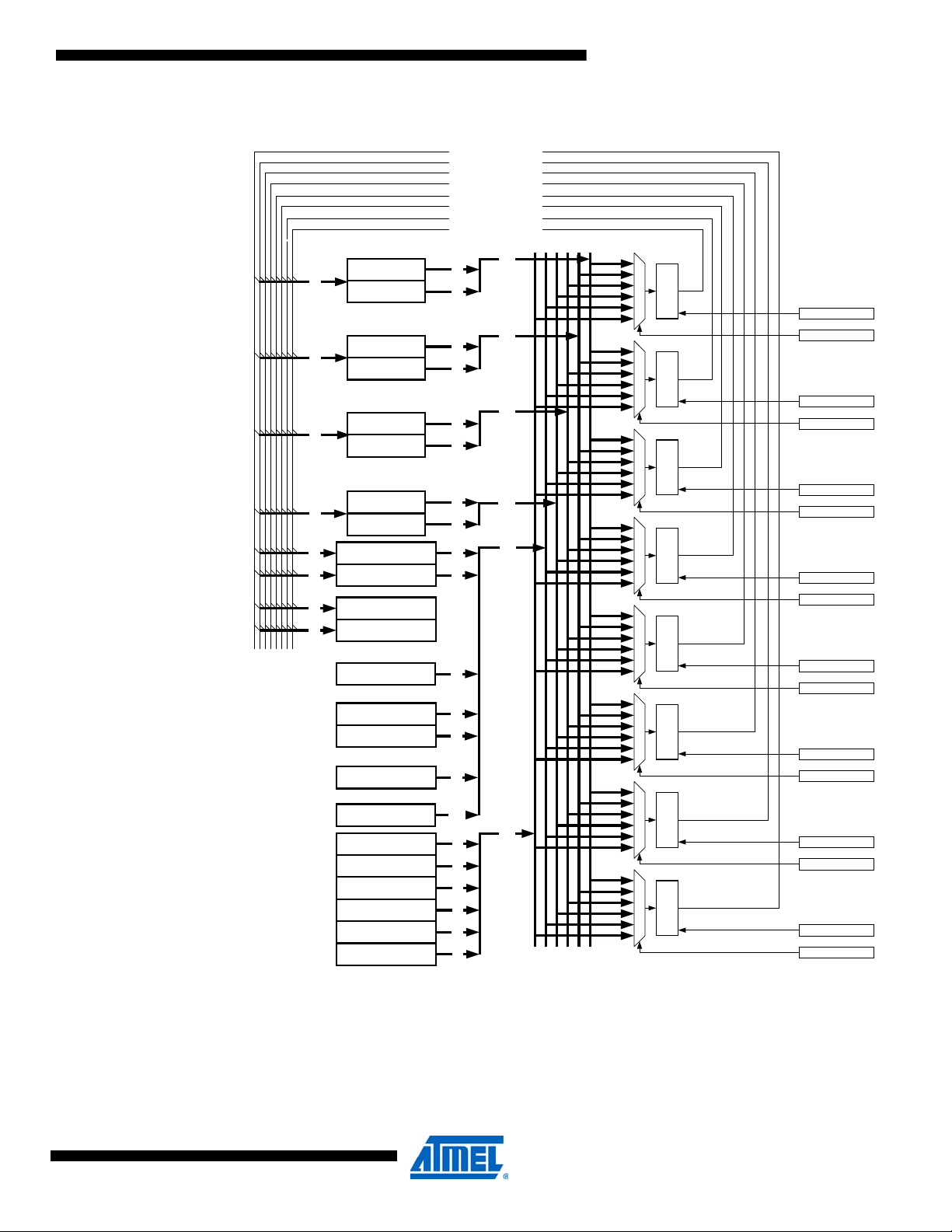
Figure 6-3. Event routing network.
Event Channel 7
Event Channel 6
Event Channel 5
Event Channel 4
Event Channel 3
Event Channel 2
Event Channel 1
Event Channel 0
(8)
(8)
TCC0
TCC1
TCD0
TCD1
(6)
(4)
(6)
(4)
(10)
(10)
Atmel AVR XMEGA AU
CH0CTRL[7:0]
CH0MUX[7:0]
(10)
(8)
(8)
(8)
(8)
(8)
(8)
TCE0
TCE1
TCF0
TCF1
ADCA
ADCB
DACA
DACB
USB
ACA
ACB
RTC
Clk
PER
PORTA
PORTB
PORTC
PORTD
PORTE
PORTF
(6)
(4)
(6)
(4)
(4)
(4)
(4)
(3)
(3)
(2)
(16)
(8)
(8)
(8)
(8)
(8)
(8)
(10)
(36)
(48)
CH1CTRL[7:0]
CH1MUX[7:0]
CH2CTRL[7:0]
CH2MUX[7:0]
CH3CTRL[7:0]
CH3MUX[7:0]
CH4CTRL[7:0]
CH4MUX[7:0]
CH5CTRL[7:0]
CH5MUX[7:0]
CH6CTRL[7:0]
CH6MUX[7:0]
CH7CTRL[7:0]
CH7MUX[7:0]
8331B–AVR–03/12
Eight multiplexers means that it is possible to route up to eight events at the same time. It is also
possible to route one event through several multiplexers.
Not all XMEGA devices contain all peripherals. This only means that a peripheral is not available
for generating or using events. The network configuration itself is compatible between all
devices.
75

6.5 Event Timing
An event normally lasts for one peripheral clock cycle, but some event sources, such as a low
level on an I/O pin, will generate events continuously. Details on this are described in the
datasheet for each peripheral, but unless otherwise stated, an event lasts for one peripheral
clock cycle.
It takes a maximum of two peripheral clock cycles from when an event is generated until the
event actions in other peripherals are triggered. This ensures short and 100% predictable
response times, independent of CPU or DMA controller load or software revisions.
6.6 Filtering
Each event channel includes a digital filter. When this is enabled, an event must be sampled
with the same value for a configurable number of system clock cycles before it is accepted. This
is primarily intended for pin change events.
6.7 Quadrature Decoder
The event system includes three quadrature decoders (QDECs), which enable the device to
decode quadrature input on I/O pins and send data events that a timer/counter can decode to
count up, count down, or index/reset. Table 6-2 on page 76 summarizes which quadrature
decoder data events are available, how they are decoded, and how they can be generated. The
QDECs and related features and control and status registers are available for event channels 0,
2, and 4.
Atmel AVR XMEGA AU
Table 6-2. Quadrature decoder data events.
STROBE DATA Data Event User Signaling Event User
0 0 No event No event
0 1 Index/reset No event
1 0 Count down Signaling event
1 1 Count up Signaling event
6.7.1 Quadrature Operation
A quadrature signal is characterized by having two square waves that are phase shifted 90
degrees relative to each other. Rotational movement can be measured by counting the edges of
the two waveforms. The phase relationship between the two square waves determines the
direction of rotation.
8331B–AVR–03/12
76

Atmel AVR XMEGA AU
00 10 11 01
QDPH0
QDPH90
QDINDX
Forward Direction
Backward
Direction
01 11 10 00
1 cycle / 4 states
QDPH0
QDPH90
QDINDX
Figure 6-4. Quadrature signals from a rotary encoder.
Figure 6-4 shows typical quadrature signals from a rotary encoder. The signals QDPH0 and
QDPH90 are the two quadrature signals. When QDPH90 leads QDPH0, the rotation is defined
as positive or forward. When QDPH0 leads QDPH90, the rotation is defined as negative or
reverse. The concatenation of the two phase signals is called the quadrature state or the phase
state.
6.7.2 QDEC Setup
8331B–AVR–03/12
In order to know the absolute rotary displacement, a third index signal (QINDX) can be used.
This gives an indication once per revolution.
For a full QDEC setup, the following is required:
• Thw or three I/O port pins for quadrature signal input
• Two event system channels for quadrature decoding
• One timer/counter for up, down, and optional index count
The following procedure should be used for QDEC setup:
1. Choose two successive pins on a port as QDEC phase inputs.
2. Set the pin direction for QDPH0 and QDPH90 as input.
3. Set the pin configuration for QDPH0 and QDPH90 to low level sense.
4. Select the QDPH0 pin as a multiplexer input for an event channel, n.
5. Enable quadrature decoding and digital filtering in the event channel.
6. Optional:
a. Set up a QDEC index (QINDX).
b. Select a third pin for QINDX input.
c. Set the pin direction for QINDX as input.
d. Set the pin configuration for QINDX to sense both edges.
e. Select QINDX as a multiplexer input for event channel n+1
f. Set the quadrature index enable bit in event channel n+1.
g. Select the index recognition mode for event channel n+1.
7. Set quadrature decoding as the event action for a timer/counter.
8. Select event channel n as the event source for the timer/counter.
77

• Set the period register of the timer/counter to ('line count' * 4 - 1), the line count of the
quadrature encoder.
• Enable the timer/counter without clock prescaling.
The angle of a quadrature encoder attached to QDPH0, QDPH90 (and QINDX) can now be read
directly from the timer/counter count register. If the count register is different from BOTTOM
when the index is recognized, the timer/counter error flag is set. Similarly, the error flag is set if
the position counter passes BOTTOM without the recognition of the index.
6.8 Register Description
6.8.1 CHnMUX – Event Channel n Multiplexer register
Bit 76543210
Read/Write R/W R/W R/W R/W R/W R/W R/W R/W
Initial Value 00000000
Atmel AVR XMEGA AU
CHnMUX[7:0] CHnMUX
• Bit 7:0 – CHnMUX[7:0]: Channel Multiplexer
These bits select the event source according to Table 6-3. This table is valid for all XMEGA
devices regardless of whether the peripheral is present or not. Selecting event sources from
peripherals that are not present will give the same result as when this register is zero. When this
register is zero, no events are routed through. Manually generated events will override CHnMUX
and be routed to the event channel even if this register is zero.
Table 6-3. CHnMUX[7:0] bit settings.
CHnMUX[7:4] CHnMUX[3:0] Group Configuration Event Source
0000 0000
0000 0001 (Reserved)
0000 0 0 1 X (Reserved)
0000 0 1 X X (Reserved)
0000 1000RTC_OVF RTC overflow
0000 1001RTC_CMP RTC compare match
0000 1010
0000 1 0 1 X (Reserved)
0000 1 1 X X (Reserved)
None (manually generated events
only)
USB start of frame on CH0
USB error on CH1
USB overflow on CH2
USB setup on CH3
(2)
(2)
(2)
(2)
8331B–AVR–03/12
0001 0000ACA_CH0 ACA channel 0
0001 0001ACA_CH1 ACA channel 1
0001 0010ACA_WIN ACA window
0001 0011ACB_CH0 ACB channel 0
78

Atmel AVR XMEGA AU
Table 6-3. CHnMUX[7:0] bit settings.
CHnMUX[7:4] CHnMUX[3:0] Group Configuration Event Source
0001 0100ACB_CH1 ACB channel 1
0001 0101ACB_WIN ACB window
0001 0 1 1 X (Reserved)
0001 1 X X X (Reserved)
0010 0 0 n ADCA_CHn ADCA channel n (n =0, 1, 2 or 3)
0010 0 1 n ADCB_CHn ADCB channel n (n=0, 1, 2 or 3)
0010 1 X X X (Reserved)
0011 XXXX (Reserved)
0100 XXXX (Reserved)
0101 0 n PORTA_PINn
0101 1 n PORTB_PINn
0110 0 n PORTC_PINn
0110 1 n PORTD_PINn
0111 0 n PORTE_PINn
0111 1 n PORTF_PINn
(1)
(1)
(1)
(1)
(1)
(1)
1000 M PRESCALER_M Clk
1001 XXXX (Reserved)
1010 XXXX (Reserved)
1011 XXXX (Reserved)
PORTA pin n (n= 0, 1, 2 ... or 7)
PORTB pin n (n= 0, 1, 2 ... or 7)
PORTC pin n (n= 0, 1, 2 ... or 7)
PORTD pin n (n= 0, 1, 2 ... or 7)
PORTE pin n (n= 0, 1, 2 ... or 7)
PORTF pin n (n= 0, 1, 2 ... or 7)
divide by 2M (M=0 to 15)
PER
1100 0 E See Table 6-4 Timer/counter C0 event type E
1100 1 E See Table 6-4 Timer/counter C1 event type E
1101 0 E See Table 6-4 Timer/counter D0 event type E
1101 1 E See Table 6-4 Timer/counter D1 event type E
1110 0 E See Table 6-4 Timer/counter E0 event type E
1110 1 E See Table 6-4 Timer/counter E1 event type E
1111 0 E See Table 6-4 Timer/counter F0 event type E
1111 1 E See Table 6-4 Timer/counter F1 event type E
Notes: 1. The description of how the ports generate events is described in ”Port Event” on page 150.
2. The different USB events can be selected for only event channel, 0 to 3.
Table 6-4. Timer/counter events.
T/C Event E Group Configuration Event Type
0 0 0 TCxn_OVF Over/Underflow (x = C, D, E or F) (n= 0 or 1)
0 0 1 TCxn_ERR Error (x = C, D, E or F) (n= 0 or 1)
0 1 X (Reserved)
1 0 0 TCxn_CCA Capture or compare A (x = C, D, E or F) (n= 0 or 1)
8331B–AVR–03/12
79

Table 6-4. Timer/counter events. (Continued)
T/C Event E Group Configuration Event Type
1 0 1 TCxn_CCB Capture or compare B (x = C, D, E or F) (n= 0 or 1)
1 1 0 TCxn_CCC Capture or compare C (x = C, D, E or F) (n= 0)
1 1 1 TCxn_CCD Capture or compare D (x = C, D, E or F) (n= 0)
6.8.2 CHnCTRL – Event Channel n Control register
Bit 7 6543210
– QDIRM[1:0] QDIEN QDEN DIGFILT[2:0] CHnCTRL
Read/Write R R/W R/W R/W R/W R/W R/W R
Initial Value00000000
• Bit 7 – Reserved
This bit is reserved and will always be read as zero. For compatibility with future devices, always
write this bit to zero when this register is written.
Atmel AVR XMEGA AU
• Bit 6:5 – QDIRM[1:0]: Quadrature Decode Index Recognition Mode
These bits determine the quadrature state for the QDPH0 and QDPH90 signals, where a valid
index signal is recognized and the counter index data event is given according to Table 6-5 on
page 80. These bits should only be set when a quadrature encoder with a connected index sig-
nal is used.These bits are available only for CH0CTRL, CH2CTRL, and CH4CTRL.
Table 6-5. QDIRM bit settings.
QDIRM[1:0] Index Recognition State
0 0 {QDPH0, QDPH90} = 0b00
0 1 {QDPH0, QDPH90} = 0b01
1 0 {QDPH0, QDPH90} = 0b10
1 1 {QDPH0, QDPH90} = 0b11
• Bit 4 – QDIEN: Quadrature Decode Index Enable
When this bit is set, the event channel will be used as a QDEC index source, and the index data
event will be enabled.
This bit is available only for CH0CTRL, CH2CTRL, and CH4CTRL.
• Bit 3 – QDEN: Quadrature Decode Enable
Setting this bit enables QDEC operation.
8331B–AVR–03/12
This bit is available only for CH0CTRL, CH2CTRL, and CH4CTRL.
• Bit 2:0 – DIGFILT[2:0]: Digital Filter Coefficient
These bits define the length of digital filtering used. Events will be passed through to the event
channel only when the event source has been active and sampled with the same level for the
number of peripheral clock cycles defined by DIGFILT.
80

Table 6-6. Digital filter coefficient values .
DIGFILT[2:0] Group Configuration Description
6.8.3 STROBE – Strobe register
If the STROBE register location is written, each event channel will be set according to the
STROBE[n] and corresponding DATA[n] bit settings, if any are unequal to zero.
A single event lasting for one peripheral clock cycle will be generated.
Atmel AVR XMEGA AU
000 1SAMPLE One sample
001 2SAMPLES Two samples
010 3SAMPLES Three samples
011 4SAMPLES Four samples
100 5SAMPLES Five samples
101 6SAMPLES Six samples
110 7SAMPLES Seven samples
111 8SAMPLES Eight samples
Bit 76543210
+0x10 STROBE[7:0] STROBE
Read/Write R/W R/W R/W R/W R/W R/W R/W R/W
Initial Value 00000000
6.8.4 DATA – Data register
This register contains the data value when manually generating a data event. This register must
be written before the STROBE register. For details, See ”STROBE – Strobe register” on page
81.
Bit 76543210
+0x11 DATA[7:0 ] DATA
Read/Write R/W R/W R/W R/W R/W R/W R/W R/W
Initial Value 00000000
8331B–AVR–03/12
81

6.9 Register Summary
Atmel AVR XMEGA AU
Address
+0x00 CH0MUX CH0MUX[7:0] 78
+0x01 CH1MUX CH1MUX[7:0] 78
+0x02 CH2MUX CH2MUX[7:0] 78
+0x03 CH3MUX CH3MUX[7:0] 78
+0x04 CH4MUX CH4MUX[7:0] 78
+0x05 CH5MUX CH5MUX[7:0] 78
+0x06 CH6MUX CH6MUX[7:0] 78
+0x07 CH7MUX CH7MUX[7:0] 78
+0x08 CH0CTRL – QDIRM[1:0] QDIEN QDEN DIGFILT[2:0] 80
+0x09 CH1CTRL – – – – – DIGFILT[2:0] 80
+0x0A CH2CTRL – QDIRM[1:0] QDIEN QDEN DIGFILT[2:0] 80
+0x0B CH3CTRL – – – – – DIGFILT[2:0] 80
+0x0C CH4CTRL – QDIRM[1:0] QDIEN QDEN DIGFILT[2:0] 80
+0x0D CH5CTRL – – – – – DIGFILT[2:0] 80
+0x0E CH6CTRL – – – – – DIGFILT[2:0] 80
+0x0F CH7CTRL – – – – – DIGFILT[2:0] 80
+0x10 STROBE STROBE[7:0] 81
+0x11 DATA DATA[7:0] 81
Name Bit 7 Bit 6 Bit 5 Bit 4 Bit 3 Bit 2 Bit 1 Bit 0 Page
8331B–AVR–03/12
82

7. System Clock and Clock Options
7.1 Features
• Fast start-up time
• Safe run-time clock switching
• Internal oscillators:
– 32MHz run-time calibrated oscillator
– 2MHz run-time calibrated oscillator
– 32.768kHz calibrated oscillator
– 32kHz ultra low power (ULP) oscillator with 1kHz output
• External clock options
– 0.4MHz - 16MHz crystal oscillator
– 32.768kHz crystal oscillator
– External clock
• PLL with 20MHz - 128MHz output frequency
– Internal and external clock options and 1x to 31x multiplication
– Lock detector
• Clock prescalers with 1x to 2048x division
• Fast peripheral clocks running at 2 and 4 times the CPU clock
• Automatic run-time calibration of internal oscillators
• External oscillator and PLL lock failure detection with optional non-maskable interrupt
Atmel AVR XMEGA AU
7.2 Overview
XMEGA devices have a flexible clock system supporting a large number of clock sources. It
incorporates both accurate internal oscillators and external crystal oscillator and resonator support. A high-frequency phase locked loop (PLL) and clock prescalers can be used to generate a
wide range of clock frequencies. A calibration feature (DFLL) is available, and can be used for
automatic run-time calibration of the internal oscillators to remove frequency drift over voltage
and temperature. An oscillator failure monitor can be enabled to issue a non-maskable interrupt
and switch to the internal oscillator if the external oscillator or PLL fails.
When a reset occurs, all clock sources except the 32kHz ultra low power oscillator are disabled.
After reset, the device will always start up running from the 2MHz internal oscillator. During normal operation, the system clock source and prescalers can be changed from software at any
time.
Figure 7-1 on page 84 presents the principal clock system in the XMEGA family of devices. Not
all of the clocks need to be active at a given time. The clocks for the CPU and peripherals can be
stopped using sleep modes and power reduction registers, as described in ”Power Management
and Sleep Modes” on page 105.
8331B–AVR–03/12
83

Figure 7-1. The clock system, clock sources, and clock distribution.
Real Time
Counter
Peripherals
RAM AVR CPU
Non-Volatile
Memory
Watchdog
Timer
Brown-out
Detector
System Clock Prescalers
USB
Prescaler
System Clock Multiplexer
(SCLKSEL)
PLLSRC
RTCSRC
DIV32
32 kHz
Int. ULP
32.768 kHz
Int. OSC
32.768 kHz
TOSC
2 MHz
Int. Osc
32 MHz
Int. Osc
0.4 – 16 MHz
XTAL
DIV32
DIV32
DIV4
XOSCSEL
PLL
USBSRC
TOSC1
TOSC2
XTAL1
XTAL2
clk
SYS
clk
RTC
clk
PER2
clk
PER
clk
CPU
clk
PER4
clk
USB
Atmel AVR XMEGA AU
8331B–AVR–03/12
84

7.3 Clock Distribution
Figure 7-1 on page 84 presents the principal clock distribution system used in XMEGA devices.
Atmel AVR XMEGA AU
7.3.1 System Clock - Clk
SYS
The system clock is the output from the main system clock selection. This is fed into the prescalers that are used to generate all internal clocks except the asynchronous and USB clocks.
7.3.2 CPU Clock - Clk
CPU
The CPU clock is routed to the CPU and nonvolatile memory. Halting the CPU clock inhibits the
CPU from executing instructions.
7.3.3 Peripheral Clock - Clk
PER
The majority of peripherals and system modules use the peripheral clock. This includes the DMA
controller, event system, interrupt controller, external bus interface and RAM. This clock is
always synchronous to the CPU clock, but may run even when the CPU clock is turned off.
7.3.4 Peripheral 2x/4x Clocks - Clk
Modules that can run at two or four times the CPU clock frequency can use the peripheral 2x
and peripheral 4x clocks.
7.3.5 Asynchronous Clock - Clk
RTC
The asynchronous clock allows the real-time counter (RTC) to be clocked directly from an external 32.768kHz crystal oscillator or the 32 times prescaled output from the internal 32.768kHz
oscillator or ULP oscillator. The dedicated clock domain allows operation of this peripheral even
when the device is in sleep mode and the rest of the clocks are stopped.
PER2
/Clk
PER4
7.3.6 USB Clock - Clk
USB
The USB device module requires a 12MHz or 48MHz clock. It has a separate clock source
selection in order to avoid system clock source limitations when USB is used.
7.4 Clock Sources
The clock sources are divided in two main groups: internal oscillators and external clock
sources. Most of the clock sources can be directly enabled and disabled from software, while
others are automatically enabled or disabled, depending on peripheral settings. After reset, the
device starts up running from the 2MHz internal oscillator. The other clock sources, DFLLs and
PLL, are turned off by default.
7.4.1 Internal Oscillators
The internal oscillators do not require any external components to run. For details on characteristics and accuracy of the internal oscillators, refer to the device datasheet.
7.4.1.1 32kHz Ultra Low Power Oscillator
This oscillator provides an approximate 32kHz clock. The 32kHz ultra low power (ULP) internal
oscillator is a very low power clock source, and it is not designed for high accuracy.The oscillator
employs a built-in prescaler that provides a 1kHz output. The oscillator is automatically
enabled/disabled when it is used as clock source for any part of the device. This oscillator can
be selected as the clock source for the RTC.
8331B–AVR–03/12
85

7.4.1.2 32.768kHz Calibrated Oscillator
This oscillator provides an approximate 32.768kHz clock. It is calibrated during production to
provide a default frequency close to its nominal frequency. The calibration register can also be
written from software for run-time calibration of the oscillator frequency. The oscillator employs a
built-in prescaler, which provides both a 32.768kHz output and a 1.024kHz output.
7.4.1.3 32MHz Run-time Calibrated Oscillator
The 32MHz run-time calibrated internal oscillator is a high-requency oscillator. It is calibrated
during production to provide a default frequency close to its nominal frequency. A digital frequency looked loop (DFLL) can be enabled for automatic run-time calibration of the oscillator to
compensate for temperature and voltage drift and optimize the oscillator accuracy. This oscillator can also be adjusted and calibrated to any frequency between 30MHz and 55MHz. The
production signature row contains 48 MHz calibration values intended used when the oscillator
is used a full-speed USB clock source.
7.4.1.4 2MHz Run-time Calibrated Oscillator
The 2MHz run-time calibrated internal oscillator is the default system clock source after reset. It
is calibrated during production to provide a default frequency close to its nominal frequency. A
DFLL can be enabled for automatic run-time calibration of the oscillator to compensate for temperature and voltage drift and optimize the oscillator accuracy.
Atmel AVR XMEGA AU
7.4.2 External Clock Sources
The XTAL1 and XTAL2 pins can be used to drive an external oscillator, either a quartz crystal or
a ceramic resonator. XTAL1 can be used as input for an external clock signal. The TOSC1 and
TOSC2 pins is dedicated to driving a 32.768kHz crystal oscillator.
7.4.2.1 0.4MHz - 16MHz Crystal Oscillator
This oscillator can operate in four different modes optimized for different frequency ranges, all
within 0.4MHz - 16MHz. Figure 7-2 shows a typical connection of a crystal oscillator or
resonator.
Figure 7-2. Crystal oscillator connection.
Two capacitors, C1 and C2, may be added to match the required load capacitance for the connected crystal.
C2
XTAL2
C1
XTAL1
GND
7.4.2.2 External Clock Input
To drive the device from an external clock source, XTAL1 must be driven as shown in Figure 7-
3 on page 87. In this mode, XTAL2 can be used as a general I/O pin.
8331B–AVR–03/12
86

Figure 7-3. External clock drive configuration.
General
Purpose
I/O
XTAL2
XTAL1
External
Clock
Signal
C1
C2
TOSC2
TOSC1
GND
7.4.2.3 32.768kHz Crystal Oscillator
A 32.768kHz crystal oscillator can be connected between the TOSC1 and TOSC2 pins and
enables a dedicated low frequency oscillator input circuit. A typical connection is shown in Fig-
ure 7-4 on page 87. A low power mode with reduced voltage swing on TOSC2 is available. This
oscillator can be used as a clock source for the system clock and RTC, and as the DFLL reference clock.
Figure 7-4. 32.768kHz crystal oscillator connection.
Atmel AVR XMEGA AU
Two capacitors, C1 and C2, may be added to match the required load capacitance for the connected crystal. For details on recommened TOSC characteristics and capacitor laod, refer to
device datasheets.
7.5 System Clock Selection and Prescalers
All the calibrated internal oscillators, the external clock sources (XOSC), and the PLL output can
be used as the system clock source. The system clock source is selectable from software, and
can be changed during normal operation. Built-in hardware protection prevents unsafe clock
switching. It is not possible to select a non-stable or disabled oscillator as the clock source, or to
disable the oscillator currently used as the system clock source. Each oscillator option has a status flag that can be read from software to check that the oscillator is ready.
The system clock is fed into a prescaler block that can divide the clock signal by a factor from 1
to 2048 before it is routed to the CPU and peripherals. The prescaler settings can be changed
from software during normal operation. The first stage, prescaler A, can divide by a factor of
from 1 to 512. Then, prescalers B and C can be individually configured to either pass the clock
through or combine divide it by a factor from 1 to 4. The prescaler guarantees that derived
clocks are always in phase, and that no glitches or intermediate frequencies occur when chang-
8331B–AVR–03/12
ing the prescaler setting. The prescaler settings are updated in accordance with the rising edge
of the slowest clock.
87

Figure 7-5. System clock selection and prescalers.
Prescaler A
1, 2, 4, ... , 512
Prescaler B
1, 2, 4
Prescaler C
1, 2
Internal 2MHz Osc.
Internal 32.768kHz Osc.
Internal 32MHz Osc.
External Oscillator or Clock.
Clk
CPU
Clock Selection
Clk
PER
Clk
SYS
Clk
PER2
Clk
PER4
Internal PLL.
f
OUTfIN
PLL_FAC⋅=
Atmel AVR XMEGA AU
Prescaler A divides the system clock, and the resulting clock is clk
be enabled to divide the clock speed further to enable peripheral modules to run at twice or four
times the CPU clock frequency. If Prescalers B and C are not used, all the clocks will run at the
same frequency as the output from Prescaler A.
The system clock selection and prescaler registers are protected by the configuration change
protection mechanism, employing a timed write procedure for changing the system clock and
prescaler settings. For details, refer to ”Configuration Change Protection” on page 13.
7.6 PLL with 1x-31x Multiplication Factor
The built-in phase locked loop (PLL) can be used to generate a high-frequency system clock.
The PLL has a user-selectable multiplication factor of from 1 to 31. The output frequency, f
given by the input frequency, f
Four different clock sources can be chosen as input to the PLL:
• 2MHz internal oscillator
• 32MHz internal oscillator divided by 4
• 0.4MHz - 16MHz crystal oscillator
• External clock
To enable the PLL, the following procedure must be followed:
. Prescalers B and C can
PER4
, multiplied by the multiplication factor, PLL_FAC.
IN
OUT
, is
8331B–AVR–03/12
1. Enable reference clock source.
2. Set the multiplication factor and select the clock reference for the PLL.
3. Wait until the clock reference source is stable.
4. Enable the PLL.
Hardware ensures that the PLL configuration cannot be changed when the PLL is in use. The
PLL must be disabled before a new configuration can be written.
It is not possible to use the PLL before the selected clock source is stable and the PLL has
locked.
The reference clock source cannot be disabled while the PLL is running.
88

7.7 DFLL 2MHz and DFLL 32MHz
Two built-in digital frequency locked loops (DFLLs) can be used to improve the accuracy of the
2MHz and 32MHz internal oscillators. The DFLL compares the oscillator frequency with a more
accurate reference clock to do automatic run-time calibration of the oscillator and compensate
for temperature and voltage drift. The choices for the reference clock sources are:
• 32.768kHz calibrated internal oscillator
• 32.768kHz crystal oscillator connected to the TOSC pins
• External clock
• USB start of frame
The DFLLs divide the oscillator reference clock by 32 to use a 1.024kHz reference. The reference clock is individually selected for each DFLL, as shown on Figure 7-6 on page 89.
Figure 7-6. DFLL reference clock selection.
Atmel AVR XMEGA AU
XOSCSEL
TOSC1
TOSC2
XTAL1
32.768 kHz Crystal Osc
External Clock
32.768 kHz Int. Osc
USB Start of Frame
DFLL32M
32 MHz Int. RCOSC
DFLL2M
2 MHz Int. RCOSC
clk
RC32MCREF
DIV32DIV32
clk
RC2MCREF
8331B–AVR–03/12
The ideal counter value representing the frequency ratio between the internal oscillator and a
1.024kHz reference clock is loaded into the DFLL oscillator compare register (COMP) during
reset. For the 32MHz oscillator, this register can be written from software to make the oscillator
run at a different frequency or when the ratio between the reference clock and the oscillator is
different (for example when the USB start of frame is used). The 48MHz calibration values must
be read from the production signature row and written to the 32MHz CAL register before the
DFLL is enabled with USB SOF as reference source.
89

Atmel AVR XMEGA AU
)(
RCnCREF
OSC
f
f
hexCOMP =
The value that should be written to the COMP register is given by the following formula:
When the DFLL is enabled, it controls the ratio between the reference clock frequency and the
oscillator frequency. If the internal oscillator runs too fast or too slow, the DFLL will decrement or
increment its calibration register value by one to adjust the oscillator frequency. The oscillator is
considered running too fast or too slow when the error is more than a half calibration step size.
Figure 7-7. Automatic run-time calibration.
clk
RCnCREF
t
DFLL CNT
COMP
RCnCREF
0
Frequency
The DFLL will stop when entering a sleep mode where the oscillators are stopped. After wake
up, the DFLL will continue with the calibration value found before entering sleep. The reset value
of the DFLL calibration register can be read from the production signature row.
When the DFLL is disabled, the DFLL calibration register can be written from software for manual run-time calibration of the oscillator.
7.8 PLL and External Clock Source Failure Monitor
A built-in failure monitor is available for the PLL and external clock source. If the failure monitor
is enabled for the PLL and/or the external clock source, and this clock source fails (the PLL
looses lock or the external clock source stops) while being used as the system clock, the device
will:
• Switch to run the system clock from the 2MHz internal oscillator
• Reset the oscillator control register and system clock selection register to their default values
• Set the failure detection interrupt flag for the failing clock source (PLL or external clock)
OK
RCOSC fast,
CALA decremented
RCOSC slow,
CALA incremented
8331B–AVR–03/12
90

Atmel AVR XMEGA AU
• Issue a non-maskable interrupt (NMI)
If the PLL or external clock source fails when not being used for the system clock, it is automatically disabled, and the system clock will continue to operate normally. No NMI is issued. The
failure monitor is meant for external clock sources above 32kHz. It cannot be used for slower
external clocks.
When the failure monitor is enabled, it will not be disabled until the next reset.
The failure monitor is stopped in all sleep modes where the PLL or external clock source are
stopped. During wake up from sleep, it is automatically restarted.
The PLL and external clock source failure monitor settings are protected by the configuration
change protection mechanism, employing a timed write procedure for changing the settings. For
details, refer to ”Configuration Change Protection” on page 13.
8331B–AVR–03/12
91

7.9 Register Description – Clock
7.9.1 CTRL – Control register
Bit 76543210
+0x00 – – – – –SCLKSEL[2:0]CTRL
Read/WriteRRRRRR/WR/WR/W
Initial Value00000000
• Bit 7:3 – Reserved
These bits are unused and reserved for future use. For compatibility with future devices, always
write these bits to zero when this register is written.
• Bit 2:0 – SCLKSEL[2:0]: System Clock Selection
These bits are used to select the source for the system clock. See Table 7-1 for the different
selections. Changing the system clock source will take two clock cycles on the old clock source
and two more clock cycles on the new clock source. These bits are protected by the configuration change protection mechanism. For details, refer to ”Configuration Change Protection” on
page 13.
Atmel AVR XMEGA AU
SCLKSEL cannot be changed if the new clock source is not stable. The old clock can not be disabled until the clock switching is completed.
Table 7-1. System clock selection.
SCLKSEL[2:0] Group Configuration Description
000 RC2MHZ 2MHz internal oscillator
001 RC32MHZ 32MHz internal oscillator
010 RC32KHZ 32.768kHz internal oscillator
011 XOSC External oscillator or clock
100 PLL Phase locked loop
101 — Reserved
110 — Reserved
111 — Reserved
7.9.2 PSCTRL – Prescaler register
This register is protected by the configuration change protection mechanism. For details, refer to
”Configuration Change Protection” on page 13.
Bit 76543210
+0x01 – PSADIV[4:0] PSBCDIV PSCTRL
Read/Write R R/W R/W R/W R/W R/W R/W R/W
Initial Value00000000
8331B–AVR–03/12
• Bit 7 – Reserved
This bit is unused and reserved for future use. For compatibility with future devices, always write
this bit to zero when this register is written.
92

Atmel AVR XMEGA AU
• Bit 6:2 – PSADIV[4:0]: Prescaler A Division Factor
These bits define the division ratio of the clock prescaler A according to Table 7-2. These bits
can be written at run-time to change the frequency of the Clk
clock, Clk
SYS
.
Table 7-2. Prescaler A division factor.
PSADIV[4:0] Group Configuration Description
00000 1 No division
00001 2 Divide by 2
00011 4 Divide by 4
00101 8 Divide by 8
00111 16 Divide by 16
01001 32 Divide by 32
01011 64 Divide by 64
01101 128 Divide by 128
01111 256 Divide by 256
10001 512 Divide by 512
10101 Reserved
10111 Reserved
clock relative to the system
PER4
11001 Reserved
11011 Reserved
11101 Reserved
11111 Reserved
• Bit 1:0 – PSBCDIV: Prescaler B and C Division Factors
These bits define the division ratio of the clock prescalers B and C according to Table 7-3. Prescaler B will set the clock frequency for the Clk
will set the clock frequency for the Clk
and Clk
PER
clock relative to the Clk
PER2
clocks relative to the Clk
CPU
clock. Prescaler C
PER4
clock. Refer
PER2
to Figure 7-5 on page 88 fore more details.
Table 7-3. Prescaler B and C division factors.
PSBCDIV[1:0] Group Configuration Prescaler B division Prescaler C division
00 1_1 No division No division
01 1_2 No division Divide by 2
10 4_1 Divide by 4 No division
11 2_2 Divide by 2 Divide by 2
8331B–AVR–03/12
93

7.9.3 LOCK – Lock register
Bit 76543210
+0x02 – – – – – – – LOCK LOCK
Read/WriteRRRRRRRR/W
Initial Value 0 0 0 0 0 0 0 0
• Bit 7:1 – Reserved
These bits are unused and reserved for future use. For compatibility with future devices, always
write these bits to zero when this register is written.
• Bit 0 – LOCK: Clock System Lock
When this bit is written to one, the CTRL and PSCTRL registers cannot be changed, and the
system clock selection and prescaler settings are protected against all further updates until after
the next reset. This bit is protected by the configuration change protection mechanism. For
details, refer to ”Configuration Change Protection” on page 13.
The LOCK bit can be cleared only by a reset.
Atmel AVR XMEGA AU
7.9.4 RTCCTRL – RTC Control register
Bit 76543210
+0x03 – – – – RTCSRC[2:0] RTCEN RTCCTRL
Read/WriteRRRRR/WR/WR/WR/W
Initial Value00000000
• Bit 7:4 – Reserved
These bits are unused and reserved for future use. For compatibility with future devices, always
write these bits to zero when this register is written.
• Bit 3:1 – RTCSRC[2:0]: RTC Clock Source
These bits select the clock source for the real-time counter according to Table 7-4.
Table 7-4. RTC clock source selection.
RTCSRC[2:0] Group Configuration Description
000 ULP 1kHz from 32kHz internal ULP oscillator
001 TOSC 1.024kHz from 32.768kHz crystal oscillator on TOSC
010 RCOSC 1.024kHz from 32.768kHz internal oscillator
011 — Reserved
8331B–AVR–03/12
100 — Reserved
101 TOSC32 32.768kHz from 32.768kHz crystal oscillator on TOSC
110 RCOSC32 32.768kHz from 32.768kHz internal oscillator
111 EXTCLK External clock from TOSC1
94
• Bit 0 – RTCEN: RTC Clock Source Enable
Setting the RTCEN bit enables the selected RTC clock source for the real-time counter.
7.9.5 USBSCTRL – USB Control register
Bit 76543210
+0x04
Read/Write R R R/W R/W R/W R/W R/W R/W
Initial Value00000000
– – USBPSDIV[2:0] USBSRC[1:0] USBSEN USBSCTRL
• Bit 7:6 – Reserved
These bits are unused and reserved for future use. For compatibility with future devices, always
write these bits to zero when this register is written.
• Bit 5:3 – USBPSDIV[2:0]: USB Prescaler Division Factor
These bits define the division ratio of the USB clock prescaler according to Table 7-5 on page
95. These bits are locked as long as the USB clock source is enabled.
Table 7-5. USB prescaler division factor.
Atmel AVR XMEGA AU
USBPSDIV[2:0] Group Configuration Description
000 1 No division
001 2 Divide by 2
010 4 Divide by 4
011 8 Divide by 8
100 16 Divide by 16
101 32 Divide by 32
110 — Reserved
111 — Reserved
• Bit 2:1 – USBSRC[1:0]: USB Clock Source
These bits select the clock source for the USB module according to Table 7-6 on page 95.
Table 7-6. USB clock source.
USBSRC[1:0] Group Configuration Description
00 PLL PLL
01 RC32M 32MHz internal oscillator
Note: 1. The 32MHz internal oscillator must be calibrated to 48MHz before selecting this as source for
the USB device module. Refer to ”DFLL 2MHz and DFLL 32MHz” on page 89.
(1)
8331B–AVR–03/12
• Bit 0 – USBSEN: USB Clock Source Enable
Setting this bit enables the selected clock source for the USB device module.
95

7.10 Register Description – Oscillator
7.10.1 CTRL – Oscillator Control register
Bit 76543210
+0x00 – – – PLLEN XOSCEN RC32KEN RC32MEN RC2MEN CTRL
Read/Write R R R R/W R/W R/W R/W R/W
Initial Value00000001
• Bit 7:5 – Reserved
These bits are unused and reserved for future use. For compatibility with future devices, always
write these bits to zero when this register is written.
• Bit 4 – PLLEN: PLL Enable
Setting this bit enables the PLL. Before the PLL is enabled, it must be configured with the
desired multiplication factor and clock source. See ”STATUS – Oscillator Status register” on
page 97.
• Bit 3 – XOSCEN: External Oscillator Enable
Setting this bit enables the selected external clock source. Refer to ”XOSCCTRL – XOSC Con-
trol register” on page 97 for details on how to select the external clock source. The external clock
source should be allowed time to stabilize before it is selected as the source for the system
clock. See ”STATUS – Oscillator Status register” on page 97.
Atmel AVR XMEGA AU
• Bit 2 – RC32KEN: 32.768kHz Internal Oscillator Enable
Setting this bit enables the 32.768kHz internal oscillator. The oscillator must be stable before it
is selected as the source for the system clock. See ”STATUS – Oscillator Status register” on
page 97.
• Bit 1 – RC32MEN: 32MHz Internal Oscillator Enable
Setting this bit will enable the 32MHz internal oscillator. The oscillator must be stable before it is
selected as the source for the system clock. See ”STATUS – Oscillator Status register” on page
97.
• Bit 0 – RC2MEN: 2MHz Internal Oscillator Enable
Setting this bit enables the 2MHz internal oscillator. The oscillator must be stable before it is
selected as the source for the system clock. See ”STATUS – Oscillator Status register” on page
97.
By default, the 2MHz internal oscillator is enabled and this bit is set.
8331B–AVR–03/12
96

7.10.2 STATUS – Oscillator Status register
Bit 765 4 3 2 1 0
+0x01 – – – PLLRDY XOSCRDY RC32KRDY RC32MRDY RC2MRDY STATUS
Read/Write R R R R R R R R
Initial Value 0 0 0 0 0 0 0 0
• Bit 7:5 – Reserved
These bits are unused and reserved for future use. For compatibility with future devices, always
write these bits to zero when this register is written.
• Bit 4 – PLLRDY: PLL Ready
This flag is set when the PLL has locked on the selected frequency and is ready to be used as
the system clock source.
• Bit 3 – XOSCRDY: External Clock Source Ready
This flag is set when the external clock source is stable and is ready to be used as the system
clock source.
• Bit 2 – RC32KRDY: 32.768kHz Internal Oscillator Ready
This flag is set when the 32.768kHz internal oscillator is stable and is ready to be used as the
system clock source.
Atmel AVR XMEGA AU
• Bit 1 – RC32MRDY: 32MHz Internal Oscillator Ready
This flag is set when the 32MHz internal oscillator is stable and is ready to be used as the system clock source.
• Bit 0 – RC2MRDY: 2MHz Internal Oscillator Ready
This flag is set when the 2MHz internal oscillator is stable and is ready to be used as the system
clock source.
7.10.3 XOSCCTRL – XOSC Control register
Bit 7 6 5 4 3210
+0x02 FRQRANGE[1:0] X32KLPM XOSCPWR XOSCSEL[3:0] XOSCCTRL
Read/Write R/W R/W R/W R/W R/W R/W R/W R/W
Initial Value 0 0 0 0 0 0 0 0
• Bit 7:6 – FRQRANGE[1:0]: 0.4 - 16MHz Crystal Oscillator Frequency Range Select
These bits select the frequency range for the connected crystal oscillator according to Table 7-7
on page 98.
8331B–AVR–03/12
97

Atmel AVR XMEGA AU
Table 7-7. 16MHz crystal oscillator frequency range selection.
Typical Frequency
FRQRANGE[1:0] Group Configuration
00 04TO2 0.4MHz - 2MHz 100-300
01 2TO9 2MHz - 9MHz 10-40
10 9TO12 9MHz - 12MHz 10-40
11 12TO16 12MHz - 16MHz 10-30
Note: Refer to Electrical characteristics section in device datasheet to retrieve the best setting for a
given frequency.
Range
Recommended Range for
Capacitors C1 and C2 (pF)
• Bit 5 – X32KLPM: Crystal Oscillator 32.768kHz Low Power Mode
Setting this bit enables the low power mode for the 32.768kHz crystal oscillator. This will reduce
the swing on the TOSC2 pin.
• Bit 4 – XOSCPWR: Crystal Oscillator Drive
Setting this bit will increase the current in the 0.4MHz - 16MHz crystal oscillator and increase the
swing on the XTAL2 pin. This allows for driving crystals with higher load or higher frequency
than specfiied by the FRQRANGE bits.
• Bit 3:0 – XOSCSEL[3:0]: Crystal Oscillator Selection
These bits select the type and start-up time for the crystal or resonator that is connected to the
XTAL or TOSC pins. See Table 7-8 for crystal selections. If an external clock or external oscillator is selected as the source for the system clock, see ”CTRL – Oscillator Control register” on
page 96. This configuration cannot be changed.
Table 7-8. External oscillator selection and start-up time.
XOSCSEL[3:0] Group Configuration Selected Clock Source Start-up Time
0000 EXTCLK
0010 32KHZ
0011 XTAL_256CLK
0111 XTAL_1KCLK
1011 XTAL_16KCLK 0.4MHz - 16MHz XTAL 16K CLK
Notes: 1. This option should be used only when frequency stability at startup is not important for the
application. The option is not suitable for crystals.
2. This option is intended for use with ceramic resonators. It can also be used when the frequency stability at startup is not important for the application.
3. When the external oscillator is used as the reference for a DFLL, only EXTCLK and 32KHZ
can be selected.
(3)
(3)
(1)
(2)
External Clock 6 CLK
32.768kHz TOSC 16K CLK
0.4MHz - 16MHz XTAL 256 CLK
0.4MHz - 16MHz XTAL 1K CLK
8331B–AVR–03/12
98

7.10.4 XOSCFAIL – XOSC Failure Detection register
Bit 765432 1 0
+0x03 – – – – PLLFDIF PLLFDEN XOSCFDIF XOSCFDEN XOSCFAIL
Read/Write R R R R R/W R/W R/W R/W
Initial Value000000 0 0
• Bit 7:4 – Reserved
These bits are unused and reserved for future use. For compatibility with future devices, always
write these bits to zero when this register is written.
• Bit 3 – PLLFDIF: PLL Fault Detection Flag
If PLL failure detection is enabled, PLLFDIF is set when the PLL looses lock. Writing logic one to
this location will clear PLLFDIF.
• Bit 2 – PLLFDEN: PLL Fault Detection Enable
Setting this bit will enable PLL failure detection. A non-maskable interrupt will be issued when
PLLFDIF is set.
Atmel AVR XMEGA AU
This bit is protected by the configuration change protection mechanism. Refer to ”Configuration
Change Protection” on page 13 for details.
• Bit 1 – XOSCFDIF: Failure Detection Interrupt Flag
If the external clock source oscillator failure monitor is enabled, XOSCFDIF is set when a failure
is detected. Writing logic one to this location will clear XOSCFDIF.
• Bit 0 – XOSCFDEN: Failure Detection Enable
Setting this bit will enable the failure detection monitor, and a non-maskable interrupt will be
issued when XOSCFDIF is set.
This bit is protected by the configuration change protection mechanism. Refer to ”Configuration
Change Protection” on page 13 for details. Once enabled, failure detection can only be disabled
by a reset.
7.10.5 RC32KCAL – 32kHz Oscillator Calibration register
Bit 76543210
+0x04 RC32KCAL[7:0] RC32KCAL
Read/Write R/W R/W R/W R/W R/W R/W R/W R/W
Initial Valuexxxxxxxx
8331B–AVR–03/12
• Bit 7:0 – RC32KCAL[7:0]: 32.768kHz Internal Oscillator Calibration Register
This register is used to calibrate the 32.768kHz internal oscillator. A factory-calibrated value is
loaded from the signature row of the device and written to this register during reset, giving an
oscillator frequency close to 32.768kHz. The register can also be written from software to calibrate the oscillator frequency during normal operation.
99

7.10.6 PLLCTRL – PLL Control register
Bit 76543210
+0x05 PLLSRC[1:0] PLLDIV PLLFAC[4:0] PLLCTRL
Read/Write R/W R/W R/W R/W R/W R/W R/W R/W
Initial Value00000000
• Bit 7:6 – PLLSRC[1:0]: Clock Source
The PLLSRC bits select the input source for the PLL according to Table 7-9 on page 100.
Table 7-9. PLL Clock Source
PLLSRC[1:0] Group Configuration PLL Input Source
00 RC2M 2MHz internal oscillator
01 — Reserved
10 RC32M 32MHz internal oscillator
11 XOSC External clock source
Notes: 1. The 32.768kHz TOSC cannot be selected as the source for the PLL. An external clock must be
a minimum 0.4MHz to be used as the source clock.
Atmel AVR XMEGA AU
(1)
• Bit 5 – PLLDIV: PLL Divided Output Enable
Setting this bit will divide the output from the PLL by 2.
• Bit 4:0 – PLLFAC[4:0]: Multiplication Factor
These bits select the multiplication factor for the PLL. The multiplication factor can be in the
range of from 1x to 31x.
7.10.7 DFLLCTRL – DFLL Control register
Bit 765432 1 0
+0x06 – – – – – RC32MCREF[1:0] RC2MCREF DFLLCTRL
Read/Write R R R R R R/W R/W R/W
Initial Value 0 0 0 0 0 0 0 0
• Bit 7:3 – Reserved
These bits are unused and reserved for future use. For compatibility with future devices, always
write these bits to zero when this register is written.
• Bit 2:1 – RC32MCREF[1:0]: 32MHz Oscillator Calibration Reference
These bits are used to select the calibration source for the 32MHz DFLL according to the Table
7-10 on page 101. These bits will select only which calibration source to use for the DFLL. In
addition, the actual clock source that is selected must enabled and configured for the calibration
to function.
8331B–AVR–03/12
100
 Loading...