

Page 1

Features
• Utilizes the AVR
• AVR - High-performance and Low-power RISC Architecture
– 118 Powerful Instructions - Most Single Clock Cycle Execution
– 32 x 8 General Purpose Working Registers
– Up to 8 MIPS Throughput at 8 MHz
• Data and Nonvolatile Program Memory
– 2K Bytes of In-System Programmable Flash
Endurance 1,000 Write/Erase Cycles
– 128 Bytes of internal SRAM
– 128 Bytes of In-System Programmab le EEPR OM
Endurance: 100,000 Write/Erase Cycles
– Programming Lock for Flash Program and EEPROM Data Security
• Peripheral Features
– One 8-bit Timer/Counter with Separate Prescaler
– Programmable Watchdog Timer with On-chip Oscillator
– SPI Serial Interface for In-System Programming
• Special Microcontroller Features
– Low-power Idle and Power Down Modes
– External and Internal Interrupt Sources
– Power-on Reset Circu it
– Selectable On-chip RC Oscillator
• Specifications
– Low-power, High-speed CMOS Process Technology
– Fully Static Operation
• Power Consumption at 4 MHz, 3V, 25°C
– Active: 2.4 mA
– Idle Mode: 0.5 mA
– Power Down Mode: <1 µA
• I/O and Packages
– 5 Programmable I/O Lines
– 8-pin PDIP and SOIC
• Operating Voltages
– 2.7 - 6.0V (ATtiny22L)
– 4.0 - 6.0V (ATtiny22)
• Speed Grades
– 0 - 4 MHz (ATtiny22L)
– 0 - 8 MHz (ATtiny22)
®
RISC Architecture
8-bit
Microcontr oller
with 2K Bytes of
In-System
Programmable
Flash
A Ttiny22
A Ttiny22L
Preliminary
Description
The ATtiny22/ L is a low-p ower CMO S 8 -bit micr ocon troll ers b ase d on the AV R RIS C
architecture. By executing powerful instructions in a single clock cycle, the ATtiny22/L
achieves throughputs approaching 1 MIPS per MHz allowing the system designer to
optimize power consumption versus processing speed.
Pin Configuration
PDIP/SOIC
8
RESET
(CLOCK) PB3
PB4
GND
1
2
3
4
VCC
7
PB2 (SCK/T0)
6
PB1 (MISO/INT0)
5
PB0 (MOSI)
Rev. 1273A–04/99
1
Page 2
The AVR core combines a rich instruction set with 32 general purpose working registers. All the 32 registers are directly
connected to the Arithm etic Lo gic Unit (A LU), al lowing two ind ependen t regist ers to b e access ed in on e single inst ruction
executed in one clock cycle. The resulting architecture is more code efficient while achieving throughputs up to ten times
faster than conventional CISC microcontrollers.
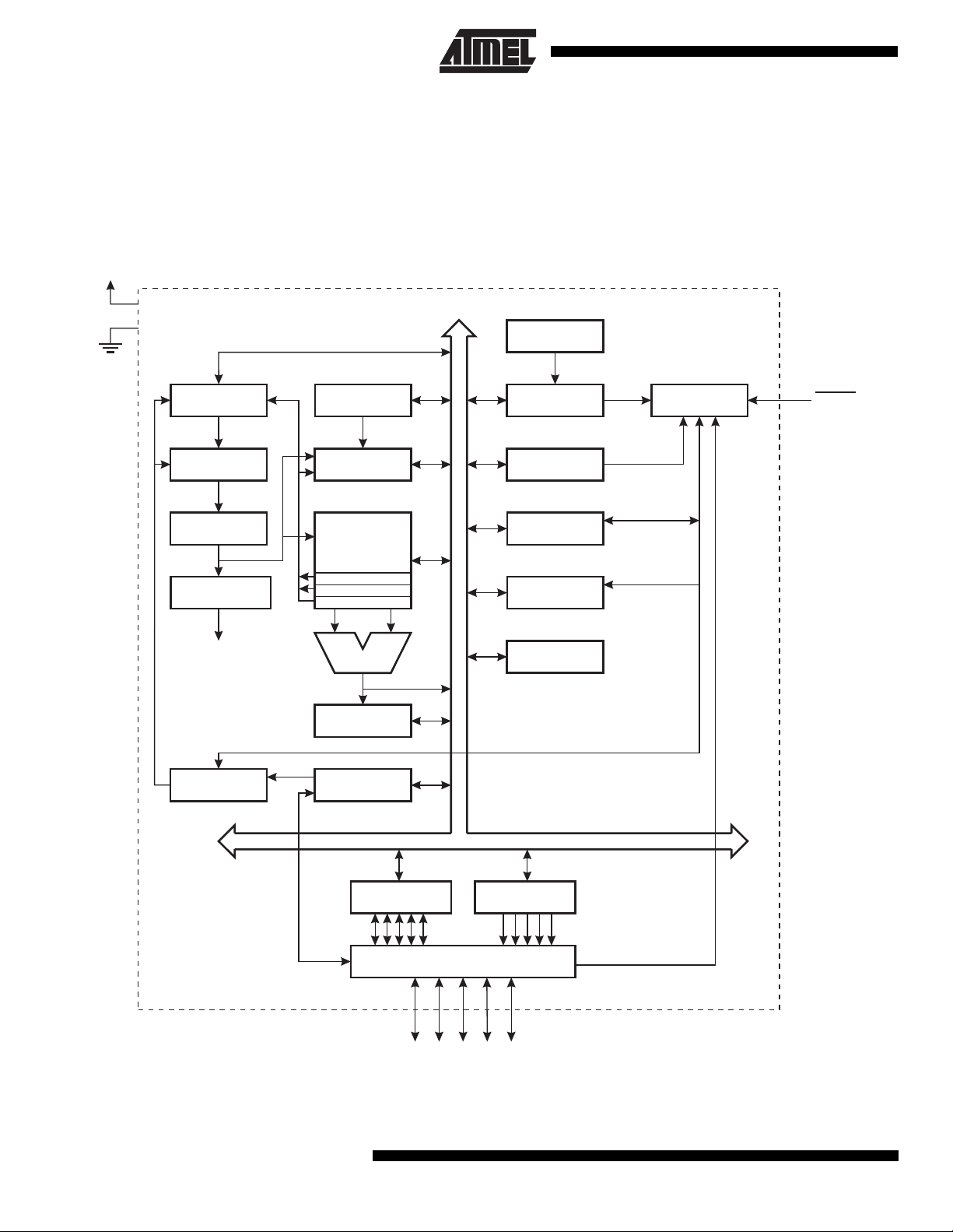
Block Diagram
Figure 1. The ATtiny22/L Block Diagram
VCC
8-BIT DATA BUS
INTERNAL
OSCILLATOR
GND
PROGRAM
COUNTER
PROGRAM
FLASH
INSTRUCTION
REGISTER
INSTRUCTION
DECODER
CONTROL
LINES
PROGRAMMING
LOGIC
STACK
POINTER
SRAM
GENERAL
PURPOSE
REGISTERS
X
Y
Z
ALU
STATUS
REGISTER
SPI
WATCHDOG
TIMER
MCU CONTROL
REGISTER
TIMER/
COUNTER
INTERRUPT
UNIT
EEPROM
TIMING AND
CONTROL
RESET
DATA REGISTER
PORTB
PORTB DRIVERS
PB0 - PB4
2
ATtiny22/22L
DATA DIR.
REG. PORTB
Page 3

ATtiny22/22L
The ATtiny22/L provides the following features: 2K bytes of In-System Programmable Flash, 128 bytes EEPROM,
128 bytes SRAM, five gen er al purpo se I/O l ine s, 32 g ene ral p ur pos e w or king r e gist ers , an 8- bit ti mer /counter, internal and
external interrupts , progr ammab le Wa tchdog Timer with i nternal osci llator, an S PI se rial p ort fo r Flash Memory downl oading and two softwa re selectable powe r saving modes. T he Idle Mode st ops the CPU while a llowing the SRAM,
timer/counters, SPI port and interrupt system to continue functioning. The power down mode saves the register contents
but freezes the oscillator, disabling all other chip functions until the next interrupt or hardware reset.
The device is manufactured using Atmel’s high density nonvolatile memory technology. The on-chip Flash allows the
program memory to be reprogrammed in-system through an SPI serial interface. By combining an 8-bit RISC CPU with ISP
Flash on a monolithic chip, the Atmel ATtiny22/L is a powerful microcontroller that provides a highly flexible and cost effective solution to many embedded control applications.
The ATtiny22/L AVR is supported with a full suite of program and system development tools including: C compilers, macro
assemblers, program debugger/simulators, in-circuit emulators, and evaluation kits.
Pin Descriptions ATtiny22/L
VCC
Supply voltage pin.
GND
Ground pin.
Port B (PB4..PB0)
Port B is a 5-bi t bi-dir ectional I /O port . Port pi ns can pr ovide in ternal p ull-up res istors (s elected fo r each bit). Wh en the
device is clocked from an external clock source, PB3 is used as the clock input. The port B pins are tri-stated when a reset
condition becomes active, even if the clock is not running.
RESET
Reset input. An exter na l res et is g ene ra ted by a l ow le vel o n th e RE SE T pin. Res et pulses lon ger than 50 ns will generate
a reset, even if the clock is not running. Shorter pulses are not guaranteed to generate a reset.
CLOCK
Clock signal input in external clock mode.
Clock Options
External Clock
The ATtiny22/L can be clocked by an ext ernal cl ock sign al, as s hown in Figur e 2, or by the on -chip RC os cill ator. This RC
oscillator runs at a nomi nal frequ ency of 1 MHz (VCC = 5V). A fuse bit - RCEN - in the Fla sh memory selects the on -chip
RC oscillator as the clock source when programmed (“0”). The ATtiny22/L is shipped with this bit programmed.
3
Page 4
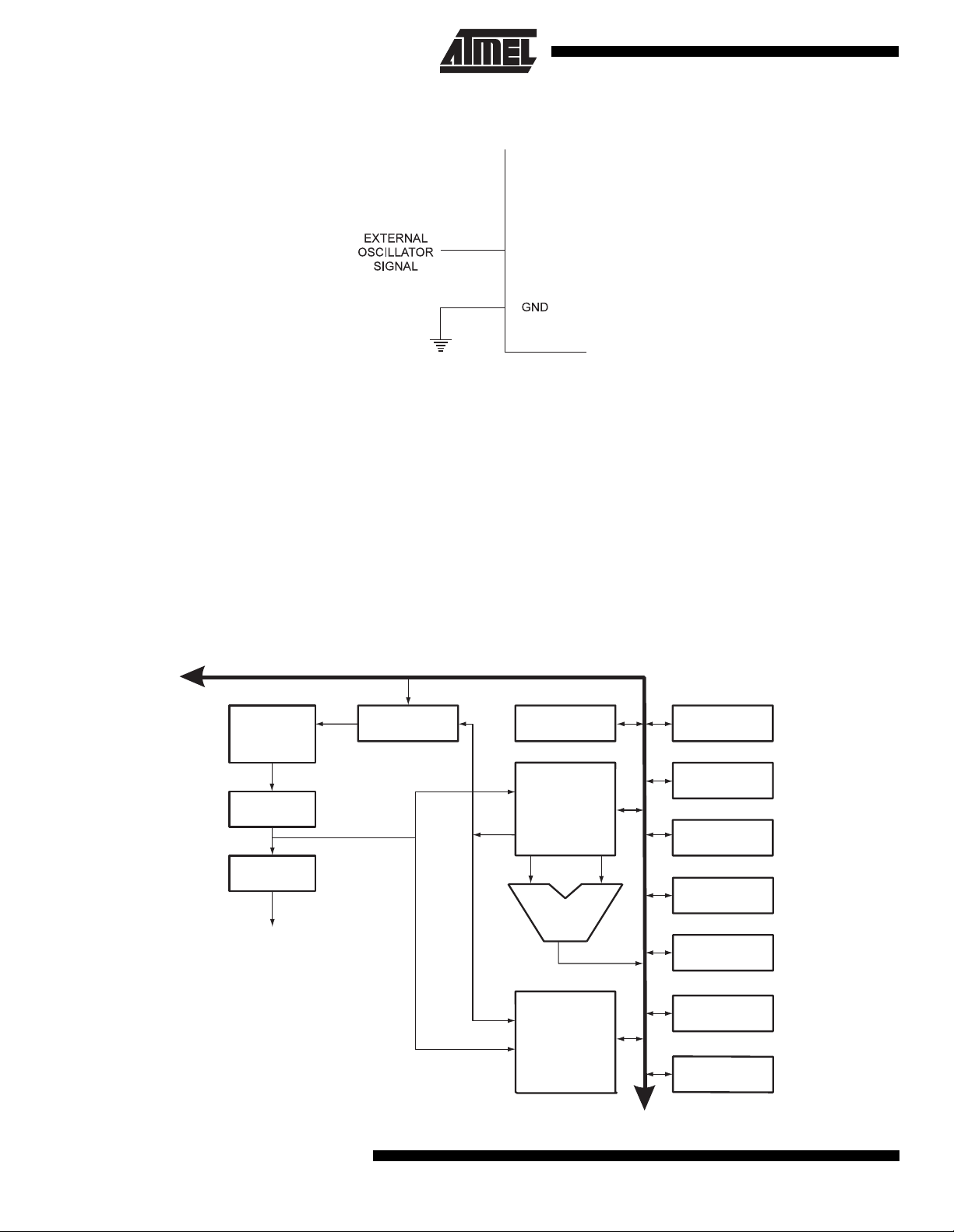
Figure 2. External Clock Drive Configuration
PB3
Architectural Overview
The fast-access register file concept contains 32 x 8-bit general purpose working registers with a single clock cycle access
time. This means that during one single clock cycle, one arithmetic logic unit (ALU) operation is executed. Two operands
are output from the registe r file, the operati on is executed, and the result is sto red back in the regi ster file in one cl ock
cycle.
Six of the 32 registers can be used as three 16-bit indirect address register pointers for Data Space addressing enabling
efficient address cal cula tions . One of th e thre e addres s poi nters i s also u sed as the a ddress pointer for the c onstan t table
look up function. These added function registers are the 16-bit X-register, Y-register and Z-register.
Figure 3. The ATtiny22/L AVR RISC Architecture
AVR
1K x 16
Program
Flash
Instruction
Register
Instruction
Decoder
Control Lines
Program
Counter
ATtiny22/L Architecture
Data Bus 8-bit
Status
and Test
32 x 8
General
Purpose
Registers
ALU
Direct Addressing
Indirect Addressing
128 x 8
Data
SRAM
Control
Registers
Interrupt
Unit
SPI
Unit
8-bit
Timer/Counter
Watchdog
Timer
I/O Lines
128 x 8
EEPROM
4
ATtiny22/22L
Page 5
ATtiny22/22L
The ALU supports arithmetic and logic functions between registers or between a constant and a register. Single register
operations are also executed in the ALU. Figure 3 shows the ATtiny22/L AVR RISC microcontroller architecture.
In addition to the register operation, the conventional memory addressing modes can be used on the register file as well.
This is enabled by the fact that the regi ster file is ass igned the 32 lowe rmost Data Sp ace addresse s ($00 - $1F), allowing
them to be accessed as though they were ordinary memory locations.
The I/O memory space contains 64 addresses for CPU peripheral functions as Control Registers, Timer/Counters,
A/D-converters, and oth er I/O func tions. The I/O memory can be ac cesse d directl y, or as th e Data Spa ce locati ons follo wing those of the register file, $20 - $5F.
The AVR has Harvard architecture - wi th separate memories a nd buses for pro gram and data. The p rogram memory is
accessed with a two stage pipeline. While one instruction is bei ng executed, the next instructio n is pre-fetched from the
program memory. This concept enables instructions to be executed in every clock cycle. The program memory is in-system
downloadable Flash memory.
With the relative jump and call instructions, the whole 1K address space is directly accessed. Most AVR instructions have a
single 16-bit word format. Every program memory address contains a 16- or 32-bit instruction.
During interrupts and subrouti ne calls, the return addres s program counter (PC) is sto red on the stack. The stack is
effectively allocated in the general da ta S RAM , a nd c onsequently the sta ck s iz e i s onl y li mi ted by the total SRAM size and
the usage of the SRAM. All user programs must initialize the SP in the reset routine (before subroutines or interrupts are
executed). The 8-bit stack pointer SP is read/write accessible in the I/O space.
The 128 bytes data SRAM + regist er file and I/O register s can be easily a ccessed thro ugh the five different ad dressing
modes supported in the AVR architecture.
The memory spaces in the AVR architecture are all linear and regular memory maps.
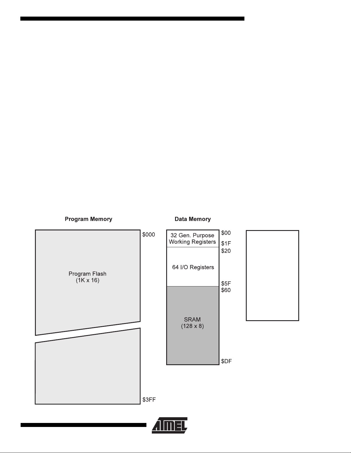
Figure 4. Memory Maps
EEPROM Data Memory
$000
EEPROM
(128 x 8)
$07F
5
Page 6

A flexible interrupt module has its control registers in the I/O space with an additional global interrupt enable bit in the status
register. All the different interrupts have a separate interrupt vector in the interrupt vector table at the beginning of the
program memory. T he different in terrupts ha ve priority in accordan ce with thei r interrupt ve ctor positi on. The lower the
interrupt vector address, the higher the priority.
General Purpose Register File
Figure 5 shows the structure of the 32 general purpose registers in the CPU.
Figure 5. AVR CPU General Purpose Working Registers
7 0 Addr.
R0 $00
R1 $01
R2 $02
…
R13 $0D
General R14 $0E
Purpose R15 $0F
Working R16 $10
Registers R17 $11
…
R26 $1A X-register low byte
R27 $1B X-register high byte
R28 $1C Y-register low byte
R29 $1D Y-register high byte
R30 $1E Z-register low byte
R31 $1F Z-register high byte
All the register oper ating instruc tions in th e instruc tion set ha ve direc t and single c ycle acces s to all registers. The only
exception is the five constant arithmetic and logic instructions SBCI, SUBI, CPI, ANDI, ORI between a constant and a
register and the LDI instructi on for load immediate con stant data. These instructi ons apply to the second hal f of the registers in the register file - R16..R31. The general SBC, SUB, CP, AND, OR and all other operations between two registers or
on a single register apply to the entire register file.
As shown in Fig ure 5, e ach reg ister is al so a ssigned a da ta mem ory add ress , map ping t hem di rectly into the fir st 32 locations of the user Data Space. Although the register file is not physically implemented as SRAM locations, this memory
organization provides great flexibility in access of the registers, as the X, Y and Z registers can be set to index any register
in the file.
6
ATtiny22/22L
Page 7

ATtiny22/22L
X-Register, Y-Register, and Z-Register
The registers R26..R31 have some added functions to their general purpose usage. These registers are the address pointers for indirect addressing of the Data Space. The three indirect address registers X, Y and Z are defined as:
Figure 6. The X, Y, and Z Registers
15 0
X - register 7 0 7 0
R27 ($1B) R26 ($1A)
15 0
Y - register 7 0 7 0
R29 ($1D) R28 ($1C)
15 0
Z - register 7 0 7 0
R31 ($1F) R30 ($1E)
In the different addr essing modes these add ress reg isters have func tions as fix ed di splacem ent, au tomatic inc rement and
decrement (see the descriptions for the different instructions).
ALU - Arithmetic Logic Unit
The high-performa nce AV R ALU oper ates in di rect conn ectio n with all the 32 gener al purpos e working registe rs. Withi n a
single clock cy c le, ALU operations between regis ter s in th e r eg is ter fi le ar e exec uted . The A LU o per ati on s a re di v ided i nto
three main categories - arithmetic, logic and bit-functions
In-System Programmable Flash Program Memory
The ATtiny22/L contains 2K b ytes on- chip In- System Prog rammabl e Flash memor y for p rogram s torage. Sinc e all instruc tions are 16- or 32- bit words, the Flash is organiz ed as 1 K x 16. The Flash m emory has an enduranc e of at l east 1000
write/erase cycles.
The ATtiny22/L Program Counter PC is 10 bits wide, hence addressing the 1024 program memory addresses. See
page 38 for a detailed description on Flash data programming.
Constant tables must be allocated within the address 0-2K (see the LPM - Load Program Memory instruction description).
See page 9 for the different addressing modes.
EEPROM Data Memory
The ATtiny22/L contains 128 bytes of EEPROM data memory. It is organized as a separate data space, in which single
bytes can be read and written. The EEPROM has an endurance of at least 100,000 write/erase cycles. The access
between the EEPROM and the CPU is described on page 30 specifying the EEPROM address register, the EEPROM data
register, and the EEPROM control register.
For the SPI data downloading, see page 38 for a detailed description.
7
Page 8
SRAM Data Memory
The following figure shows how the ATtiny22/L Data Memory is organized:
Figure 7. SRAM Organization
Register File Data Address Space
R0 $00
R1 $01
R2 $02
……
R29 $1D
R30 $1E
R31 $1F
I/O Registers
$00 $20
$01 $21
$02 $22
……
$3D $5D
$3E $5E
$3F $5F
Internal SRAM
$60
$61
$62
…
$DD
$DE
$DF
The 224 Data Memory loca tions address the Regi ster file, I/O M emo ry and the data SRA M. The fi rst 96 loc ation s addres s
the Register File + I/O Memory, and the next 128 locations address the data SRAM.
The five different addressing modes for the data memory cover: Direct, Indirect with Displacement, Indirect, Indirect with
Pre-Decrement and Indirect with Post-Increment. In the register file, registers R26 to R31 feature the indirect addressing
pointer registers.
The Direct addressing reaches the entire data address space.
The Indirect with Displ acement mo de features 63 addres s locations reach from the base address gi ven by the Y and Z
register.
When using register indirect addressing modes with automatic pre-decrement and post-increment, the address registers X,
Y and Z are used and decremented and incremented.
The 32 general purpose working registers, 64 I/O registers and the 128 bytes of data SRAM in the ATtiny22/L are all
directly accessible through all these addressing modes.
8
ATtiny22/22L
Page 9
ATtiny22/22L
Program and Data Addressing Modes
The ATtiny22/L AVR RISC Microcon troller supports powerful and efficient addr essing modes for access to the program
memory (Flash) and dat a memor y. This s ection de scr ibes the d iffere nt addres sing modes su pporte d by th e AVR a rchitecture. In the figures, OP means the operation code part of the instruction word. To simplify, not all figures show the exact
location of the addressing bits.
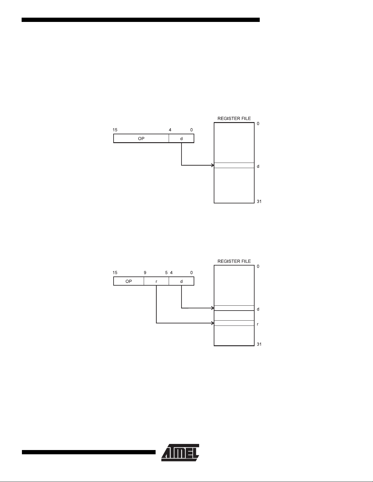
Register Direct, Single Register Rd
Figure 8. Direct Single Register Addressing
The operand is contained in register d (Rd).
Register Direct, Two Registers Rd and Rr
Figure 9. Direct Register Addressing, Two Registers
Operands are contained in register r (Rr) and d (Rd). The result is stored in register d (Rd).
9
Page 10
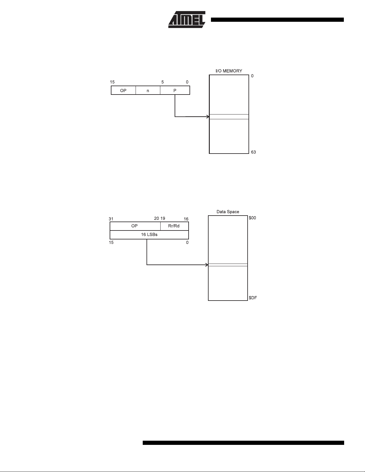
I/O Direct
Figure 10. I/O Direct Addressing
Operand address is contained in 6 bits of the instruction word. n is the destination or source register address.
Data Direct
Figure 11. Direct Data Addressing
A 16-bit Data Address is contained in the 16 LSBs of a two-word instr uction. Rd/Rr specify the de stination or source
register.
10
ATtiny22/22L
Page 11
ATtiny22/22L
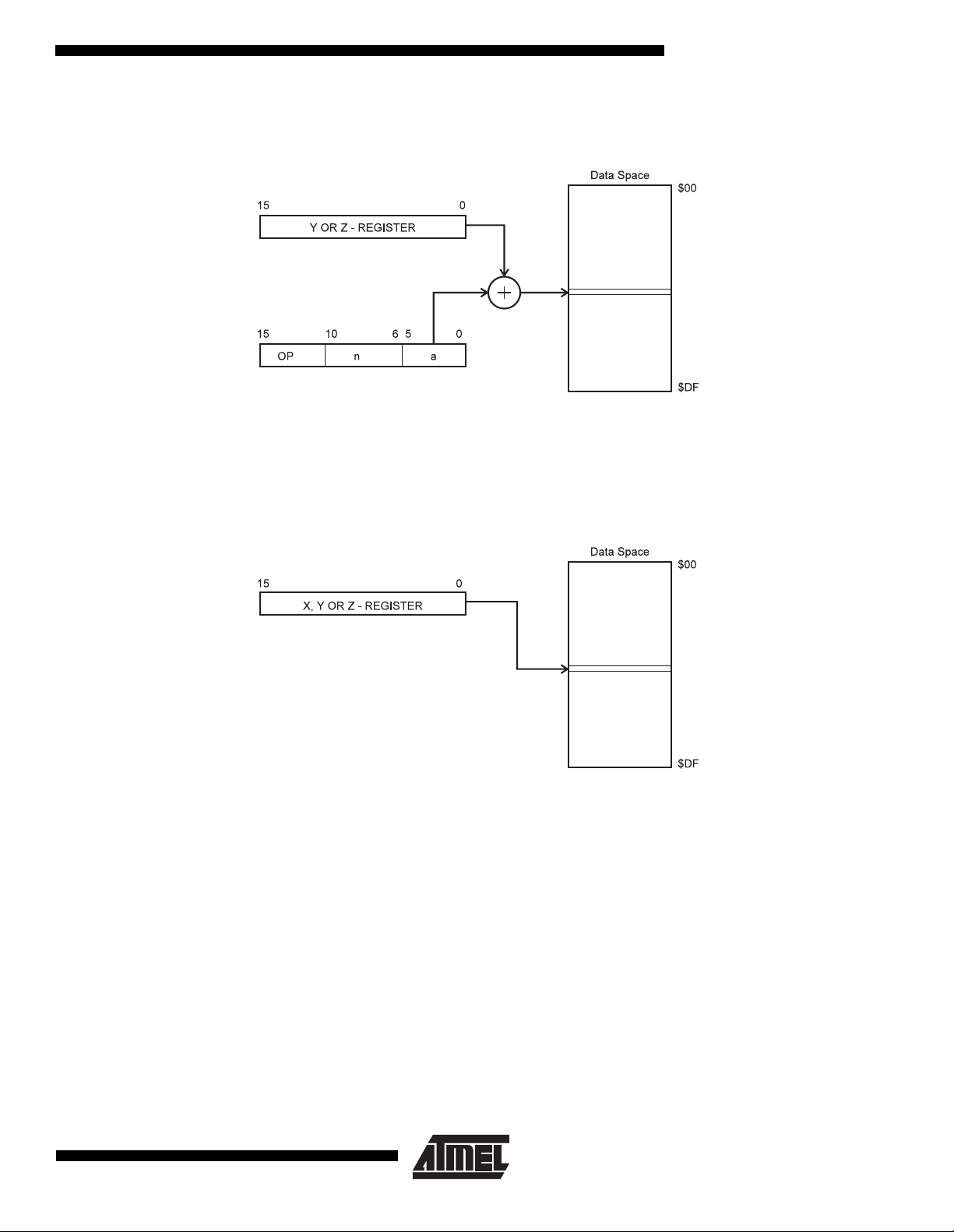
Data Indirect with Displacement Figure 12. Data Indirect with Displacement
Operand address is the result o f the Y or Z- register contents ad ded to the addre ss contained in 6 bits of the instruction
word.
Data Indirect
Figure 13. Data Indirect Addressing
Operand address is the contents of the X, Y or the Z-register.
11
Page 12

Data Indirect With Pre-Decrement
Figure 14. Data Indirect Addressing With Pre-Decrement
The X, Y or the Z-register is decremen ted be fore the oper ation. Operand ad dress is the decrem ented co ntents of the X, Y
or the Z-register.
Data Indirect With Post-Increment
Figure 15. Data Indirect Addressing With Post-Increment
The X, Y or the Z-register is incremented after the operation. Operand address is the content of the X, Y or the Z-register
prior to incrementing.
12
ATtiny22/22L
Page 13
ATtiny22/22L
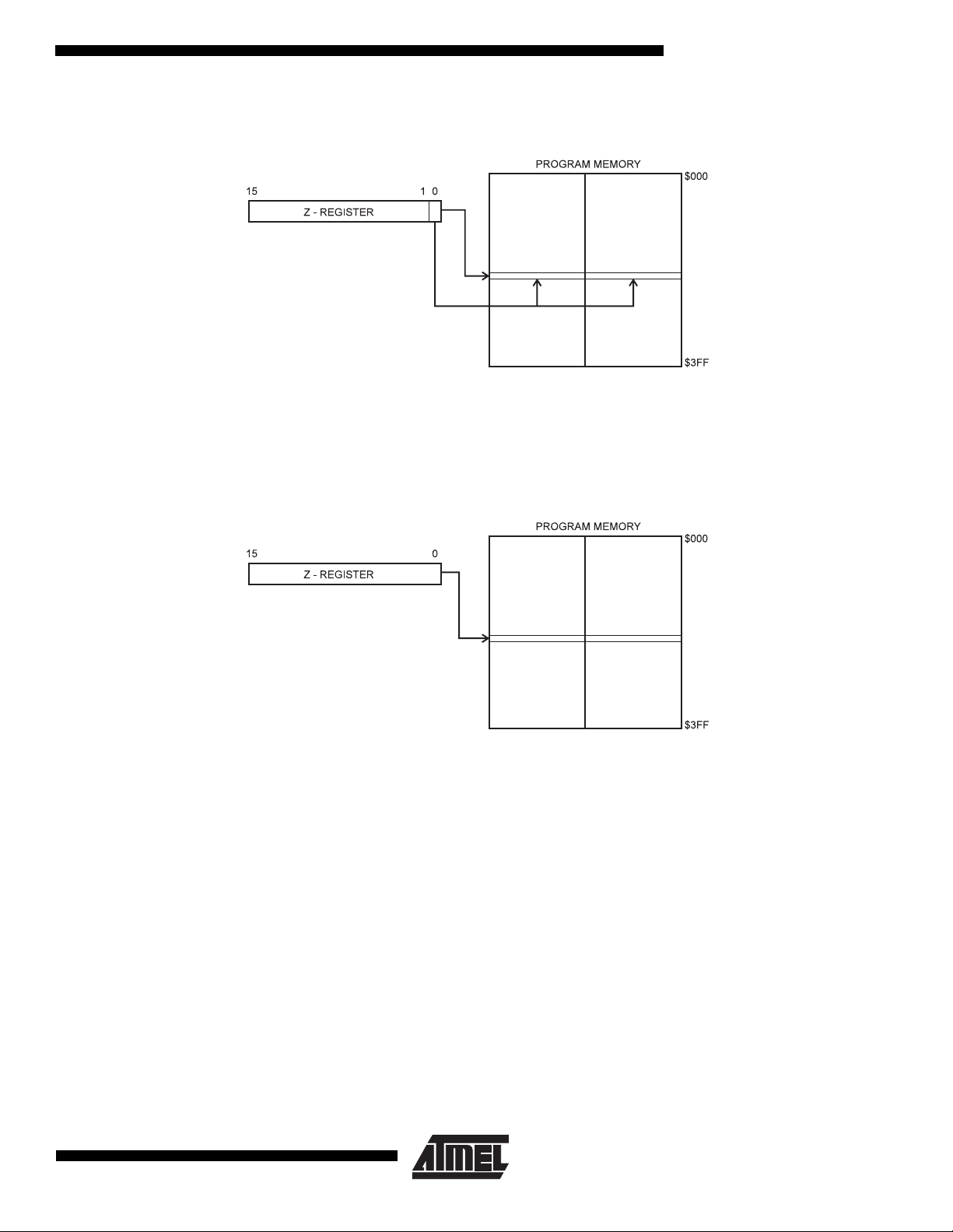
Constant Addressing Using the LPM Instruction
Figure 16. Code Memory Constant Addressing
Constant byte address i s sp ec ified by th e Z- regi st er c onte nts. The 15 MSBs select wor d add ress (0 - 1K ) , th e LSB s elec ts
low byte if cleared (LSB = 0) or high byte if set (LSB = 1).
Indirect Program Addressing, IJMP and ICALL
Figure 17. Indirect Program Memory Addressing
Program execution continues at address contained by the Z-register (i.e., the PC is loaded with the content of the
Z-register).
13
Page 14
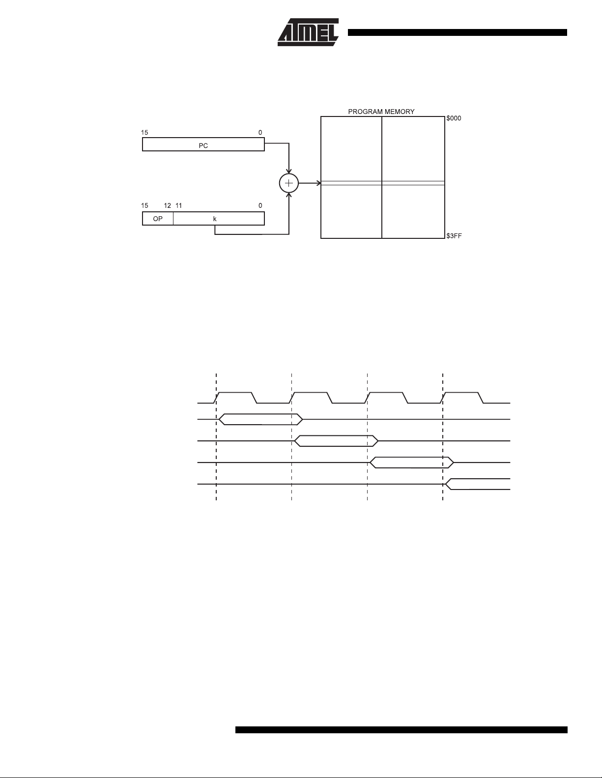
Relative Program Addressing, RJMP and RCALL
Figure 18. Relative Program Memory Addressing
Program execution continues at address PC + k + 1. The relative address k is -2048 to 2047.
Memory Access and Instruction Execution Timing
This section describes the general access timing concepts for instruction execution and internal memory access.
The AVR CPU is driven by the System Clock Ø, directly generated from the external clock signal applied to the CLOCK pin.
No internal clock division is used.
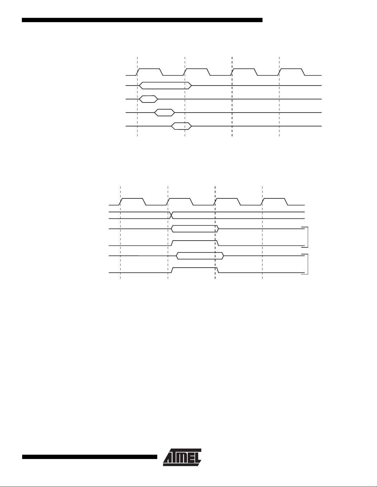
Figure 19. The Parallel Instruction Fetches and Instruction Executions
T1 T2 T3 T4
System Clock Ø
1st Instruction Fetch
1st Instruction Execute
2nd Instruction Fetch
2nd Instruction Execute
3rd Instruction Fetch
3rd Instruction Execute
4th Instruction Fetch
Figure 19 shows the parallel instruction fetches and instruction executions enabled by the Harvard architecture and the
fast-access register file concept. This is the basic pipelining concept to obtain up to 1 MIPS per MHz with the corresponding
unique results for functions per cost, functions per clocks, and functions per power-unit.
14
ATtiny22/22L
Page 15
ATtiny22/22L
Figure 20. Single Cycle ALU Operation
T1 T2 T3 T4
System Clock Ø
Total Execution Time
Register Operands Fetch
ALU Operation Execute
Result Write Back
Figure 20 shows the internal tim ing con ce pt for the re gis ter fil e. In a si ngle cl oc k cy cle an ALU oper at ion using two r egi ste r
operands is executed, and the result is stored back to the destination register.
Figure 21. On-Chip Data SRAM Access Cycles
T1 T2 T3 T4
System Clock Ø
Address
Data
WR
Data
RD
Prev. Address
Address
The internal data SRAM access is performed in two System Clock cycles as described in Figure 21.
Read Write
15
Page 16

I/O Memory
The I/O space definition of the ATtiny22/L is shown in the following table:
Table 1. ATtiny22/L I/O Space
Address Hex Name Function
$3F ($5F) SREG Status REGister
$3D ($5D) SPL Stack Pointer Low
$3B ($5B) GIMSK General Interrupt MaSK register
$3A ($5A) GIFR General Interrupt Flag Register
$39 ($59) TIMSK Timer/Counter Interrupt MaSK register
$38 ($58) TIFR Timer/Counter Interrupt Flag register
$35 ($55) MCUCR MCU Control Register
$34 ($54) MCUSR MCU Status Register
$33 ($53) TCCR0 Timer/Counter 0 Control Register
$32 ($52) TCNT0 Timer/Counter 0 (8-bit)
$21 ($41) WDTCR Watchdog Timer Control Register
$1E ($3E) EEAR EEPROM Address Register
$1D ($3D) EEDR EEPROM Data Register
$1C ($3C) EECR EEPROM Control Register
$18 ($38) PORTB Data Register, Port B
$17 ($37) DDRB Data Direction Register, Port B
$16 ($36) PINB Input Pins, Port B
Note: Reserved and unused locations are not shown in the table.
All the different ATtiny22/L I/O and peripherals are placed in the I/O space. The different I/O locations are accessed by the
IN and OUT instructio ns transferring data between the 32 ge neral purpose working register s and the I/O space. I/O
registers withi n the add ress ra nge $00 - $1F a re direc tly bit -accessi ble usi ng the S BI and C BI ins tructio ns. In t hese
registers, the value of single bits can be checked by using the SBIS and SBIC instructions. Refer to the instruction set
chapter for more details. When using the I/O specific commands IN, OUT the I/O addresses $00 - $3F must be used. When
addressing I/O registers as SRAM, $20 must be added to this address. All I/O register addresses throughout this document
are shown with the SRAM address in parentheses.
For compatibility with fu tur e dev ices , r eser v ed bi ts sh oul d be writte n to z er o if accessed. Reserved I/O m emo ry a ddr ess es
should never be written.
Some of the status flags are cleared by writing a logical one to them. Note that the CBI and SBI instructions will operate on
all bits in the I/O reg ister, wr iting a o ne back int o any f lag r ead as set, th us clea ring the flag. The CBI and SBI i nstruc tion s
work with registers $00 to $1F only.
The different I/O and peripherals control registers are explained in the following sections.
Status Register - SREG
The AVR status register - SREG - at I/O space location $3F ($5F) is defined as:
Bit 76543210
$3F ($5F) I T H S V N Z C SREG
Read/Write R/W R/W R/W R/W R/W R/W R/W R/W
Initial value 0 0 0 0 0 0 0 0
16
ATtiny22/22L
Page 17

ATtiny22/22L
• Bit 7 - I: Global Interrupt Enable
The global interrup t ena ble b it mu st b e se t (on e) for the interr upts to be enab led. The i ndivi dual interru pt enable contr ol i s
then performed in sep arate contr ol regis ters. If the glo bal interr upt enabl e register is cleared ( zero), non e of the interr upts
are enabled inde pendent of the indi vidua l interrup t enable setting s. The I-bi t is clear ed by hard ware aft er an inter rupt has
occurred, and is set by the RETI instruction to enable subsequent interrupts.
Bit 6 - T: Bit Copy Storage
•
The bit copy instructions BLD (Bit LoaD) and BST (Bit STore) use the T bit as source and destination for the operated bit. A
bit from a register in the regi s ter fil e c an be cop ie d in to T by the B ST in st ructi on, and a bit in T can be copied into a bit in a
register in the register file by the BLD instruction.
Bit 5 - H: Half Carry Flag
•
The half carry flag H indicates a half carry in some arithmetic operations. See the Instruction Set Description for detailed
information.
Bit 4 - S: Sign Bit, S = N ⊕ V
•
The S-bit is always an exclusive or between the negative flag N and the two’s complement overflow flag V. See the Instruc-
tion Set Description for detailed information.
Bit 3 - V: Two’s Complement Overflow Flag
•
The two’s complement overflow flag V supports two’s complement arithmetics. See the Instruction Set Description for
detailed information.
Bit 2 - N: Negative Flag
•
The negative flag N indicates a negative result from an arithmetical or logical operation. See the Instruction Set Description
for detailed information.
Bit 1 - Z: Zero Flag
•
The zero flag Z indicates a zero result from an arithmetical or logical operation. See the Instruction Set Description for
detailed information.
Bit 0 - C: Carry Flag
•
The carry flag C indicates a carry in an arithmetical or logical operation. See the Instruction S et Description for detailed
information.
Note that the status register is not automatically stored when entering an interrupt routine and restored when returning from
an interrupt routine. This must be handled by software.
Stack Pointer - SPL
An 8-bit register at I/O address $3 D ($5D) forms th e stack poin ter of the ATtin y22/L. 8 bits are us ed to address the
128 bytes of SRAM in locations $60 - $DF.
Bit 76543210
$3D ($5D) SP7 SP6 SP5 SP4 SP3 SP2 SP1 SP0 SPL
Read/Write R/W R/W R/W R/W R/W R/W R/W R/W
Initial value 0 0 0 0 0 0 0 0
The Stack Pointer points to the data SRA M stack area where the Su broutin e and Interru pt Stacks are lo cated. Thi s Stack
space in the data SRAM must be de fined by the program bef ore any subroutine calls are executed or interr upts are
enabled. The stack pointer must be set to point above $60. The Stack Pointer is decremented by one when data is pushed
onto the Stack with the PUSH instruction, and it is decremented by two when an address is pushed onto the Stack with
subroutine calls and interrupts. The Stack Pointer is incremented by one when data is popped from the Stack with the POP
instruction, and it is incremented b y two when an address is popped from the Stack with return fro m subroutine RET or
return from interrupt RETI.
17
Page 18

Reset and Interrupt Handling
The ATtiny22/L provides two interrupt sources. These interrupts and the separate reset vector, each have a separate
program vector in the progr am me mor y s pac e. Bo th int er rupts ar e assi gn ed individual enable bit s whic h mus t be se t ( one )
together with the I-bit in the status register in order to enable the interrupt.
The lowest addresses in the program memor y space are automatical ly defined as the Reset and Interrupt vector s. The
complete list of ve ctors is shown i n Table 2 . The li st also determines th e prior ity levels of the in terrupts . The lower the
address the higher is the priority level. RESET has the highest priority, next is INT0 - the External Interrupt Request 0, etc.
Table 2. Reset and Inte rru pt Vectors
Vector No. Program Address Source Interrupt Definition
1 $000 RESET Hardware Pin, Power-on Reset and Watchdog Reset
2 $001 INT0 External Interrupt Request 0
3 $002 TIMER0, OVF0 Timer/Counter0 Overflow
The most typical program setup for the Reset and Interrupt Vector Addresses are:
Address Labels Code Comments
$000 rjmp RESET ; Reset Handler
$001 rjmp EXT_INT0 ; IRQ0 Handler
$002 rjmp TIM_OVF0 ; Timer0 Overflow Handler;
$003 MAIN: ldi r16, low(RAMEND) ; Main program start
out SPL, r16
<instr> xxx
… … … …
Reset Sources
The ATtiny22/L provides three sources of reset:
• Power-On Reset. The MCU is reset when the supply voltage is below the power-on reset threshold (V
• External Reset. The MCU is reset when a low level is present on the RESET
pin for more than 50 ns.
POT
).
• Watchdog Reset. The MCU is reset when the Watchdog timer period expires and the Watchdog is enabled.
During reset, all I/O registers are set to their initial values, and the program starts execution from address $000. The
instruction placed in addre ss $000 must be an RJMP - relative j ump - instructio n to the reset handli ng routine. If the
program never enables an inte r rupt s ou rce, the interrupt vecto rs a re no t us ed , an d reg ular program code can be p la ced at
these locations. The circuit diagram in Figure 22 shows the reset logic. Table 3 defines the timing and electrical parameters
of the reset circuitry.
18
ATtiny22/22L
Page 19

Figure 22. Reset Logic
ATtiny22/22L
VCC
RESET
Power-On Reset
Circuit
100 - 500K
Reset Circuit
Watchdog
Timer
On-Chip
RC-Oscillator
POR
14-Stage Ripple Counter
Q0 Q13Q3
COUNTER RESET
QS
R
Q
INTERNAL
RESET
The ATtiny22/L has a fixed startup time.
Table 3. Reset Characteristics (V
Symbol Parameter Min Typ Max Units
(1)
V
POT
V
RST
t
TOUT
Notes: 1. The Power-On Reset will not work unless the supply voltage has been below V
Power-On Reset Threshold Voltage, rising 1.0 1.4 1.8 V
Power-On Reset Threshold Voltage, falling 0.4 0.6 0.8 V
RESET Pin Threshold Voltage 0.6 V
Reset Delay Time-Out Period ATtiny22/L 11 16 21 µs
= 5.0V)
CC
CC
(falling).
POT
V
Table 4. Reset Characteristics (VCC = 3.0V)
Symbol Parameter Min Typ Max Units
(1)
V
POT
V
RST
t
TOUT
Notes: 1. The Power-On Reset will not work unless the supply voltage has been below V
Power-On Reset Threshold Voltage, rising 1.0 1.4 1.8 V
Power-On Reset Threshold Voltage, falling 0 .4 0.6 0.8 V
RESET Pin Threshold Voltage 0. 6 V
CC
Reset Delay Time-Out Period ATtiny22/L 22 32 42 µs
(falling).
POT
V
Power-On Reset
The ATtiny22/L is designed for use in systems where it can operate from the internal RC oscillator or in applications where
a clock signal is prov id ed by an ex terna l c lo ck s ourc e. A fter V
has reached V
CC
, the device will start after the tim e t
POT
TOUT
(see Figure 23). If the clock sign al is provide d by an external clock so urce, the cloc k must not be applied un til VCC has
reached the minimum voltage defined for the applied frequency.
The start-up time t
is one watchdog cycl e. The frequ ency o f the w atchdog os cill ator is vol tage dep endent a s show n in
TOUT
“Typical character is tics ” on page 44.
19
Page 20
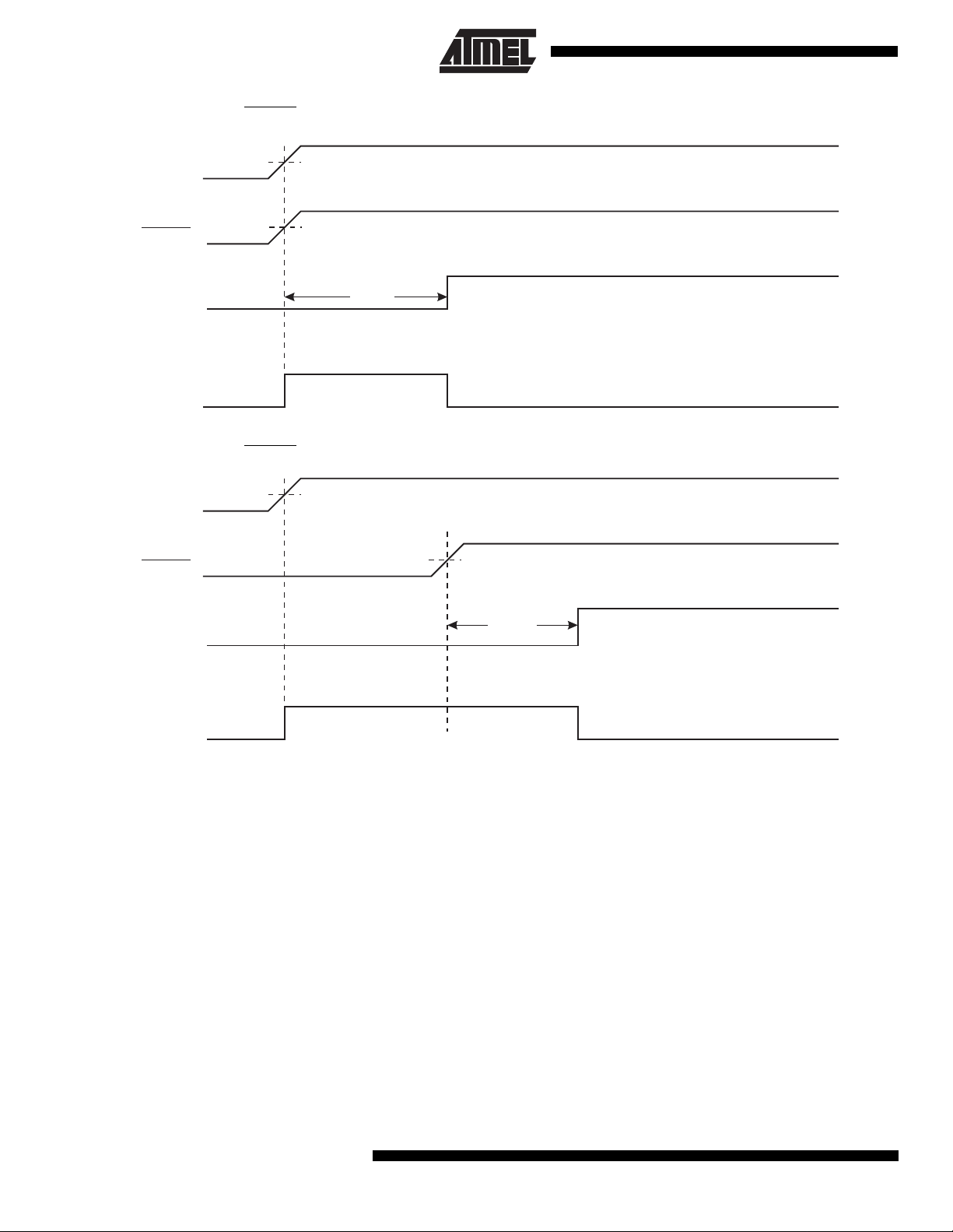
Figure 23. MCU Start-Up, RESET Tied to VCC.
V
V
POT
RST
t
TOUT
VCC
RESET
TIME-OUT
INTERNAL
RESET
Figure 24. MCU Start-Up, RESET
VCC
RESET
TIME-OUT
INTERNAL
RESET
Controlled Externally
V
POT
V
RST
t
TOUT
20
ATtiny22/22L
Page 21

ATtiny22/22L
External Reset
An external reset is generated by a low level on the RESET
if the clock is n ot runnin g. Shorter pulses a re not gu aranteed t o generate a rese t. When the applied signal r eaches the
Reset Threshold Voltage - V
- on its positive edge, the delay timer starts the MCU after the Time-out period t
RST
expired.
Figure 25. External Reset During Operation
pin. Reset pulses longer than 50 ns will generate a reset, even
has
TOUT
Watchdog Reset
When the Watchdog times out, it will generate a short reset pulse of 1 XTAL cycle duration. On the falling edge of this
pulse, the delay timer starts counting the Time-out period t
. Refer to page 28 for details on operation of the Watchdog.
TOUT
Figure 26. Watchdog Reset During Operation
21
Page 22

MCU Status Register - MCUSR
The MCU Status Register provides information on which reset source caused a MCU reset:
Bit 76543210
$34 ($54)------EXTRFPORFMCUSR
Read/WriteRRRRRRR/WR/W
Initial value 0 0 0 0 0 0 See bit description
Bit 7..2 - Res: Reserved Bits
•
These bits are reserved bits in the ATtiny22/L and always read as zero.
Bit 1 - EXTRF: External Reset Flag
•
After a power-on reset, this bit is undefined (X). It will be set by an external reset. A watchdog reset will leave this bit
unchanged.
Bit 0 - PORF: Power-On Reset Flag
•
This bit is set by a power-on reset. A watchdog reset or an external reset will leave this bit unchanged.
To summarize, the following table shows the value of these two bits after the three modes of reset.
Table 5. PORF and EXTRF Values after Reset
Reset Source PORF EXTRF
Power-On Reset 1 undefined
External Reset unchanged 1
Watchdog Reset unchanged unchanged
To make use of these bits to identify a reset condition, the user software should clear both the PORF and EXTRF bits as
early as possible in the program. Checking the PORF and EXTRF values is done before the bits are cleared. If the bit is
cleared before an external or watchdog reset occurs, the source of reset can be found by using the following truth table:
Table 6. Reset Sou rce Iden tifi c ation
PORF EXTRF Reset Source
0 0 Watchdog Reset
0 1 External Reset
1 0 Power-On Reset
1 1 Power-On Reset
Interrupt Handling
The ATtiny22/L has two 8-bit Interrupt Mask control register s; GIMSK - General Interrupt Mask register and TIMSK Timer/Counter Interrupt Mask register.
When an interrupt occurs, the Gl obal Interrupt Enable I-bit i s cleared (zero) and all inte rrupts are disabled. T he user
software can set (one) the I-bit to e nable n ested inter rupts. The I-bit is set ( one) when a Retur n from Inte rrupt i nstruct ion RETI - is executed.
When the Program Counter is vectored to the actual interrupt vector in order to execute the interrupt handling routine, hardware clears the corresponding flag that generated the interrupt. Some of the interrupt flags can also be cleared by writing a
logic one to the flag bit position(s) to be cleared.
If an interrupt condition occurs when the corresponding interrupt enable bit is cleared (zero), the interrupt flag will be set
and remembered until the interrupt is enabled, or the flag is cleared by software.
If one or more int errupt cond ition s oc cur when t he gl obal inter rup t enab le b it is cl eared (ze ro), th e co rre spondin g interr upt
flag(s) will be set and remembered until the global interrupt enable bit is set (one), and will be executed by order of priority.
Note that external level interrupt does not have a flag, and will only be remembered for as long as the interrupt condition is
active.
22
ATtiny22/22L
Page 23

ATtiny22/22L
Note that the status register is not automatically stored when entering an interrupt routine and restored when returning from
an interrupt routine. This must be handled by software.
General Interrupt Mask Register - GIMSK
Bit 7 6 5 4 3 2 1 0
$3B ($5B) - INT0 - - - - - - GIMSK
Read/Write R R/W R R R R R R
Initial value 0 0 0 0 0 0 0 0
Bit 7 - Res: Reserved Bit
•
This bit is a reserved bit in the ATtiny22/L and always reads as zero.
Bit 6 - INT0: External Interrupt Request 0 Enable
•
When the INT0 bit is set (one) and the I-bit in the Status Register (SREG) is set (one), the external pin interrupt is enabled.
The Interrupt Sense Control 0 bits 1/0 (ISC01 and ISC00) in the M CU gen eral Co ntrol Regi ster (MCUCR) defines wh ether
the external interrupt is activated on rising or falling edge of the INT0 pin or level sensed. Activity on the pin will cause an
interrupt request even if INT0 is configu red as an output. The corresp onding interrupt of Ex ternal Interrupt Request 0 is
executed from program memory address $001. See also “External Interrupts.”
Bits 5..0 - Res: Reserved Bits
•
These bits are reserved bits in the ATtiny22/L and always read as zero.
General Interrupt Flag Register - GIFR
Bit 7 6 5 4 3 2 1 0
$3A ($5A) - INTF0 - - - - - - GIFR
Read/Write R R/W R R R R R R
Initial value 0 0 0 0 0 0 0 0
Bit 7 - Res: Reserved Bit
•
This bit is a reserved bit in the ATtiny22/L and always reads as zero.
Bit 6 - INTF0: External Interrupt Flag0
•
When an event on the INT0 pin triggers an interrupt request, INTF0 becomes set (one). If the I-bit in SREG and the INT0 bit
in GIMSK are set (one), the MCU will jump to the interrupt vector at address $001. The flag is cleared when the interrupt
routine is executed. Alternatively, the flag can be cleared by writing a logical one to it.
Bits 5..0 - Res: Reserved Bits
•
These bits are reserved bits in the ATtiny22/L and always read as zero.
Timer/Counter Interrupt Mask Register - TIMSK
Bit 7 6 5 4 3 2 1 0
$39 ($59) - - - - - - TOIE0 - TIMSK
Read/Write R R R R R R R/W R
Initial value 0 0 0 0 0 0 0 0
Bit 7..2 - Res: Reserved Bits
•
These bits are reserved bits in the ATtiny22/L and always read zero.
Bit 1 - TOIE0: Timer/Counter0 Overflow Interrupt Enable
•
When the TOIE0 bit is set (one) and the I-bit in the Status Register is set (one), the Timer/Counter0 Overflow interrupt is
enabled. The corresponding interrupt (at vector $002) is executed if an overflow in Timer/Counter0 occurs, i.e., when the
Overflow Flag (Timer/Counter0) is set (one) in the Timer/Counter Interrupt Flag Register - TIFR.
Bit 0 - Res: Reserved Bit
•
This bit is a reserved bit in the ATtiny22/L and always reads as zero.
23
Page 24

Timer/Counter Interrupt FLAG Register - TIFR
Bit 7 6 5 4 3 2 1 0
$38 ($58) - - - - - - TOV0 - TIFR
Read/Write R R R R R R R/W R
Initial value 0 0 0 0 0 0 0 0
Bits 7..2 - Res: Reserved Bits
•
These bits are reserved bits in the ATtiny22/L and always read zero.
Bit 1 - TOV0: Timer/Counter0 Overflow Flag
•
The bit TOV0 is set (one) when an overflow occurs in Timer/Counter0. TOV0 is cleared by hardware when executing the
corresponding interrupt handling vector. Alternatively, TOV0 is cleared by writing a logical one to the flag. When the SREG
I-bit, and TOIE0 (Time r/Coun ter0 Ove rflow I nterrupt E nable), a nd TO V0 a re set (one), th e Tim er/Counter0 Overfl ow in terrupt is executed.
Bit 0 - Res: Reserved Bit
•
This bit is a reserved bit in the ATtiny22/L and always reads zero.
External Interrupt
The external interrupt is tr iggered by the INT0 pin. O bserve that, if en abled, the interr upt wil l trigger ev en if th e INT0 pin is
configured as an output. This featu re provides a way of gen erating a software int errupt. The exter nal interrupt can be triggered by a falling or r ising edg e or a l ow lev el . This i s set u p as i ndicated in the specificati on fo r the M CU Con tr ol R egi ste r
- MCUCR. When the ext ernal interr upt is en abled and is config ured a s level trigge red, t he inte rrupt will tri gger as long as
the pin is held low.
The external interrupt is set up as described in the specification for the MCU Control Register - MCUCR.
Interrupt Response Time
The interrupt ex ecution respon se for a ll the e nable d AVR i nterrupts is 4 c lock cycles minimum . 4 clock cycles after the
interrupt flag has been set, the program vector address for the actual interrupt handling routine is executed. During these 4
clock cycles, the Program Counter (2 bytes) is popped back from the Stack, the Stack Pointer is incremented by 2, and the
I flag in SREG is set. The vector is a relative jump to the interrupt routine, and this jump takes 2 clock cycles. If an interrupt
occurs during execution of a multi-cycle instruction, this instruction is completed before the interrupt is served.
A return from an interrupt handling routine (same as for a subroutine call routine) takes 4 clock cycles. During these 4 clock
cycles, the Program Counter (2 bytes) is popped back from the Stack, and the Stack Pointer is incremented by 2. When the
AVR exits from an interrupt, it will always return to the main program and execute one more instruction before any pending
interrupt is served.
MCU Control Register - MCUCR
The MCU Control Register contains control bits for general MCU functions.
Bit 76543210
$35 ($55) - - SE SM - - ISC01 ISC00 MCUCR
Read/Write R R R/W R/W R R R/W R/W
Initial value 0 0 0 0 0 0 0 0
Bits 7, 6 - Res: Reserved Bits
•
These bits are reserved bits in the ATtiny22/L and always read as zero.
Bit 5 - SE: Sleep Enable
•
The SE bit must be set (one) to make the MCU enter the sleep mode when the SLEEP instruction is executed. To avoid the
MCU entering the sleep mode unless it is the programmers purpose, it is recommended to set the Sleep Enable SE bit just
before the execution of the SLEEP instruction.
24
ATtiny22/22L
Page 25

ATtiny22/22L
• Bit 4 - SM: Sleep Mode
This bit selects between th e two avai lab le sleep modes. When SM is cleared (zer o), Idl e Mo de is se le cte d as Sle ep Mo de.
When SM is set (one), Power Down mode is selected as sleep mode. For details, refer to the section “Sleep Modes” on
page 25.
Bits 3, 2 - Res: Reserved Bits
•
These bits are reserved bits in the ATtiny22/L, and always read as zero.
Bits 1, 0 - ISC01, ISC00: Interrupt Sense Control 0 Bit 1 and Bit 0
•
The External Interrupt 0 is activated by the external pin INT0 if the SREG I-flag and the corresponding interrupt mask is set.
The level and edges on th e ex ternal INT0 pin that activat e the in terru pt a re define d in Table 7.
is sampled before det ecting edges. If ed ge or togg le interr upt is sele cted, pu lses that last l onger than one cloc k peri od will
generate an interru pt. Short er puls es ar e not gu aranteed to gene rate a n interr upt. If low lev el inter rupt is sel ected, the low
level must be held until the completion of the currently executing instruction to generate an interrupt.
Table 7. Interrupt 0 Sense Control
ISC01 ISC00 Description
0 0 The low level of INT0 generates an interrupt request.
01Reserved
1 0 The falling edge of INT0 generates an interrupt request.
The value on the INT01 pin
1 1 The rising edge of INT0 generates an interrupt request.
Note: When changing the ISC01/ISC00 bits, INT0 must be disabled by clearing its Interrupt Enable bit in the GIMSK Register. Other-
wise an interrupt can occur when the bits are changed.
Sleep Modes
To enter the sleep modes, the SE bit in MCUCR must be set (one) and a SLEEP instruction must be executed. If an
enabled interrupt occu rs whi le the M CU i s in a s l eep m ode , the MCU a w akes , ex ec ute s the in ter r upt ro utin e, a nd r es um es
execution from the instruction following SLEEP. The contents of the register file, SRAM and I/O memory are unaltered. If a
reset occurs during sleep mode, the MCU wakes up and executes from the Reset vector.
Idle Mode
When the SM bit is cleared (zero), the SLEEP instruction forces the MCU into the Idle Mode stopping the CPU but allowing
Timer/Counters, Watchdog and the interrupt system to continue operating. This enables the MCU to wake up from external
triggered interrupts as well as internal ones like Timer Overflow interrupt and watchdog reset.
Power Down Mode
When the SM bit is set (one), the SLEEP instruction forces the MCU into the Power Down Mode. In this mode, the
oscillator is stopped, while the external interrupts and the Watchdog (if enabled) continue operating. Only an external reset,
a watchdog reset (if enabled), or an external level interrupt on INT0 can wake up the MCU.
Note that if a level trigge red interrup t is used for wake-u p from Power Down Mod e, the changed level must be held for
some time to wake up the MCU. This makes the MCU less sensitive to noise. The changed level is sampled twice by the
watchdog oscillato r clock, and if the input has the requ ired level during this time , the MCU will wak e up. The period of the
watchdog oscillator is 1 us (nominal) at 5.0V and 25C. The frequency of the watchdog oscillator is voltage dependent as
shown in section “Typical characteristics” on page 44.
When waking up from Pow er D own M ode, there is a dela y fro m the wa ke-up con ditio n oc curs unti l the wak e-up b ecome s
effective. This allows the clock to restart and become stable after having been stopped. The wake-up period is equal to the
clock reset period, as shown in Table 3 and Table 4.
If the wake-up condition disappears before the MCU wakes up and starts to execute, e.g. a low level on is not held long
enough, the interrupt causing the wake-up will not be executed.
external
25
Page 26

Timer/Counter
The ATtiny22/L provides one general purpose 8- bit Timer/Counter - Timer/Counter0. The Timer/Counter has prescaling
selection from the 10-bit prescaling timer. The Timer/Counter can either be used as a timer with an internal clock timebase
or as a counter with an external pin connection that triggers the counting.
Timer/Counter Prescaler
Figure 27 shows the Timer/Co unter prescaler.
Figure 27. Timer/Counter0 Prescaler
CK
T0
CS00
CS01
CS02
10-BIT T/C PRESCALER
CK/8
0
TIMER/COUNTER0 CLOCK SOURCE
TCK0
CK/64
CK/256
CK/1024
The four different prescaled selections are: CK/8, CK/64, CK/256 and CK/1 024 where CK is the oscillator clock. CK,
external source and stop, can also be selected as clock sources.
8-Bit Timer/Counter0
Figure 28 shows the block diagram for Timer/Counter0.
The 8-bit Timer/Counter0 can s ele ct clock so urce f rom CK, pre scal ed CK , or an ex ter na l pin. In ad dition, it can be stopped
as described in the spe cific at ion for the Time r /Coun ter0 Control Register - TCCR0. The ov er flo w s tatus flag i s foun d in the
Timer/Counter Inte rrupt Fla g Register - TIFR. Control signals ar e found in th e Timer/Co unter0 Co ntrol Regi ster - TCC R0.
The interrupt enable/disable settings for Timer/Counter0 are found in the Timer/Counter Interrupt Mask Register - TIMSK.
When Timer/Counter0 is externally clocked, the external signal is synchronized with the oscillator frequency of the CPU. To
ensure proper sampling of the external clock, the minimum time between two external clock transitions must be at least one
internal CPU clock period. The external clock signal is sampled on the rising edge of the internal CPU clock.
The 8-bit Timer/Counter0 features both a high resolution and a high accuracy usage with the lower prescaling opportunities. Similarly, the high presc aling opportu nities mak e the Timer/Count er0 useful for lower speed func tions or exact timi ng
functions with infrequent actions.
26
ATtiny22/22L
Page 27

Figure 28. Timer/Counter 0 Block Diagram
ATtiny22/22L
T0
Timer/Counter0 Control Register - TCCR0
Bit 76 5 4 3 210
$33 ($53) - - - - - CS02 CS01 CS00 TCCR0
Read/Write R R R R R R/W R/W R/W
Initial value 0 0 0 0 0 0 0 0
Bits 7..3 - Res: Reserved Bits
•
These bits are reserved bits in the ATtiny22/L, and always read zero.
Bits 2,1,0 - CS02, CS01, CS00: Clock Select0, Bit 2,1 and 0
•
The Clock Select0 bits 2,1 and 0 define the prescaling source of Timer0.
Table 8. Clock 0 Prescale Se lect
CS02 CS01 CS00 Description
0 0 0 Stop, the Timer/Counter0 is stopped.
001CK
010CK/8
011CK/64
100CK/256
101CK/1024
1 1 0 External Pin T0, falling edge
1 1 1 External Pin T0, rising edge
27
Page 28

The Stop condition provides a Timer Enable/Disable function. The CK down divided modes are scaled directly from the CK
oscillator clock. If the external pin modes are used for Timer/Counter0, transitions on PB2/(T0) will clock the counter even if
the pin is configured as an output. This feature can give the user SW control of the counting.
Timer Counter 0 - TCNT0
Bit 76543210
$32 ($52) MSB LSB TCNT0
Read/Write R/W R/W R/W R/W R/W R/W R/W R/W
Initial value 0 0 0 0 0 0 0 0
The Timer/Counter0 is realized as an up-counter with read and write access. If the Timer/Counter0 is written and a clock
source is present, the Timer/Counter0 continues counting in the timer clock cycle following the write operation.
Watchdog Timer
The Watchdog Timer is clocked from a separate o n-chip oscillator. By controlli ng the Watchdog Timer prescale r, the
Watchdog reset interval can be adjusted a s shown in T able 9. See characterization data for typic al values at other V
levels. The WDR - Watchdog R eset - instructi on resets the Wa tchdog Ti mer. Ei ght differe nt clock cycle p eriods c an be
selected to determine the reset period. If the reset period expires without another Watchdog reset, the ATtiny22/L resets
and executes from the reset vector. For timing details on the Watchdog reset, refer to page 21.
To prevent unintentional disabling of the watchdog, a special turn -off sequence must be followed when the watchdog is
disabled. Refer to the description of the Watchdog Timer Control Register for details.
Figure 29. Watchdog Timer
Oscillator
CC
1 MHz at V
350 kHz at V
CC
CC
= 5V
= 3V
Watchdog Timer Control Register - WDTCR
Bit 76543210
$21 ($41) - - - WDTOE WDE WDP2 WDP1 WDP0 WDTCR
Read/Write R R R R/W R/W R/W R/W R/W
Initial value 0 0 0 0 0 0 0 0
Bits 7..5 - Res: Reserved Bits
•
These bits are reserved bits in the ATtiny22/L and will always read as zero.
28
ATtiny22/22L
Page 29

ATtiny22/22L
• Bit 4 - WDTOE: Watch Dog Turn-Off Enable
This bit must be se t ( on e) wh en the W D E bit is c le ared. O the r wis e, the wa tch dog wi ll n ot be di sa bl ed. O nce set, hardware
will clear this bit to zero after four clock cycles. Refer to the description of the WDE bit for a watchdog disable procedure.
Bit 3 - WDE: Watch Dog Enable
•
When the WDE is set (one) the Watchdog Timer is enabled, and if the WDE is cleared (zero) the Watchdog Timer function
is disabled. WDE can only be cleared if the WDTOE bit is set(one). To disable an enabled watchdog timer, the following
procedure must be followed:
1. In the same operation, write a logical one to WDTOE and WDE. A logical one must be written to WDE even though
it is set to one before the disable operation starts.
2. Within the next four clock cycles, write a logical 0 to WDE. This disables the watchdog.
Bits 2..0 - WDP2, WDP1, WDP0: Watchdog Timer Prescaler 1 and 0
•
The WDP2, WDP1 and WDP0 bits determine the Watchdog Timer prescaling when the Watchdog Timer is enabled. The
different prescaling values and their corresponding time-out periods are shown in Table 9.
Table 9. Watch Dog Timer Presca le Select
Number of WDT
WDP2 WDP1 WDP0
0 0 0 16K cycles 47 ms 15 ms
0 0 1 32K cycles 94 ms 30 ms
0 1 0 64K cycles 0.19 s 60 ms
0 1 1 128K cycles 0.38 s 0.12 s
1 0 0 256K cycles 0.75 s 0.24 s
1 0 1 512K cycles 1.5 s 0.49 s
1 1 0 1,024K cycles 3.0 s 0.97 s
1 1 1 2,048K cycles 6.0 s 1.9 s
Note: The frequency of the watchdog oscillator is voltage dependent as shown in the Electrical Characteristics section.
The WDR - Watchdog Reset - instruction should always be executed before the Watchdog Timer is enabled. This ensures that
the reset period will be in accordance with the Watchdog Timer prescale settings. If the Watchdog Timer is enabled without
reset, the watchdog timer may not start to count from zero.
Oscillator cycles
Typical time-out
at VCC = 3.0V
Typical time-out
at VCC = 5.0V
29
Page 30

EEPROM Read/Write Access
The EEPROM access registers are accessible in the I/O space.
The write access time is in the range of 2.5 - 4ms, depending on the V
user software detect when the next byte can be written.
In order to prevent unintentional EEPROM writes, a specific write procedure must be followed. Refer to the description of
the EEPROM Control Register for details on this.
When the EEPROM is read or written, the CPU is halted for two clock cycles before the next instruction is executed.
EEPROM Address Register - EEAR
Bit 76543210
$1E ($3E) - EEAR6 EEAR5 EEAR4 EEAR3 EEAR2 EEAR1 EEAR0 EEAR
Read/Write R R/W R/W R/W R/W R/W R/W R/W
Initial value 0 0 0 0 0 0 0 0
Bit 7 - Res: Reserved Bit
•
This bit is a reserved bit in the ATtiny22/L and will always read as zero.
Bit 6..0 - EEAR6..0: EEPROM Address
•
The EEPROM Address Register - EEAR6..0 - specifies the EEPROM address in the 128 bytes EEPROM space. The
EEPROM data bytes are addressed linearly between 0 and 127.
EEPROM Data Register - EEDR
Bit 76543210
$1D ($3D) MSB LSB EEDR
Read/Write R/W R/W R/W R/W R/W R/W R/W R/W
Initial value 0 0 0 0 0 0 0 0
voltages. A self-timing function, however, lets the
CC
Bit 7..0 - EEDR7..0: EEPROM Data
•
For the EEPROM wri te ope ratio n, the EEDR regist er con tains the d ata to be wr itten to the EEPRO M in the addre ss g iven
by the EEAR register. For the EEPROM read operation, the EEDR contains the data read out from the EEPROM at the
address given by EEAR.
EEPROM Control Register - EECR
Bit 76543210
$1C ($3C) - - - - - EEMWE EEWE EERE EECR
Read/WriteRRRRRR/WR/WR/W
Initial value 0 0 0 0 0 0 0 0
Bit 7..3 - Res: Reserved Bits
•
These bits are reserved bits in the ATtiny22/L and will always read as zero.
Bit 2 - EEMWE: EEPROM Master Write Enable
•
The EEMWE bit determines whether setting EEWE to one causes the EEPROM to be written. When EEMWE is set(one)
setting EEWE will write data to the EEPROM at the selected address. If EEMWE is zero, setting EEWE will have no effect.
When EEMWE has been set (one ) by softwar e, hardwar e clears the bit to zer o after four cloc k cycles . See the des cripti on
of the EEWE bit for a EEPROM write procedure.
Bit 1 - EEWE: EEPROM Write Enable
•
The EEPROM Write Enable Signal EEWE is the write strobe to the EEPROM. When address and data are correctly set up,
the EEWE bit must be set to write the value into the EEPROM. The EEMWE bit must be set when the logical one is written
to EEWE, otherwise no EEPROM write takes place. The following procedure should be followed when writing the
EEPROM (the order of steps 2 and 3 is unessential):
30
ATtiny22/22L
Page 31

ATtiny22/22L
1. Wait until EEWE becomes zero
2. Write new EEPROM address to EEAR (optional)
3. Write new EEPROM data to EEDR (optional)
4. Write a logical one to the EEMWE bit in EECR
5. Within four clock cycles after setting EEMWE, write a logical one to EEWE
Caution: An interrupt between step 4 and step 5 will make the write cycle fail, since the EEPROM Master Write Enable will
time-out. If an interrupt routine accessing the EEPROM is interrupting another EEPROM access, the EEAR and EEDR register will be modified, causing the interrupted EEPROM access to fail. It is recommended to have the global interrupt flag
cleared during the 4 last s teps t o avoi d these probl ems. W hen th e write acce ss ti me (typi call y 2.5 m s at V
= 2.7V) has elapsed , the E EWE bit is c leared (zero) by har dware . The user softwa re can p oll this bit a nd wait for a
at V
CC
zero before writing the next byte. When EEWE has been set, the CPU is halted for two cycles before the next instruction is
executed.
Bit 0 - EERE: EEPROM Read Enable
•
The EEPROM Read Enable Signal EERE is the read strobe to the EEPROM. When the correct address is set up in the
EEAR register, the EERE bit must be set. When the EERE bit is cleared (zero) by hardware, requested data is found in the
EEDR register. The EEPROM read access takes one instruction and there is no need to poll the EERE bit. When EERE
has been set, the CPU is hal ted for two cyc les befor e the next in structio n is execut ed. The user should poll the EEWE bit
before starting the read operation. If a wri te operation is in progress whe n new data or addres s is written to th e EEPROM
I/O registers, the write operation will be interrupted, and the result is undefined.
= 5V or 4 ms
CC
Prevent EEPROM Corruption
During periods of low V
EEPROM to operate properly. These issues are the same as for board level systems using the EEPROM, and the same
design solutions sho uld be appli ed. An EEPROM dat a corrupti on can be ca used by two s ituat ions w hen the volta ge is too
low. First, a regular write sequence to the EEPROM requires a minimum voltage to operate correctly. Secondly, the CPU
itself can execute instructions incorrectly, if the supply voltage for executing instructions is too low.
EEPROM data corruption can easily be avoided by following these design recommendations (one is sufficient):
1. Keep the AVR RESET active (low) during periods of insufficient power supply voltage. This is best done by an external low V
Reset Protection circuit, often referred to as a Brown-Out Detector (BOD). Please refer to application
CC
note AVR 180 for design considerations regarding power-on reset and low voltage detection.
2. Keep the A VR core in P ower Down Sleep Mode during periods of low V
to decode and execute instructions, effectively protecting the EEPROM registers from unintentional writes.
3. Store constants in Flash memory if the ability to change memory contents from software is not required. Flash
memory can not be updated by the CPU, and will not be subject to corruption.
the EEPROM data can be corrup ted beca use the s upply vol tage is too low for the CPU and the
CC,
. This will prevent the CPU from attempting
CC
31
Page 32

I/O Port B
All AVR ports h ave true Read-Modify-Writ e f unc tio nal it y when u se d as ge ner al d igital I /O po r ts. Thi s means that the direc tion of one port pin can be changed without unintentionally changing the direction of any other pin with the SBI and CBI
instructions. The same applies for changing drive value (if configured as output) or enabling/disabling of pull-up resistors (if
configured as input).
Port B is a 5-bit bi-directional I/O port.
Three I/O memory address locations are allocated for Port B, one each for the Data Register - PORTB, $18 ($38), Data
Direction Register - DDRB, $17($37) and the Port B Input Pins - PINB, $16($36). The Port B Input Pins address is read
only, while the Data Register and the Data Direction Register are read/write.
All port pins have individually selectable pull-up resistors. The Port B output buffers can sink 20mA and thus drive LED displays directly. When pins PB0 to PB4 are used as inputs and are externally pulled low, they will source current if the
internal pull-up resistors are activated.
The Port B pins with alternate functions are shown in the following table:
Table 10. Port B Pins Alternate Functions
Port Pin Alternate Functions
PB0 MOSI (Data input line for memory downloading)
PB1
PB2
PB3 CLOCK (Clock input)
MISO (Data output line for memory uploading)
INT0 (External Interrupt0 Input)
SCK (Serial clock input for serial programming)
TO (Timer/Counter0 counter clock input)
When the pins are used for the alternate function the DDRB and PORTB register has to be set according to the alternate
function description.
Port B Data Register - PORTB
Bit 76543210
$18 ($38) - - - PORTB4 PORTB3 PORTB2 PORTB1 PORTB0 PORTB
Read/Write R R R R/W R/W R/W R/W R/W
Initial value 0 0 0 0 0 0 0 0
Port B Data Direction Register - DDRB
Bit 76543210
$17 ($37) - - - DDB4 DDB3 DDB2 DDB1 DDB0 DDRB
Read/Write R R R R/W R/W R/W R/W R/W
Initial value 0 0 0 0 0 0 0 0
Port B Input Pins Address - PINB
Bit 76543210
$16 ($36) - - - PINB4 PINB3 PINB2 PINB1 PINB0 PINB
Read/WriteRRRRRRRR
Initial value 0 0 0 Hi-Z Hi-Z H i-Z Hi-Z Hi-Z
The Port B Input Pins address - PINB - is not a register, and this address enables access to the physical value on each Port
B pin. When reading PORTB, the Port B Data Latch is read, and when reading PINB, the logical values present on the pins
are read.
32
ATtiny22/22L
Page 33

ATtiny22/22L
General Digital I/O
All pins in port B have equal functionality when used as digital I/O pins.
PBn, General I/O pin: The DDBn bi t in the D DRB r eg ist er s el ect s th e di rec tio n of t his pi n, i f DDB n i s set (one), PBn is con-
figured as an outpu t pi n. If DDBn is cleared (ze ro ), P Bn is configured as an input pi n. If P O RTBn is set (one) when the pin
configured a s a n in put p in, the M OS pull up resi stor is a ctiv ated . To sw itch th e pull u p resi stor off, the POR TBn h as to be
cleared (zero) or the pin has to be configured as an output pin. The port pins are tri-stated when a reset condition becomes
active, even if the clock is not running.
Table 11. DDBn Effects on Port B Pins
DDBn PORTBn I/O Pull up Comment
0 0 Input No Tri-state (Hi-Z)
0 1 Input Yes PBn will source current if ext. pulled low.
1 0 Output No Push-Pull Zero Output
1 1 Output No Push-Pull One Output
Alternate Functions of Port B
The alternate pin functions of Port B are:
CLOCK - Port B, Bit 3
Clock input: When the RCEN fu se is programm ed and the devic e runs from th e inter nal RC osci llato r, this pi n is a gen eral
I/O pin. When the RCEN Fuse is unprogrammed, an external clock source must be connected to CLOCK.
SCK/T0 - Port B, Bit 2
In serial programming mode, this bit serves as the serial clock input, SCK.
During normal operation, this pin can serve as the external counter clock input. See the timer/counter description for further
details. If externa l tim er/c ounter c lock ing is sele cted, activ ity on this pin will clock the c ounter eve n if i t is configu red as an
output.
MISO - Port B, Bit 1
In serial programming mode, this bit serves as the serial data output, MISO.
During normal operation, this pin can serve as the external interrupt0 input. See the interrupt description for details on how
to enable this interrupt. Note that activity on this pin will trigger the interrupt even if the pin is configured as an output.
MOSI - Port B, Bit 0
In serial programming mode, this pin serves as the serial data input, MOSI.
33
Page 34

Memory Programming
Program and Data Memory Lock Bits
The ATtiny22/L MCU provides two lock bits which can be left unprogrammed (“1”) or can be programmed (“0”) to obtain the
additional features listed in Table 12 . The Lock bits can only be erased with the Chip Erase operation.
Table 12. Lock Bit Protection Modes
Memory Lock Bits
Protection TypeMode LB1 LB2
1 1 1 No memory lock features enabled.
2 0 1 Further programming of the Flash and EEPROM is disabled.
3 0 0 Same as mode 2, and verify is also disabled.
Note: 1. In the H igh-vol tage Serial Progr amming mo de, further progra mming of the Fuse bits are als o disab led. Progr am the fuse bi ts
before programming the lock bits.
Fuse Bits
The ATtiny22/L has two Fuse bits, SPIEN and RCEN.
• When the SPIEN Fuse is programmed (“0”), Serial Program and Data Downloading is enabled. Default value is
programmed (“0”). This bit is not accessible in the Low-Voltage Serial Programming mode.
• When the RCEN Fuse is programmed (“0”), the internal RC oscillator is selected as the MCU clock source. Default value
is programmed (“0”). Changing the RCEN Fuse does not have effect until the next power-on reset.
The status of the Fuse bits is not affected by Chip Erase.
(1)
Signature Bytes
All Atmel micro control lers ha ve a three -byte signatur e code which ide ntifie s the de vice. T he thre e bytes re side in a sep arate address space.
(1)
For ATtiny22/L
1. $000: $1E (indicates manufactured by Atmel)
2. $001: $91 (indicates 2K bytes Flash memory)
3. $002: $06 (Indicates ATtiny22/L when signature byte $001 is $91.)
Note: 1. When both lock bits are programmed (Lock mode 3), the signature bytes can not be read in the Low-voltage Serial mode.
they are:
Reading the signature bytes will return: $00, $01 and $02.
Programming the Flash and EEPROM
Atmel’s ATtiny22/L offers 2K bytes of in-system programmable Flash Program memory and 128 bytes of EEPROM Data
memory.
The ATtiny22/L is shipped with the on-chip Flas h Program and EEPROM Data memory arrays in the erased state
(i.e., contents = $FF) and ready to be programmed.
The device supports a High-voltage (12V) Serial Programming mode and a Low-voltage Serial Programming mode. The
+12V is used for programm ing enable on ly, and no current of significanc e is drawn by thi s pin. The Low-volt age Serial
Programming mode provides a convenient way to download Program and Data into the device inside the user’s system.
The Program and EEPROM memory arrays in the ATtiny22/L are programmed byte-by-byte in either programming modes.
For the EEPROM, an auto-era se cycle is provided within the self-timed wri te instruction in the Low-vo ltage Serial
Programming mode.
During programming, the supply voltage must be in accordance with Table 13.
34
ATtiny22/22L
Page 35

ATtiny22/22L
Table 13. Supply Voltage During Programming
Part Low-voltage Serial Programming High-voltage Serial Prog ramm ing
ATtiny22/L 2.7 - 6.0 V 4.5 - 5.5V
ATtiny22/L 2.7 - 6.0 V 4.5 - 5.5V
High-Voltage Serial Programming
This section describes how to program and verify Flash Program memory, EEPROM Data memory, Lock bits and Fuse bits
in the ATtiny22/L.
Figure 30. High-Voltage Serial Programming
11.5 - 12.5V 4.5 - 5.5V
ATtiny22/L
SERIAL CLOCK INPUT
RESET
XTAL1/PB3
GND
VCC
PB2
PB1
PB0
SERIAL DATA OUTPUT
SERIAL INSTR. INPUT
SERIAL DATA INPUT
High-Voltage Serial Programming Algorithm
To program and verify the ATtiny22/L in the high-voltage serial programming mode, the following sequence is
recommended (See instruction formats in Table 14):
1. Power-up sequence: Apply 4.5 - 5.5V between V
and GND. Set PB5 and PB0 to “0” and wait at least 100 ns.
CC
Toggle PB3 at least 4 times with minimum 100 ns pulse-width. Set PB3 to “0”. Wait at least 100 ns. Apply 12V to
PB5 and wait at least 100 ns before changing PB0. Wait 8 µs before giving any instructions.
2. The Flash array is programmed one byte at a time by supplying first the address, then the low and high data byte.
The write instruction is self-timed, wait until the PB2 (RDY/BSY
) pin goes high.
3. The EEPROM array is programmed one byte at a time by supplying first the address, then the data byte. The write
instruction is self-timed, wait until the PB2 (RDY/BSY
) pin goes high.
4. Any memory location can be verified by using the Read instruction which returns the contents at the selected
address at serial output PB2.
5. Power-off sequence:Set PB3 to “0”.
Set PB5 to “1”.
Turn V
power off.
CC
When writing or readi ng se rial data to the dev ic e, data is clo ck ed on the risi ng edg e of the serial clock, see Figure 31, Figure 32 and Table 15 for details.
35
Page 36

Figure 31. High-Voltage Serial Programming Waveforms
SERIAL DATA INPUT
PB0
SERIAL INSTR. INPUT
PB1
SERIAL DATA OUTPUT
PB2
SERIAL CLOCK INPUT
XTAL1/PB3
MSB
MSB
MSB LSB
012345678910
Table 14. High-Voltage Serial Programming Instruction Set
Instruction Format
Instruction
Chip Erase PB0
PB1
PB2
Write Flash
High and Low
Address
Write Flash Low
byte
Write Flash
High byte
Read Flash
High and Low
Address
Read Flash
Low byte
Read Flash
High byte
Write EEPROM
Low Address
Write EEPROM
byte
Read EEPROM
Low Address
PB0
PB1
PB2
PB0
PB1
PB2
PB0
PB1
PB2
PB0
PB1
PB2
PB0
PB1
PB2
PB0
PB1
PB2
PB0
PB1
PB2
PB0
PB1
PB2
PB0
PB1
PB2
0_1000_0000_00
0_0100_1100_00
x_xxxx_xxxx_xx
0_0001_0000_00
0_0100_1100_00
x_xxxx_xxxx_xx
0_ i i i i_i i i i _00
0_0010_1100_00
x_xxxx_xxxx_xx
0_ i i i i_i i i i _00
0_0010_1100_00
x_xxxx_xxxx_xx
0_0000_0010_00
0_0100_1100_00
x_xxxx_xxxx_xx
0_0000_0000_00
0_0110_1000_00
x_xxxx_xxxx_xx
0_0000_0000_00
0_0111_1000_00
x_xxxx_xxxx_xx
0_0001_0001_00
0_0100_1100_00
x_xxxx_xxxx_xx
0_ i i i i_i i i i _00
0_0010_1100_00
x_xxxx_xxxx_xx
0_0000_0011_00
0_0100_1100_00
x_xxxx_xxxx_xx
0_0000_0000_00
0_0110_0100_00
x_xxxx_xxxx_xx
0_0000_00aa_00
0_0001_1100_00
x_xxxx_xxxx_xx
0_0000_0000_00
0_0110_0100_00
x_xxxx_xxxx_xx
0_0000_0000_00
0_0111_0100_00
x_xxxx_xxxx_xx
0_0000_00aa_00
0_0001_1100_00
x_xxxx_xxxx_xx
0_0000_0000_00
0_0110_1100_00
o_oooo_ooox_xx
0_0000_0000_00
0_0111_1100_00
o_oooo_ooox_xx
0_0bbb_bbbb_00
0_0000_1100_00
x_xxxx_xxxx_xx
0_0000_0000_00
0_0110_0100_00
x_xxxx_xxxx_xx
0_0bbb_bbbb_00
0_0000_1100_00
x_xxxx_xxxx_xx
0_bbbb_bbbb_00
0_bbbb_bbbb_00
0_0000_0000_00
0_0110_1100_00
x_xxxx_xxxx_xx
0_0000_1100_00
x_xxxx_xxxx_xx
0_0000_0000_00
0_0110_1100_00
0_0000_0000_00
0_0000_0000_00
0_0111_1100_00
0_0000_0000_00
0_0000_1100_00
x_xxxx_xxxx_xx
0_0000_0000_00
0_0110_1100_00
0_0000_0000_00
LSB
LSB
0_0000_0000_00
0_0100_1100_00
x_xxxx_xxxx_xx
Operation RemarksInstr.1 Instr.2 Instr.3 Instr.4
Wait
t
WLWH_CE
Chip Erase cycle to finish.
Repeat Instr.2 for a new 256 byte
page. Repeat Instr.3 for each new
address.
Wait after Instr.3 until PB2 goes
high. Repeat Instr.1, Instr. 2 and
Instr.3 for each new address.
Wait after Instr.3 until PB2 goes
high. Repeat Instr.1, Instr. 2 and
Instr.3 for each new address.
Repeat Instr.2 and Instr.3 for each
new address.
Repeat Instr.1 and Instr.2 for each
new address.
Repeat Instr.1 and Instr.2 for each
new address.
Repeat Instr.2 for each new
address.
Wait after Instr.3 until PB2 goes
high
Repeat Instr.2 for each new
address.
after Instr.3 for the
36
ATtiny22/22L
Page 37

Table 14. High-Voltage Serial Programming Instruction Set (Continued)
Instruction Format
ATtiny22/22L
Instruction
Read EEPROM
byte
Write Fuse bits
Write Lock bits PB0
Read Fuse and
Lock bits
Read Signature
Bytes
PB0
PB1
PB2
PB0
PB1
PB2
PB1
PB2
PB0
PB1
PB2
PB0
PB1
PB2
0_0000_0000_00
0_0110_1000_00
x_xxxx_xxxx_xx
0_0100_0000_00
0_0100_1100_00
x_xxxx_xxxx_xx
0_0010_0000_00
0_0100_1100_00
x_xxxx_xxxx_xx
0_0000_0100_00
0_0100_1100_00
x_xxxx_xxxx_xx
0_0000_1000_00
0_0100_1100_00
x_xxxx_xxxx_xx
Note: a = address high bits
b = address low bits
i = data in
o = data out
x = don’t care
1
= Lock Bit1
2
= Lock Bit2
R = RCEN Fuse
S = SPIEN Fuse
0_0000_0000_00
0_0110_1100_00
o_oooo_ooox_xx
0_11S1_111R_00
0_0010_1100_00
x_xxxx_xxxx_xx
21
0_1111_1
0_0010_1100_00
x_xxxx_xxxx_xx
0_0000_0000_00
0_0110_1000_00
x_xxxx_xxxx_xx
0_0000_00bb_00
0_0000_1100_00
x_xxxx_xxxx_xx
1_00
0_0000_0000_00
0_0110_0100_00
x_xxxx_xxxx_xx
0_0000_0000_00
0_0110_0100_00
x_xxxx_xxxx_xx
0_0000_0000_00
0_0110_1100_00
1_2
Sxx_xxRx_xx
0_0000_0000_00
0_0110_1000_00
x_xxxx_xxxx_xx
0_0000_0000_00
0_0110_1100_00
x_xxxx_xxxx_xx
0_0000_0000_00
0_0110_1100_00
0_0000_0000_00
0_0000_0000_00
0_0110_1100_00
o_oooo_ooox_xx
Operation RemarksInstr.1 Instr.2 Instr.3 Instr.4
Repeat Instr.2 for each new
address
Wait
t
WLWH_PFB
Write Fuse bits cycle to finish. Set
S,R = “0” to program, “1” to
unprogram.
Wait after Instr.4 until PB2 goes
high. Write
the Lock bit.
Reading
Fuse/Lock bit is programmed.
Repeat Instr.2 - Instr.4 for each
Signature byte address
after Instr.3 for the
2, 1
= “0” to program
1, 2
, S, R = “0” means the
High-Voltage Serial Programming Characteristics
Figure 32. High-Voltage Serial Programming Timing
SDI (PB0), SII (PB1)
t
IVSH
SCI (PB3)
SDO (PB2)
t
SHSL
t
SHOV
t
SHIX
t
SLSH
37
Page 38

Table 15. High-Voltage Serial Programming Characteristics
T
= 25°C ± 10%, VCC = 5.0V ± 10% (Unless otherwise noted)
A
Symbol Parameter Min Typ Max Units
t
SHSL
t
SLSH
t
IVSH
SCI (PB3) Pulse Width High 100 ns
SCI (PB3) Pulse Width Low 100 ns
SDI (PB0), SII (PB1) Valid to SCI (PB3)
High
50 ns
t
SHIX
t
SHOV
t
WLWH_CE
t
WLWH_PFB
SDI (PB0), SII (PB1) Hold after SCI
(PB3) High
SCI (PB3) High to SDO (PB2) Valid 10 16 32 ns
Wait after Instr.3 for Chip Erase 5 10 15 ms
Wait after Instr.3 for Write Fuse Bits 1.0 1.5 1.8 ms
50 ns
Low-Voltage Serial Downloading
Both the Program and Data memory arrays can be programmed using the serial SPI bus while RESET is pulled to GND.
The serial interface co nsists of pin s SCK, MOSI (input ) and MISO (outpu t), see Figure 33. After RESET
Programming Enable instruction needs to be executed first before program/erase instructions can be executed.
Figure 33. Low-voltage Serial Programming and Verify
GND
CLOCK INPUT
ATtiny22/L
RESET
XTAL1/PB3
GND
VCC
PB2
PB1
PB0
2.7 - 6.0V
SCK
MISO
MOSI
is set low, the
For the EEPROM, an auto-erase cycle is provided within the self-timed write instruction and there is no need to first execute the Chip Erase instruction. The Chip Erase instruction turns the content of every memory location in both the Program
and EEPROM arrays into $FF.
The Program and EEPROM memory arrays have separate address spaces, $0000 to $03FF for Flash Program memory
and $000 to $07F for EEPROM Data memory.
Either an external clock is applied to the XTAL1/PB3 pin or the device must be clocked from the internal RC-oscillator. The
minimum low and high periods for the serial clock (SCK) input are defined as follows:
Low: > 2 MCU clock cycles
High: > 2 MCU clock cycles
38
ATtiny22/22L
Page 39

ATtiny22/22L
Low-Voltage Serial Programming Algorithm
When writing serial data to the ATtiny22/L, data is clocked on the rising edge of SCK.
When reading data from the ATtiny22/L, data is clocked on the falling edge of SCK. See Figure 34, Figure 35 and Table 18
for timing details.
To program and ver ify the ATtiny2 2/L in the Low- Voltage Ser ial Program ming mode, th e following sequence is recom-
mended (see four byte instruction formats in Table 17 ):
1. Power-up sequence:
Apply power between V
SCK is held low during power-up, RESET must be given a positive pulse after SCK has been set to “0”). If the device is
programmed for exte rnal cloc king, appl y a 0 to 8 M Hz c lock to the P B3 pin. If th e in ternal RC o sci llat or is sele cted as
the clock source, no external clock source needs to be applied.
2. Wait for at least 20 ms and enable serial programming by sending the Programming Enable serial instruction to the
MOSI (PB0) pin. Refer to the above section for minimum low and high periods for the serial clock input, SCK.
3. The serial programming instructions will not work if the communication is out of synchronization. When in sync, the
second byte ($53) will echo back when issuing the third byte of the Programming Enable instruction. Whether the
echo is correct or not, all 4 bytes of the instruction must be transmitted. If the $53 did not echo back, give SCK a
positive pulse and issue a new Programming Enable instruction. If the $53 is not seen within 32 attempts, there is
no functional device connected.
4. If a Chip Erase is performed (must be done to erase the Flash), wait t
positive pulse, and start over from Step 2. See Table 19 on page 42 for t
5. The Flash or EEPROM array is programmed one byte at a time by supplying the address and data together with the
appropriate Write instruction. An EEPROM memory location is first automatically erased before new data is written.
Use Data Polling to detect when the next byte in the Flash or EEPROM can be written. If polling is not used, wait
t
WD_PROG
before transmitting the next instruction. See Table 20 on page 42 for t
no $FFs in the data file(s) needs to be programmed.
6. Any memory location can be verified by using the Read instruction which returns the content at the selected
address at the serial output MISO (PB1) pin.
7. At the end of the programming session, RESET
8. Power-off sequence (if needed):
Set CLOCK/XTAL1 to “0”.
Set RESET
Turn V
to “1”.
power off.
CC
and GND while RESET and SCK are set to “0” (if the programmer can not guarantee that
CC
WD_ERASE
after the instruction, give RESET a
WD_ERASE
value.
WD_PROG
value. In an erased device,
can be set high to commence normal operation.
39
Page 40

Data Polling EEPROM
When a byte is being pro gramm ed into the EEPROM, r eading the ad dress lo cation being progr ammed wi ll give the value
P1 until the auto-erase is finished, and then the value P2. See Table 16 for P1 and P2 values.
At the time the device is ready for a new EEPROM byte, the programmed value will read correctly. This is used to determine when the next byte can be written. This wil l no t work for the values P1 and P2, so when programmi ng the se values ,
the user will have to wait for at least the prescribed time
t
WD_PROG
value. As a chip-er ased de vice contai ns $F F in all lo catio ns, pr ogram ming of ad dresse s th at are meant to con tain
t
WD_PROG
before programming the next byte. See Table 19 for
$FF, can be skipped. This does not apply if the EEPROM is reprogrammed without first chip-erasing the device.
Table 16. Read back value during EEPROM polling
Part P1 P2
ATtiny22/L
$00 $FF
Data Polling Flash
When a byte is being pr ogram me d i nto t he Fl as h, reading the address loc at ion bei ng progr am med wi ll give the value $FF.
At the time the device is ready for a new byte, the programmed value will read correctly. This is used to determine when the
next byte can be written. This will not work for the value $FF, so when programming this value, the user will have to wait for
at least t
WD_PROG
before programming the next byte. As a chip-erased device contains $FF in all locations, programming of
addresses that are meant to contain $FF, can be skipped.
Figure 34. Low-Voltage Serial Downloading Waveforms
SERIAL DATA INPUT
PB0(MOSI)
SERIAL DATA OUTPUT
PB1(MISO)
SERIAL CLOCK INPUT
PB2(SCK)
MSB
MSB
LSB
LSB
40
ATtiny22/22L
Page 41

Table 17. Low-Voltage Serial Programming Instruction Set ATtiny22/L
Instruction Format
Instruction
ATtiny22/22L
OperationByte 1 Byte 2 Byte 3 Byte 4
Programming
Enable
Chip Erase
Read Program
Memory
Write Program
Memory
Read
EEPROM Memory
Write
EEPROM Memory
Read Lock and
Fuse Bits
Write Lock Bits
Write RCEN Bit
Read Signature
Bytes
Note: a = address high bits
b = address low bits
H = 0 - Low byte, 1- High byte
o = data out
i = data in
x = don’t care
1
= lock bit 1
2
= lock bit 2
R = RCEN Fuse
S = SPIEN Fuse
Notes: 1. When the state of the RCEN bit is changed, the device must be power cycled for the changes to have any effect.
2. The signature bytes are not readable in Lock mode 3, i.e. both Lock bits programmed.
1010 1100 0101 0011 xxxx xxxx xxxx xxxx Enable Serial Programming while
RESET is low.
1010 1100 100x xxxx xxxx xxxx xxxx xxxx Chip erase both Flash and
EEPROM memory arrays.
0010 H000 0000 00aa bbbb bbbb oooo oooo Read H (high or low) data o from
Program memory at word address
a:b.
0100 H000 0000 00aa bbbb bbbb iiii iiii Write H (high or low) data i to
Program memory at word address
a:b.
1010 0000 0000 0000 xbbb bbbb oooo oooo Read data o from EEPROM
memory at address b.
1100 0000 0000 0000 xbbb bbbb iiii iiii Write data i to EEPROM memory at
address b.
0101 1000 xxxx xxxx xxxx xxxx
1010 1100 1111 1211 xxxx xxxx xxxx xxxx Write Lock bits. Set bits 1,2 = ‘0’ to
1010 1100 1011 111R xxxx xxxx xxxx xxxx Write RCEN Fuse. Set bit R = ‘0’ to
0011 0000 xxxx xxxx xxxx xxbb oooo oooo Read Signature byte o from
12
Sx xxxR Read Lock and Fuse bits. ‘0’ =
programmed, ‘1’ = unprogrammed.
program Lock bits.
program, ‘1’ to unprogram.
address b
(2)
(1)
41
Page 42

Low-Voltage Serial Programming Characteristics
Figure 35. Low-voltage Serial Programming Timing
MOSI
t
OVSH
t
SHOX
t
SLSH
SCK
t
SHSL
MISO
t
SLIV
Table 18. Low-voltage Serial Programming Characteristics
= -40°C to 85°C, VCC = 2.7 - 6.0V (Unless otherwise noted)
T
A
Symbol Parameter Min Typ Max Units
1/t
t
CLCL
1/t
t
CLCL
t
SHSL
t
SLSH
t
OVSH
t
SHOX
t
SLIV
CLCL
CLCL
Oscillator Frequency (VCC = 2.7 - 4.0V) 0 4 MHz
Oscillator Period (VCC = 2.7 - 4.0V) 250 ns
Oscillator Frequency (VCC = 4.0 - 6.0V) 0 8 MHz
Oscillator Period (VCC = 4.0 - 6.0V) 125 ns
SCK Pulse Width High 2 t
SCK Pulse Width Low 2 t
MOSI Setup to SCK High t
MOSI Hold after SCK High 2 t
CLCL
CLCL
CLCL
CLCL
SCK Low to MISO Valid 10 16 32 ns
ns
ns
ns
ns
Table 19. Minimum wait delay after the Chip Erase instruction
Symbol 3.2V 3.6V 4.0V 5.0V Units
t
WD_ERASE
18 14 12 8 ms
Table 20. Minimum wait delay after writing a Flash or EEPROM location
Symbol 3.2V 3.6V 4.0V 5.0V Units
t
WD_PROG
42
9764 ms
ATtiny22/22L
Page 43

Electrical Characteristics
Absolute Maximum Ratings*
Operating Temperature.................................. -55°C to +125°C
Storage Temperature..................................... -65°C to +150°C
Voltage on any Pin except RESET
with respect to Ground................................-1.0V to VCC+0.5V
Voltage on RESET
Maximum Operating Voltage .................................. ...... ....6.6V
DC Current per I/O Pin ...................................... ..... ....40.0 mA
with respect to Ground......-1.0V to +13.0V
ATtiny22/22L
*NOTICE: Stresses beyond those listed under “Absolute
Maximum Ratings” may cause permanent damage to the device. This is a stress rating only and
functional operation of the device at these or
other conditions beyond those indicated in the
operational sections of this specification is not
implied. Exposure to absolute maximum rating
conditions f or e xtended p eriods ma y aff ect de vice
reliability .
DC Current
V
and GND Pins................................ 200.0 mA
CC
DC Characteristics
TA = -40°C to 85°C, VCC = 2.7V to 6.0V (unless otherwise noted)
Symbol Parameter Condition Min Typ Max Units
V
IL
V
IH
V
IH2
V
OL
V
OH
I
IL
I
IH
Input Low Voltage -0.5 0.3 V
4.2
2.4
CC
CC
(2)
(2)
VCC + 0.5 V
VCC + 0.5 V
Input High Voltage (Except RESET)0.6 V
Input High Voltage RESET 0.85 V
Output Low Voltage
Ports B
Output High Voltage
Ports B
Input Leakage
Current I/O Pin
Input Leakage
Current I/O Pin
IOL = 20 mA, VCC = 5V
= 10 mA, VCC = 3V
I
OL
IOH = -3 mA, VCC = 5V
= -1.5 mA, VCC = 3V
I
OH
VCC = 6V, Pin Low
(Absolute value)
VCC = 6V, Pin High
(Absolute value)
RRST Reset Pullup 100 500 kΩ
R
I/O
I
CC
I/O Pin Pullup 30 150 kΩ
Power Supply Current Active 4 MHz, VCC = 3V 3.0 mA
Idle 4 MHz, VCC = 3V 1.1 mA
Powe r Down 4 MHz
= 3V WDT Enabled
V
CC
Powe r Down 4 MHz
= 3V WDT Disabled
V
CC
(2)
,
(2)
,
Notes: 1. “Max” means the highest value where the pin is guaranteed to be read as low
2. “Min” means the lowest value where the pin is guaranteed to be read as high
3. Minimum V
for Power Down is 2V.
CC
(1)
CC
0.5
0.4
8.0 µA
8.0 µA
25.0 µA
20.0 µA
V
V
V
V
V
43
Page 44

External Clock Drive Waveforms
Figure 36. Waveforms
VIH1
VIL1
External Clock Drive
TA = -40°C to 85°C
Symbol Parameter
VCC = 2.7V to 4.0V VCC = 4.0V to 6.0V
UnitsMin Max Min Max
1/t
t
CLCL
t
CHCX
t
CLCX
t
CLCH
t
CHCL
CLCL
Oscillator Frequency 0 4 0 10 MHz
Clock Period 250 100 ns
High Time 100 40 ns
Low Time 100 40 ns
Rise Time 1.6 0.5 µs
Fall Time 1.6 0.5 µs
Typical characteristics
The following charts show typical behavior. These data are characterized, but not tested. All current consumption measurements are perfor med with all I/O pins co nfigured as inputs and with inte rnal pu ll-ups enabled. A sine wave generat or with
rail to rail output is used as clock source.
The current consumption is a function of s everal factors such as: operating v oltage, operating frequenc y, loading of I/O
pins, switching rate of I/O pins, code executed and ambient temperature. The dominating factors are operating voltage and
frequency.
x V
The current drawn from capacitive loaded pins may be estimated (for one pin) as C
= operating voltage and f = average switching frequency of I/O pin.
V
CC
The parts are characterized at frequencies higher than test limits. Parts are not guaranteed to function properly at frequencies higher than the ordering code indicates.
The difference between current consumption in Power Down mode with Watchdog timer enabled and Power Down mode
with Watchdog timer disabled represents the differential current drawn by the watchdog timer.
x f where CL = load capacitance,
CC
L
44
ATtiny22/22L
Page 45

Figure 37. Active Supply Current vs. Frequency
ATtiny22/22L
ACTIVE SUPPLY CURRENT vs. FREQUENCY
20.00
18.00
16.00
14.00
12.00
10.00
(mA)
cc
I
8.00
6.00
4.00
2.00
0.00
0123456789101112131415
Figure 38. Active Supply Current vs. V
CC
T = 25˚C
A
Frequency (MHz)
V
cc
V
= 2.7V
= 3.0V
cc
V
cc
V
cc
V
V
V
V
V
= 3.6V
= 3.3V
= 6V
cc
= 5.5V
cc
= 5V
cc
= 4.5V
cc
= 4V
cc
ACTIVE SUPPLY CURRENT vs. V
FREQUENCY = 4 MHz
cc
10
9
T = 25˚C
8
A
7
6
(mA)
5
cc
I
4
3
2
1
0
2 2.5 3 3.5 4 4.5 5 5.5 6
V
(V)
cc
T = 85˚C
A
45
Page 46

Figure 39. Active Supply Current vs. V
CC
DEVICE CLOCKED BY INTERNAL RC OSCILLATOR
7
6
5
4
(mA)
cc
I
3
2
1
0
2 2.5 3 3.5 4 4.5 5 5.5 6
Figure 40. Idle Supply Current vs. Frequency
ACTIVE SUPPLY CURRENT vs. V
V
(V)
cc
cc
T = 25˚C
A
T = 85˚C
A
IDLE SUPPLY CURRENT vs. FREQUENCY
T = 25˚C
A
5
4.5
4
3.5
3
2.5
(mA)
cc
I
2
V
1.5
V
= 3.0V
1
V
cc
= 2.7V
cc
0.5
0
0123456789101112131415
Frequency (MHz)
cc
= 3.3V
V
cc
V
cc
V
cc
V
cc
V
cc
V
cc
= 6V
= 5.5V
= 5V
= 4.5V
= 4V
= 3.6V
46
ATtiny22/22L
Page 47

ATtiny22/22L
Figure 41. Idle Supply Current vs. V
2.5
2
1.5
(mA)
cc
I
1
0.5
0
2 2.5 3 3.5 4 4.5 5 5.5 6
CC
IDLE SUPPLY CURRENT vs. V
FREQUENCY = 4 MHz
V
(V)
cc
cc
T = 25˚C
A
T = 85˚C
A
Figure 42. Idle Supply Current vs. V
0.8
0.7
0.6
0.5
0.4
(mA)
cc
I
0.3
0.2
0.1
0
2 2.5 3 3.5 4 4.5 5 5.5 6
CC
IDLE SUPPLY CURRENT vs. V
DEVICE CLOCKED BY INTERNAL RC OSCILLATOR
V
(V)
cc
cc
T = 25˚C
A
T = 85˚C
A
47
Page 48

Figure 43. Power Down Supply Current vs. V
POWER DOWN SUPPLY CURRENT vs. V
25
20
15
CC
WATCHDOG TIMER DISABLED
cc
T = 85˚C
A
(µΑ)
cc
I
10
5
0
2 2.5 3 3.5 4 4.5 5 5.5 6
Figure 44. Power Down Supply Current vs. V
POWER DOWN SUPPLY CURRENT vs. V
180
160
140
120
100
(µΑ)
cc
I
80
V
(V)
cc
CC
WATCHDOG TIMER ENABLED
cc
T = 85˚C
A
T = 70˚C
T = 45˚C
T = 25˚C
T = 25˚C
A
A
A
A
48
60
40
20
0
2 2.5 3 3.5 4 4.5 5 5.5 6
V
(V)
cc
ATtiny22/22L
Page 49

ATtiny22/22L
Figure 45. Watchdog Oscillator Frequency vs. V
WATCHDOG OSCILLATOR FREQUENCY vs. V
1600
1400
1200
1000
800
RC
F (KHz)
600
400
200
0
2 2.5 3 3.5 4 4.5 5 5.5 6
CC
V (V)
cc
cc
T = 25˚C
A
T = 85˚C
A
Sink and source capabilities of I/O ports are measured on one pin at a time.
Figure 46. Pull-Up Resistor Current vs. Input Voltage
PULL-UP RESISTOR CURRENT vs. INPUT VOLTAGE
V = 5V
cc
120
100
80
OP
60
I (µA)
40
20
0
0 0.5 1 1.5 2 2.5 3 3.5 4 4.5 5
T = 25˚C
A
T = 85˚C
A
V (V)
OP
49
Page 50

Figure 47. Pull-Up Resistor Current vs. Input Voltage
PULL-UP RESISTOR CURRENT vs. INPUT VOLTAGE
30
T = 25˚C
A
25
T = 85˚C
A
20
15
OP
I (µA)
10
5
0
0 0.5 1 1.5 2 2.5 3
Figure 48. I/O Pin Sink Current vs. Output Voltage
V = 2.7V
cc
V (V)
OP
I/O PIN SINK CURRENT vs. OUTPUT VOLTAGE
V = 5V
cc
70
60
50
40
30
OL
I (mA)
20
10
0
0 0.5 1 1.5 2 2.5 3
V (V)
OL
T = 25˚C
A
T = 85˚C
A
50
ATtiny22/22L
Page 51

Figure 49. I/O PIn Source Current vs. Output Voltage
ATtiny22/22L
I/O PIN SOURCE CURRENT vs. OUTPUT VOLTAGE
20
18
16
14
12
10
OH
8
I (mA)
6
4
2
0
0 0.5 1 1.5 2 2.5 3 3.5 4 4.5 5
T = 25˚C
A
T = 85˚C
A
Figure 50. I/O Pin Sink Current vs. Output Voltage
V = 5V
cc
V (V)
OH
I/O PIN SINK CURRENT vs. OUTPUT VOLTAGE
V = 2.7V
cc
25
20
15
10
OL
I (mA)
5
0
0 0.5 1 1.5 2
V (V)
OL
T = 25˚C
A
T = 85˚C
A
51
Page 52

Figure 51. I/O Pin Source Current vs. Output voltage
I/O PIN SOURCE CURRENT vs. OUTPUT VOLTAGE
6
5
4
3
OH
I (mA)
2
1
0
0 0.5 1 1.5 2 2.5 3
T = 25˚C
A
T = 85˚C
A
Figure 52. I/O Pin Input Threshold Voltage vs. V
CC
V = 2.7V
cc
V (V)
OH
I/O PIN INPUT THRESHOLD VOLTAGE vs. V
T = 25˚C
A
cc
2.5
2
1.5
1
Threshold Voltage (V)
0.5
0
2.7 4.0 5.0
V
cc
52
ATtiny22/22L
Page 53

ATtiny22/22L
Figure 53. I/O Pin Input Hysteresis vs. V
0.18
0.16
0.14
0.12
0.1
0.08
Input hysteresis (V)
0.06
0.04
0.02
0
2.7 4.0 5.0
CC
I/O PIN INPUT HYSTERESIS vs. V
T = 25˚C
A
V
cc
cc
53
Page 54

Register Summary
Address Name Bit 7 Bit 6 Bit 5 Bit 4 Bit 3 Bit 2 Bit 1 Bit 0 Page
$3F ($5F) SREG I T H S V N Z C page 16
$3E ($5E) Reserved
$3D ($5D) SPL SP7 SP6 SP5 SP4 SP3 SP2 SP1 SP0 page 17
$3C ($5C) Reserved
$3B ($5B) GIMSK -INT0- - - - - - page 23
$3A ($5A) GIFR
$39 ($59) TIMSK
$38 ($58) TIFR
$37 ($57) Reserved
$36 ($56) Reserved
$35 ($55) MCUCR - -SESM- - ISC01 ISC00 page 16
$34 ($54) MCUSR
$33 ($53) TCCR0
$32 ($52) TCNT0 Timer/Counter0 (8 Bit) page 28
$31 ($51) Reserved
$30 ($50) Reserved
$2F ($4F) Reserved
$2E ($4E) Reserved
$2D ($4D) Reserved
$2C ($4C) Reserved
$2B ($4B) Reserved
$2A ($4A) Reserved
$29 ($49) Reserved
$28 ($48) Reserved
$27 ($47) Reserved
$26 ($46) Reserved
$25 ($45) Reserved
$24 ($44) Reserved
$23 ($43) Reserved
$22 ($42) Reserved
$21 ($41) WDTCR - - - WDTO WDE WDP2 WDP1 WDP0 page 28
$20 ($40) Reserved
$1F ($3F) Reserved
$1E ($3E) EEAR - EEPROM Address Register page 30
$1D ($3D) EEDR EEPROM Data register page 30
$1C ($3C) EECR
$1B ($3B) Reserved
$1A ($3A) Reserved
$19 ($39) Reserved
$18 ($38) PORTB - - - PORTB PORTB PORTB PORTB PORTB page 32
$17 ($37) DDRB
$16 ($36) PINB
$15 ($35) Reserved
… Reserved
$00 ($20) Reserved
Notes: 1. For compatibility with future devices, reserved bits should be written to zero if accessed. Reserved I/O memory addresses
should never be written.
2. Some of the status flags are cleared by writing a logical one to them. Note that the CBI and SBI instructions will operate on
all bits in the I/O register, writing a one back into any flag read as set, thus clearing the flag. The CBI and SBI instructions
work with registers $00 to $1F only.
-INTF0 page 23
- - - - - -TOIE0- page 15
- - - - - -TOV0- page 16
- - - - - - EXTRF P ORF page 14
- - - - - CS02 CS01 CS00 page 27
- - - - - EEMW EEWE EERE page30
- - - DDB4 DDB3 DDB2 DDB1 DDB0 page 32
- - - PINB4 PINB3 PINB2 PINB1 PINB0 page 32
54
ATtiny22/22L
Page 55

ATtiny22/22L
Instruction Set Summary
Mnemonics Operands Description Operation Flags #Clock
ARITHMETIC AND LOGIC INSTRUCTIONS
ADD Rd, Rr Add two Registers Rd
ADC Rd, Rr Add with Carry two Registers Rd
ADIW Rdl,K Add Immediate to Word Rdh:Rdl
SUB Rd, Rr Subtract two Registers Rd
SUBI Rd, K Subtract Constant from Register Rd
SBIW Rdl,K Subtract Immediate from Word Rdh:Rdl
SBC Rd, Rr Subtract with Carry two Registers Rd
SBCI Rd, K Subtract with Carry Constant from Reg. Rd
AND Rd, Rr Logical AND Registers Rd
ANDI Rd, K Logical AND Register and Constant Rd
OR Rd, Rr Logical OR Registers Rd
ORI Rd, K Logical OR Register and Constant Rd
EOR Rd, Rr Exclusive OR Registers Rd
COM Rd One’s Complement Rd
NEG Rd Two’s Complement Rd
SBR Rd,K Set Bit(s) in Register Rd
CBR Rd,K Clear Bit(s) in Register Rd
INC Rd Increment Rd
DEC Rd Decrement Rd
TST Rd Test for Zero or Minus Rd
CLR Rd Clear Register Rd
SER Rd Set Register Rd
BRANCH INSTRUCTIONS
RJMP k Relative Jump PC
IJMP Indirect Jump to (Z) PC
RCALL k Relative Subroutine Call PC
ICALL Indirect Call to (Z) PC
RET Subroutine Return PC
RETI Interrupt Return PC
CPSE Rd,Rr Compare, Skip if Equal if (Rd = Rr) PC
CP Rd,Rr Compare Rd
CPC Rd,Rr Compare with Carr y Rd
CPI Rd,K Compare Register with Immediate Rd
SBRC Rr, b Skip if Bit in Register Cleared if (Rr(b)=0) PC
SBRS Rr, b Skip if Bit in Register is Set if (Rr(b)=1) PC
SBIC P, b Skip if Bit in I/O Register Cleared if (P(b)=0) PC
SBIS P, b Skip if Bit in I/O Register is Set if (R(b)=1) PC
BRBS s, k Branch if Status Flag Set if (SREG(s) = 1) then PC
BRBC s, k Branch if Status Flag Cleared if (SREG(s) = 0) then PC
BREQ k Branch if Equal if (Z = 1) then PC
BRNE k Branch if Not Equal if (Z = 0) then PC
BRCS k Branch if Carry Set if (C = 1) then PC
BRCC k Branch if Carry Cleared if (C = 0) then PC
BRSH k Branch if Same or Higher if (C = 0) then PC
BRLO k Branch if Lower if (C = 1) then PC
BRMI k Branch if Minus if (N = 1) then PC
BRPL k B ranch if Plus if (N = 0) then PC
BRGE k Branch if Greater or Equal, Signed if (N
BRLT k Branch if Less Than Zero, Signed if (N
BRHS k Branch if Half Carry Flag Set if (H = 1) then PC
BRHC k Branch if Half Carry Flag Cleared if (H = 0) then PC
BRTS k Branch if T Flag Set if (T = 1) then PC
BRTC k Branch if T Flag Cleared if (T = 0) then PC
BRVS k Branch if Overflow Flag is Set if (V = 1) then PC
BRVC k Branch if Overflow Flag is Cleared if (V = 0) then PC
BRIE k Branch if Interrupt Enabled if (I = 1) then PC
BRID k Branch if Interrupt Disabled if (I = 0) then PC
← Rd + Rr Z,C,N,V,H 1
← Rd + Rr + C Z,C,N,V,H 1
← Rdh:Rdl + K Z,C,N,V,S 2
← Rd − Rr Z,C,N,V,H 1
← Rd − K Z,C,N,V,H 1
← Rdh:Rdl − K Z,C,N,V,S 2
← Rd − Rr − C Z,C,N,V,H 1
← Rd − K − C Z,C,N ,V,H 1
← Rd • Rr Z,N,V 1
← Rd • K Z,N,V 1
← Rd v Rr Z,N,V 1
← Rd v K Z,N,V 1
← Rd ⊕ Rr Z,N,V 1
← $FF − Rd Z,C ,N,V 1
← $00 − Rd Z,C,N,V,H 1
← Rd v K Z,N,V 1
← Rd • ($FF − K) Z,N,V 1
← Rd + 1 Z,N,V 1
← Rd − 1 Z,N,V 1
← Rd • Rd Z, N,V 1
← Rd ⊕ Rd Z,N, V 1
← $FF None 1
← PC + k + 1 None 2
← Z None 2
← PC + k + 1 None 3
← Z None 3
← STACK None 4
← STACK I 4
← PC + 2 or 3 None 1 / 2
− Rr Z, N,V,C,H 1
− Rr − C Z, N,V,C,H 1
− K Z, N,V,C,H 1
← PC + 2 or 3 None 1 / 2
← PC + 2 or 3 None 1 / 2
← PC + 2 or 3 None 1 / 2
← PC + 2 or 3 None 1 / 2
←PC + k + 1 None 1 / 2
←PC + k + 1 None 1 / 2
← PC + k + 1 None 1 / 2
← PC + k + 1 None 1 / 2
← PC + k + 1 None 1 / 2
← PC + k + 1 None 1 / 2
← PC + k + 1 None 1 / 2
← PC + k + 1 None 1 / 2
← PC + k + 1 None 1 / 2
← PC + k + 1 None 1 / 2
⊕ V= 0) then PC ← PC + k + 1 None 1 / 2
⊕ V= 1) then PC ← PC + k + 1 None 1 / 2
← PC + k + 1 None 1 / 2
← PC + k + 1 None 1 / 2
← PC + k + 1 None 1 / 2
← PC + k + 1 None 1 / 2
← PC + k + 1 None 1 / 2
← PC + k + 1 None 1 / 2
← PC + k + 1 None 1 / 2
← PC + k + 1 None 1 / 2
55
Page 56

Instruction Set Summary (Continued)
Mnemonics Operands Description Operation Flags #Clock
DATA TRANSFER INSTRUCTIONS
MOV Rd, Rr Move Between Registers Rd
LDI Rd, K Load Imm ediate Rd
LD Rd, X Load Indirect Rd
LD Rd, X+ Load Indirect and Post-Inc. Rd
LD Rd, - X Load Indirect and Pre-Dec. X
LD Rd, Y Load Indirect Rd
LD Rd, Y+ Load Indirect and Post-Inc. Rd
LD Rd, - Y Load Indirect and Pre-Dec. Y
LDD Rd,Y+q Load Indirect with Displacement Rd
LD Rd, Z Load Indirect Rd
LD Rd, Z+ Load Indirect and Post-Inc. Rd
LD Rd, -Z Load Indirect and Pre-Dec. Z
LDD Rd, Z+q Load Indirect with Displacement Rd
LDS Rd, k Load Direct from SRAM Rd
ST X, Rr Store Indirect (X)
ST X+, Rr Store Indirect and Post-Inc. (X)
ST - X, Rr Store Indirect and Pre-Dec. X
ST Y , Rr Store Indirect (Y)
ST Y+, Rr Store Indirect and Post-Inc. (Y)
ST - Y, Rr Store Indirect and Pre-Dec. Y
STD Y+q,Rr Store Indirect with Displacement (Y + q)
ST Z, Rr Store Indirect (Z)
ST Z+, Rr Store Indirect and Post-Inc. (Z)
ST -Z, Rr Store Indirect and Pre-Dec. Z
STD Z+q,Rr Store Indirect with Displacement (Z + q)
STS k , Rr S tore Direct to SRA M (k)
LPM Load Program Memory R0
IN Rd, P In Port Rd
OUT P, Rr Out Port P
PUSH Rr Push Register on Stack STACK
POP Rd Pop Register from Stack Rd
BIT AND BIT-TEST INSTRUCTIONS
SBI P,b Set Bit in I/O Register I/O(P,b)
CBI P,b Clear Bit in I/O Register I/O(P,b)
LSL Rd Logical Shift Left Rd(n+1)
LSR Rd Logical Shift Right Rd(n)
ROL Rd Rotate Left Through Carry Rd(0)
ROR Rd Rotate Right Through Carry Rd(7)
ASR Rd Arithm etic Shift Right Rd(n)
SWAP Rd Swap Nibbles Rd(3..0)
BSET s Flag Set SREG(s)
BCLR s Flag Clear SREG(s)
BST Rr, b Bit Store from Register to T T
BLD Rd, b Bit load from T to Register Rd(b)
SEC Set Carry C
CLC Clear Carry C
SEN Set Negative Flag N
CLN Clear Negative Flag N
SEZ Set Zero Flag Z
CLZ Clear Zero Flag Z
SEI Global Interrupt Enable I
CLI Global Interrupt Disable I
SES S et Signed Test Flag S
CLS Clear Signed Test Flag S
SEV S et Twos Complement Overflow V
CLV Clear Twos Complement Overflo w V
SET Set T in SREG T
CLT Clear T in SREG T
SEH Set Half Carry Flag in SREG H
CLH Clear Half Carry Flag in SREG H
NOP No Operation None 1
SLEEP Sleep (see specific descr. for Sleep None 3
WDR Watchdog Reset (see specific descr. for WDR/timer) None 1
← Rr None 1
← K None 1
← (X) None 2
← (X), X ← X + 1 None 2
← X − 1, Rd ← (X) None 2
← (Y) None 2
← (Y), Y ← Y + 1 None 2
← Y − 1, Rd ← (Y) None 2
← (Y + q) None 2
← (Z) None 2
← (Z), Z ← Z+1 None 2
← Z - 1, Rd ← (Z) None 2
← (Z + q) None 2
← (k) None 2
← Rr None 2
← Rr, X ← X + 1 None 2
← X - 1, (X) ← Rr None 2
← Rr None 2
← Rr, Y ← Y + 1 None 2
← Y - 1, (Y) ← Rr None 2
← Rr None 2
← Rr None 2
← Rr, Z ← Z + 1 None 2
← Z - 1, (Z) ← Rr None 2
← Rr None 2
← Rr None 2
← (Z) None 3
← P None 1
← Rr None 1
← Rr None 2
← STACK None 2
← 1 None 2
← 0 None 2
← Rd(n), Rd(0) ← 0 Z,C,N,V 1
← Rd(n+1), Rd(7) ← 0 Z,C,N,V 1
←C,Rd(n+1)← Rd(n),C←Rd(7) Z,C,N,V 1
←C,Rd(n)← Rd(n+1),C←Rd(0) Z,C,N,V 1
← Rd(n+1), n=0..6 Z,C,N,V 1
←Rd(7..4),Rd(7..4)←Rd(3..0) None 1
← 1 SREG (s) 1
← 0 SREG(s) 1
← Rr(b) T 1
← T None 1
← 1C1
← 0 C 1
← 1N1
← 0 N 1
← 1Z1
← 0 Z 1
← 1I1
← 0 I 1
← 1S1
← 0 S 1
← 1V1
← 0 V 1
← 1T1
← 0 T 1
← 1H1
← 0 H 1
56
ATtiny22/22L
Page 57

ATtiny22/22L
Ordering Information
Power Suppl y Speed (MHz) Ordering Code P ackage Operation Range
2.7 - 6.0V 4 ATtiny22L-4PC
ATtiny22L-4SC
ATtiny22L-4PI
ATtiny22L-4SI
4.0 - 6.0V 8 ATtiny22-8PC
ATtiny22-8S C
ATtiny22-8PI
ATtiny22-8SI
Note: The speed grade refers to maximum clock rate when using an external clock drive. The internal RC oscillator has the same
nominal clock frequency for all speed grades.
8P3
8S2
8P3
8S2
8P3
8S2
8P3
8S2
Commercial
(0°C to 70°C)
Industrial
(-40°C to 85°C)
Commercial
(0°C to 70°C)
Industrial
(-40°C to 85°C)
Package Type
8P3 8-lead, 0.300" Wide, Plastic Dual Inline Package (PDIP)
8S2 8-lead, 0.200" Wide, Plastic Gull-Wing Small Outline (EIAJ SOIC)
57
Page 58

Pac kaging Information
8P3, 8-lead, 0.300" Wide,
Plastic Dual Inline Package (PDIP)
Dimensions in Inches and (Millimeters)
JEDEC STANDARD MS-001 BA
.400 (10.16)
.355 (9.02)
PIN
1
.280 (7.11)
.240 (6.10)
.037 (.940)
.300 (7.62) REF
.210 (5.33) MAX
SEATING
PLANE
.150 (3.81)
.115 (2.92)
.012 (.305)
.008 (.203)
.070 (1.78)
.045 (1.14)
.027 (.690)
.100 (2.54) BSC
.015 (.380) MIN
.022 (.559)
.014 (.356)
.325 (8.26)
.300 (7.62)
0
REF
15
.430 (10.9) MAX
8S2, 8-lead, 0.200" Wide,
Plastic Gull Wing Small Outline (EIAJ SOIC)
Dimensions in Inches and (Millimeters)
.020 (.508)
.012 (.305)
PIN 1
0
REF
8
.213 (5.41)
.205 (5.21)
.050 (1.27) BSC
.212 (5.38)
.203 (5.16)
.013 (.330)
.004 (.102)
.035 (.889)
.020 (.508)
.330 (8.38)
.300 (7.62)
.080 (2.03)
.070 (1.78)
.010 (.254)
.007 (.178)
58
ATtiny22/22L
Page 59

Atmel Headquarters Atmel Operations
Corporate Headquarters
2325 Orchard Parkway
San Jose, CA 95131
TEL (408) 441- 0311
FAX (408) 487-2600
Europe
Atmel U.K., Ltd.
Coliseum Business Centre
Riverside Way
Camberley, Surrey GU15 3YL
England
TEL (44) 1276-686-677
FAX (44) 1276-686-697
Asia
Atmel Asia, Ltd.
Room 1219
Chinachem Golden Plaza
77 Mody Road Tsimhatsui
East Kowloon
Hong Kong
TEL (852) 2721 -9778
FAX (852) 2722-1369
Japan
Atmel Japan K.K.
9F, Tonetsu Shinkawa Bldg.
1-24-8 Shink awa
Chuo-ku, Tokyo 104-0033
Japan
TEL (81) 3-3523-3551
FAX (81) 3-3523-7581
Atmel Colorado Springs
1150 E. Cheyenne Mtn. Blvd.
Colorado Springs, CO 80906
TEL (719) 576-3300
FAX (719) 540-1759
Atmel Rousset
Zone Indu strie lle
13106 Rousset Cedex
France
TEL (33) 4-4253-6000
FAX (33) 4-4253-6001
Fax-on-Demand
North America:
1-(800) 292-8635
International:
1-(408) 441-0732
e-mail
literature@atmel.com
Web Site
http://www.atmel.com
BBS
1-(408) 436-4309
© Atmel Corporation 1999.
Atmel Corporation makes no warranty for the use of its products, other than those expressly contained in the Company’s standard warranty which is detailed in Atmel’s Terms and Conditions located on the Company’s web site. The Company assumes no responsibility for
any errors which may appear in this document, reserves the right to change devices or specifications detailed herein at any time without
notice, and does not make any commitment to update the information contained herein. No licenses to patents or other intellectual property of Atmel are granted by the Company in connection with the sale of Atmel products, expressly or by implication. Atmel’s products are
not authorized for use as critical components in life support devices or systems.
Marks bearing ® and/or ™ are registered trademarks and trademarks of Atmel Corporation.
Terms and product names in this document may be trademarks of others.
Printed on recycled paper.
1273A–04/99/xM
 Loading...