

Page 1

ATasicICE POD
www.BDTIC.com/ATMEL
User Guide
June 1998
Page 2
ATasicICE POD
www.BDTIC.com/ATMEL
User Guide
1.0 Introduction
1.1 Descripti on of
the ASIC ICE Pod
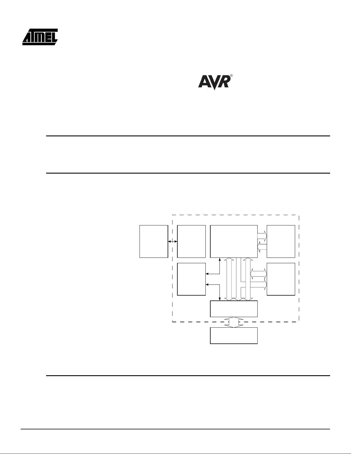
The AVR ATasicICE POD is an ex tension to the AVR ATasicICE (ASIC ICE) wh ich
gives a quick start ASIC development platform for the AVR ASIC users. The ASIC POD
includes two example designs to demonstrate the interface between the AVR core and
the custom logic.
The ASIC ICE POD is bas ed on a fiel d programmable g ate array ( FPGA) that c an be
programmed to function as a custom I/O logic for the AVR core. A set of 64 I/O pins from
the FPGA are made available to the user through connectors. In addition, the ASIC ICE
POD includes SRAM, RS232 ports, and a clock oscillator as on-board resources.
Figure 1-1.
ASIC ICE POD Bl ock Diagram
AVR ATASICICE
HOST PC
W/ AVR
STUDIO
HOST
INTERFACE
CLOCK
GENERATION
LOGIC
AVR V2 CORE
ADR
CTRL
DBUS
PROGRAM
MEMORY
INTERNAL
DATA
MEMORY
This document describes how to configure the FPGA and to use the on-board resources
to the ASIC ICE POD. The ASIC ICE interface is d escribed in the ICEPRO ASIC
Designer’s Guide together with the example designs.
1.2 Power Supply
ATasicICE POD User Guide 1
It is recommended t o u se the emulator power supp ly wh ich i s av ailable on the pod connector. This is done by adding a jumper to the JP2 pins (default setting, see Figure 1-2).
Total current drawn from the emulator must not exceed 1A (@ 5V). At higher currents
POD INTERFACE
POD
Page 3
ATasicICE POD User Guide
M1
M1M0
M2
M2
M0
JP4
www.BDTIC.com/ATMEL
external power should be used instead. When using an external power supply the
jumper at JP2 must be removed.
WARNING! When using external power, the emulator must be switched on before the
external power supply is connected. The external power must be switched off before the
emulator is switched off.
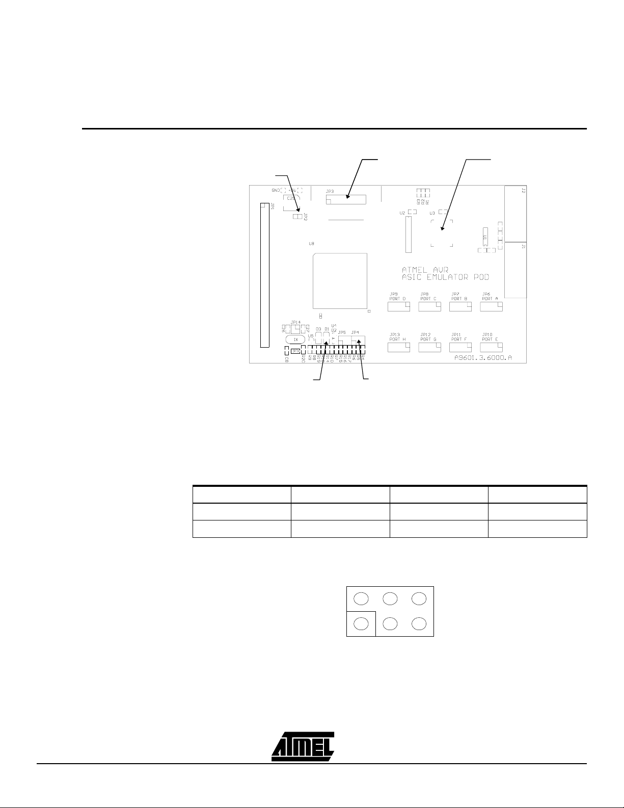
1.3 FPGA
Configuration
Figure 1-2.
POD, FPGA Configuration
EXTERNAL
POWER
CONFIG DONE
LED
XCHECKER
XCHECKER
CONNECTOR
CONNECTOR
MODE SELECT
FPGA CONFIG.
MEMORY
The FPGA can be configured either by using an XChecker cable or a FLASH memory
containing the configuration data. Figure 1-2 shows the pod’s location of the XChecker
cable connector, the PLCC socket for the FLASH memory and the mode select jumpers.
The (green) conf igur ation DON E LED wi ll be li t if the configur atio n proces s is suc cessful.
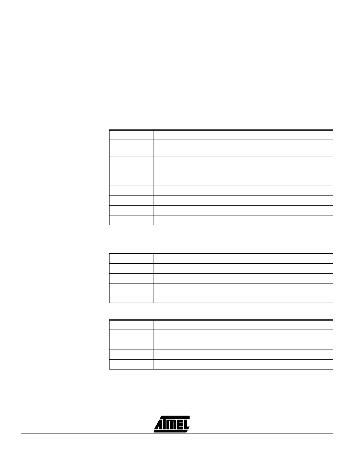
1.3.1 Configuration Mode
Selection
The mode select jumpers (JP4) must be installed according to the following table:
Source M0 M1 M2
XChecker - - FLASH X X -
Note: (X = Jumper inserted, - = No jumper inserted)
Figure 1-3.
Mode Select Jumper Pin-Out
2 ATasicICE POD User Guide
Page 4
ATasicICE POD User Guide
www.BDTIC.com/ATMEL
1.3.2 Configuration Using
the XChecker Cable
1.3.3 Configuration Using
FLASH
1.3.4 FPGA ASIC ICE
Interface Pin-out
Disconnect any power sources connected to the pod and turn off the emulator. Connect
the XChecker cable directly to the XChecker connector on the pod. It is not necessary to
use the flying lead connectors supplied with the XChecker. Supply power and start the
downloading from the XChecker download utility.
WARNING! If the XChecker cable is used to configure the FPGA, the FLASH must be
removed from the socket.
Generate a binary file from the bit configura tion file using the Xilinx makepro m utility.
Use this file to progra m th e FLA SH in a de vi ce progr a mme r. Sup porte d FLA SH dev ic es
are: AT29C010-JC, AT29 C010 A- J C and AT2 9C02 0- JC . Disc onn ec t an y p ower sources
connected to the pod and turn off the emulator. Insert the programmed flash into the
configuration socket on the pod and set the configuration mode jumpers.
Memory Signals
Signal Name FPGA pin-out (physical pin number)
ADR 15:0 = {237, 235, 231, 229, 226, 224, 218, 216, 236, 234, 230, 228, 225, 223,
217, 215}
DBUS 7:0 = {13, 12, 11, 10, 9, 8, 5, 4}
XRAMRE = {23}
XRAMWE = {24}
IORE = {25}
IOWE = {26}
MRAMACK = {27}
CPUWAIT = {34}
Note: Pin numbering = {MSB,..., LSB}
System (Reset / Instruction) Signals
Signal Name FPGA pin-out (physical pin number)
ARESET
IRESET = {20}
SLEEPI = {16}
WDRI = {18}
Interrupt Signals
Signal Name FPGA pin-out (physical pin number)
IRQ 4:0 = {50, 49, 48, 47, 46}
IRQACK = {51}
GLOBINT = {52}
IRQOK = {53}
Note: Pin numbering = {MSB,..., LSB}
= {15}
ATasicICE POD User Guide 3
Page 5
ATasicICE POD User Guide
www.BDTIC.com/ATMEL
Extended Signals (Reserved For Future Use)
Signal Name FPGA pin-out (physical pin number)
IOEXTEND 4:0 = {43, 42, 41, 39, 38}
Note: Pin numbering = {MSB,..., LSB}
Clocks
Signal Name FPGA pin-out (physical pin number)
CLKALWAYS = {57}
EXTCLKIN = {not connected to the FPGA}
EXTCLKEN = {not connected to the FPGA}
CLKRUN = {31}
CLKOSC = {63}
CLKIO = {118}
CLKSTOPIO = {32}
CLKSTOPCORE = {33}
CLKEN = {44}
IOBUSY = {28}
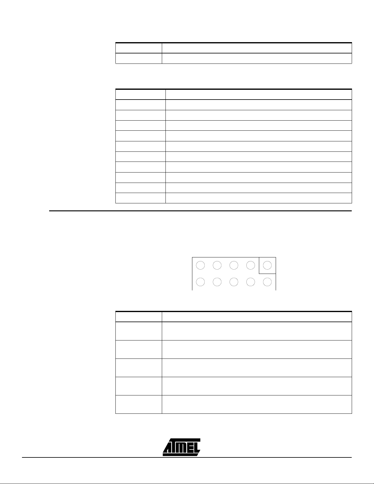
1.4 General I/O Ports
The general I/O por t conne ctors ar e labeled P ORTA-P ORTH on th e pod ca rd. Th ese
ports are direct ly conne cted to th e FPGA. E ach port h as eigh t I/O pins an d two groun d
pins. Short cables should be used when connecting additional logic on the port pins.
Figure 1-4.
Port Connector Pin-Out
PORTx
06
2
GND
WARNING!
The general I/O ports are sensitive to electrostatic discharges.
Ports
Signal Name FPGA pin-out (physical pin number)
PORTA 7:0
(GIO 7:0)
PORTB 7:0
(GIO 15:8)
PORTC 7:0
(GIO 23:16)
PORTD 7:0
(GIO 31:24)
= {167, 168, 169, 170, 171, 172, 175, 176}
= {155, 156, 157, 160, 162, 163, 164, 165}
= {142, 144, 145, 146, 147, 149, 153, 154}
= {131, 132, 133, 134, 136, 137, 138, 139}
4
7GND 1
3
5
PORTE 7:0
(GIO 39:32)
= {116, 117, 124, 125, 126, 127, 128, 130}
4 ATasicICE POD User Guide
Page 6

Ports (Continued)
POWER SRAM RS232 PORTS
EXTERNAL
GENERAL I/O
www.BDTIC.com/ATMEL
Signal Name FPGA pin-out (physical pin number)
ATasicICE POD User Guide
1.5 ASIC POD
Resources
PORTF 7:0
(GIO 47:40)
PORTG 7:0
(GIO 55:48)
PORTH 7:0
(GIO 63:56)
Note: Pin numbering = {MSB,..., LSB}
Figure 1-5.
= {108, 109, 110, 111, 112, 113, 114, 115}
= {97, 99, 100, 102, 103, 104, 105, 107}
= {86, 87, 88, 92, 93, 94, 95, 96}
Pod, On-Board Resources
OSCILLATOR
1.5.1 SRAM (128K bytes)
ATasicICE POD User Guide 5
The ASIC POD includes a 128K bytes SRAM which can be used as external memory to
the AVR core or as general purpose memory. The memory used is a standard asynchronous SRAM with a maximum 20 ns access /cycl e time. The p in-out to the FP GA for
the memory interface is shown below.
Signal Name FPGA pin-out (physical pin number)
(F)ADR 16:0
(F)DAT 7:0 = {123, 129, 141, 148, 152, 159, 173, 177}
(GSRAM)CS\ = {191}
(GSRAM)OE\ = {190}
(GSRAM)WE\ = {189}
Note: Pin numbering = {MSB,..., LSB}
= {2, 239, 238, 233, 232, 221 , 220 , 214 , 21 3, 21 0, 2 09, 203, 202, 188, 187,
184, 183}
Page 7

ATasicICE POD User Guide
www.BDTIC.com/ATMEL
1.5.2 RS232 Ports Both RS232 ports use a 9-pin DSUB connector. An one-to-one serial cable should be
used when connecting the RS232 port to a COM port on a PC.
Signal Name FPGA pin-out (physical pin number)
RxD0 (J1) = {200}
TxD0 (J1) = {198}
RxD1 (J2) = {199}
TxD1 (J2) = {197}
1.5.3 Crystal Oscillator The crystal oscillator is connected to the emulator’s external clock input. To use this
oscillator as c lo ck sou r ce, c hoo se E xte r nal Cl oc k in th e E mu lat or O pti ons men u i n AV R
Studio. A yellow LED (D3) will be lit when the oscillator is selected. The oscillator supports crystals with ope ratin g freq uenc y fr om 10 kH z to 10 MHz . The dif ferent ope ratin g
frequency ranges and their jumper setting (JP5) is shown in the table below.
Figure 1-6.
Oscillator Select Jumper Pin-Out
JP5
F2
F1
EN
F2F1
EN
Output Range F(REQ)1 F(REQ)2 EN(ABLE)
10 kHz - 100 kHz - - 100 kHz - 1 MHz - X 1 MHz - 5 MHz X - 5 MHz - 10 MHz X X High Imped ance (any) (any) X
Note: X = Jumper inserted, - = No jumper inserted
For the lowest frequency r ange, the load c apacitor s has to be disabl ed. This is don e by
removing the jumpers at JP14.
6 ATasicICE POD User Guide
Page 8

1.6 Appendix A:
www.BDTIC.com/ATMEL
ICEPRO ASIC
POD - FPGA
Pinout
ATasicICE POD User Guide
Pin no. on
240-PQFP Emulator Signal Names Comments User Define
1GNDGND
2 FADR16 XRAMADR
3 FADR17 XRAMADR
4 DBUS0 Connector
5 DBUS1 Connector
6 NC Not connected
7 NC Not connected
8 DBUS2 Connector
9 DBUS3 Connector
10 DBUS4 Connector
11 DBUS5 Connector
12 DBUS6 Connector
13 DBUS7 Connector
14 GND GND
15 ARESET Connector
16 SLEEPI Connector
17 NC Not connected
18 WDRI Connector
19 VDD VDD
20 IRESET Connector
21 NC Not connected
22 GND GND
23 XRAMRE Connector
24 XRAMWE Connector
25 IORE Connector
26 IOWE Connector
27 MRAMACK Connector
28 IOBUSY Connector
29 GND GND
30 VDD VDD
31 CLKRUN Connector
32 CLKSTOPIO Connector
33 CLKSTOPCORE Connector
34 CPUWAIT Connector
35 NC Not connected
ATasicICE POD User Guide 7
Page 9

ATasicICE POD User Guide
www.BDTIC.com/ATMEL
Pin no. on
240-PQFP Emulator Signal Names Comments User Define
36 NC Not connected
37 GND GND
38 EXTENDIO0 Connector
39 EXTENDIO1 Connector
40 VDD VDD
41 EXTENDIO2 Connector
42 EXTENDIO3 Connector
43 EXTENDIO4 Connector
44 CLKEN Connector
45 GND GND
46 IRQ0 Connector
47 IRQ1 Connector
48 IRQ2 Connector
49 IRQ3 Connector
50 IRQ4 Connector
51 IRQACK Connector
52 GLOBINT Connector
53 IRQOK Connector
54 NC Not connected
55 NC Not connected
56 NC Not connected
57 CLKALWAYS Connector
58 M1 CONFIG
59 GND GND
60 M0 CONFIG
61 VDD VDD
62 M2 CONFIG
63 CLKOSC Connector
64 TP3/HDC CONFIG
65 NC Not connected
66 NC Not connected
67 NC Not connected
68 TP4/LDC CONFIG
69 NC Not connected
70 NC Not connected
71 NC Not connected
72 NC Not connected
8 ATasicICE POD User Guide
Page 10

ATasicICE POD User Guide
www.BDTIC.com/ATMEL
Pin no. on
240-PQFP Emulator Signal Names Comments User Define
73 NC Not connected
74 NC Not connected
75 GND GND
76 NC Not connected
77 NC Not connected
78 NC Not connected
79 NC Not connected
80 VDD VDD
81 NC Not connected
82 NC Not connected
83 GND GND
84 NC Not connected
85 NC Not connected
86 FIO63 General I/O
87 FIO62 General I/O
88 FI061 General I/O
89 INIT
90 VDD VDD
91 GND GND
92 FIO60 General I/O
93 FIO59 General I/O
94 FIO58 General I/O
95 FIO57 General I/O
96 FIO56 General I/O
97 FIO55 General I/O
98 GND GND
99 FIO54 General I/O
100 FIO53 Genera l I/O
101 VDD VDD
102 FIO52 Genera l I/O
103 FIO51 Genera l I/O
104 FIO50 Genera l I/O
CONFIG
105 FIO49 Genera l I/O
106 GND GND
107 FIO48 Genera l I/O
108 FIO47 Genera l I/O
109 FIO46 Genera l I/O
ATasicICE POD User Guide 9
Page 11

ATasicICE POD User Guide
www.BDTIC.com/ATMEL
Pin no. on
240-PQFP Emulator Signal Names Comments User Define
110 FIO45 Genera l I/O
111 FIO44 Genera l I/O
112 FIO43 Genera l I/O
113 FIO42 Genera l I/O
114 FIO41 Genera l I/O
115 FIO40 Genera l I/O
116 FIO39 Genera l I/O
117 FIO38 Genera l I/O
118 CLKIO Connector
119 GND GND
120 DONE CONFIG
121 VDD VDD
122 PROGRAM CO NFIG
123 FDAT7 XRAMDATA
124 FIO37 Genera l I/O
125 FIO36 Genera l I/O
126 FIO35 Genera l I/O
127 FIO34 Genera l I/O
128 FIO33 Genera l I/O
129 FDAT6 XRAMDATA
130 FIO32 Genera l I/O
131 FIO31 Genera l I/O
132 FIO30 Genera l I/O
133 FIO29 Genera l I/O
134 FIO28 Genera l I/O
135 GND GND
136 FIO27 Genera l I/O
137 FIO26 Genera l I/O
138 FIO25 Genera l I/O
139 FIO24 Genera l I/O
140 VDD VDD
141 FDAT5 XRAMDATA
142 FIO23 Genera l I/O
143 GND GND
144 FIO22 Genera l I/O
145 FIO21 Genera l I/O
146 FIO20 Genera l I/O
10 ATasicICE POD User Guide
Page 12

ATasicICE POD User Guide
www.BDTIC.com/ATMEL
Pin no. on
240-PQFP Emulator Signal Names Comments User Define
147 FIO19 Genera l I/O
148 FDAT4 XRAMDATA
149 FIO18 Genera l I/O
150 VDD VDD
151 GND GND
152 FDAT3 XRAMDATA
153 FIO17 Genera l I/O
154 FIO16 Genera l I/O
155 FIO15 Genera l I/O
156 FIO14 Genera l I/O
157 FIO13 Genera l I/O
158 GND GND
159 FDAT2 General I/O
160 FIO12 XRAMDATA
161 VDD VDD
162 FIO11 General I/O
163 FIO10 General I/O
164 FIO9 General I/O
165 FIO8 General I/O
166 GND GND
167 FIO7 General I/O
168 FIO6 General I/O
169 FIO5 General I/O
170 FIO4 General I/O
171 FIO3 General I/O
172 FIO2 General I/O
173 FDAT1 XRAMDATA
174 NC Not connected
175 FIO1 General I/O
176 FIO0 General I/O
177 FDAT0 XRAMDATA
178 NC Not connected
179 CCLK CONFIG
180 VDD VDD
181 NC Not connected
182 GND GND
183 FADR0 XRAMADR
ATasicICE POD User Guide 11
Page 13

ATasicICE POD User Guide
www.BDTIC.com/ATMEL
Pin no. on
240-PQFP Emulator Signal Names Comments User Define
184 FADR1 XRAMADR
185 NC Not connected
186 NC Not connected
187 FADR3 XRAMADR
188 FADR4 XRAMADR
189 CSRAMWE
190 CSRAMOE XRAMCTRL
191 CSRAMCS
192 NC Not connected
193 NC Not connected
194 NC Not connected
195 NC Not connected
196 GND GND
197 TxD1 UART1
198 TxD0 UART0
199 RxD1 UART1
200 RxD0 UART0
201 VDD VDD
202 FADR5 XRAMADR
203 FADR4 XRAMADR
204 GND GND
205 NC Not connected
206 NC Not connected
XRAMCTRL
XRAMCTRL
207 NC Not connected
208 NC Not connected
209 FADR6 XRAMADR
210 FADR7 XRAMADR
211 GND GND
212 VDD VDD
213 FADR8 XRAMADR
214 FADR9 XRAMADR
215 ADR0 Connector
216 ADR8 Connector
217 ADR1 Connector
218 ADR9 Connector
219 GND GND
220 FADR10 XRAMADR
12 ATasicICE POD User Guide
Page 14

ATasicICE POD User Guide
www.BDTIC.com/ATMEL
Pin no. on
240-PQFP Emulator Signal Names Comments User Define
221 FADR11 XRAMADR
222 VDD VDD
223 ADR2 Connector
224 ADR10 Connector
225 ADR3 Connector
226 ADR11 Connector
227 GND GND
228 ADR4 Connector
229 ADR12 Connector
230 ADR5 Connector
231 ADR13 Connector
232 FADR12 XRAMADR
233 FADR13 XRAMADR
234 ADR6 Connector
235 ADR14 Connector
236 ADR7 Connector
237 ADR15 Connector
238 FADR14 XRAMADR
239 FADR15 XRAMADR
240 VDD VDD
ATasicICE POD User Guide 13
 Loading...