

Atmel AVR AT90S4434, AVR AT90LS4434, AVR AT90LS8535, AVR AT90S8535 Preliminary
Features
®
• AVR
• Data and Nonvolatile Program Memories
• Peripheral Features
• Special Microcontroller Features
• Power Consumption at 4 MHz, 3V, 20°C
• I/O and Packages
• Operating Voltages
• Speed Grades:
– High-performance and Low-power RISC Architecture
– 118 Powerful Instructions – Most Single Clock Cycle Execution
– 32 x 8 General-purpose Working Registers
– Up to 8 MIPS Throughput at 8 MHz
– 4K/8K Bytes of In-System Programmable Flash
SPI Serial Interface for In-System Programming
Endurance: 1,000 Write/Erase Cycles
– 256/512 Bytes EEPROM
Endurance: 100,000 Write/Erase Cycles
– 256/512 Bytes Internal SRAM
– Programming Lock for Software Security
– 8-channel, 10-bit ADC
– Programmable UART
– Master/Slave SPI Serial Interface
– Two 8-bit Timer/Counters with Separate Prescaler and Compare Mode
– One 16-bit Timer/Counter with Separate Prescaler, Compare and
Capture Modes and Dual 8-, 9- or 10-bit PWM
– Programmable Watchdog Timer with On-chip Oscillator
– On-chip Analog Comparator
– Power-on Reset Circuit
– Real-time Clock (RTC) with Separate Oscillator and Counter Mode
– External and Internal Interrupt Sources
– Three Sleep Modes: Idle, Power Save and Power-down
– Active: 6.4 mA
– Idle Mode: 1.9 mA
– Power-down Mode: <1 µA
– 32 Programmable I/O Lines
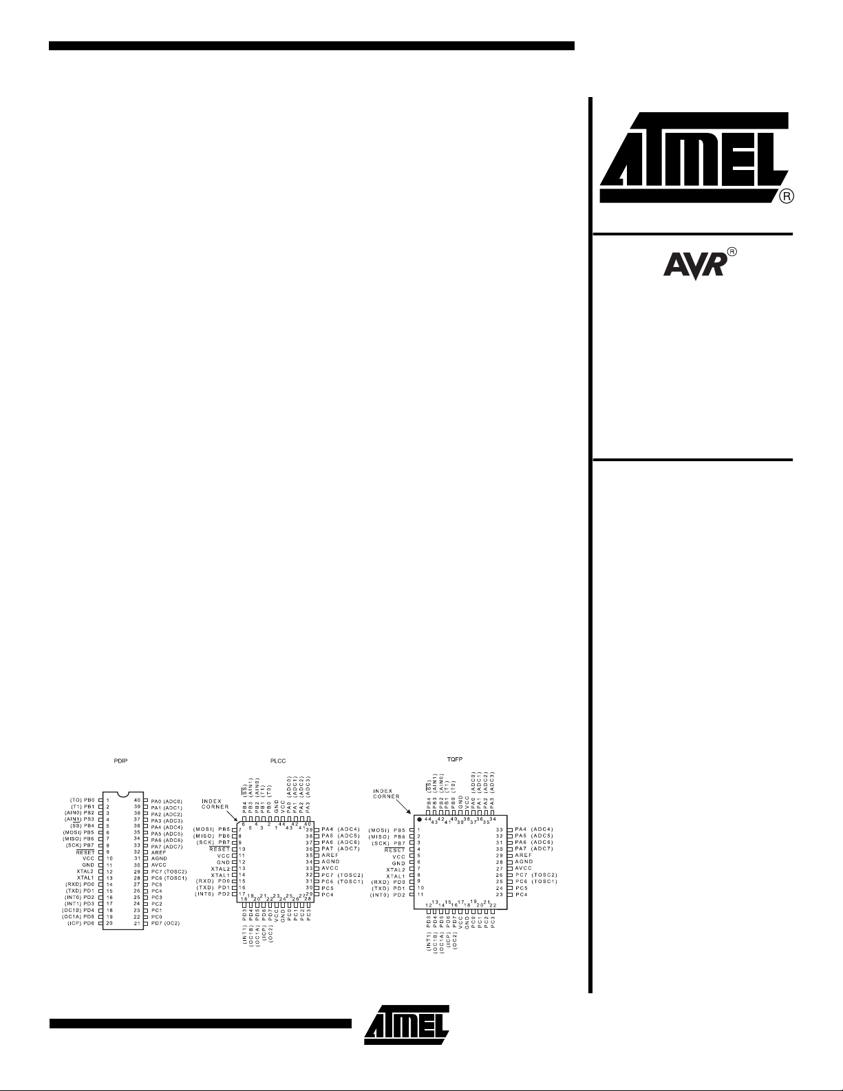
– 40-pin PDIP, 44-pin PLCC and 44-pin TQFP
–V
: 4.0 - 6.0V AT90S4434/AT90S8535
CC
: 2.7 - 6.0V AT90LS4434/AT90LS8535
–V
CC
– 0 - 8 MHz AT90S4434/AT90S8535
– 0 - 4 MHz AT90LS4434/AT90LS8535
8-bit
Microcontroller
with 4K/8K
Bytes In-System
Programmable
Flash
AT90S4434
AT90LS4434
AT90S8535
AT90LS8535
Preliminary
Pin Configurations
Rev. 1041F–10/00
1
Description
The AT90S4434/8535 is a low-power CMOS 8-bit microcontroller based on the AVR RISC architecture. By executing powerful instructions in a single clock cycle, the AT90S4434/8535 achieves throughputs approaching 1 MIPS per MHz allowing
the system designer to optimize power consumption versus processing speed.
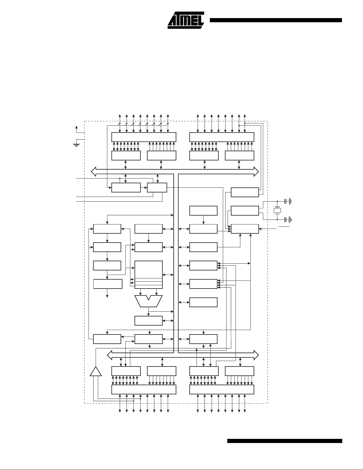
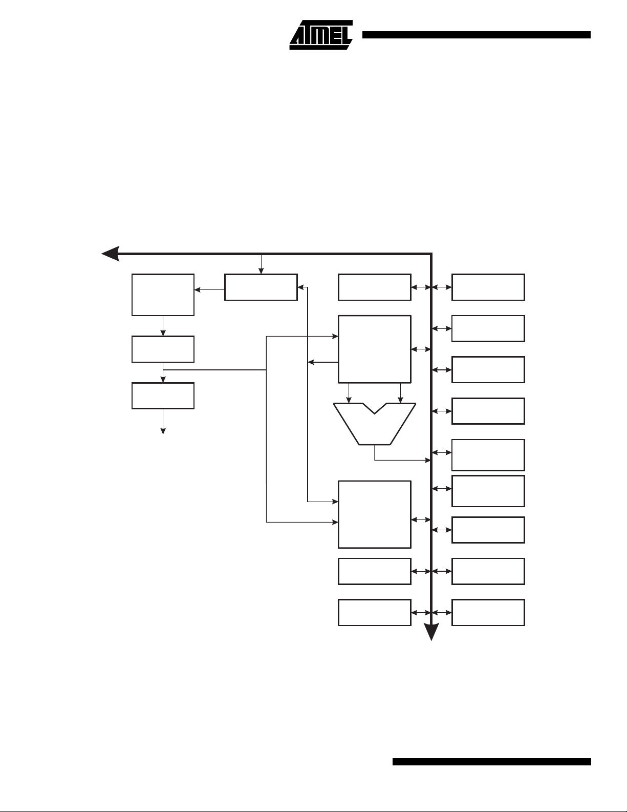
Block Diagram
Figure 1. The AT90S4434/8535 Block Diagram
PA0 - PA7
VCC
PC0 - PC7
GND
AVCC
AGND
AREF
DATA REGISTER
PROGRAM
COUNTER
PROGRAM
FLASH
INSTRUCTION
REGISTER
INSTRUCTION
DECODER
CONTROL
LINES
PORTA DRIVERS
DATA DIR.
PORTA
ANALOG MUX ADC
REG. PORTA
STACK
POINTER
SRAM
GENERAL
PURPOSE
REGISTERS
X
Y
Z
ALU
8-BIT DATA BUS
PORTC DRIVERS
DATA REGISTER
PORTC
INTERNAL
OSCILLATOR
WATCHDOG
TIMER
MCU CONTROL
REGISTER
TIMER/
COUNTERS
INTERRUPT
UNIT
EEPROM
DATA DIR.
REG. PORTC
OSCILLATOR
OSCILLATOR
TIMING AND
CONTROL
XTAL1
XTAL2
RESET
STATUS
REGISTER
PROGRAMMING
LOGIC
DATA REGISTER
ARATOR
ANALOG
COMP
PORTB
+
-
2
AT90S/LS4434 and AT90S/LS8535
SPI
REG. PORTB
PORTB DRIVERS
PB0 - PB7
DATA DIR.
UART
DATA REGISTER
PORTD
PORTD DRIVERS
PD0 - PD7
DATA DIR.
REG. PORTD
AT90S/LS4434 and AT90S/LS8535
The AVR core combines a rich instruction set with 32 general-purpose working registers. All the 32 registers are directly
connected to the Arithmetic Logic Unit (ALU), allowing two independent registers to be accessed in one single instruction
executed in one clock cycle. The resulting architecture is more code efficient while achieving throughputs up to ten times
faster than conventional CISC microcontrollers.
The AT90S4434/8535 provides the following features: 4K/8K bytes of In-System Programmable Flash, 256/512 bytes
EEPROM, 256/512 bytes SRAM, 32 general-purpose I/O lines, 32 general-purpose working registers, Real-time Clock
(RTC), three flexible timer/counters with compare modes, internal and external interrupts, a programmable serial UART,
8-channel, 10-bit ADC, programmable Watchdog Timer with internal oscillator, an SPI serial port and three softwareselectable power-saving modes. The Idle Mode stops the CPU while allowing the SRAM, timer/counters, SPI port and
interrupt system to continue functioning. The Power-down Mode saves the register contents but freezes the oscillator, disabling all other chip functions until the next interrupt or hardware reset. In Power Save Mode, the timer oscillator continues
to run, allowing the user to maintain a timer base while the rest of the device is sleeping.
The device is manufactured using Atmel’s high-density nonvolatile memory technology. The on-chip ISP Flash allows the
program memory to be reprogrammed in-system through an SPI serial interface or by a conventional nonvolatile memory
programmer. By combining an 8-bit RISC CPU with In-System Programmable Flash on a monolithic chip, the Atmel
AT90S4434/8535 is a powerful microcontroller that provides a highly flexible and cost effective solution to many embedded
control applications.
The AT90S4434/8535 AVR is supported with a full suite of program and system development tools including: C compilers,
macro assemblers, program debugger/simulators, in-circuit emulators and evaluation kits.
Comparison between AT90S4434 and AT90S8535
The AT90S4434 has 4K bytes of In-System Programmable Flash, 256 bytes of EEPROM and 256 bytes of internal SRAM.
The AT90S8535 has 8K bytes of In-System Programmable Flash, 512 bytes of EEPROM and 512 bytes of internal SRAM.
Table 1 summarizes the different memory sizes for the two devices.
Table 1. Memory Size Summary
Part Flash EEPROM SRAM
AT90S4434 4K bytes 256 bytes 256 bytes
AT90S8535 8K bytes 512 bytes 512 bytes
Pin Descriptions
VCC
Digital supply voltage
GND
Digital ground
Port A (PA7..PA0)
Port A is an 8-bit bi-directional I/O port. Port pins can provide internal pull-up resistors (selected for each bit). The Port A
output buffers can sink 20 mA and can drive LED displays directly. When pins PA0 to PA7 are used as inputs and are
externally pulled low, they will source current if the internal pull-up resistors are activated.
Port A also serves as the analog inputs to the A/D Converter.
The Port A pins are tri-stated when a reset condition becomes active, even if the clock is not running.
Port B (PB7..PB0)
Port B is an 8-bit bi-directional I/O port with internal pull-up resistors. The Port B output buffers can sink 20 mA. As inputs,
Port B pins that are externally pulled low will source current if the pull-up resistors are activated. Port B also serves the
functions of various special features of the AT90S4434/8535 as listed on page 71.
3

The Port B pins are tri-stated when a reset condition becomes active, even if the clock is not running.
Port C (PC7..PC0)
Port C is an 8-bit bi-directional I/O port with internal pull-up resistors. The Port C output buffers can sink 20 mA. As inputs,
Port C pins that are externally pulled low will source current if the pull-up resistors are activated. Two Port C pins can alternatively be used as oscillator for Timer/Counter2.
The Port C pins are tri-stated when a reset condition becomes active, even if the clock is not running.
Port D (PD7..PD0)
Port D is an 8-bit bi-directional I/O port with internal pull-up resistors. The Port D output buffers can sink 20 mA. As inputs,
Port D pins that are externally pulled low will source current if the pull-up resistors are activated.
Port D also serves the functions of various special features of the AT90S4434/8535 as listed on page 79.
The Port D pins are tri-stated when a reset condition becomes active, even if the clock is not running.
RESET
Reset input. An external reset is generated by a low level on the RESET pin. Reset pulses longer than 50 ns will generate
a reset, even if the clock is not running. Shorter pulses are not guaranteed to generate a reset.
XTAL1
Input to the inverting oscillator amplifier and input to the internal clock operating circuit.
XTAL2
Output from the inverting oscillator amplifier.
AVCC
This is the supply voltage pin for Port A and the A/D Converter. If the ADC is not used, this pin must be connected to VCC.
If the ADC is used, this pin must be connected to VCC via a low-pass filter. See page 61 for details on operation of the
ADC.
AREF
This is the analog reference input for the A/D Converter. For ADC operations, a voltage in the range 2V to AV
applied to this pin.
AGND
Analog ground. If the board has a separate analog ground plane, this pin should be connected to this ground plane. Otherwise, connect to GND.
must be
CC
4
AT90S/LS4434 and AT90S/LS8535
AT90S/LS4434 and AT90S/LS8535
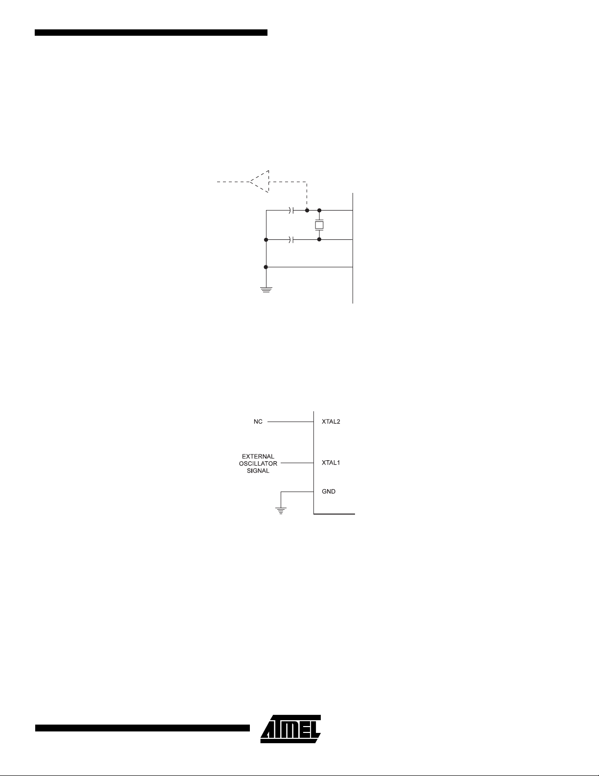
Clock Options
Crystal Oscillator
XTAL1 and XTAL2 are input and output, respectively, of an inverting amplifier which can be configured for use as an
on-chip oscillator, as shown in Figure 2. Either a quartz crystal or a ceramic resonator may be used.
Figure 2. Oscillator Connections
MAX 1 HC BUFFER
HC
C2
C1
Note: When using the MCU Oscillator as a clock for an external device, an HC buffer should be connected as indicated in the figure.
External Clock
To drive the device from an external clock source, XTAL2 should be left unconnected while XTAL1 is driven as shown in
Figure 3.
Figure 3. External Clock Drive Configuration
XTAL2
XTAL1
GND
Timer Oscillator
For the Timer Oscillator pins, PC6(TOSC1) and PC7(TOSC2), the crystal is connected directly between the pins. No external capacitors are needed. The oscillator is optimized for use with a 32,768 Hz watch crystal. An external clock signal
applied to TOSC1 goes through the same amplifier having a bandwidth of 256 kHz. The external clock signal should therefore be in the interval 0 Hz - 256 kHz.
5
Architectural Overview
The fast-access register file concept contains 32 x 8-bit general-purpose working registers with a single clock cycle access
time. This means that during one single clock cycle, one Arithmetic Logic Unit (ALU) operation is executed. Two operands
are output from the register file, the operation is executed and the result is stored back in the register file – in one clock
cycle.
Six of the 32 registers can be used as three 16-bit indirect address register pointers for Data Space addressing, enabling
efficient address calculations. One of the three address pointers is also used as the address pointer for the constant table
look-up function. These added function registers are the 16-bit X-register, Y-register and Z-register.
Figure 4. The AT90S4434/8535 AVR RISC Architecture
AVR
2K/4K X 16
Program
Memory
Instruction
Register
Instruction
Decoder
Control Lines
AT90S4434/8535 Architecture
Data Bus 8-bit
Program
Counter
Direct Addressing
Indirect Addressing
Status
and Control
32 x 8
General
Purpose
Registrers
ALU
256/512 x 8
Data
SRAM
Interrupt
Unit
SPI
Unit
Serial
UART
8-bit
Timer/Counter
16-bit
Timer/Counter
with PWM
8-bit
Timer/Counter
with PWM
Watchdog
Timer
256/512 x 8
EEPROM
32
I/O Lines
Analog to Digital
Converter
Analog
Comparator
The ALU supports arithmetic and logic functions between registers or between a constant and a register. Single register
operations are also executed in the ALU. Figure 4 shows the AT90S4434/8535 AVR RISC microcontroller architecture.
In addition to the register operation, the conventional memory addressing modes can be used on the register file as well.
This is enabled by the fact that the register file is assigned the 32 lowermost Data Space addresses ($00 - $1F), allowing
them to be accessed as though they were ordinary memory locations.
6
AT90S/LS4434 and AT90S/LS8535

AT90S/LS4434 and AT90S/LS8535
The I/O memory space contains 64 addresses for CPU peripheral functions as Control Registers, Timer/Counters, A/D
converters and other I/O functions. The I/O memory can be accessed directly or as the Data Space locations following
those of the register file, $20 - $5F.
The AVR uses a Harvard architecture concept – with separate memories and buses for program and data. The program
memory is executed with a two-stage pipeline. While one instruction is being executed, the next instruction is pre-fetched
from the program memory. This concept enables instructions to be executed in every clock cycle. The program memory is
in-system downloadable Flash memory.
With the relative jump and call instructions, the whole 2K/4K address space is directly accessed. Most AVR instructions
have a single 16-bit word format. Every program memory address contains a 16- or 32-bit instruction.
During interrupts and subroutine calls, the return address Program Counter (PC) is stored on the stack. The stack is effectively allocated in the general data SRAM and consequently, the stack size is only limited by the total SRAM size and the
usage of the SRAM. All user programs must initialize the SP in the reset routine (before subroutines or interrupts are
executed). The 9/10-bit stack pointer (SP) is read/write-accessible in the I/O space.
The 256/512 bytes data SRAM can be easily accessed through the five different addressing modes supported in the AVR
architecture.
The memory spaces in the AVR architecture are all linear and regular memory maps.
Figure 5. Memory Maps
Program Flash
(2K/4K x 16)
$000
Data MemoryProgram Memory
32 Gen. Purpose
Working Registers
64 I/O Registers
Internal SRAM
(256/512 x 8)
$0000
$001F
$0020
$005F
$0060
$015F/$025F
Data Memory
$000
EEPROM
(256/512 x 8)
$0FF/$1FF
$7FF/$FFF
A flexible interrupt module has its control registers in the I/O space with an additional global interrupt enable bit in the status
register. All the different interrupts have a separate interrupt vector in the interrupt vector table at the beginning of the program memory. The different interrupts have priority in accordance with their interrupt vector position. The lower the
interrupt vector address, the higher the priority.
7
General-purpose Register File
Figure 6 shows the structure of the 32 general-purpose working registers in the CPU.
Figure 6. AVR CPU General-purpose Working Registers
70Addr.
R0 $00
R1 $01
R2 $02
…
R13 $0D
General R14 $0E
Purpose R15 $0F
Working R16 $10
Registers R17 $11
…
R26 $1A X-register low byte
R27 $1B X-register high byte
R28 $1C Y-register low byte
R29 $1D Y-register high byte
R30 $1E Z-register low byte
R31 $1F Z-register high byte
All the register operating instructions in the instruction set have direct and single-cycle access to all registers. The only
exception is the five constant arithmetic and logic instructions SBCI, SUBI, CPI, ANDI and ORI between a constant and a
register and the LDI instruction for load immediate constant data. These instructions apply to the second half of the registers in the register file (R16..R31). The general SBC, SUB, CP, AND and OR and all other operations between two
registers or on a single register apply to the entire register file.
As shown in Figure 6, each register is also assigned a data memory address, mapping them directly into the first 32 locations of the user Data Space. Although not being physically implemented as SRAM locations, this memory organization
provides great flexibility in access of the registers, as the X, Y and Z registers can be set to index any register in the file.
X-register, Y-register and Z-register
The registers R26..R31 have some added functions to their general-purpose usage. These registers are address pointers
for indirect addressing of the Data Space. The three indirect address registers, X, Y and Z, are defined in Figure 7.
Figure 7. X-, Y- and Z-registers
15 0
X-register 7 0 7 0
R27 ($1B) R26 ($1A)
15 0
Y-register 7 0 7 0
R29 ($1D) R28 ($1C)
15 0
Z-register 7 0 7 0
R31 ($1F) R30 ($1E)
In the different addressing modes, these address registers have functions as fixed displacement, automatic increment and
decrement (see the descriptions for the different instructions).
8
AT90S/LS4434 and AT90S/LS8535
AT90S/LS4434 and AT90S/LS8535
ALU – Arithmetic Logic Unit
The high-performance AVR ALU operates in direct connection with all the 32 general-purpose working registers. Within a
single clock cycle, ALU operations between registers in the register file are executed. The ALU operations are divided into
three main categories: arithmetic, logical and bit functions.
In-System Programmable Flash Program Memory
The AT90S4434/8535 contains 4K/8K bytes on-chip, In-System Programmable Flash memory for program storage. Since
all instructions are 16- or 32-bit words, the Flash is organized as 2K/4K x 16. The Flash memory has an endurance of at
least 1000 write/erase cycles. The AT90S4434/8535 Program Counter (PC) is 11/12 bits wide, thus addressing the
2048/4096 program memory addresses.
See page 93 for a detailed description on Flash data downloading.
See page 10 for the different program memory addressing modes.
SRAM Data Memory
Figure 8 shows how the AT90S4434/8535 SRAM memory is organized.
Figure 8. SRAM Organization
Register File
R0
R1
R2
...
R29
R30
R31
I/O Registers
$00
$01
$02
...
$3D
$3E
$3F
Data Address Space
$0000
$0001
$0002
...
$001D
$001E
$001F
$0020
$0021
$0022
...
$005D
$005E
$005F
Internal SRAM
$0060
$0061
...
$015E/$025E
$015F/$025F
The lower 352/608 data memory locations address the Register file, the I/O memory and the internal data SRAM. The first
96 locations address the Register file + I/O memory, and the next 256/512 locations address the internal data SRAM.
The five different addressing modes for the data memory cover: Direct, Indirect with Displacement, Indirect, Indirect with
Pre-decrement and Indirect with Post-increment. In the register file, registers R26 to R31 feature the indirect addressing
pointer registers.
The direct addressing reaches the entire data space.
The Indirect with Displacement mode features 63 address locations reached from the base address given by the Y- or
Z-registers.
9
When using register indirect addressing modes with automatic pre-decrement and post-increment, the address registers X,
Y and Z are decremented and incremented.
The 32 general-purpose working registers, 64 I/O registers and the 256/512 bytes of internal data SRAM in the
AT90S4434/8535 are all accessible through all these addressing modes.
See the next section for a detailed description of the different addressing modes.
Program and Data Addressing Modes
The AT90S4434/8535 AVR RISC microcontroller supports powerful and efficient addressing modes for access to the program memory (Flash) and data memory (SRAM, register file and I/O memory). This section describes the different
addressing modes supported by the AVR architecture. In the figures, OP means the operation code part of the instruction
word. To simplify, not all figures show the exact location of the addressing bits.
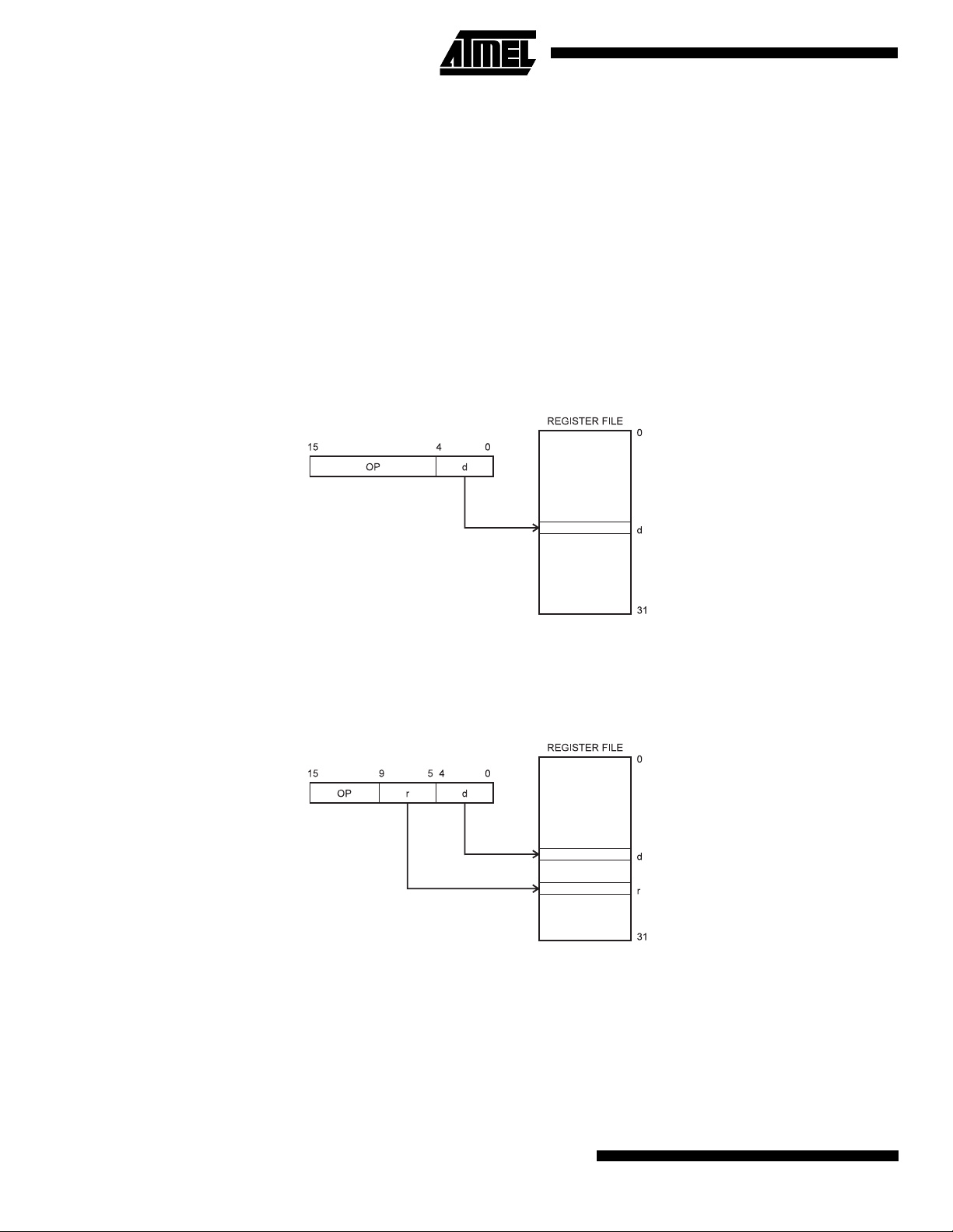
Register Direct, Single Register Rd
Figure 9. Direct Single Register Addressing
The operand is contained in register d (Rd).
Register Direct, Two Registers Rd And Rr
Figure 10. Direct Register Addressing, Two Registers
Operands are contained in register r (Rr) and d (Rd). The result is stored in register d (Rd).
10
AT90S/LS4434 and AT90S/LS8535
AT90S/LS4434 and AT90S/LS8535
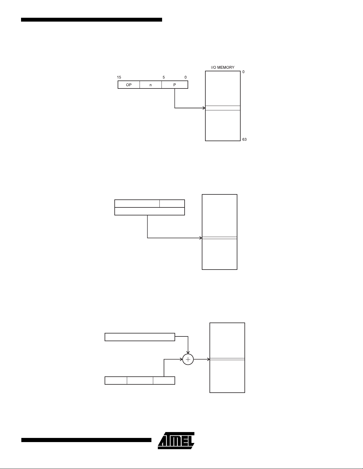
I/O Direct
Figure 11. I/O Direct Addressing
Operand address is contained in six bits of the instruction word. n is the destination or source register address.
Data Direct
Figure 12. Direct Data Addressing
16 LSBs
20 19
16
31
OP Rr/Rd
15 0
Data Space
$0000
$015F/
$025F
A 16-bit data address is contained in the 16 LSBs of a 2-word instruction. Rd/Rr specify the destination or source register.
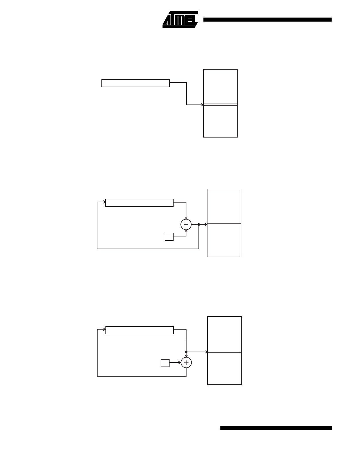
Data Indirect with Displacement
Figure 13. Data Indirect with Displacement
15
15
OP an
Data Space
0
Y OR Z - REGISTER
05610
$0000
$015F/
025F
Operand address is the result of the Y- or Z-register contents added to the address contained in six bits of the instruction
word.
11
Data Indirect
/
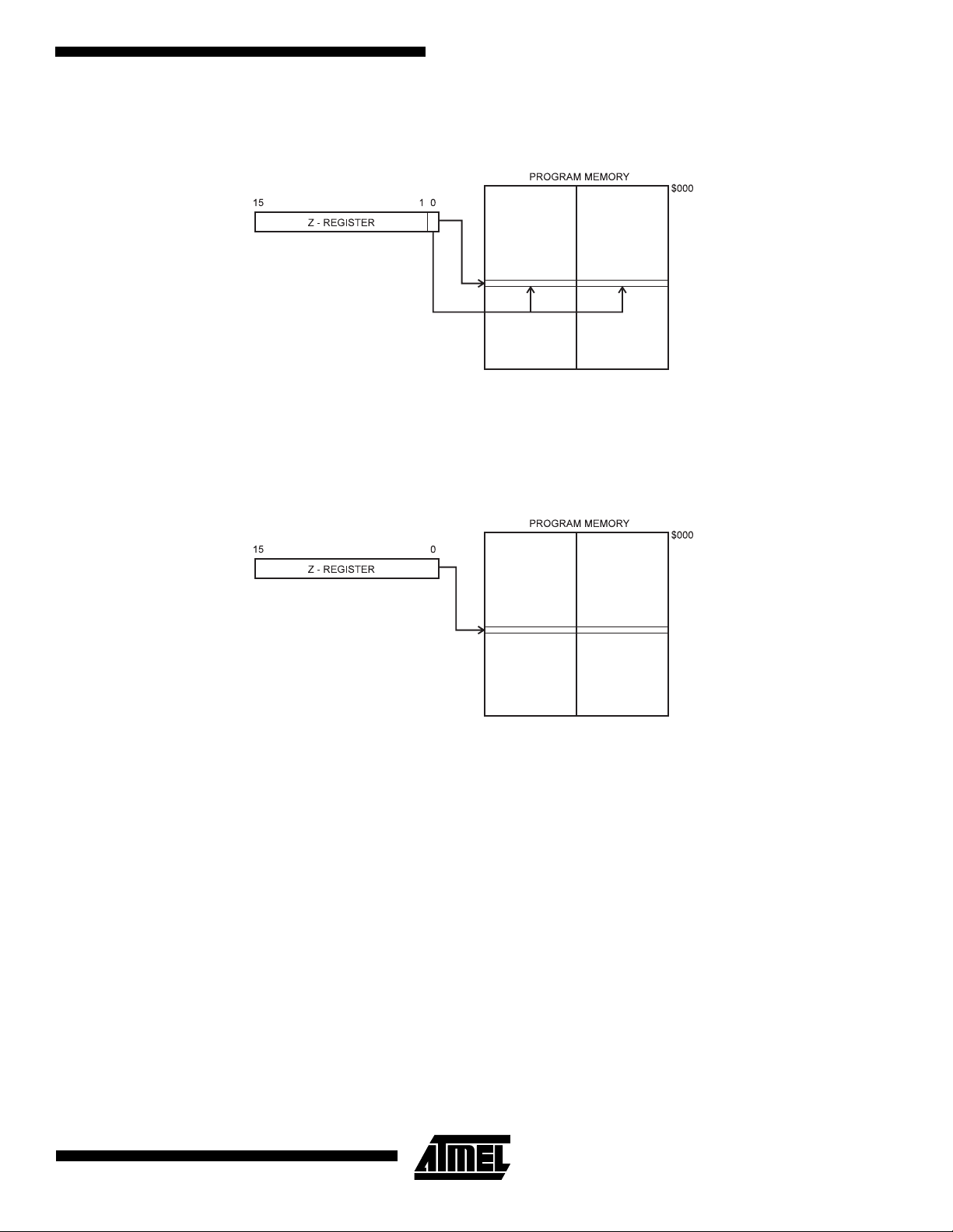
Figure 14. Data Indirect Addressing
015
X, Y OR Z - REGISTER
Operand address is the contents of the X-, Y- or the Z-register.
Data Indirect with Pre-decrement
Figure 15. Data Indirect Addressing with Pre-decrement
015
X, Y OR Z - REGISTER
Data Space
Data Space
$0000
$015F/
$025F
$0000
-1
$015F/
$025F
The X-, Y- or the Z-register is decremented before the operation. Operand address is the decremented contents of the X-,
Y- or the Z-register.
Data Indirect with Post-increment
Figure 16. Data Indirect Addressing with Post-increment
Data Space
015
X, Y OR Z - REGISTER
1
$0000
$015F
$025F
The X-, Y- or the Z-register is incremented after the operation. Operand address is the content of the X-, Y- or the Z-register
prior to incrementing.
12
AT90S/LS4434 and AT90S/LS8535
AT90S/LS4434 and AT90S/LS8535
Constant Addressing Using the LPM Instruction
Figure 17. Code Memory Constant Addressing
$7FF/
$FFF
Constant byte address is specified by the Z-register contents. The 15 MSBs select word address (0 - 2K/4K), the LSB
selects low byte if cleared (LSB = 0) or high byte if set (LSB = 1).
Indirect Program Addressing, IJMP and ICALL
Figure 18. Indirect Program Memory Addressing
$7FF/
$FFF
Program execution continues at address contained by the Z-register (i.e., the PC is loaded with the contents of the
Z-register).
13
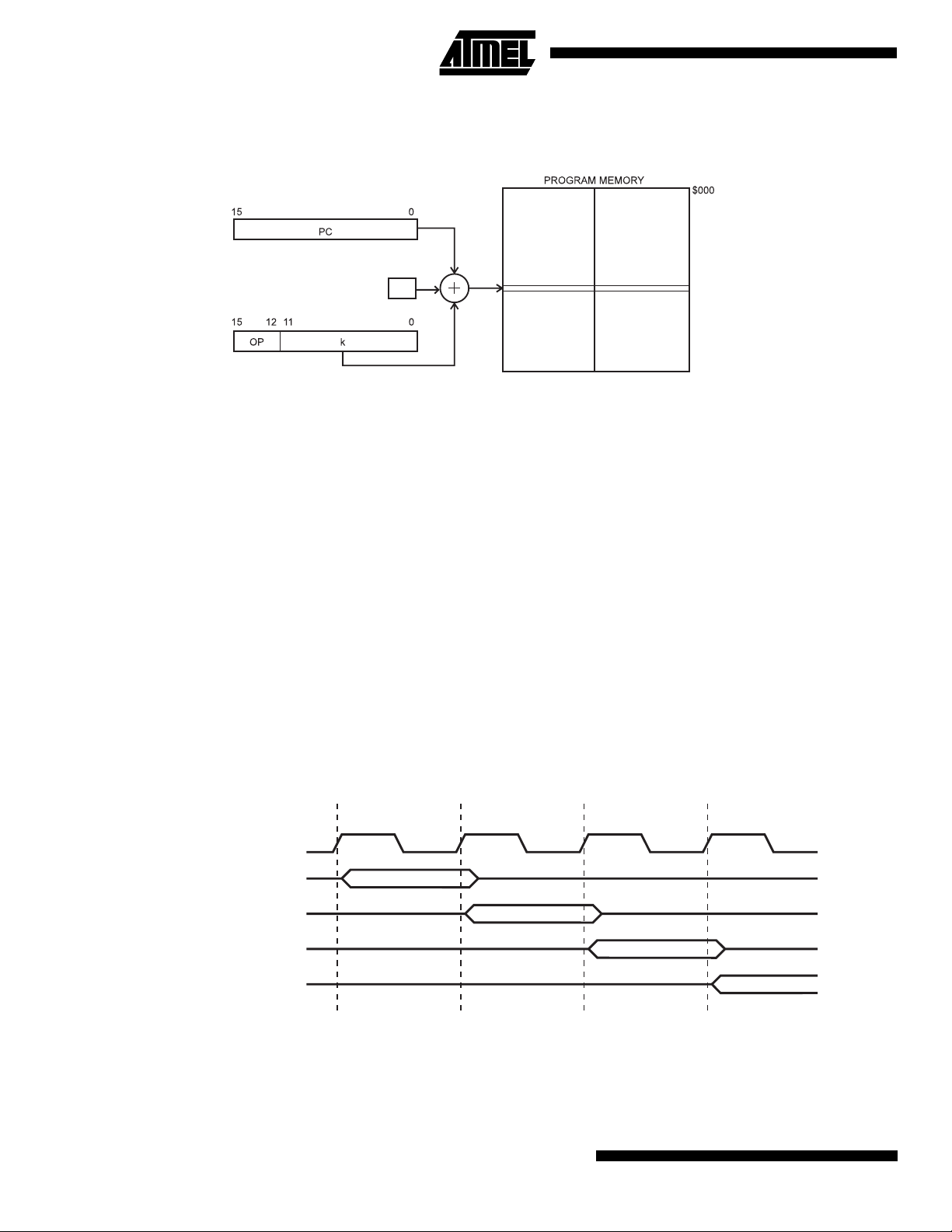
Relative Program Addressing, RJMP and RCALL
Figure 19. Relative Program Memory Addressing
+1
$7FF/
$FFF
Program execution continues at address PC + k + 1. The relative address k is from -2048 to 2047.
EEPROM Data Memory
The AT90S4434/8535 contains 256/512 bytes of data EEPROM memory. It is organized as a separate data space, in
which single bytes can be read and written. The EEPROM has an endurance of at least 100,000 write/erase cycles. The
access between the EEPROM and the CPU is described on page 48 specifying the EEPROM address registers, the
EEPROM data register and the EEPROM control register.
For the SPI data downloading, see page 93 for a detailed description.
Memory Access Times and Instruction Execution Timing
This section describes the general access timing concepts for instruction execution and internal memory access.
The AVR CPU is driven by the System Clock Ø, directly generated from the external clock crystal for the chip. No internal
clock division is used.
Figure 20 shows the parallel instruction fetches and instruction executions enabled by the Harvard architecture and the
fast-access register file concept. This is the basic pipelining concept to obtain up to 1 MIPS per MHz with the corresponding
unique results for functions per cost, functions per clocks and functions per power-unit.
Figure 20. The Parallel Instruction Fetches and Instruction Executions
T1 T2 T3 T4
System Clock Ø
1st Instruction Fetch
1st Instruction Execute
2nd Instruction Fetch
2nd Instruction Execute
3rd Instruction Fetch
3rd Instruction Execute
4th Instruction Fetch
Figure 21 shows the internal timing concept for the register file. In a single clock cycle an ALU operation using two register
operands is executed and the result is stored back to the destination register.
14
AT90S/LS4434 and AT90S/LS8535

AT90S/LS4434 and AT90S/LS8535
Figure 21. Single Cycle ALU Operation
T1 T2 T3 T4
System Clock Ø
Total Execution Time
Register Operands Fetch
ALU Operation Execute
Result Write Back
The internal data SRAM access is performed in two System Clock cycles as described in Figure 22.
Figure 22. On-chip Data SRAM Access Cycles
T1 T2 T3 T4
System Clock Ø
Address
Data
WR
Data
RD
Prev. Address
Address
Write
Read
15

I/O Memory
The I/O space definition of the AT90S4434/8535 is shown in Table 2.
Table 2. AT90S4434/8535 I/O Space
I/O Address (SRAM Address) Name Function
$3F ($5F) SREG Status REGister
$3E ($5E) SPH Stack Pointer High
$3D ($5D) SPL Stack Pointer Low
$3B ($5B) GIMSK General Interrupt MaSK register
$3A ($5A) GIFR General Interrupt Flag Register
$39 ($59) TIMSK Timer/Counter Interrupt MaSK register
$38 ($58) TIFR Timer/Counter Interrupt Flag register
$35 ($55) MCUCR MCU general Control Register
$34 ($45) MCUSR MCU general Status Register
$33 ($53) TCCR0 Timer/Counter0 Control Register
$32 ($52) TCNT0 Timer/Counter0 (8-bit)
$2F ($4F) TCCR1A Timer/Counter1 Control Register A
$2E ($4E) TCCR1B Timer/Counter1 Control Register B
$2D ($4D) TCNT1H Timer/Counter1 High Byte
$2C ($4C) TCNT1L Timer/Counter1 Low Byte
$2B ($4B) OCR1AH Timer/Counter1 Output Compare Register A High Byte
$2A ($4A) OCR1AL Timer/Counter1 Output Compare Register A Low Byte
$29 ($49) OCR1BH Timer/Counter1 Output Compare Register B High Byte
$28 ($48) OCR1BL Timer/Counter1 Output Compare Register B Low Byte
$27 ($47) ICR1H T/C 1 Input Capture Register High Byte
$26 ($46) ICR1L T/C 1 Input Capture Register Low Byte
$25 ($45) TCCR2 Timer/Counter2 Control Register
$24 ($44) TCNT2 Timer/Counter2 (8-bit)
$23 ($43) OCR2 Timer/Counter2 Output Compare Register
$22 ($42) ASSR Asynchronous Mode Status Register
$21 ($41) WDTCR Watchdog Timer Control Register
$1F ($3E) EEARH EEPROM Address Register High Byte
$1E ($3E) EEARL EEPROM Address Register Low Byte
$1D ($3D) EEDR EEPROM Data Register
$1C ($3C) EECR EEPROM Control Register
$1B ($3B) PORTA Data Register, Port A
$1A ($3A) DDRA Data Direction Register, Port A
16
$19 ($39) PINA Input Pins, Port A
$18 ($38) PORTB Data Register, Port B
AT90S/LS4434 and AT90S/LS8535

Table 2. AT90S4434/8535 I/O Space (Continued)
I/O Address (SRAM Address) Name Function
$17 ($37) DDRB Data Direction Register, Port B
$16 ($36) PINB Input Pins, Port B
$15 ($35) PORTC Data Register, Port C
$14 ($34) DDRC Data Direction Register, Port C
$13 ($33) PINC Input Pins, Port C
$12 ($32) PORTD Data Register, Port D
$11 ($31) DDRD Data Direction Register, Port D
$10 ($30) PIND Input Pins, Port D
$0F ($2F) SPDR SPI I/O Data Register
$0E ($2E) SPSR SPI Status Register
$0D ($2D) SPCR SPI Control Register
$0C ($2C) UDR UART I/O Data Register
$0B ($2B) USR UART Status Register
$0A ($2A) UCR UART Control Register
AT90S/LS4434 and AT90S/LS8535
$09 ($29) UBRR UART Baud Rate Register
$08 ($28) ACSR Analog Comparator Control and Status Register
$07 ($27) ADMUX ADC Multiplexer Select Register
$06 ($26) ADCSR ADC Control and Status Register
$05 ($25) ADCH ADC Data Register High
$04 ($24) ADCL ADC Data Register Low
Note: Reserved and unused locations are not shown in the table.
All AT90S4434/8535 I/Os and peripherals are placed in the I/O space. The I/O locations are accessed by the IN and OUT
instructions transferring data between the 32 general-purpose working registers and the I/O space. I/O registers within the
address range $00 - $1F are directly bit-accessible using the SBI and CBI instructions. In these registers, the value of
single bits can be checked by using the SBIS and SBIC instructions. Refer to the instruction set section for more details.
When using the I/O specific commands IN and OUT, the I/O addresses $00 - $3F must be used. When addressing I/O registers as SRAM, $20 must be added to these addresses. All I/O register addresses throughout this document are shown
with the SRAM address in parentheses.
For compatibility with future devices, reserved bits should be written to zero if accessed. Reserved I/O memory addresses
should never be written.
Some of the status flags are cleared by writing a logical “1” to them. Note that the CBI and SBI instructions will operate on
all bits in the I/O register, writing a “1” back into any flag read as set, thus clearing the flag. The CBI and SBI instructions
work with registers $00 to $1F only.
The I/O and peripherals control registers are explained in the following sections.
17
Status Register – SREG
The AVR Status Register (SREG) at I/O space location $3F ($5F) is defined as:
Bit 76543210
$3F ($5F) I T H S V N Z C SREG
Read/Write R/W R/W R/W R/W R/W R/W R/W R/W
Initial value 0 0 0 0 0 0 0 0
Bit 7 – I: Global Interrupt Enable
•
The global interrupt enable bit must be set (one) for the interrupts to be enabled. The individual interrupt enable control is
then performed in separate control registers. If the global interrupt enable register is cleared (zero), none of the interrupts
are enabled independent of the individual interrupt enable settings. The I-bit is cleared by hardware after an interrupt has
occurred and is set by the RETI instruction to enable subsequent interrupts.
Bit 6 – T: Bit Copy Storage
•
The bit copy instructions BLD (Bit LoaD) and BST (Bit STore) use the T-bit as source and destination for the operated bit. A
bit from a register in the register file can be copied into T by the BST instruction and a bit in T can be copied into a bit in a
register in the register file by the BLD instruction.
Bit 5 – H: Half-carry Flag
•
The half-carry flag H indicates a half-carry in some arithmetic operations. See the Instruction Set description for detailed
information.
Bit 4 – S: Sign Bit, S = N⊄⊕ V
•
The S-bit is always an exclusive or between the negative flag N and the two’s complement overflow flag V. See the Instruction Set description for detailed information.
•
Bit 3 – V: Two’s Complement Overflow Flag
The two’s complement overflow flag V supports two’s complement arithmetics. See the Instruction Set description for
detailed information.
Bit 2 – N: Negative Flag
•
The negative flag N indicates a negative result from an arithmetical or logical operation. See the Instruction Set description
for detailed information.
Bit 1 – Z: Zero Flag
•
The zero flag Z indicates a zero result from an arithmetical or logic operation. See the Instruction Set description for
detailed information.
•
Bit 0 – C: Carry Flag
The carry flag C indicates a carry in an arithmetical or logical operation. See the Instruction Set description for detailed
information.
Note that the Status Register is not automatically stored when entering an interrupt routine and restored when returning
from an interrupt routine. This must be handled by software.
Stack Pointer – SP
The AT90S4434/8535 Stack Pointer is implemented as two 8-bit registers in the I/O space locations $3E ($5E) and $3D
($5D). As the AT90S4434/8535 data memory has $15F/$25F locations, 9/10 bits are used.
Bit 151413121110 9 8
$3E ($5E) ––––––SP9 SP8 SPH
$3D ($5D) SP7 SP6 SP5 SP4 SP3 SP2 SP1 SP0 SPL
76543210
Read/Write R R R R R R R/W R/W
R/W R/W R/W R/W R/W R/W R/W R/W
Initial value 0 0 0 0 0 0 0 0
00000000
18
AT90S/LS4434 and AT90S/LS8535

AT90S/LS4434 and AT90S/LS8535
The Stack Pointer points to the data SRAM stack area where the Subroutine and Interrupt stacks are located. This stack
space in the data SRAM must be defined by the program before any subroutine calls are executed or interrupts are
enabled. The Stack Pointer must be set to point above $60. The Stack Pointer is decremented by 1 when data is pushed
onto the stack with the PUSH instruction and it is decremented by 2 when an address is pushed onto the stack with subroutine calls and interrupts. The Stack Pointer is incremented by 1 when data is popped from the stack with the POP
instruction and it is incremented by 2 when an address is popped from the stack with return from subroutine RET or return
from interrupt RETI.
Reset and Interrupt Handling
The AT90S4434/8535 provides 16 different interrupt sources. These interrupts and the separate reset vector each have a
separate program vector in the program memory space. All interrupts are assigned individual enable bits that must be set
(one) together with the I-bit in the Status Register in order to enable the interrupt.
The lowest addresses in the program memory space are automatically defined as the Reset and Interrupt vectors. The
complete list of vectors is shown in Table 3. The list also determines the priority levels of the different interrupts. The lower
the address, the higher the priority level. RESET has the highest priority, and next is INT0 (the External Interrupt Request
0), etc.
Table 3. Reset and Interrupt Vectors
Vector No. Program Address Source Interrupt Definition
1 $000 RESET Hardware Pin, Power-on Reset and Watchdog Reset
2 $001 INT0 External Interrupt Request 0
3 $002 INT1 External Interrupt Request 1
4 $003 TIMER2 COMP Timer/Counter2 Compare Match
5 $004 TIMER2 OVF Timer/Counter2 Overflow
6 $005 TIMER1 CAPT Timer/Counter1 Capture Event
7 $006 TIMER1 COMPA Timer/Counter1 Compare Match A
8 $007 TIMER1 COMPB Timer/Counter1 Compare Match B
9 $008 TIMER1 OVF Timer/Counter1 Overflow
10 $009 TIMER0 OVF Timer/Counter0 Overflow
11 $00A SPI, STC SPI Serial Transfer Complete
12 $00B UART, RX UART, Rx Complete
13 $00C UART, UDRE UART Data Register Empty
14 $00D UART, TX UART, Tx Complete
15 $00E ADC ADC Conversion Complete
16 $00F EE_RDY EEPROM Ready
17 $010 ANA_COMP Analog Comparator
19
The most typical and general program setup for the Reset and Interrupt vector addresses are:
Address Labels Code Comments
$000 rjmp RESET ; Reset Handler
$001 rjmp EXT_INT0 ; IRQ0 Handler
$002 rjmp EXT_INT1 ; IRQ1 Handler
$003 rjmp TIM2_COMP ; Timer2 Compare Handler
$004 rjmp TIM2_OVF ; Timer2 Overflow Handler
$005 rjmp TIM1_CAPT ; Timer1 Capture Handler
$006 rjmp TIM1_COMPA ; Timer1 CompareA Handler
$007 rjmp TIM1_COMPB ; Timer1 CompareB Handler
$008 rjmp TIM1_OVF ; Timer1 Overflow Handler
$009 rjmp TIM0_OVF ; Timer0 Overflow Handler
$00a rjmp SPI_STC; ; SPI Transfer Complete Handler
$00b rjmp UART_RXC ; UART RX Complete Handler
$00c rjmp UART_DRE ; UDR Empty Handler
$00d rjmp UART_TXC ; UART TX Complete Handler
$00e rjmp ADC ; ADC Conversion Complete Interrupt Handler
$00f rjmp EE_RDY ; EEPROM Ready Handler
$010 rjmp ANA_COMP ; Analog Comparator Handler
$011 MAIN: ldi r16, high(RAMEND); Main program start
$012 out SPH,r16
$013 ldi r16, low(RAMEND);
$014 out SPL,r16
$015 <instr> xxx
…………
Reset Sources
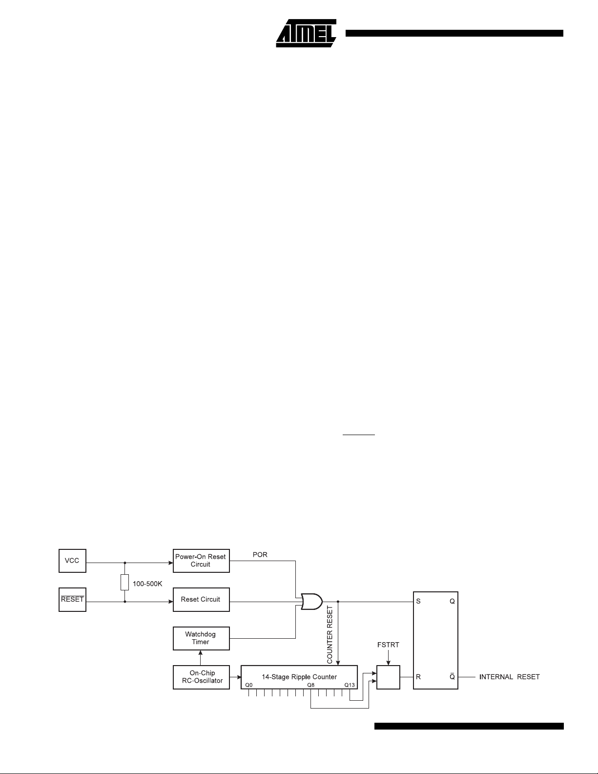
The AT90S4434/8535 has three sources of reset:
• Power-on Reset. The MCU is reset when the supply voltage is below the Power-on Reset threshold (V
POT
).
• External Reset. The MCU is reset when a low level is present on the RESET pin for more than 50 ns.
• Watchdog Reset. The MCU is reset when the Watchdog timer period expires and the Watchdog is enabled.
During reset, all I/O registers are set to their initial values and the program starts execution from address $000. The instruction placed in address $000 must be an RJMP (relative jump) instruction to the reset handling routine. If the program never
enables an interrupt source, the interrupt vectors are not used and regular program code can be placed at these locations.
The circuit diagram in Figure 23 shows the reset logic. Table 4 defines the timing and electrical parameters of the reset
circuitry.
Figure 23. Reset Logic
20
AT90S/LS4434 and AT90S/LS8535
AT90S/LS4434 and AT90S/LS8535
Table 4. Reset Characteristics (V
= 5.0V)
CC
Symbol Parameter Min Typ Max Units
(1)
V
POT
V
RST
t
TOUT
t
TOUT
Note: 1. The Power-on Reset will not work unless the supply voltage has been below V
Power-on Reset Threshold (rising) 1.0 1.4 1.8 V
Power-on Reset Threshold (falling) 0.4 0.6 0.8 V
RESET Pin Threshold Voltage 0.6 V
Reset Delay Time-out Period
FSTRT Unprogrammed
Reset Delay Time-out Period
FSTRT Programmed
11.0 16.0 21.0 ms
1.0 1.1 1.2 ms
CC
POT
(falling).
V
Table 5. Number of Watchdog Oscillator Cycles
FSTRT Time-out at VCC = 5V Number of WDT Cycles
Programmed 1.1 ms 1K
Unprogrammed 16.0 ms 16K
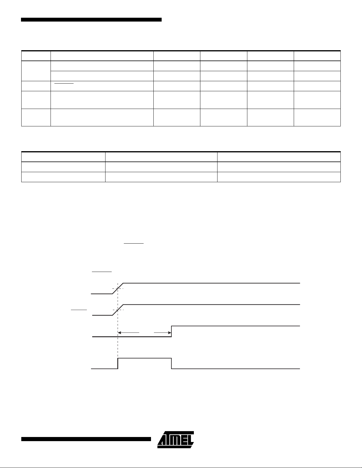
Power-on Reset
A Power-on Reset (POR) circuit ensures that the device is reset from power-on. As shown in Figure 23, an internal timer
clocked from the Watchdog Timer oscillator prevents the MCU from starting until after a certain period after V
reached the Power-on Threshold voltage (V
), regardless of the VCC rise time (see Figure 24).
POT
CC
has
The user can select the start-up time according to typical oscillator start-up time. The number of WDT oscillator cycles is
shown in Table 5. The frequency of the Watchdog oscillator is voltage-dependent as shown in “Typical Characteristics” on
page 100.
If the built-in start-up delay is sufficient, RESET
ing the pin low for a period after V
has been applied, the Power-on Reset period can be extended. Refer to Figure 25 for
CC
can be connected to VCC directly or via an external pull-up resistor. By hold-
a timing example of this.
Figure 24. MCU Start-up, RESET
VCC
RESET
TIME-OUT
INTERNAL
RESET
Tied to VCC.
V
POT
V
RST
t
TOUT
21
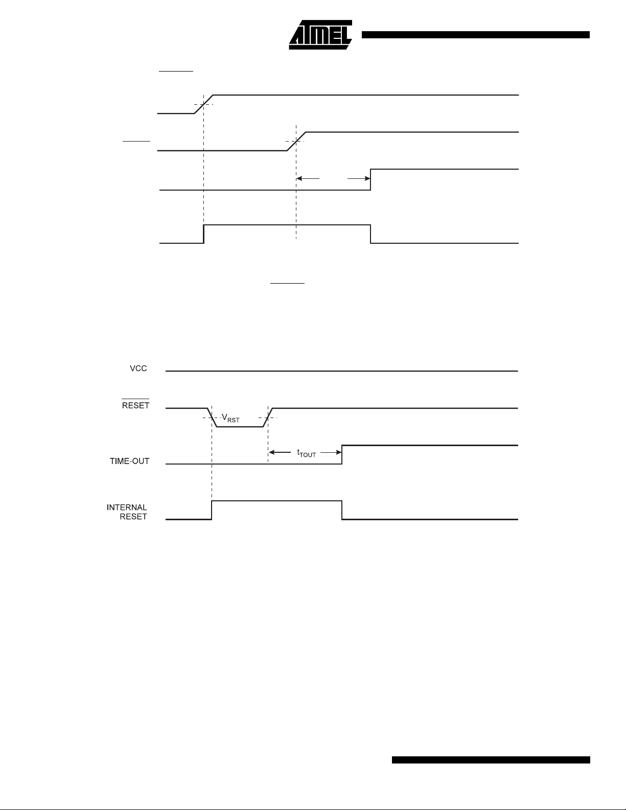
Figure 25. MCU Start-up, RESET
VCC
RESET
TIME-OUT
INTERNAL
RESET
Controlled Externally
V
POT
V
RST
t
TOUT
External Reset
An external reset is generated by a low level on the RESET
pin. Reset pulses longer than 50 ns will generate a reset, even
if the clock is not running. Shorter pulses are not guaranteed to generate a reset. When the applied signal reaches the
Reset Threshold Voltage (V
) on its positive edge, the delay timer starts the MCU after the Time-out period t
RST
TOUT
has
expired.
Figure 26. External Reset during Operation
22
AT90S/LS4434 and AT90S/LS8535
AT90S/LS4434 and AT90S/LS8535
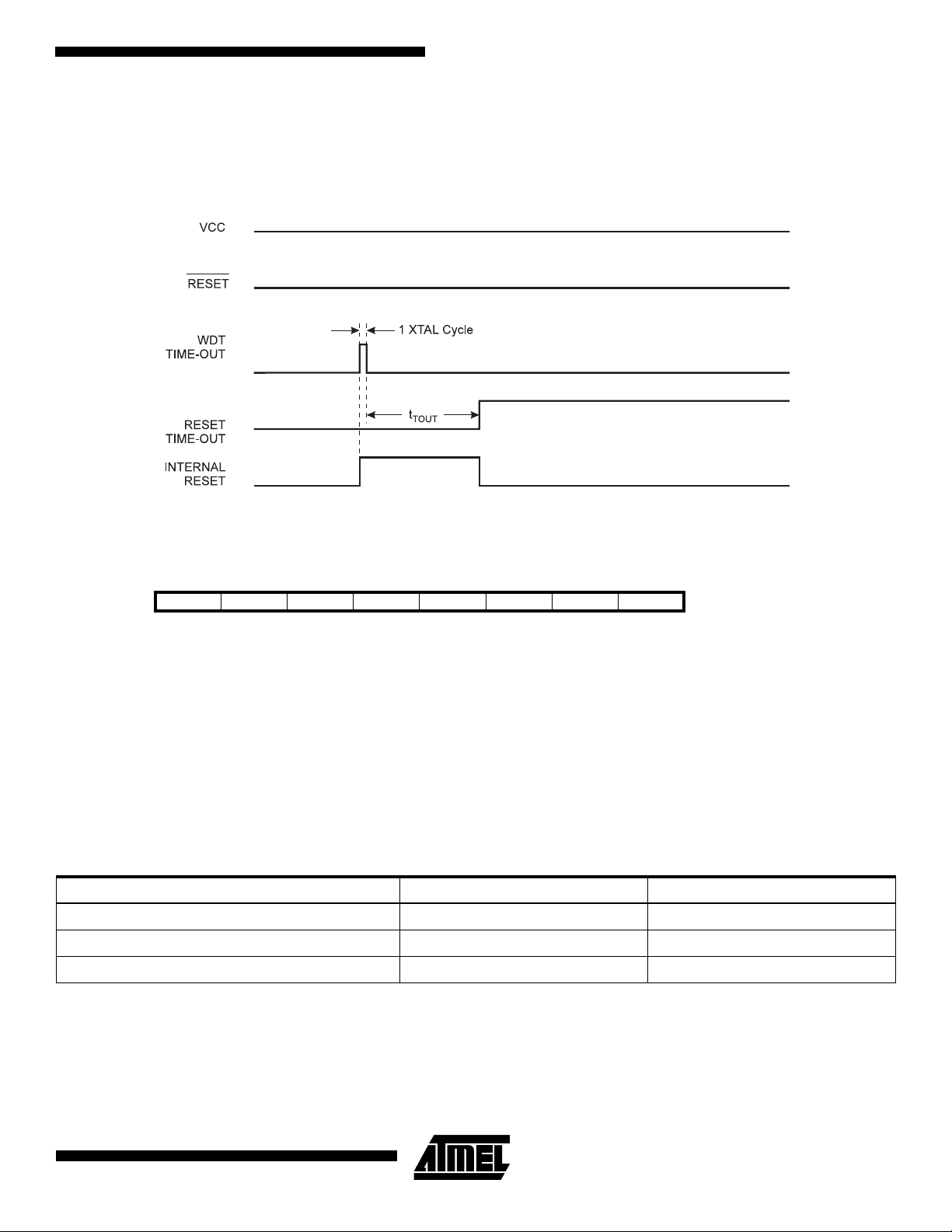
Watchdog Reset
When the Watchdog times out, it will generate a short reset pulse of 1 XTAL cycle duration. On the falling edge of this
pulse, the delay timer starts counting the Time-out period t
Figure 27. Watchdog Reset during Operation
. Refer to page 45 for details on operation of the Watchdog.
TOUT
MCU Status Register – MCUSR
The MCU Status Register provides information on which reset source caused an MCU reset.
Bit 76543210
$34 ($54) ––––––EXTRF PORF MCUSR
Read/Write R R R R R R R/W R/W
Initial value 0 0 0 0 0 0 See bit description
•
Bits 7..2 – Res: Reserved Bits
These bits are reserved bits in the AT90S4434/8535 and always read as zero.
Bit 1 – EXTRF: External Reset Flag
•
After a power-on reset, this bit is undefined (X). It can only be set by an External Reset. A Watchdog Reset will leave this bit
unchanged. The bit is reset by writing a logical “1” to the bit.
Bit 0 – PORF: Power-on Reset Flag
•
This bit is only set by a Power-on Reset. A Watchdog Reset or an External Reset will leave this bit unchanged. The bit is
reset by writing a logical “1” to the bit.
To summarize, Table 6 shows the value of these two bits after the three modes of reset.
Table 6. PORF and EXTRF Values after Reset
Reset Source EXTRF PORF
Power-on Reset undefined 1
External Reset 1 unchanged
Watchdog Reset unchanged unchanged
To make use of these bits to identify a reset condition, the user software should clear both the PORF and EXTRF bits as
early as possible in the program. Checking the PORF and EXTRF values is done before the bits are cleared. If the bit is
cleared before an External or Watchdog Reset occurs, the source of reset can be found by using Table 7.
23

Table 7. Reset Source Identification
EXTRF PORF Reset Source
0 0 Watchdog Reset
0 1 Power-on Reset
1 0 External Reset
1 1 Power-on Reset
Interrupt Handling
The AT90S4434/8535 has two 8-bit interrupt mask control registers: GIMSK (General Interrupt Mask register) and TIMSK
(Timer/Counter Interrupt Mask register).
When an interrupt occurs, the Global Interrupt Enable I-bit is cleared (zero) and all interrupts are disabled. The user software can set (one) the I-bit to enable nested interrupts. The I-bit is set (one) when a Return from Interrupt instruction (RETI)
is executed.
When the Program Counter is vectored to the actual interrupt vector in order to execute the interrupt handling routine, hardware clears the corresponding flag that generated the interrupt. Some of the interrupt flags can also be cleared by writing a
logical “1” to the flag bit position(s) to be cleared. If an interrupt condition occurs when the corresponding interrupt enable
bit is cleared (zero), the interrupt flag will be set and remembered until the interrupt is enabled or the flag is cleared by
software.
If one or more interrupt conditions occur when the global interrupt enable bit is cleared (zero), the corresponding interrupt
flag(s) will be set and remembered until the global interrupt enable bit is set (one) and will be executed by order of priority.
Note that external level interrupt does not have a flag and will only be remembered for as long as the interrupt condition is
active.
Note that the Status Register is not automatically stored when entering an interrupt routine and restored when returning
from an interrupt routine. This must be handled by software.
General Interrupt Mask Register – GIMSK
Bit 7 6 5 4 3 2 1 0
$3B ($5B) INT1 INT0 –– ––––GIMSK
Read/Write R/W R/W R R R R R R
Initial value 0 0 0 0 0 0 0 0
Bit 7 – INT1: External Interrupt Request 1 Enable
•
When the INT1 bit is set (one) and the I-bit in the Status Register (SREG) is set (one), the external pin interrupt is enabled.
The Interrupt Sense Control1 bits 1/0 (ISC11 and ISC10) in the MCU general Control Register (MCUCR) define whether
the external interrupt is activated on rising or falling edge of the INT1 pin or level sensed. Activity on the pin will cause an
interrupt request even if INT1 is configured as an output. The corresponding interrupt of External Interrupt Request 1 is
executed from program memory address $002. See also “External Interrupts.”
Bit 6 – INT0: External Interrupt Request 0 Enable
•
When the INT0 bit is set (one) and the I-bit in the Status Register (SREG) is set (one), the external pin interrupt is enabled.
The Interrupt Sense Control0 bits 1/0 (ISC01 and ISC00) in the MCU general Control Register (MCUCR) define whether
the external interrupt is activated on rising or falling edge of the INT0 pin or level sensed. Activity on the pin will cause an
interrupt request even if INT0 is configured as an output. The corresponding interrupt of External Interrupt Request 0 is
executed from program memory address $001. See also “External Interrupts.”
Bits 5.0 – Res: Reserved Bits
•
These bits are reserved bits in the AT90S4434/8535 and always read as zero.
24
AT90S/LS4434 and AT90S/LS8535

AT90S/LS4434 and AT90S/LS8535
General Interrupt Flag Register – GIFR
Bit 7 6 5 4 3 2 1 0
$3A ($5A) INTF1 INTF0 –– ––––GIFR
Read/Write R/W R/W R R R R R R
Initial value 0 0 0 0 0 0 0 0
Bit 7 – INTF1: External Interrupt Flag1
•
When an edge or logical change on the INT1 pin trigger an interrupt request, INTF1 becomes set (one). This flag is always
cleared (0) when the pin is configured for low-level interrupts, as the state of a low-level interrupt can be determined by
reading the PIN register.
If the I-bit in SREG and the INT1 bit in GIMSK are set (one), the MCU will jump to the interrupt address $002. For edge and
logic change interrupts, this flag is cleared when the interrupt routine is executed. Alternatively, the flag can be cleared by
writing a logical “1” to it.
Bit 6 – INTF0: External Interrupt Flag0
•
When an edge or logical change on the INT0 pin trigger an interrupt request, INTF0 becomes set (one). This flag is always
cleared (0) when the pin is configured for low-level interrupts, as the state of a low-level interrupt can be determined by
reading the PIN register.
If the I-bit in SREG and the INT0 bit in GIMSK are set (one), the MCU will jump to the interrupt address $001. For edge and
logic change interrupts, this flag is cleared when the interrupt routine is executed. Alternatively, the flag can be cleared by
writing a logical “1” to it.
Bits 5..0 – Res: Reserved Bits
•
These bits are reserved bits in the AT90S4434/8535 and always read as zero.
Timer/Counter Interrupt Mask Register – TIMSK
Bit 7 6 5 4 3 2 1 0
$39 ($59) OCIE2 TOIE2 TICIE1 OCIE1A OCIE1B TOIE1 – TOIE0 TIMSK
Read/Write R/W R/W R/W R/W R/W R/W R R/W
Initial value 0 0 0 0 0 0 0 0
Bit 7 – OCIE2: Timer/Counter2 Output Compare Match Interrupt Enable
•
When the OCIE2 bit is set (one) and the I-bit in the Status Register is set (one), the Timer/Counter2 Compare Match interrupt is enabled. The corresponding interrupt (at vector $003) is executed if a compare match in Timer/Counter2 occurs (i.e.,
when the OCF2 bit is set in the Timer/Counter Interrupt Flag Register [TIFR]).
Bit 6 – TOIE2: Timer/Counter2 Overflow Interrupt Enable
•
When the TOIE2 bit is set (one) and the I-bit in the Status Register is set (one), the Timer/Counter2 Overflow interrupt is
enabled. The corresponding interrupt (at vector $004) is executed if an overflow in Timer/Counter2 occurs (i.e., when the
TOV2 bit is set in the Timer/Counter Interrupt Flag Register [TIFR]).
Bit 5 – TICIE1: Timer/Counter1 Input Capture Interrupt Enable
•
When the TICIE1 bit is set (one) and the I-bit in the Status Register is set (one), the Timer/Counter1 Input Capture Event
Interrupt is enabled. The corresponding interrupt (at vector $005) is executed if a capture-triggering event occurs on pin 20,
PD6 (ICP) (i.e., when the ICF1 bit is set in the Timer/Counter Interrupt Flag Register [TIFR]).
Bit 4 – OCE1A: Timer/Counter1 Output CompareA Match Interrupt Enable
•
When the OCIE1A bit is set (one) and the I-bit in the Status Register is set (one), the Timer/Counter1 CompareA Match
interrupt is enabled. The corresponding interrupt (at vector $006) is executed if a CompareA match in Timer/Counter1
occurs (i.e., when the OCF1A bit is set in the Timer/Counter Interrupt Flag Register [TIFR]).
Bit 3 – OCIE1B: Timer/Counter1 Output CompareB Match Interrupt Enable
•
When the OCIE1B bit is set (one) and the I-bit in the Status Register is set (one), the Timer/Counter1 CompareB Match
interrupt is enabled. The corresponding interrupt (at vector $007) is executed if a CompareB match in Timer/Counter1
occurs (i.e., when the OCF1B bit is set in the Timer/Counter Interrupt Flag Register [TIFR]).
25

Bit 2 – TOIE1: Timer/Counter1 Overflow Interrupt Enable
•
When the TOIE1 bit is set (one) and the I-bit in the Status Register is set (one), the Timer/Counter1 Overflow Interrupt is
enabled. The corresponding interrupt (at vector $008) is executed if an overflow in Timer/Counter1 occurs (i.e., when the
TOV1 bit is set in the Timer/Counter Interrupt Flag Register [TIFR]).
Bit 1 – Res: Reserved Bit
•
This bit is a reserved bit in the AT90S4434/8535 and always reads zero.
Bit 0 – TOIE0: Timer/Counter0 Overflow Interrupt Enable
•
When the TOIE0 bit is set (one) and the I-bit in the Status Register is set (one), the Timer/Counter0 Overflow Interrupt is
enabled. The corresponding interrupt (at vector $009) is executed if an overflow in Timer/Counter0 occurs (i.e., when the
TOV0 bit is set in the Timer/Counter Interrupt Flag Register [TIFR]).
Timer/Counter Interrupt Flag Register – TIFR
Bit 7 6 5 4 3 2 1 0
$38 ($58) OCF2 TOV2 ICF1 OCF1A OCF1B TOV1 – TOV0 TIFR
Read/Write R/W R/W R/W R/W R/W R/W R R/W
Initial value 0 0 0 0 0 0 0 0
Bit 7 – OCF2: Output Compare Flag 2
•
The OCF2 bit is set (one) when compare match occurs between the Timer/Counter2 and the data in OCR2 (Output Compare Register2). OCF2 is cleared by hardware when executing the corresponding interrupt handling vector. Alternatively,
OCF2 is cleared by writing a logical “1” to the flag. When the I-bit in SREG and OCIE2 (Timer/Counter2 Compare Match
Interrupt Enable) and the OCF2 are set (one), the Timer/Counter2 Compare Match Interrupt is executed.
Bit 6 – TOV2: Timer/Counter2 Overflow Flag
•
The TOV2 bit is set (one) when an overflow occurs in Timer/Counter2. TOV2 is cleared by hardware when executing the
corresponding interrupt handling vector. Alternatively, TOV2 is cleared by writing a logical “1” to the flag. When the SREG
I-bit and TOIE2 (Timer/Counter2 Overflow Interrupt Enable) and TOV2 are set (one), the Timer/Counter2 Overflow Interrupt is executed. In PWM mode, this bit is set when Timer/Counter2 advances from $00.
Bit 5 – ICF1: Input Capture Flag 1
•
The ICF1 bit is set (one) to flag an input capture event, indicating that the Timer/Counter1 value has been transferred to the
Input Capture Register (ICR1). ICF1 is cleared by hardware when executing the corresponding interrupt handling vector.
Alternatively, ICF1 is cleared by writing a logical “1” to the flag. When the SREG I-bit and TICIE1 (Timer/Counter1 Input
Capture Interrupt Enable) and ICF1 are set (one), the Timer/Counter1 Capture Interrupt is executed.
Bit 4 – OCF1A: Output Compare Flag 1A
•
The OCF1A bit is set (one) when compare match occurs between the Timer/Counter1 and the data in OCR1A (Output
Compare Register 1A). OCF1A is cleared by hardware when executing the corresponding interrupt handling vector. Alternatively, OCF1A is cleared by writing a logical “1” to the flag. When the I-bit in SREG and OCIE1A (Timer/Counter1
Compare Match InterruptA Enable) and the OCF1A are set (one), the Timer/Counter1 Compare A Match Interrupt is
executed.
Bit 3 – OCF1B: Output Compare Flag 1B
•
The OCF1B bit is set (one) when compare match occurs between the Timer/Counter1 and the data in OCR1B (Output
Compare Register 1B). OCF1B is cleared by hardware when executing the corresponding interrupt handling vector. Alternatively, OCF1B is cleared by writing a logical “1” to the flag. When the I-bit in SREG and OCIE1B (Timer/Counter1
Compare Match InterruptB Enable) and the OCF1B are set (one), the Timer/Counter1 Compare Match B Interrupt is
executed.
Bit 2 – TOV1: Timer/Counter1 Overflow Flag
•
The TOV1 is set (one) when an overflow occurs in Timer/Counter1. TOV1 is cleared by hardware when executing the corresponding interrupt handling vector. Alternatively, TOV1 is cleared by writing a logical “1” to the flag. When the I-bit in
SREG and TOIE1 (Timer/Counter1 Overflow Interrupt Enable) and TOV1 are set (one), the Timer/Counter1 Overflow Interrupt is executed. In PWM mode, this bit is set when Timer/Counter1 advances from $0000.
Bit 1 – Res: Reserved Bit
•
This bit is a reserved bit in the AT90S4434/8535 and always reads zero.
26
AT90S/LS4434 and AT90S/LS8535
AT90S/LS4434 and AT90S/LS8535
Bit 0 – TOV0: Timer/Counter0 Overflow Flag
•
The bit TOV0 is set (one) when an overflow occurs in Timer/Counter0. TOV0 is cleared by hardware when executing the
corresponding interrupt handling vector. Alternatively, TOV0 is cleared by writing a logical “1” to the flag. When the SREG
I-bit and TOIE0 (Timer/Counter0 Overflow Interrupt Enable) and TOV0 are set (one), the Timer/Counter0 Overflow Interrupt is executed.
External Interrupts
The external interrupts are triggered by the INT1 and INT0 pins. Observe that, if enabled, the interrupts will trigger even if
the INT0/INT1 pins are configured as outputs. This feature provides a way of generating a software interrupt. The external
interrupts can be triggered by a falling or rising edge or a low level. This is set up as indicated in the specification for the
MCU Control Register (MCUCR). When the external interrupt is enabled and is configured as level-triggered, the interrupt
will trigger as long as the pin is held low.
The external interrupts are set up as described in the specification for the MCU Control Register (MCUCR).
Interrupt Response Time
The interrupt execution response for all the enabled AVR interrupts is four clock cycles minimum. Four clock cycles after
the interrupt flag has been set, the program vector address for the actual interrupt handling routine is executed. During this
4-clock-cycle period, the Program Counter (2 bytes) is pushed onto the stack and the Stack Pointer is decremented by 2.
The vector is normally a relative jump to the interrupt routine and this jump takes two clock cycles. If an interrupt occurs
during execution of a multi-cycle instruction, this instruction is completed before the interrupt is served.
A return from an interrupt handling routine (same as for a subroutine call routine) takes four clock cycles. During these four
clock cycles, the Program Counter (2 bytes) is popped back from the stack, the Stack Pointer is incremented by 2 and the
I-flag in SREG is set. When the AVR exits from an interrupt, it will always return to the main program and execute one more
instruction before any pending interrupt is served.
MCU Control Register – MCUCR
The MCU Control Register contains control bits for general MCU functions.
Bit 76543210
$35 ($55) – SE SM1 SM0 ISC11 ISC10 ISC01 ISC00 MCUCR
Read/Write R R/W R/W R/W R/W R/W R/W R/W
Initial value 0 0 0 0 0 0 0 0
Bit 7 – Res: Reserved Bit
•
This bit is a reserved bit in the AT90S4434/8535 and always reads zero.
Bit 6 – SE: Sleep Enable
•
The SE bit must be set (one) to make the MCU enter the Sleep Mode when the SLEEP instruction is executed. To avoid
the MCU entering the Sleep Mode unless it is the programmer’s purpose, it is recommended to set the Sleep Enable (SE)
bit just before the execution of the SLEEP instruction.
Bits 5, 4 – SM1/SM0: Sleep Mode Select Bits 1 and 0
•
These bits select between the three available sleep modes as shown in Table 8.
Table 8. Sleep Mode Select
SM1 SM0 Sleep Mode
00Idle
01Reserved
1 0 Power-down
11Power Save
27

Bits 3, 2 – ISC11, ISC10: Interrupt Sense Control 1 Bits 1 and 0
•
The External Interrupt 1 is activated by the external pin INT1 if the SREG I-flag and the corresponding interrupt mask in the
GIMSK is set. The level and edges on the external INT1 pin that activate the interrupt are defined in Table 9.
Table 9. Interrupt 1 Sense Control
ISC11 ISC10 Description
0 0 The low level of INT1 generates an interrupt request.
01Reserved
1 0 The falling edge of INT1 generates an interrupt request.
1 1 The rising edge of INT1 generates an interrupt request.
The value on the INT pin is sampled before detecting edges. If edge interrupt is selected, pulses that last longer than one
CPU clock period will generate an interrupt. Shorter pulses are not guaranteed to generate an interrupt. If low-level interrupt is selected, the low level must be held until the completion of the currently executing instruction to generate an
interrupt. If enabled, a level-triggered interrupt will generate an interrupt request as long as the pin is held low.
Bit 1, 0 – ISC01, ISC00: Interrupt Sense Control 0 Bits 1 and 0
•
The External Interrupt 0 is activated by the external pin INT0 if the SREG I-flag and the corresponding interrupt mask is set.
The level and edges on the external INT0 pin that activate the interrupt are defined in Table 10.
Table 10. Interrupt 0 Sense Control
ISC01 ISC00 Description
0 0 The low level of INT0 generates an interrupt request.
01Reserved
1 0 The falling edge of INT0 generates an interrupt request.
1 1 The rising edge of INT0 generates an interrupt request.
The value on the INT pin is sampled before detecting edges. If edge interrupt is selected, pulses that last longer than one
CPU clock period will generate an interrupt. Shorter pulses are not guaranteed to generate an interrupt. If low-level interrupt is selected, the low level must be held until the completion of the currently executing instruction to generate an
interrupt. If enabled, a level-triggered interrupt will generate an interrupt request as long as the pin is held low.
Sleep Modes
To enter any of the three sleep modes, the SE bit in MCUCR must be set (one) and a SLEEP instruction must be executed.
The SM0 and SM1 bits in the MCUCR register select which sleep mode (Idle, Power-down or Power Save) will be activated
by the SLEEP instruction. See Table 8.
If an enabled interrupt occurs while the MCU is in a sleep mode, the MCU wakes up, executes the interrupt routine and
resumes execution from the instruction following SLEEP. The contents of the register file, SRAM and I/O memory are
unaltered. If a reset occurs during Sleep Mode, the MCU wakes up and executes from the Reset vector.
Idle Mode
When the SM1/SM0 bits are set to 00, the SLEEP instruction makes the MCU enter the Idle Mode, stopping the CPU but
allowing SPI, UARTs, Analog Comparator, ADC, Timer/Counters, Watchdog and the interrupt system to continue operating. This enables the MCU to wake up from external triggered interrupts as well as internal ones like the Timer Overflow
and UART Receive Complete interrupts. If wake-up from the Analog Comparator Interrupt is not required, the Analog Comparator can be powered down by setting the ACD-bit in the Analog Comparator Control and Status Register (ACSR). This
will reduce power consumption in Idle Mode. When the MCU wakes up from Idle Mode, the CPU starts program execution
immediately.
28
AT90S/LS4434 and AT90S/LS8535

AT90S/LS4434 and AT90S/LS8535
Power-down Mode
When the SM1/SM0 bits are set to 10, the SLEEP instruction makes the MCU enter the Power-down Mode. In this mode,
the external oscillator is stopped while the external interrupts and the Watchdog (if enabled) continue operating. Only an
external reset, a Watchdog reset (if enabled) or an external level interrupt can wake up the MCU.
Note that when a level-triggered interrupt is used for wake-up from power-down, the low level must be held for a time
longer than the reset delay Time-out period t
When waking up from Power-down Mode, a delay from the wake-up condition occurs until the wake-up becomes effective.
This allows the clock to restart and become stable after having been stopped. The wake-up period is equal to the reset
period, as shown in Table 4 on page 21.
If the wake-up condition disappears before the MCU wakes up and starts to execute, e.g., a low-level on is not held long
enough, the interrupt causing the wake-up will not be executed.
Power Save Mode
When the SM1/SM0 bits are 11, the SLEEP instruction makes the MCU enter the Power Save Mode. This mode is identical
to Power-down, with one exception: If Timer/Counter2 is clocked asynchronously, i.e., the AS2 bit in ASSR is set,
Timer/Counter2 will run during sleep. In addition to the power-down wake-up sources, the device can also wake up from
either a Timer Overflow or Output Compare event from Timer/Counter2 if the corresponding Timer/Counter2 interrupt
enable bits are set in TIMSK and the global interrupt enable bit in SREG is set.
When waking up from Power Save Mode by an external interrupt, two instruction cycles are executed before the interrupt
flags are updated. When waking up by the asynchronous timer, three instruction cycles are executed before the flags are
updated. During these cycles, the processor executes instructions, but the interrupt condition is not readable and the interrupt routine has not started yet.
When waking up from Power Save Mode by an asynchronous timer interrupt, the part will wake up even if global interrupts
are disabled.
If the asynchronous timer is not clocked asynchronously, Power-down Mode is recommended instead of Power Save Mode
because the contents of the registers in the asynchronous timer should be considered undefined after wake-up in Power
Save Mode, even if AS2 is 0.
TOUT
.
29
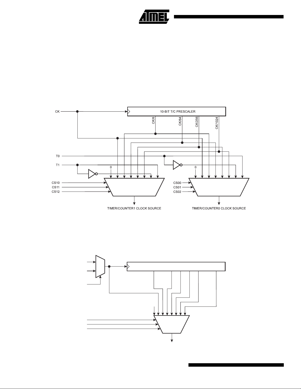
Timer/Counters
The AT90S4434/8535 provides three general-purpose Timer/Counters – two 8-bit T/Cs and one 16-bit T/C.
Timer/Counter2 can optionally be asynchronously clocked from an external oscillator. This oscillator is optimized for use
with a 32.768 kHz watch crystal, enabling use of Timer/Counter2 as a Real-time Clock (RTC). Timer/Counters 0 and 1
have individual prescaling selection from the same 10-bit prescaling timer. Timer/Counter2 has its own prescaler. These
Timer/Counters can either be used as a timer with an internal clock time base or as a counter with an external pin connection that triggers the counting.
Timer/Counter Prescalers
Figure 28. Prescaler for Timer/Counter0 and 1
TCK1
TCK0
For Timer/Counters 0 and 1, the four different prescaled selections are: CK/8, CK/64, CK/256 and CK/1024, where CK is
the oscillator clock. For the two Timer/Counters 0 and 1, CK, external source and stop can also be selected as clock
sources.
Figure 29. Timer/Counter2 Prescaler
CK
TOSC1
AS2
CS20
CS21
CS22
PCK2
10-BIT T/C PRESCALER
PCK2/8
0
TIMER/COUNTER2 CLOCK SOURCE
PCK2
PCK2/32
PCK2/64
PCK2/128
PCK2/256
PCK2/1024
30
AT90S/LS4434 and AT90S/LS8535
 Loading...