

Atmel AVR AT90S2333, AVR AT90LS2333, AVR AT90LS4433, AVR AT90S4433 User Manual

Features
• High-performance and Low-power AVR
– 118 Powerful Instructions - Most Single Cycle Execution
– 32 x 8 General Purpose Working Registers
– Up to 8 MIPS Throughput at 8 MHz
• Data and Nonvolatile Program Memory
– 2K/4K Bytes of In-System Programmable Flash
Endurance 1,000 Write/Erase Cycles
– 128 Bytes of SRAM
– 128/256 Bytes of In-System Programmable EEPROM
Endurance: 100,000 Write/Erase Cycles
– Programming Lock for Flash Program and EEPROM Data Security
• Peripheral Features
– One 8-bit Timer/Counter with Separate Prescaler
– Expanded 16-bit Timer/Counter with Separate Prescaler,
Compare, Capture Modes and 8-, 9- or 10-bit PWM
– On-chip Analog Comparator
– Programmable Watchdog Timer with Separate On-chip Oscillator
– Programmable UART
– 6-channel, 10-bit ADC
– Master/Slave SPI Serial Interface
• Special Microcontroller Features
– Brown-Out Reset Circuit
– Enhanced Power-on Reset Circuit
– Low-Power Idle and Power Down Modes
– External and Internal Interrupt Sources
• Specifications
– Low-power, High-speed CMOS Process Technology
– Fully Static Operation
• Power Consumption at 4 MHz, 3V, 25°C
– Active: 3.4 mA
– Idle Mode: 1.4 mA
– Power Down Mode: <1 µA
• I/O and Packages
– 20 Programmable I/O Lines
– 28-pin PDIP and 32-pin TQFP
• Operating Voltage
– 2.7V - 6.0V (AT90LS2333 and AT90LS4433)
– 4.0V - 6.0V (AT90S2333 and AT90S4433)
• Speed Grades
– 0 - 4 MHz (AT90LS2333 and AT90LS4433)
– 0 - 8 MHz (AT90S2333 and AT90S4433)
®
8-bit RISC Architecture
8-bit
Microcontroller
with 2K/4K bytes
In-System
Programmable
Flash
AT90S2333
AT90LS2333
AT90S4433
AT90LS4433
Preliminary
Pin Configurations
TQFP Top View PDIP
PD2 (INT0)
PD1 (TXD)
PD0 (RDX)
RESET
PC5 (ADC5)
PC4 (ADC4)
PC3 (ADC3)
PC2 (ADC2)
(INT1) PD3
(T0) PD4
VCC
GND
XTAL1
XTAL2
32313029282726
1
2
3
NC
4
5
6
NC
7
8
9101112131415
(T1) PD5
(AIN0) PD6
(AIN1) PD7
(SS) PB2
(ICP) PB0
(OC1) PB1
25
16
(MOS1) PB3
(MOS0) PB4
24
23
22
21
20
19
18
17
PC1 (ADC1)
PC0 (ADC0)
NC
AGND
AREF
NC
AVCC
PB5 (SCK)
RESET
(RXD) PD0
(TXD) PD1
(INT0) PD2
(INT1) PD3
(T0) PD4
VCC
GND
XTAL1
XTAL2
(T1) PD5
(AIN0) PD6
(AIN1) PD7
(ICP) PB0
1
2
3
4
5
6
7
8
9
10
11
12
13
14
28
27
26
25
24
23
22
21
20
19
18
17
16
15
PC5 (ADC5)
PC4 (ADC4)
PC3 (ADC3)
PC2 (ADC2)
PC1 (ADC1)
PC0 (ADC0)
AGND
AREF
AVCC
PB5 (SCK)
PB4 (MISO)
PB3 (MOSI)
PB2 (SS)
PB1 (OC1)
Rev. 1042D–04/99
1

Description
The AT90S2333/4433 is a low-power CMOS 8-bit microcontroller based on the AVR RISC architecture. By executing powerful instructions in a single clock cycle, the AT90S2333/4433 achieves throughputs approaching 1 MIPS per MHz allowing
the system designer to optimize power consumption versus processing speed.
The AVR core combines a rich instruction set with 32 general purpose working registers. All the 32 registers are directly
connected to the Arithmetic Logic Unit (ALU), allowing two independent registers to be accessed in one single instruction
executed in one clock cycle. The resulting architecture is more code efficient while achieving throughputs up to ten times
faster than conventional CISC microcontrollers.
The AT90S2333/4433 provides the following features: 2K/4K bytes of In-System Programmable Flash, 128/256 bytes
EEPROM, 128 bytes SRAM, 20 general purpose I/O lines, 32 general purpose working registers, two flexible
timer/counters with compare modes, internal and external interrupts, a programmable serial UART, 6-channel, 10-bit ADC,
programmable Watchdog Timer with internal oscillator, an SPI serial port and two software selectable power saving modes.
The Idle mode stops the CPU while allowing the SRAM, timer/counters, SPI port and interrupt system to continue functioning. The Power Down mode saves the register contents but freezes the oscillator, disabling all other chip functions until the
next interrupt or hardware reset.
The device is manufactured using Atmel’s hig h-density nonvolatile me mory technol ogy. The on-chi p Flash program memory can be reprogrammed in-system through an SPI serial interface or by a conventional nonvolatile memory programmer.
By combining a RISC 8-bit CPU with In-System Programmable Flash on a monolithic chip, the Atmel AT90S2333/4433 is a
powerful microcontroller that provides a highly flexible and cost effective solution to many embedded control applications.
The AT90S2333/4433 AVR is s uppo rt ed with a ful l s uit e of prog ra m and syste m de vel op men t tool s i nclud ing : C compilers,
macro assemblers, program debugger/simulators, in-circuit emulators, and evaluation kits.
Table 1. Comparison Table
Device Flash EEPROM SRAM Voltage Range Frequency
AT90S2333 2K 128B 128B 4.0V - 6.0V 0 - 8 MHz
AT90LS2333 2K 128B 128B 2.7V - 6.0V 0 - 4 MHz
AT90S4433 4K 256B 128B 4.0V - 6.0V 0 - 8 MHz
AT90LS4433 4K 256B 128B 2.7V - 6.0V 0 - 4 MHz
2
AT90S/LS2333 and AT90S/LS4433
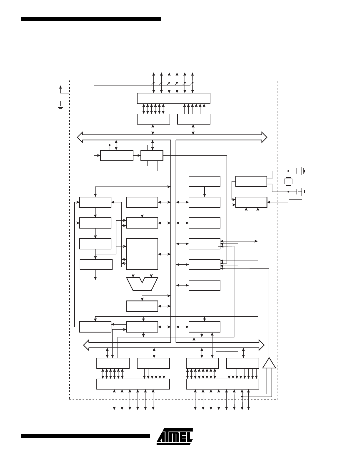
Block Diagram
Figure 1. The AT90S2333/4433 Block Diagram
VCC
AT90S/LS2333 and AT90S/LS4433
PC0 - PC5
PORTC DRIVERS
GND
AVCC
AGND
AREF
PROGRAM
COUNTER
PROGRAM
FLASH
INSTRUCTION
REGISTER
INSTRUCTION
DECODER
CONTROL
LINES
DATA REGISTER
PORTC
ANALOG MUX ADC
STACK
POINTER
SRAM
GENERAL
PURPOSE
REGISTERS
X
Y
Z
ALU
REG. PORTC
8-BIT DATA BUS
DATA DIR.
INTERNAL
OSCILLATOR
WATCHDOG
TIMER
MCU CONTROL
REGISTER
TIMER/
COUNTERS
INTERRUPT
UNIT
EEPROM
OSCILLATOR
TIMING AND
CONTROL
XTAL1
XTAL2
RESET
PROGRAMMING
LOGIC
DATA REGISTER
PORTB
PORTB DRIVERS
STATUS
REGISTER
PB0 - PB5
SPI
DATA DIR.
REG. PORTB
UART
DATA REGISTER
PORTD
PORTD DRIVERS
PD0 - PD7
DATA DIR.
REG. PORTD
+
COMPARATOR
ANALOG
3

Pin Descriptions
VCC
Supply voltage
GND
Ground
Port B (PB5..PB0)
Port B is a 6-bit bi-directional I/O port with internal pullup resistors. The Port B output buffers can sink 20 mA. As inputs,
Port B pins that are externally pulled low will source current if the pull-up resistors are activated.
Port B also serves the functions of various special features of the AT90S2333/4433 as listed on page 60.
The port B pins are tristated when a reset condition becomes active, even if the clock is not running.
Port C (PC5..PC0)
Port C is a 6-bit bi-directional I/O port with internal pullup resistors. The Port C output buffers can sink 20 mA. As inputs,
Port C pins that are ex ter na lly pul le d l ow wi ll s our ce c ur rent if the pull-up resistor s ar e a ctiv ated . P or t C a lso s er ves as the
analog inputs to the A/D Converter.
The port C pins are tristated when a reset condition becomes active, even if the clock is not running.
Port D (PD7..PD0)
Port D is an 8-bit bi-di r ectio nal I/O port with internal pull-up resi st or s. The P or t D ou tput buff er s can si nk 20 m A. A s inp uts ,
Port D pins that are externally pulled low will source current if the pull-up resistors are activated.
Port D also serves the functions of various special features of the AT90S2333/4433 as listed on page 67.
The port D pins are tristated when a reset condition becomes active, even if the clock is not running.
RESET
Reset input. An exter nal res et is gen erate d by a lo w le vel on the RESET pin. Res et p ul ses l on ger th an 5 0 n s w ill g ener a te
a reset, even if the clock is not running. Shorter pulses are not guaranteed to generate a reset.
XTAL1
Input to the inverting oscillator amplifier and input to the internal clock operating circuit.
XTAL2
Output from the inverting oscillator amplifier
AVCC
This is the supply volt age pin for the A/D Conv erter. It should be ext ernally conn ected to V
page 52 for details on operation of the ADC.
AREF
This is the analog reference input for the A/D Converter. For ADC operations, a voltage in the range 2.7V to AVCC must be
applied to this pin.
AGND
If the board has a separate ana log ground plane, this pin should be con nec ted to thi s gro und pla ne. Ot he rwis e, c onn ec t to
GND.
via a low-pass filter. Se e
CC
4
AT90S/LS2333 and AT90S/LS4433
AT90S/LS2333 and AT90S/LS4433
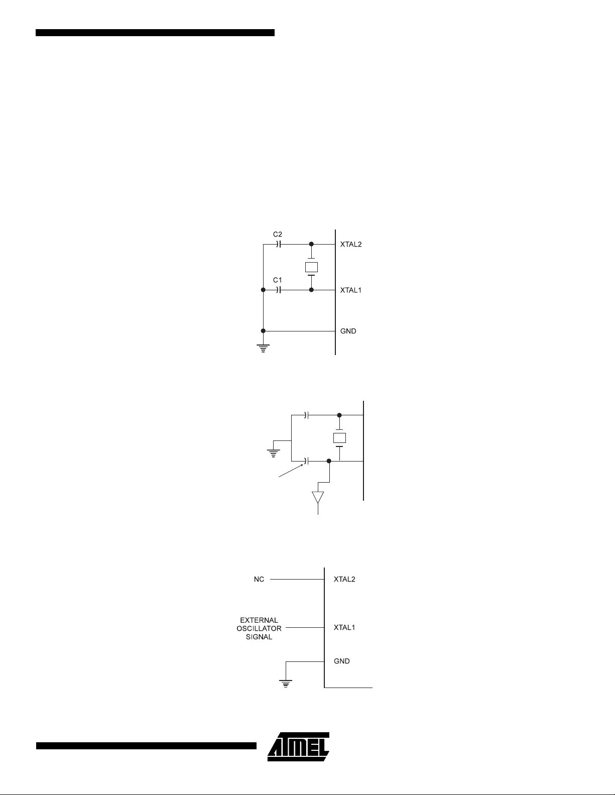
Clock Options
Crystal Oscillator
XTAL1 and XTAL2 are input and output, respectively, of an inverting amplifier which can be configured for use as an onchip oscillator, as shown in Figure 2 and Figure 3. Either a quartz crystal or a ceramic resonator may be used.
External Clock
If the oscillator is to be used as a clock for an external device, the clock signal from XTAL2 may be routed to one HC buffer,
while reducing the load capacitor by 5 pF, as shown in Figure 3. To drive the device from an external clock source, XTAL2
should be left unconnected while XTAL1 is driven as shown in Figure 4.
Figure 2. Oscillator Conn ec tion s
Figure 3. Using MCU Oscillator as a Clock for an External Device
REDUCE BY 5
F
P
HC
MAX 1 HC BUFFER
Figure 4. External Clock Drive Configuration
XTAL1
XTAL2
5
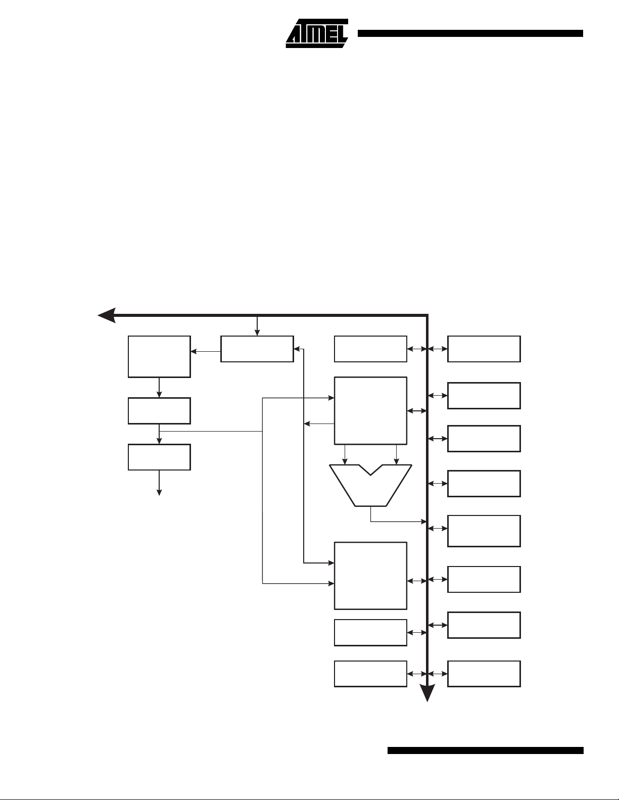
Architectural Overview
The fast-access register file concept contains 32 x 8-bit general purpose working registers with a single clock cycle access
time. This means th at d ur ing one single clock cycle , on e A r ith meti c Log ic Uni t (A LU) op er ati on is ex ec ute d. Two ope ra nds
are output from the register file, the operation is executed, and the result is stored back in the register file - in one clock
cycle.
Six of the 32 registers can be used as three 16-bits indirect address register pointers for Data Space addressing - enabling
efficient address cal culation s. O ne of the three address point ers is also used a s the ad dress pointer for the c onst ant tabl e
look up function. These added function registers are the 16-bits X-register, Y-register and Z-register.
The ALU supports arithmetic and logic functions between registers or between a constant and a register. Single register
operations are also executed in the ALU. Figure 5 shows the AT90S2333/4433 AVR RISC microcontroller architecture.
In addition to the register operation, the conventional memory addressing modes can be used on the register file as well.
This is enabled by the fa ct th at the regis ter file is as signe d the 32 lowerm ost Data S pace a ddre sses ($00 - $1F) , al lowin g
them to be accessed as though they were ordinary memory locations.
Figure 5. The AT90S2333/4433 AVR RISC Architecture
AVR
1K/2K X 16
Program
Memory
Instruction
Register
Instruction
Decoder
Control Lines
AT90S2333/4433 Architecture
Data Bus 8-bit
Program
Counter
Direct Addressing
Indirect Addressing
Status
and Control
32 x 8
General
Purpose
Registrers
ALU
128 x 8
Data
SRAM
Interrupt
Unit
SPI
Unit
Serial
UART
8-bit
Timer/Counter
16-bit
Timer/Counter
with PWM
Watchdog
Timer
128/256 x 8
EEPROM
20
I/O Lines
6
AT90S/LS2333 and AT90S/LS4433
Analog to Digital
Converter
Analog
Comparator

AT90S/LS2333 and AT90S/LS4433
The I/O memory space contains 64 addresses for CPU peripheral functions a s Control Registers, Timer/Counters, A/Dconverters, and other I/O functions. The I/O Memory can be accessed directly, or as the Data Space locations following
those of the register file, $20 - $5F.
The AVR uses a Harvard architecture concept - with separate memories and buses for program and data. The program
memory is executed with a two stage pipeline. While one instruction is being executed, the next instruction is pre-fetched
from the program memory. This concept enables instructions to be executed in every clock cycle.
The program memory is In-System Programmable Flash memory.
With the relativ e jump an d call i nstru ctions , the whol e 1K/2K word a ddress space is di rect ly acces sed. Mo st AVR i nstru c-
tions have a single 16-bit word format. Every program memory address contains a 16- or 32-bit instruction.
During interrupts and su broutine ca lls, the retu rn addr ess program counte r (P C) is s tored on the stack. The st ack is effec-
tively alloca ted in the ge neral da ta SRAM, an d conseq uently th e stack size is onl y limite d by the total SRAM size and the
usage of the SRAM. All use r progr ams must in itial ize the SP in the re set routi ne (bef ore su broutine s or inter rupts ar e executed). The 8-bit stack pointer SP is read/write accessible in the I/O space.
The 128 bytes data SRAM can be easily accessed through the five different addressing modes supported in the AVR
architecture.
The memory spaces in the AVR architecture are all linear and regular memory maps.
Figure 6. AT90S2333/4433 Memory Maps
Data MemoryProgram Memory
Program Flash
(1K/2K x 16)
$000
32 Gen. Purpose
Working Registers
64 I/O Registers
Internal SRAM
(128 x 8)
$0000
$001F
$0020
$005F
$0060
$00DF
$3FF/ $7FF
A flexible interrupt module has its control registers in the I/O space with an additional global interrupt enable bit in the status
register. All the different interrup ts have a sepa rate inter rupt vecto r in the interrupt ve ctor tab le at the beginn ing of the program memory. The different int errupts have pr iority in acco rdance with thei r interrupt vec tor position . The lower the
interrupt vector address, the higher the priority.
7
General Purpose Register File
Figure 7 shows the structure of the 32 general purpose working registers in the CPU.
Figure 7. AVR CPU General Purpose Working Registers
70Addr.
R0 $00
R1 $01
R2 $02
…
R13 $0D
General R14 $0E
Purpose R15 $0F
Working R16 $10
Registers R17 $11
…
R26 $1A X-register low byte
R27 $1 B X-register high byte
R28 $1C Y-register low byte
R29 $1D Y-register high byte
R30 $1E Z-register low byte
R31 $1F Z-register high byte
All the register opera ting instructi ons in the instructio n set have direct and single cycle access to all registe rs. The only
exceptions are the five constant arithmetic and logic instructions SBCI, SUBI, CPI, ANDI, and ORI between a constant and
a register, and the LDI ins truc ti on for load i mm edi ate c on sta nt da ta. The se instr uct io ns appl y to the second half of the registers in the register file - R16..R31. The general SBC, SUB, CP, AND, and OR, and all other operations between two
registers or on a single register apply to the entire register file.
As shown in Figu re 7, each regi ster is als o as signe d a da ta mem ory addre ss, mappin g them dire ctly into the fi rst 32 locations of the user Data Space. Although not being physicall y implemented as SRAM locations, this memory or ganization
provides great flexibility in access of the registers, as the X, Y and Z registers can be set to index any register in the file.
X-register, Y-register, and Z-register
The registers R26..R 31 ha ve some a dded funct ions to th eir general pur pose us age. These regis ters a re a ddress poi nters
for indirect addressing of the Data Space. The three indirect address registers X, Y and Z are defined as:
Figure 8. X, Y and Z Registers
15 0
X - register 7 0 7 0
R27 ($1B) R26 ($1A)
15 0
Y - register 7 0 7 0
R29 ($1D) R28 ($1C)
15 0
Z - register 7 0 7 0
R31 ($1F) R30 ($1E)
In the different address ing mod es , thes e ad dr ess r egi st ers h ave func ti ons as fix ed di spla cement, automatic increm ent an d
decrement (see the descriptions for the different instructions).
8
AT90S/LS2333 and AT90S/LS4433
AT90S/LS2333 and AT90S/LS4433
ALU - Arithmetic Logic Unit
The high-performance AVR ALU operates in direct connection with all the 32 general purpose working registers. Within a
single clock cy cl e, AL U operations between r egis ter s in the re gis te r f il e ar e exec uted . The ALU operations are div i ded in to
three main categories - arithmetic, logical, and bit-functions.
In-System Programmable Flash Program Memory
The AT90S2333/4433 contains 2K/4K bytes on-chip In-System Programmable Flash memory for program storage. Since
all instructions are 16-or 32-bit words, the Flash is organized as 1K/2K x 16. The Flash memory has an endurance of at
least 1000 write/erase cycles. The AT90S2333/4433 Program Counter (PC) is 10/11 bits wide, thus addressing the
1024/2048 progr am memo ry addr esses. See page 78 for a deta iled de scrip tion on Fl ash data dow nloadi ng. See page 10
for the different program memory addressing modes.
Figure 9. SRAM Organization
Register File Data Address Space
R0 $0000
R1 $0001
R2 $0002
……
R29 $001D
R30 $001E
R31 $001F
I/O Registers
$00 $0020
$01 $0021
$02 $0022
……
$3D $005D
$3E $005E
$3F $005F
Internal SRAM
$0060
$0061
…
$00DE
$00DF
SRAM Data Memory
The figure above shows how the AT90S2333/4433 SRAM Memory is organized.
The lower 224 Data Memory locations add ress the Regi ster file, the I/O Memo ry and the intern al data SRAM. The fir st 96
locations address the Register File and I/O Memory, and the next 128 locations address the internal data SRAM.
The five different addressing modes for the data memory cover: Direct, Indirect with Displacement, Indirect, Indirect with
Pre-Decrement, and Ind irect wit h Post-In crement . In the reg ister fil e, regis ters R26 to R31 featur e the indir ect add ressing
pointer registers.
The direct addressing reaches the entire data space. The Indirect with Displacement mode features a 63 address locations
reach from the base address given by the Y or Z-register.
When using register indirect addressing modes with automatic pre-decrement and post-increment, the address registers X,
Y and Z are decremented and incremented.
9
The 32 general purpose working registers, 64 I/O registers and the 128 bytes of internal data SRAM in the
AT90S2333/4433 are all accessible through all these addressing modes.
See the next section for a detailed description of the different addressing modes.
Program and Data Addressing Modes
The AT90S2333/4433 AVR RISC microcontroller supports powerful and efficient addressing modes for access to the Flash
program memory, SRAM , Reg is ter File, a nd I/O data memory. This sec tio n de sc r ib es the different addressing modes s upported by the AVR architecture. In the figures, OP means the operation code part of the instruction word. To simplify, not all
figures show the exact location of the addressing bits.
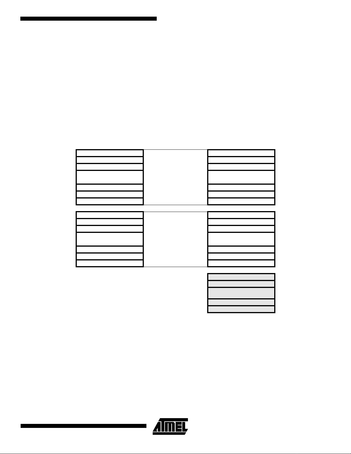
Register Direct, Single Register Rd
Figure 10. Direct Single Register Addressing
The operand is contained in register d (Rd).
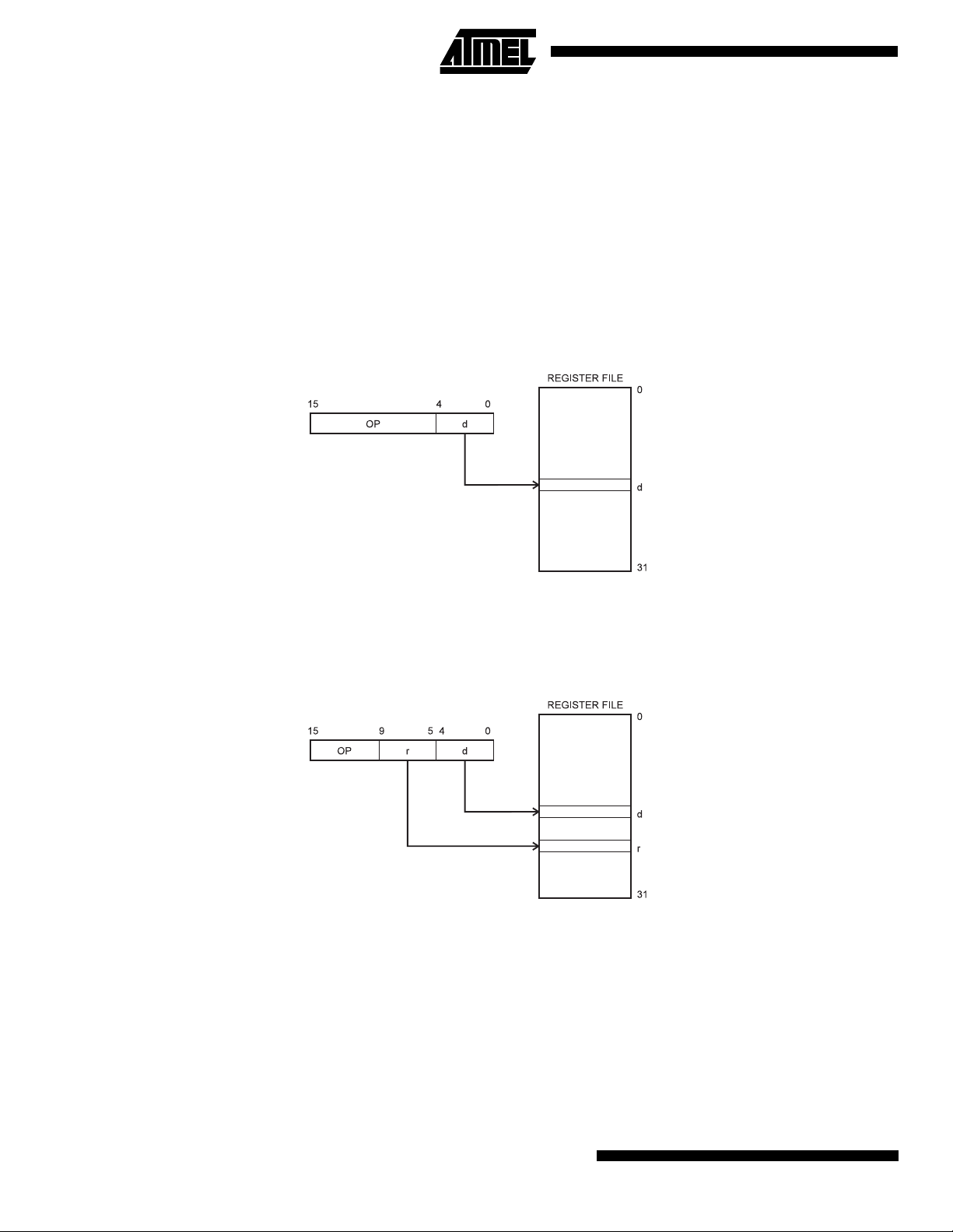
Register Direct, Two Registers Rd and Rr
Figure 11. Direct Register Addressing, Two Registers
Operands are contained in register r (Rr) and d (Rd). The result is stored in register d (Rd).
10
AT90S/LS2333 and AT90S/LS4433
AT90S/LS2333 and AT90S/LS4433
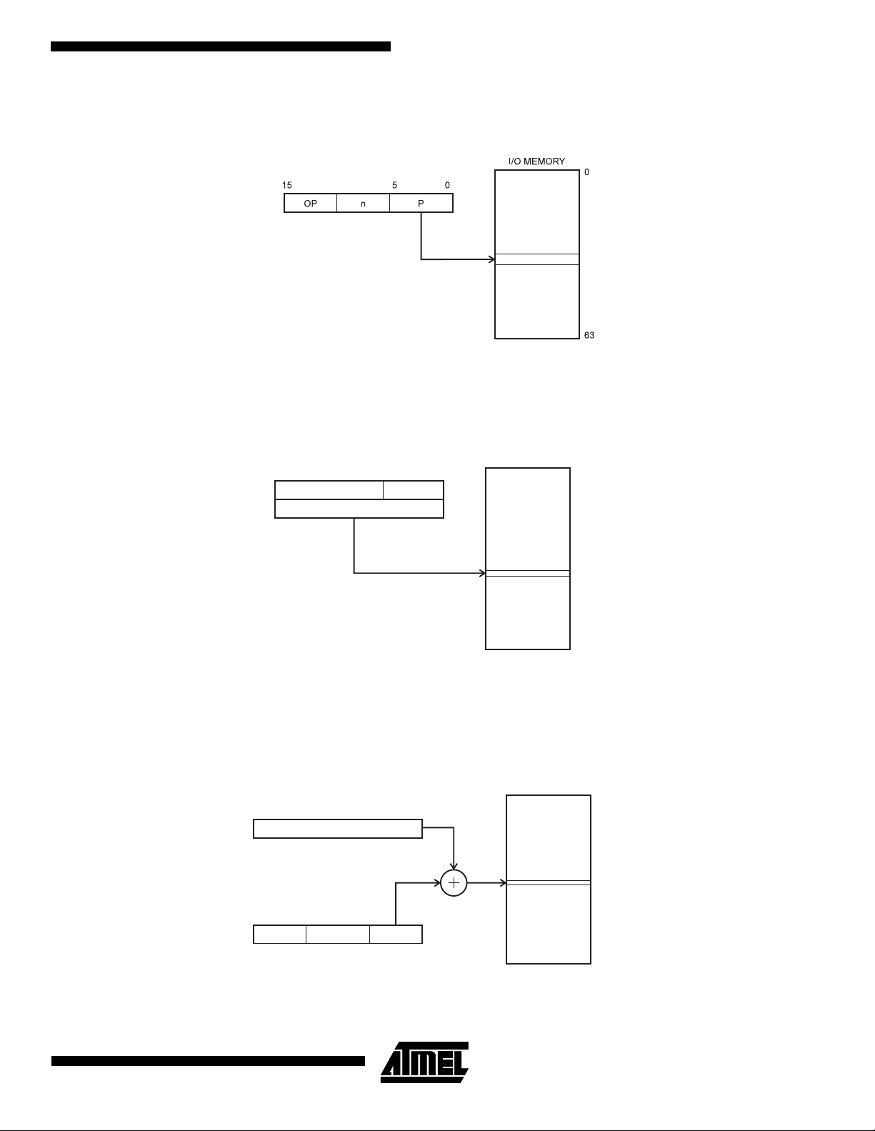
I/O Direct
Figure 12. I/O Direct Addressing
Operand address is contained in 6 bits of the instruction word. n is the destination or source register address.
Data Direct
Figure 13. Direct Data Addressing
31
OP Rr/Rd
15 0
20 19
16 LSBs
Data Space
16
$0000
$00DF
A 16-bit Data Address is contained in the 1 6 LSBs of a two-word instruction. Rd/Rr s pecify the destination or source
register.
Data Indirect with Displacement Figure 14. Data Indirect with Displacement
15
Y OR Z - REGISTER
15
OP an
Data Space
0
05610
$0000
$00DF
Operand address is the re sult of the Y or Z-register contents added to the address contained in 6 bits of the in struction
word.
11
Data Indirect
Figure 15. Data Indirect Addressing
015
X, Y, OR Z - REGISTER
Operand address is the contents of the X, Y, or the Z-register.
Data Indirect with Pre-Decrement
Figure 16. Data Indirect Addressing with Pre-Decrement
015
X, Y, OR Z - REGISTER
Data Space
Data Space
$0000
$00DF
$0000
-1
$00DF
The X, Y, or the Z-register is decremented before the operation. Operand address is the decremented contents of the X, Y,
or the Z-register.
Data Indirect with Post-Increment
Figure 17. Data Indirect Addressing with Post-Increment
Data Space
015
X, Y, OR Z - REGISTER
1
$0000
$00DF
The X, Y, or the Z-register is inc r em ente d afte r th e ope ratio n. O perand address is the content of the X , Y, o r th e Z-reg ister
prior to incrementing.
12
AT90S/LS2333 and AT90S/LS4433

AT90S/LS2333 and AT90S/LS4433
Constant Addressing Using the LPM Instruction
Figure 18. Code Memory Constant Addressing
PROGRAM MEMORY
Constant byte address is specified by the Z-register contents. The 15 MSBs select word address (0 - 1K/2K), the LSB
selects low byte if cleared (LSB = 0) or high byte if set (LSB = 1).
Indirect Program Addressing, IJMP and ICALL
Figure 19. Indirect Program Memory Addressing
PROGRAM MEMORY
$000
$3FF/$7FF
$000
$3FF/$7FF
Program execution continues at address contained by the Z-register (i.e. the PC is loaded with the contents of the Zregister).
Relative Program Addressing, RJMP and RCALL
Figure 20. Relative Program Memory Addressing
PROGRAM MEMORY
$000
$3FF/$7FF
Program execution continues at address PC + k + 1. The relative address k is from -2048 to 2047.
13
EEPROM Data Memory
The AT90S2333/4433 contains 128/256 bytes of data EEPROM memory. It is organized as a separate data space, in
which single bytes can be read and written. The EEPROM has an e ndurance of at least 1 00,000 write/erase cy cles per
location. The access between the EEPROM and the CPU is described on page 44 specifying the EEPROM address registers, the EEPROM data register, and the EEPROM control register.
For the SPI data download ing, s ee page 78 for a detai led de script ion. The EEPRO M data memory is In-S ystem Progr am-
mable through the SPI port. Please refer to the “EEPRO M Read/Write Access” section on p age 38 for a thorough
description on EEPROM access.
Memory Access Times and Instruction Execution Timing
This section describes the general access timing concepts for instruction execution and internal memory access.
The AVR CPU is driven b y the S yste m Clock Ø, di rectly gener ated from the ex ternal c lock c rystal for the c hip. No interna l
clock division is used.
Figure 21 shows the parallel instructio n fetches and instructio n executions enabl ed by the Harvard architec ture and the
fast-access register file concept. This is the basic pipelining concept to obtain up to 1 MIPS per MHz with the corresponding
unique results for functions per cost, functions per clocks, and functions per power-unit.
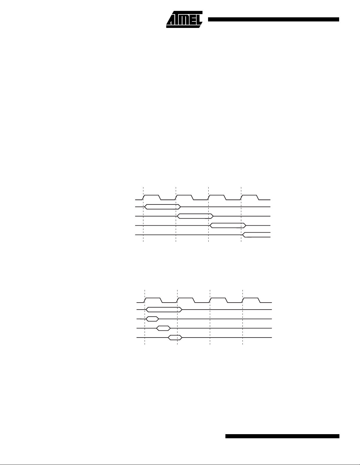
Figure 21. The Parallel Instruction Fetches and Instruction Executions
T1 T2 T3 T4
System Clock Ø
1st Instruction Fetch
1st Instruction Execute
2nd Instruction Fetch
2nd Instruction Execute
3rd Instruction Fetch
3rd Instruction Execute
4th Instruction Fetch
Figure 22 shows the internal timing concept for the register file. In a single clock cycle an ALU operation using two register
operands is executed, and the result is stored back to the destination register.
Figure 22. Single Cycle ALU Operation
T1 T2 T3 T4
System Clock Ø
Total Execution Time
Register Operands Fetch
ALU Operation Execute
Result Write Back
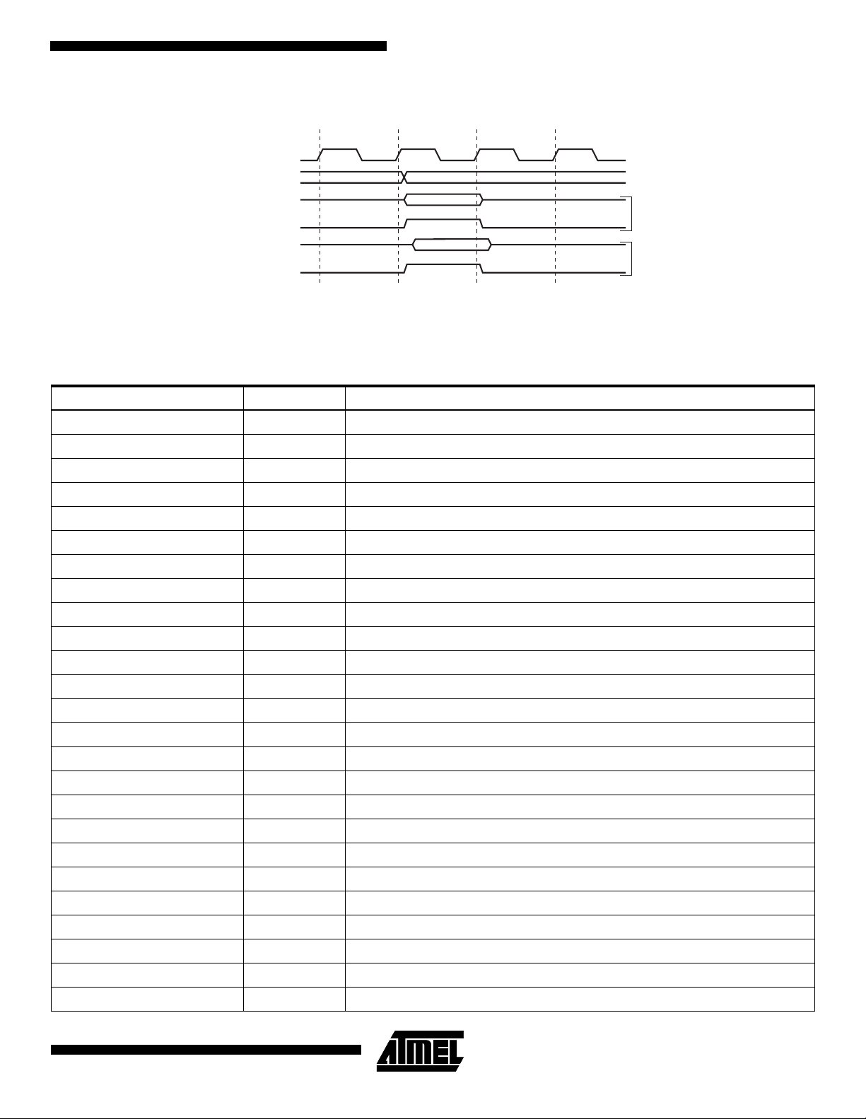
The internal data SRAM access is performed in two System Clock cycles as described in Figure 23.
14
AT90S/LS2333 and AT90S/LS4433
AT90S/LS2333 and AT90S/LS4433
Figure 23. On-Chip Data SRAM Access Cycles
T1 T2 T3 T4
System Clock Ø
Address
Data
WR
Data
RD
Prev. Address
I/O Memory
The I/O space definition of the AT90S2333/4433 is shown in the following table:
Table 2. AT90S2333/4433 I/O Space
I/O Address (SRAM Address) Name Function
$3F ($5F) SREG Status REGister
$3D ($5D) SP Stack Pointer
$3B ($5B) GIMSK General Interrupt MaSK register
Address
Read Write
$3A ($5A) GIFR General Interrupt Flag Register
$39 ($59) TIMSK Timer/Counter Interrupt MaSK register
$38 ($58) TIFR Timer/Counter Interrupt Flag register
$35 ($55) MCUCR MCU general Control Register
$34 ($54) MCUSR MCU general Status Register
$33 ($53) TCCR0 Timer/Counter0 Control Register
$32 ($52) TCNT0 Timer/Counter0 (8-bit)
$2F ($4F) TCCR1A Timer/Counter1 Control Register A
$2E ($4E) TCCR1 B Timer/Counter1 Control Register B
$2D ($4D) TCNT1H Timer/Counter1 High Byte
$2C ($4C) TCNT1L Timer/Counter1 Low Byte
$2B ($4B) OCR1H Timer/Counter1 Output Compare Register High Byte
$2A ($4A) OCR1L Timer/Counter1 Output Compare Register Low Byte
$27 ($47) ICR1H Timer/Counter1 Input Capture Register High Byte
$26 ($46) ICR1L Timer/Counter 1 Input Capture Register Low Byte
$21 ($41) WDTCR Watchdog Timer Control Register
$1E ($3E) EEAR EEPROM Address Register
$1D ($3D) EEDR EEPROM Data Register
$1C ($3C) EECR EEPROM Control Register
$18 ($38) PORTB Data Register, Port B
$17 ($37) DDRB Data Direction Register, Port B
$16 ($36) PINB Input Pins, Port B
15

Table 2. AT90S2333/4433 I/O Space (Continued)
I/O Address (SRAM Address) Name Function
$15 ($35) PORTC Data Register, Port C
$14 ($34) DDRC Data Direction Register, Port C
$13 ($33) PINC Input Pins, Port C
$12 ($32) PORTD Data Register, Port D
$11 ($31) DDRD Data Direction Register, Port D
$10 ($30) PIND Input Pins, Port D
$0F ($2F) SPDR SPI I/O Data Register
$0E ($2E) SPSR SPI Status Register
$0D ($2D) SPCR SPI Control Register
$0C ($2C) UDR UART I/O Data Register
$0B ($2B) USR UART Status Register
$0A ($2A) UCR UART Co ntro l Regis ter
$09 ($29) UBRR UART Baud Rate Register
$08 ($28) ACSR Analog Comparator Control and Status Register
$07 ($27) ADMUX ADC Multiplexer Select Register
$06 ($26) ADCSR ADC Control and Status Register
$05 ($25) ADCH ADC Data Register High
$04 ($24) ADCL ADC Data Register Low
$03 ($23) UBRRHI UART Baud Rate Register High
Note: Reserved and unused locations are not shown in the table.
All AT90S2333/4433 I/Os and per ipheral s are plac ed in th e I/O space . The I/O lo catio ns are acces sed by the IN and OU T
instructions trans ferr ing d ata be tween th e 32 general purpose working registers and t he I/O s pa ce . I/ O r egi st ers within the
address range $00 - $1F are directly bit-a ccessibl e using the SBI and CBI instruct ions. In thes e registe rs, the value of single bits can be checked by using the SBIS and SBIC instructions. Refer to the instruction set chapter for more details.
When using the I/O specific commands IN, OUT the I/O addresses $00 - $3F must be used. When addressing I/O registers
as SRAM, $20 must be added to this address. All I/O r egister address es throughout thi s document are s hown with the
SRAM address in parentheses.
For compatibili ty with fu ture devices , reserv ed bits sho uld be wri tten to ze ro when a ccessed. R eserved I/O memory
addresses should never be written.
Some of the status flags are cleared by writing a logical one to them. Note that the CBI and SBI instructions will operate on
all bits in the I/O regi ster , writing a one ba ck in to any flag read as s et, thus cl earing t he f lag. The C BI and SB I instr ucti ons
work with registers $00 to $1F only.
The I/O and peripherals control registers are explained in the following sections.
16
AT90S/LS2333 and AT90S/LS4433

AT90S/LS2333 and AT90S/LS4433
Status Register - SREG
The AVR status register - SREG - at I/O space location $3F ($5F) is defined as:
Bit 76543210
$3F ($5F) I T H S V N Z C SREG
Read/Write R/W R/W R/W R/W R/W R/W R/W R /W
Initial value 0 0 0 0 0 0 0 0
•
Bit 7 - I: Global Interrupt Enable
The global interr upt e nable bit must be set (one ) for the i nterrup ts to be e nable d. The indi vidu al in terrup t enab le c ontrol is
then performed in s eparate con trol regi sters. If the globa l inte rru pt ena ble r egist er is clear ed (zero ), non e of the i nter rupts
are enabled independent of the individual interrupt enable settings. The I-bit is cleared by hardware after an interrupt has
occurred, and is set by the RETI instruction to enable subsequent interrupts.
Bit 6 - T: Bit Copy Storage
•
The bit copy instructions BLD (Bit LoaD) and BST (Bit STore) use the T bit as source and destination for the operated bit. A
bit from a register in the regi ste r file can be copied into T by the BST instru ct ion , and a bit i n T can be c opi ed i nto a bit in a
register in the register file by the BLD instruction.
Bit 5 - H: Half Carry Flag
•
The half carry flag H indicates a half carry in some arithmeti cal operat ions. See the Instruc tion Set Des cription for detailed
information.
Bit 4 - S: Sign Bit, S = N ⊕ V
•
The S-bit is always an exclusive or between the negative flag N and the two’s complement overflow flag V. See the Instruc-
tion Set Description for detailed information.
Bit 3 - V: Two’s Complement Overflow Flag
•
The two’s complement overflow flag V supports two’s complement arithmetics. See the Instruction Set Description for
detailed information.
Bit 2 - N: Negative Flag
•
The negative flag N indicates a negative result from an arithmetical or logical operation. See the Instruction Set Description
for detailed information.
Bit 1 - Z: Zero Flag
•
The zero flag Z indi cates a zero r esult from an arithmetic al or logical operation. See the Instru ction Se t Descriptio n for
detailed information.
Bit 0 - C: Carry Flag
•
The carry flag C indicates a carry in an ari thmetical or logical opera tion. See the Instruction Se t Description for detailed
information.
Note that the status register is not automatically stored when entering an interrupt routine and restored when returning from
an interrupt routine. This must be handled by software.
Stack Pointer - SP
The AT90S2333/44 33 Stack Poi nter is imp lemented as an 8-bit regi ster in th e I/O space location $ 3D ($5D). As the
AT90S2333/4433 data memory has $0DF locations, 8 bits are used.
$3D ($5D) SP7 SP6 SP5 SP4 SP3 SP2 SP1 SP0 SP
76543210
Read/Write R/W R/W R/W R/W R/W R/W R/W R/W
Initial value 0 0 0 0 0 0 0 0
The Stack Pointe r poin ts to the data SRAM stac k are a whe re t he Su brouti ne an d Inte rrupt St acks are loca ted. Th is St ack
space in the d ata SRAM m ust be defi ned by the p rogram befor e any su broutine cal ls are execu ted or in terrupts are
enabled. The stack pointer must be set to point above $60. The Stack Pointer is decremented by one when data is pushed
onto the Stack with the PUSH instruction, and it is decremented by two when an address is pushed onto the Stack with
subroutine calls and interrupts. The Stack Pointer is incremented by one when data is popped from the Stack with the POP
17

instruction, and it is incremente d by two when an address i s popped from the Stac k with return from subr outine RET or
return from interrupt RETI.
Reset and Interrupt Handling
The AT90S2333/4433 provi des 13 di fferen t int er ru pt sour c es. These interrupts and the separate re set vect or, ea ch hav e a
separate program vector in the program memory space. All interrupts are assigned individual enable bits which must be set
(one) together with the I-bit in the status register in order to enable the interrupt.
The lowest addresses i n the pro gram memory s pace are aut omatically defined a s the Reset an d Interru pt vectors. The
complete list of vectors is shown in Table 3. The list also determines the priority levels of the different interrupts. The lower
the address the higher is the priority level. RESET has the highest priority, and next is INT0 - the External Interrupt Request
0, etc.
Table 3. Reset and Interrupt Vectors
Vector No. Program Address Source Interrupt Definition
1 $000 RESET External Pin, Power-On Reset, Brown-Out Reset and Watchdog Reset.
2 $001 INT0 External Interrupt Request 0
3 $002 INT1 External Interrupt Request 1
4 $003 TIMER1 CAPT Timer/Counter1 Capture Event
5 $004 TIMER1 COMP Timer/Counter1 Compare Match
6 $005 TIMER1 OVF Timer/Counter1 Overflow
7 $006 TIMER0 OVF Timer/Counter0 Overflow
8 $007 SPI, STC Serial Transfer Complete
9 $008 UART, RX UART, Rx Complete
10 $009 UART, UDRE UART Data Register Empty
11 $00A UART, TX UART, Tx Complete
12 $00B ADC ADC Conversion Complete
13 $00C EE_RDY EEPROM Ready
14 $00D ANA_COMP Analog Comparator
The most typical program setup for the Reset and Interrupt Vector Addresses are:
Address Labels Code Comments
$000 rjmp RESET ; Reset Handler
$001 rjmp EXT_INT0 ; IRQ0 Handler
$002 rjmp EXT_INT1 ; IRQ1 Handler
$003 rjmp TIM1_CAPT ; Timer1 Capture Handler
$004 rjmp TIM1_COMP ; Timer1 compare Handler
$005 rjmp TIM1_OVF ; Timer1 Overflow Handler
$006 rjmp TIM0_OVF ; Timer0 Overflow Handler
$007 rjmp SPI_STC; ; SPI Transfer Complete Handler
$008 rjmp UART_RXC ; UART RX Complete Handler
$009 rjmp UART_DRE ; UDR Empty Handler
$00a rjmp UART_TXC ; UART TX Complete Handler
$00b rjmp ADC ; ADC Conversion Complete Interrupt Handler
$00c rjmp EE_RDY ; EEPROM Ready Handler
$00d rjmp ANA_COMP ; Analog Comparator Handler
;
18
AT90S/LS2333 and AT90S/LS4433
AT90S/LS2333 and AT90S/LS4433
$00e MAIN: ldi r16,low(RAMEND); Main program start
$00f out SP,r16;
$010 <instr> xxx ;
… … … …
Reset Sources
The AT90S2333/4433 has four sources of reset:
• Power-On Reset. The MCU is reset when the supply voltage is below the power-on reset threshold (V
• External Reset. The MCU is reset when a low level is present on the RESET
pin for more than 50 ns.
• Watchdog Reset. The MCU is reset when the Watchdog timer period expires and the Watchdog is enabled.
• Brown-Out Reset. The MCU is reset when the supply voltage V
falls below a certain voltage.
CC
During reset, all I/O regist ers are then se t to their initia l values , and the program starts executi on from addres s $000. The
instruction placed in address $000 must be an RJMP - relative jump - instruction to the reset handling routine. If the program never enables an interrupt sour ce, the interrupt vector s are not used, a nd regular program c ode can be pl aced at
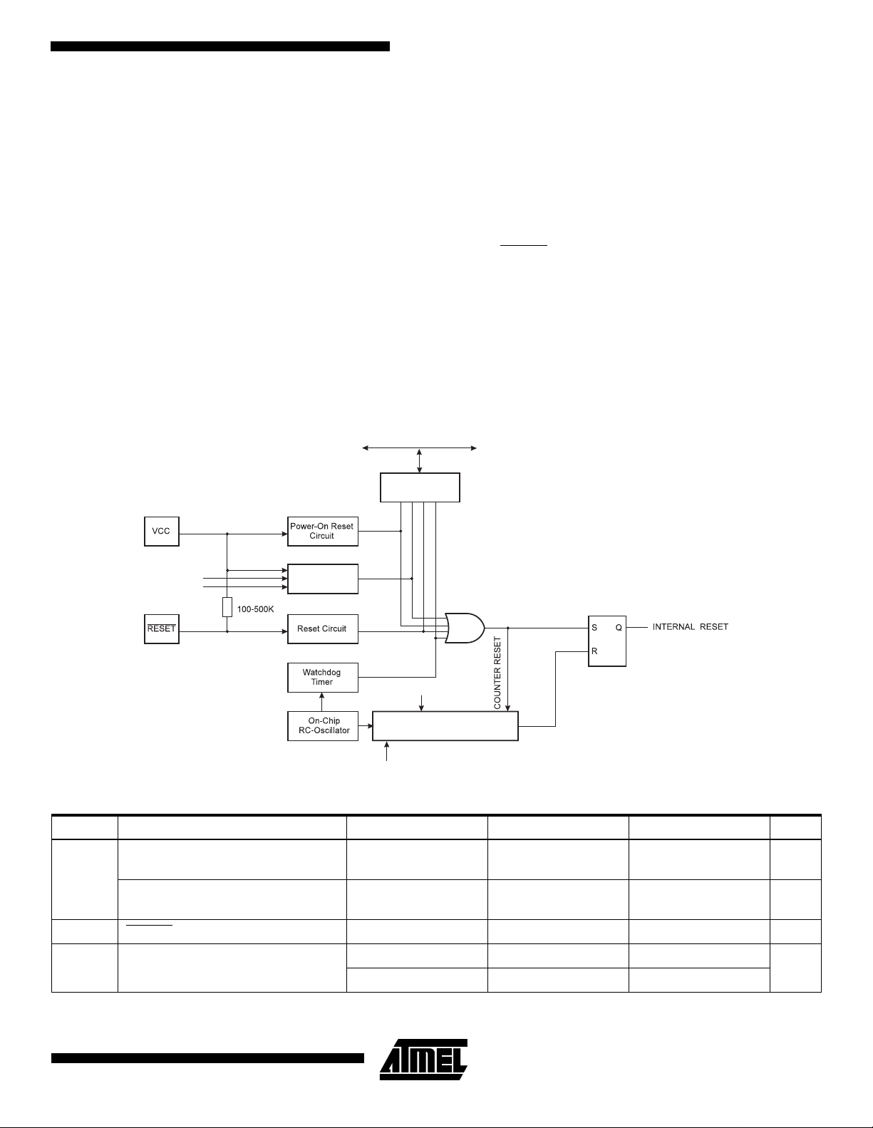
these locations. The circuit diagram in Figure 24 shows the reset logic. Table 4 and Table 5 define the timing and electrical
parameters of the reset circuitry.
Figure 24. Reset Logic
DATA BUS
POT
).
MCU Status
Register (MCUSR)
BORF
PORF
WDRF
EXTRF
BODEN
BODLEVEL
Brown-Out
Reset Circuit
CK
CKSEL[2:0]
Delay Counters
Full
Table 4. Reset Characteristics (VCC = 5.0V)
Symbol Parameter Min Typ Max Units
V
V
V
POT
RST
BOT
Power-On Reset Threshold Voltage,
rising
Power-On Reset Threshold Voltage,
falling
RESET Pin Threshold Voltage 0.6V
2.6 (BODLEVEL = 1) 2.7 (BODLEVEL = 1) 2.8 (BODLEVEL = 1)
Brown-Out Reset Threshold Voltage
3.8 (BODLEVEL = 0) 4.0 (BODLEVEL = 0) 4.2 (BODLEVEL = 0)
1.0 1.4 1.8 V
0.4 0.6 0.8 V
CC
V
V
Note: The Power-On Reset will not work unless the supply voltage has been below Vpot (falling).
19
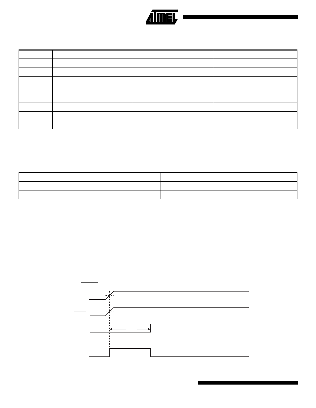
Table 5. Reset Delay Selections
CKSEL [2:0] Star t-Up Time, t
TOUT
at V
= 2.7V Start-Up Time, t
CC
TOUT
at V
= 5.0V Recommended Usage
CC
000 16 ms + 6 CK 4 ms + 6 CK External Clock, slowly rising power
001 6 CK 6 CK External Clock, BOD enabled
(1)
010 256 ms + 16K CK 64 ms + 16K CK Crystal Oscilla tor
011 16 ms + 16K CK 4 ms + 16K CK Crystal Oscillator, fast rising power
100 16K CK 16K CK Crystal Oscillator, BOD enabled
(1)
101 256 ms + 1K CK 64 ms + 1K CK Ceramic Resonator
110 16 ms + 1K CK 4 ms + 1K CK Ceramic Resonator, fast rising power
111 1K CK 1K CK Ceramic Resonator, BOD enabled
(1)
Notes: 1. Or external p ower-on reset.
This table shows the start-up times from reset. From sleep, only the clock counting part of the start-up time is used. The
watchdog oscillator is used for timing the real-time part of the start-up time. The number WDT oscillator cy cles used for
each time-out is shown in Table 6.
Table 6. Number of Watchdog Oscillator Cycles
Time-out Number of cycles
4.0 ms (at V
64 ms (at Vcc=5.0V) 64K
=5.0V) 4K
cc
The frequency of the watchdog oscillator is voltage dependent as shown in the Electrical Characteristics section.
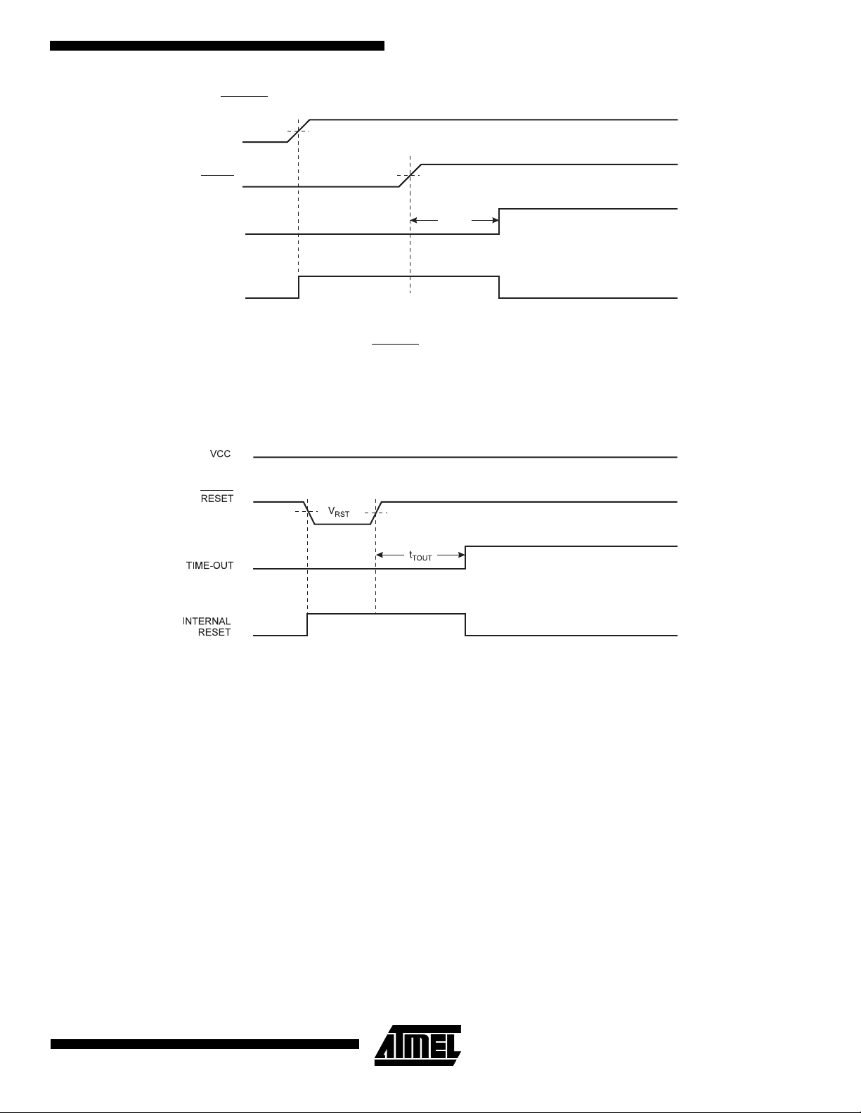
Power-On Reset
A Power-On Reset (POR) pulse is generated by an on-chip detection circuit. The detection l evel is nominal ly 2.2V. The
POR is activated whenever V
is below the detection level. The POR circuit can be used to trigger the start-up reset, as
CC
well as detect a failure in supply voltage.
The Power-On Reset (POR) circuit ensures that the device is reset from power-on. Reaching the power-on reset threshold
voltage invokes a delay cou nter, which determines the delay, for which the device i s kept in RESET after V
rise. The
CC
time-out period of the delay counter is a combination of internal RC oscillator cycles and external oscillator cycles, and it
can be defined by the user through the CKSEL fuses. The eight different selections for the delay period are presented in
Table 5. The RESET signal is activated again, without any delay, when the V
Figure 25. MCU Start-Up, RESET
VCC
RESET
TIME-OUT
INTERNAL
RESET
Tied to VCC.
V
POT
V
RST
t
TOUT
decreases below detection level.
CC
20
AT90S/LS2333 and AT90S/LS4433
AT90S/LS2333 and AT90S/LS4433
Figure 26. MCU Start-Up, RESET
VCC
RESET
TIME-OUT
INTERNAL
RESET
Controlled Externally
V
POT
V
RST
t
TOUT
External Reset
An external reset is generated by a low level on the RESET
pin. Reset pulses longer than 50 ns will generate a reset, even
if the clock is not running. Shorter pulses are not guaranteed to generate a reset.When the applied signal reaches the
Reset Thresh old V oltag e V
on its positive edge, the delay timer starts the MCU after the Time-out period t
RST
TOUT
has
expired.
Figure 27. External Reset During Operation
Brown-Out Detection
AT90S2333/4433 has an on-chip brown-out de tection (BOD ) circui t for monitorin g the V
level during the operati on. Th e
CC
power supply must be decoupl ed with a 47 n F to 100 nF capacitor if th e BOD func tion is used. T he BOD circu it can be
enabled/disabled by the fuse BODEN. W hen BODEN i s enabled (BODEN programmed), and V
below the trigger level, the brown-out reset is immediately activated. When V
increases above the trigger level, the
CC
decreases to a value
CC
brown-out reset is de ac tivate d after a delay. The delay is de fin ed b y the u ser in the sa me way as the delay of PO R s ignal ,
in Table 5. The trigger level for the BOD can be selected by the fuse BODLEVEL to be 2.7V (BODLEVEL unprogrammed),
or 4.0V (BODLEVEL programmed). The trigger level has a hysteresis of 50 mV to ensure spike free brown-out detection.
The BOD circuit will only detect a drop in V
if the voltage stays below the trigger level for longer than 3 µs for trigger level
CC
4.0V, 7 µs for trigger level 2.7V (typical values).
21
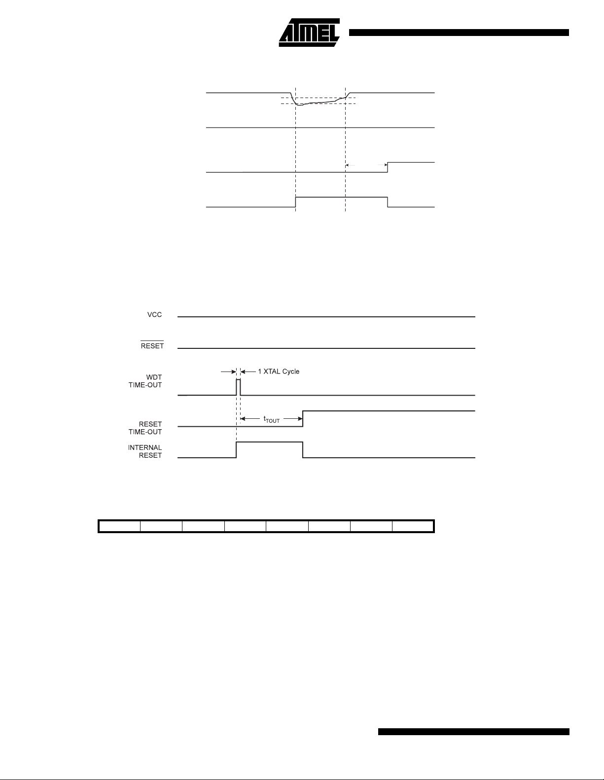
Figure 28. Brown-Out Reset During Operation
VCC
RESET
TIME-OUT
INTERNAL
RESET
V
BOT-
V
t
TOUT
BOT+
Watchdog Reset
When the Watchdo g tim es out, i t will generate a sh ort rese t pulse o f 1 XT AL cyc le durati on. On the falli ng edge of this
pulse, the delay timer starts counting the Time-out period t
. Refer to Page page 36 for details on operation of the
TOUT
Watchdog.
Figure 29. Watchdog Reset During Operation
MCU Status Register - MCUSR
The MCU Status Register provides information on which reset source caused an MCU reset.
Bit 76543210
$34 ($54) - - - - WDRF BORF EXTRF PORF MCUSR
Read/Write R R R R R/W R/W R/W R/W
Initial value 0 0 0 0 See bit description
Bits 7..4 - Res: Reserved Bits
•
These bits are reserved bits in the AT90S2333 and always read as zero.
Bit 3 - WDRF: Watchdog Reset Flag
•
This bit is set if a watchdog reset occurs. The bit is cleared by a power-on reset, or by writing a logic zero to the flag.
Bit 2 - BORF: Brown-Out Reset Flag
•
This bit is set if a brown-out reset occurs. The bit is cleared by a power-on reset, or by writing a logic zero to the flag.
Bit 1 - EXTRF: External Reset Flag
•
This bit is set if an external reset occurs. The bit is cleared by a power-on reset, or by writing a logic zero to the flag.
Bit 0 - PORF: Power-on Reset Flag
•
This bit is set if a power-on reset occurs. The bit is cleared only by writing a logic zero to the flag.
22
AT90S/LS2333 and AT90S/LS4433

AT90S/LS2333 and AT90S/LS4433
To make use of the reset flags to identify a reset condition, the user should read and then clear the MCUSR as early as
possible in the program. If the register is cleared before another reset occurs, the source of the reset can be found by
examining the reset flags.
Interrupt Handling
The AT90S2333/4433 has two 8-bit Interrupt Mask control registers; GIMSK - General Interrupt Mask register and TIMSK Timer/Counter Interrupt Mask register.
When an interrupt occurs, the Global Interrupt Enable I-bit is cleared (zero) and all interrupts are disabled. The user software can set (one) the I-bit to enable nested interrupts. The I-bit is set (one) when a Return from Interrupt instruction - RETI
- is executed.
When the Program Counter is vectored to the actual interrupt vector in order to execute the interrupt handling routine, hard-
ware clears the corresponding flag that generated the interrupt. Some of the interrupt flags can also be cleared by writing a
logic one to the flag bit position(s) to be cleared.
If an interrupt condition occurs when the corresponding interrupt enable bit is cleared (zero), the interrupt flag will be set
and remembered until the interrupt is enabled, or the flag is cleared by software.
If one or more interrupt conditi ons occu r when the global interrupt ena ble bit is clea red (zero), th e correspondi ng interrup t
flag(s) will be set and remembered until the global interrupt enable bit is set (one), and will be executed by order of priority.
Note that external level interrupt does not have a flag, and will only be remembered for as long as the interrupt condition is
active.
Note that the status register is not automatically stored when entering an interrupt routine and restored when returning from
an interrupt routine. This must be handled by software.
General Interrupt Mask Register - GIMSK
Bit 7 6 5 4 3 2 1 0
$3B ($5B) INT1 INT0 - - - - - - GIMSK
Read/Write R/W R/W R R R R R R
Initial value 0 0 0 0 0 0 0 0
•
Bit 7 - INT1: External Interrupt Request 1 Enable
When the INT1 bit is set (one) and the I-bit in the Status Register (SREG) is set (one), the external pin interrupt is enabled.
The Interrupt Sense Control1 bits 1/0 (ISC11 and ISC10) in the MCU general Control Register (MCUCR) defines whet her
the external interrupt is activated on rising or falling edge of the INT1 pin or level sensed. Please note that INTF1 flag is not
set when level sensitive interrupt condition is met. However, INT1 interrupt is generated, provided that INT1 mask bit is set
in GIMSK register. Activity on the pin will cause an i nterrupt request even if INT1 is configured as an output. The corresponding interrupt of External Interrupt Req uest 1 is executed from program mem ory address $002. Se e also “Externa l
Interrupts”.
Bit 6 - INT0: External Interrupt Request 0 Enable
•
When the INT0 bit is set (one) and the I-bit in the Status Register (SREG) is set (one), the external pin interrupt is enabled.
The Interrupt Sense Control0 bits 1/0 (ISC01 and ISC00) in the MCU general Control Register (MCUCR) defines whet her
the external interrupt is activated on rising or falling edge of the INT0 pin or level sensed. Please note that INTF0 flag is not
set when level sensitive interrupt condition is met. However, INT0 interrupt is generated, provided that INT0 mask bit is set
in GIMSK register. Activity on the pin will cause an i nterrupt request even if INT0 is configured as an output. The corresponding interrupt of External Interrupt Req uest 0 is executed from program mem ory address $001. Se e also “Externa l
Interrupts.”
Bits 5..0 - Res: Reserved bits
•
These bits are reserved bits in the AT90S2333/4433 and always read as zero.
23

General Interrupt Flag Register - GIFR
Bit 7 6 5 4 3 2 1 0
$3A ($5A) I NTF1 INTF0 - - - - - - GIFR
Read/Write R/W R/W R R R R R R
Initial value 0 0 0 0 0 0 0 0
•
Bit 7 - INTF1: External Interrupt Flag1
When an event on the INT1 pin triggers an interrupt request, INTF1 becomes set (one). If the I-bit in SREG and the INT1 bit
in GIMSK are set (one), the MCU will jump to the interrupt vector at address $002. The flag is cleared when the interrupt
routine is executed. Alternatively, the flag can be cleared by writing a logical one to it.
Bit 6 - INTF0: External Interrupt Flag0
•
When an event on the INT0 pin triggers an interrupt request, INTF0 becomes set (one). If the I-bit in SREG and the INT0 bit
in GIMSK are set (one), the MCU will jump to the interrupt vector at address $001. The flag is cleared when the interrupt
routine is executed. Alternatively, the flag can be cleared by writing a logical one to it.
Bits 5..0 - Res: Reserved bits
•
These bits are reserved bits in the AT90S2333/4433 and always read as zero.
Timer/Counter Interrupt Mask Register - TIMSK
Bit 7 6 5 4 3 2 1 0
$39 ($59) TOIE1 OCIE1 - - TICIE1 - TOIE0 - TIMSK
Read/Write R/W R/W R R R/W R R/W R
Initial value 0 0 0 0 0 0 0 0
Bit 7 - TOIE1: Timer/Counter1 Overflow Interrupt Enable
•
When the TOIE1 bit is set (one) and the I-bit in the Status Register is set (one), the Timer/Counter1 Overflow interrupt is
enabled. The corresponding interrupt (at vector $005) is executed if an overflow in Timer/Counter1 occurs, i.e., when the
TOV1 bit is set in the Timer/Counter Interrupt Flag Register - TIFR.
Bit 6 - OCIE1: Timer/Counter1 Output Compare Match Interrupt Enable
•
When the OCIE1 bit is set (on e) and the I- bi t in the S tatus Reg ister is set ( one ), th e Tim er/Cou nter 1 Co mpa re Match i nte r-
rupt is enabled. The corresponding interrupt (at vector $004) is executed if a Compare match in Timer/Counter1 occurs,
i.e., when the OCF1 bit is set in the Timer/Counter Interrupt Flag Register - TIFR.
Bit 5, 4 - Res: Reserved Bits
•
These bits are reserved bits in the AT90S2333/4433 and always read as 0.
Bit 3 - TICIE1: Timer/Counter1 Input Capture Interrupt Enable
•
When the TICIE1 bit is set (one) a nd the I-bit in the Statu s Register is set (one), th e Timer/Co unter1 Input Capt ure Event
Interrupt is enabled. The corresponding interrupt (at vector $003) is executed if a capture-triggering event occurs on pin 14,
PB0 (ICP), i.e., when the ICF1 bit is set in the Timer/Counter Interrupt Flag Register - TIFR.
Bit 2 - Res: Reserved Bit
•
This bit is a reserved bit in the AT90S2333/4433 and always reads as 0.
Bit 1 - TOIE0: Timer/Counter0 Overflow Interrupt Enable
•
When the TOIE0 bit is set (one) and the I-bit in the Status Register is set (one), the Timer/Counter0 Overflow interrupt is
enabled. The corresponding interrupt (at vector $006) is executed if an overflow in Timer/Counter0 occurs, i.e., when the
TOV0 bit is set in the Timer/Counter Interrupt Flag Register - TIFR.
Bit 0 - Res: Reserved bit
•
This bit is a reserved bit in the AT90S2333/4433 and always reads as zero.
24
AT90S/LS2333 and AT90S/LS4433

AT90S/LS2333 and AT90S/LS4433
Timer/Counter Interrupt Flag Register - TIFR
Bit 7 6 5 4 3 2 1 0
$38 ($58) TOV1 OCF1 - - ICF1 - TOV0 - TIFR
Read/Write R/W R/W R R R/W R R/W R
Initial value 0 0 0 0 0 0 0 0
•
Bit 7 - TOV1: Timer/Counter1 Overflow Flag
The TOV1 is set (one) when an overflow occu rs i n Tim er /Co unte r1 . TOV1 is c lea red b y h ar dwa re when ex ec uti ng the co rresponding int errupt hand ling vecto r. Alterna tively, TOV 1 is clear ed by writin g a logic one to th e flag. Whe n the I-bit in
SREG, and TOIE1 (T imer/Counter 1 Overflow Inter rupt Enable ), and TOV1 ar e set (one), the Ti mer/Counter 1 Overflow
Interrupt is executed. In PWM mode, this bit is set when Timer/Counter1 advances from $0000.
Bit 6 - OCF1: Output Compare Flag 1
•
The OCF1 bit is set (one) whe n comp ar e ma tch oc c urs b etwe en t he Timer /Co unte r1 an d the dat a i n OCR1 - Out put Com-
pare Registe r 1. OC F1 is cl eared b y har dware when exe cuti ng the c orresp ondi ng inte rrupt hand ling ve ctor. Alter nati vely,
OCF1 is cleared by writing a logic one to the flag. When the I-bit in SREG, and OCIE1 (Timer/Counter1 Compare match
InterruptA Enable), and the OCF1 are set (one), the Timer/Counter1 Compare match Interrupt is executed.
Bit 5, 4 - Res: Reserved Bits
•
These bits are reserved bits in the AT90S2333/4433 and always read as 0.
Bit 3 - ICF1: Input Capture Flag 1
•
The ICF1 bit is set (one) to flag an input capture event, indicating that the Timer/Counter1 value has been transferred to the
input capture register - ICR1. ICF1 is cleared by har dware when executi ng the corresp onding interrupt han dling vector.
Alternatively, ICF1 is cleared by writing a logic one to the flag. When the SREG I-bit, and TICIE1 (Timer/Counter1 Input
Capture Interrupt Enable), and ICF1 are set (one), the Timer/Counter1 Capture Interrupt is executed.
Bit 2 - Res: Reserved Bit
•
This bit is a reserved bit in the AT90S2333/4433 and always reads as 0.
Bit 1 - TOV0: Timer/Counter0 Overflow Flag
•
The bit TOV0 is set (one) when an overflow occurs in Timer/Counter0. TOV0 is cleared by hardware when executing the
corresponding interrupt handling vector. Alternatively, TOV0 is cleared by writing a logic one to the flag. When the SREG Ibit, and TOIE0 (Timer/Counter0 Overflow Interrupt Enable), and TOV0 are set (one), the Timer/Counter0 Overflow interrupt
is executed.
Bit 0 - Res: Reserved bit
•
This bit is a reserved bit in the AT90S2333/4433 and always reads as zero.
External Interrupts
The external interrupts are triggered by the INT1 and INT0 pins. Observe that, if enabled, the interrupts will trigger even if
the INT0/INT1 pins are co nfi gured as ou tputs . Th is fea tur e p rovi de s a way o f ge nerati ng a s oftw ar e i nterr up t. The ex terna l
interrupts c an be t rigg ered by a fal ling or risin g edge or a low leve l. This is set up as i ndica ted in the sp ecifi catio n for th e
MCU Control Register - MCUCR. When the ex ternal int errupt is enabled and is configu red as level trig gered, the interru pt
will trigger as long as the pin is held low.
The external interrupts are set up as described in the specification for the MCU Control Register - MCUCR.
Interrupt Response Time
The interrupt execution res ponse for all the enabl ed AVR interrupts is 4 cloc k cycles minim um. 4 clock cycles after the
interrupt flag h as been set , the pro gram ve ctor addre ss for the actual interru pt handl ing routi ne is exec uted. Du ring this 4
clock cycle period, the Program Counter (2 bytes) is pushed onto the Stack, and the Stack Pointer is decremented by 2.
The vector is normally a relative jump to the interrupt routine, and this jump takes 2 clock cycles. If an interrupt occurs during execution of a multi-cycle instruction, this instruction is completed before the interrupt is served.
A return from an interrupt handling routine (same as for a subroutine call routine) takes 4 clock cycles. During these 4 clock
cycles, the Program Counter (2 bytes) is popped back from the Stack, the Stack Pointer is incremented by 2, and the I flag
in SREG is set . When th e AVR e xits from an inte rrupt, it will alway s return to the mai n program and ex ecute one more
instruction before any pending interrupt is served.
25
MCU Control Register - MCUCR
The MCU Control Register contains control bits for general MCU functions.
Bit 76543210
$35 ($55) - - SE SM ISC11 ISC10 ISC01 ISC00 MCUCR
Read/Write R R R/W R/W R/W R /W R/W R/W
Initial value 0 0 0 0 0 0 0 0
•
Bits 7, 6 - Res: Reserved bit
These bits are reserved bits in the AT90S2333/4433 and always reads as zero.
Bit 5 - SE: Sleep Enable
•
The SE bit must be set (one) to make the MCU enter the sleep mode when the SLEEP instruction is executed. To avoid the
MCU entering the sleep mode unless it is the programmers purpose, it is recommended to set the Sleep Enable SE bit just
before the execution of the SLEEP instruction.
Bits 4 - SM: Sleep Mode
•
This bit selects between the two availabl e sleep modes. Whe n SM is cleared (zer o), Idle Mode is selected as sleep mode.
When SM is set (one), Power Down Mode is selected as Sleep Mode. For details, refer to the paragraph “Sleep Modes”
below.
Bits 3, 2 - ISC11, ISC10: Interrupt Sense Control 1 bit 1 and bit 0
•
The External Interrupt 1 is activated by the external pin INT1 if the SREG I-flag and the corresponding interrupt mask in the
GIMSK is set. The level and edges on the external INT1 pin that activate the interrupt are defined in the following table:
Table 7. Interrupt 1 Sense Control
ISC11 ISC10 Description
0 0 The low level of INT1 generates an interrupt request.
0 1 Any logical change on INT1 generates an interrupt request.
1 0 The falling edge of INT1 generates an interrupt request.
1 1 The rising edge of INT1 generates an interrupt request.
Note: When changing the ISC11/ISC10 bits, INT1 must be disabled by clearing its Interrupt Enable bit in the GIMSK Register. Other-
wise an interrupt can occur when the bits are changed.
The value on the INT1 pin is sampled before detecting edges. If edge or toggle interrupt is selected, pulses that last longer
than one clock period will generate an interru pt. Shorter pulses are not guaranteed to generate an in terrupt. If low leve l
interrupt is selected, the low level must be held until the completion of the currently executing instruction to generate an
interrupt
•
Bits 1, 0 - ISC01, ISC00: Interrupt Sense Control 0 bit 1 and bit 0
The External Interrupt 0 is activated by the external pin INT0 if the SREG I-flag and the corresponding interrupt mask is set.
The level and edges on the external INT0 pin that activate the interrupt are defined in the following table:
Table 8. Interrupt 0 Sense Control
ISC01 ISC00 Description
0 0 The low level of INT0 generates an interrupt request.
0 1 Any logical change on INT0 generates an interrupt request.
1 0 The falling edge of INT0 generates an interrupt request.
1 1 The rising edge of INT0 generates an interrupt request.
Note: When changing the ISC01/ISC00 bits, INT0 must be disabled by clearing its Interrupt Enable bit in the GIMSK Register. Other-
wise an interrupt can occur when the bits are changed.
26
AT90S/LS2333 and AT90S/LS4433

AT90S/LS2333 and AT90S/LS4433
The value on the INT0 pin is sampled before detecting edges. If edge or toggle interrupt is selected, pulses that last longer
than one clock period will generate an interru pt. Shorter pulses are not guaranteed to generate an in terrupt. If low leve l
interrupt is selected, the low level must be held until the completion of the currently executing instruction to generate an
interrupt
Sleep Modes
To enter the sleep modes, the SE bit in MCUCR must be set (one) and a SLEEP instruction must be executed. The SM bit
in the MCUCR register selects which sleep mode (Idle or Power Down) will be activated by the SLEEP instruction. If an
enabled interrupt occur s whi le t he MCU is in a sleep mode, th e MCU a wak es, ex ec utes the int erru pt routine, and resumes
execution from the instruction following SLEEP. On wake-up from Power Down Mode on pin change, the two instructions
following SLEEP are executed before the pin change interrupt routine. The contents of the register file and I/O memory are
unaltered. If a reset occurs during sleep mode, the MCU wakes up and executes from the Reset vector.
Note that if a level triggered interrupt is used for wake-up from power down, the low level must be held for a time longer
than the reset delay time-out period t
Idle Mode
When the SM bit is cleared (zero), the SLEEP instruction forces the MCU into the Idle Mode stopping the CPU but allowing
Timer/Counters, Watchdog and the interrupt system to continue operating. This enables the MCU to wake up from external
triggered interrupts as well as internal ones like Timer Overflow interrupt and watchdog reset. If wake-up from the Analog
Comparator interrupt is not required, the analog comparator can be powered down by setting the ACD-bit in the Analog
Comparator Control and Status register - ACSR. This will reduce power consumption in Idle Mode.
. Otherwise, the device will not wake up.
TOUT
Power Down Mode
When the SM bit is set (one), the SLEEP instruction forces the MCU into the Power Down Mode. In this mode, the external
oscillator is stopped, while the external interrupts and the Watchdog (if enabled) continue operating. Only an external reset,
a watchdog reset (if enabled), an external level interrupt, or a pin change interrupt can wake up the MCU.
Note that if a level triggered or pin change interrupt is used for wake-up from Power Down Mode, the changed level must
be held for a time to wake up the MCU. This makes the MCU less sensitive to noise. The wake-up period is equal to the
clock-counting part of the r eset p er iod ( see Tab le 5 ). The M CU wi ll wake up fr om p owe r-down i f the inp ut h as the re qui red
level for two watchdog osci llator cycles . If the wake up period is shorter than two watchd og oscill ator cycles, the MCU will
wake up if the input has the required level for the duration of the wake-up period. If the wake-up condition disappears
before the wake-up period has expired, the MCU will wake up from power down without executing the corresponding
interrupt.
The period of the watchdog oscillator is 2.7µs (nominal) at 3.0V and 25°C. The frequency of the watchdog oscillator is volt-
age dependent as shown in the Electrical Characteristics section.
When waking up from Powe r Down Mode, ther e is a delay fro m the wake-up conditio n occurs un til the wake-u p becomes
effective. This a llows the clo ck to res tart a nd bec ome stab le aft er ha ving been s topped . The wak e-up pe riod is defi ned by
the same CKSEL fuses that define the reset time-out period.
27
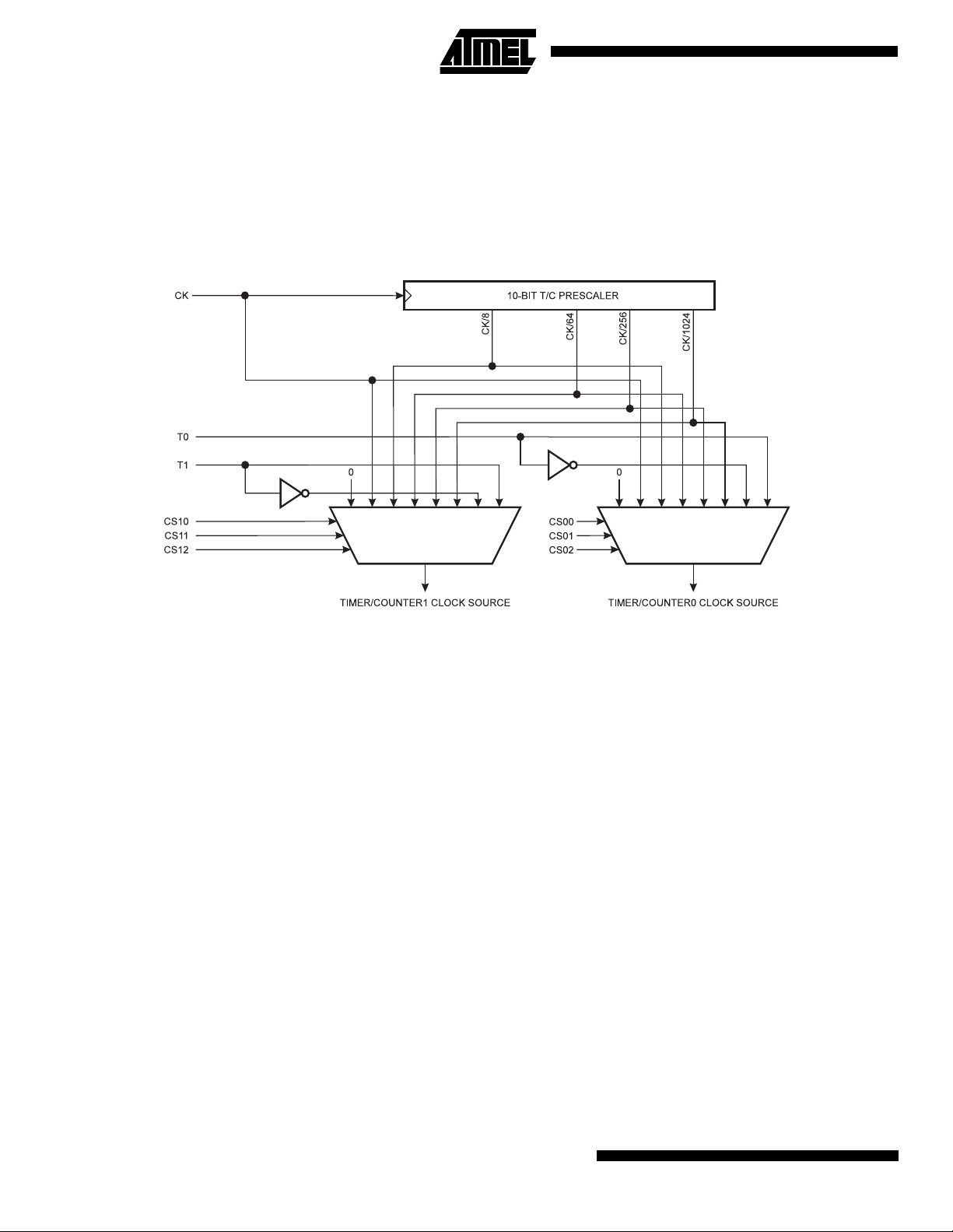
Timer / Counters
The AT90S2333/4433 pr ovid es two general purpose Timer/Cou nter s - one 8- bit T/C and one 16-bit T/C. Timer/ Coun ters 0
and 1 have individual prescaling selection from the same 10-bit prescaling timer. These Timer/Counters can either be used
as a timer with an internal clock timebase or as a counter with an external pin connection which triggers the counting.
Timer/Counter Prescaler
Figure 30. Prescaler for Timer/Counter0 and 1
TCK1
For Timer/Counte rs 0 an d 1, the fou r d iffer ent pres caled sel ection s a re: C K/8, CK /64, CK/2 56 and CK/1 024, whe re CK is
the oscillator clock. For the two Timer/Counters 0 and 1, external source and stop can also be selected as clock sources.
TCK0
8-bit Timer/Counter0
The 8-bit Timer/Counter0 can select cl ock sou rce from CK, presc aled CK , or an exter nal pin. In a dditio n it can b e stoppe d
as described in the specification for the Timer/Counter0 Cont ro l Register - TCCR0. The overflo w status fl ag i s found in the
Timer/Counter Inter rupt Flag Register - TIF R. Contro l signals ar e found in the Timer/Co unter0 Con trol Re gister - TCCR0 .
The interrupt enable/disable settings for Timer/Counter0 are found in the Timer/Counter Interrupt Mask Register - TIMSK.
When Timer/Counter0 is externally clocked, the external signal is synchronized with the oscillator frequency of the CPU. To
assure proper sampling of the external clock, the minimum time between two external clock transitions must be at least one
internal CPU clock period. The external clock signal is sampled on the rising edge of the internal CPU clock.
The 8-bit Timer/Counter0 features both a high resolution and a high accuracy usage with the lower prescaling opportunities. Similarly, t he hig h pr escali ng opp ortuniti es ma ke th e Time r/Coun ter0 us eful fo r lower spe ed fun ctions or e xact tim ing
functions with infrequent actions. Figure 31 shows the block diagram for Timer/Counter0.
28
AT90S/LS2333 and AT90S/LS4433
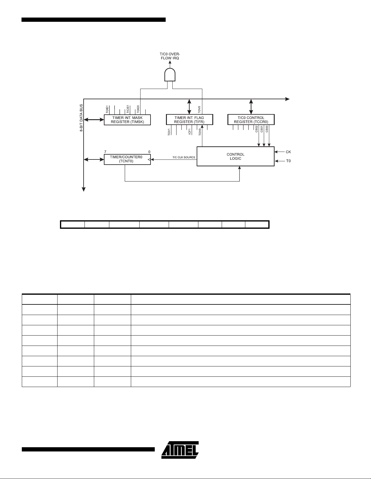
Figure 31. Timer/Counter0 Block Diagram
OCIE1
AT90S/LS2333 and AT90S/LS4433
OCF1
T0
Timer/Counter0 Control Register - TCCR0
Bit 7 6 5 4 3 2 1 0
$33 ($53) - - - - - CS02 CS01 CS00 TCCR0
Read/Write R R R R R R/W R/W R/W
Initial value 0 0 0 0 0 0 0 0
•
Bits 7-3 - Res: Reserved bits
These bits are reserved bits in the AT90S2333/4433 and always read as zero.
Bits 2,1,0 - CS02, CS01, CS00: Clock Select0, bit 2,1 and 0
•
The Clock Select0 bits 2,1, and 0 define the prescaling source of Timer0.
Table 9. Clock 0 Prescale Select
CS02 CS01 CS00 Description
0 0 0 Stop, Timer/Counter0 is stopped.
001CK
0 1 0 CK / 8
011CK / 64
1 0 0 CK / 256
1 0 1 CK / 1024
1 1 0 External Pin T0, falling edge
1 1 1 External Pin T0, rising edge
The Stop condition provides a Timer Enable/Disable function. The prescaled CK modes are scaled direct ly from the CK
oscillator clock. If the external pin modes are used, for Timer/Counter0, transitions on PD4/(T0) will clock the counter even
if the pin is configured as an output. This feature can give the user SW control of the counting.
29
Timer Counter 0 - TCNT0
Bit 76543210
$32 ($52) MSB LSB TCNT0
Read/Write R/W R/W R/W R/W R/W R/W R/W R/W
Initial value 0 0 0 0 0 0 0 0
The Timer/Count er0 is re alized as an up- counter with rea d and wri te acce ss. If the Timer/ Counter 0 is writt en and a clock
source is present, the Timer/Counter0 continues counting in the clock cycle following the write operation.
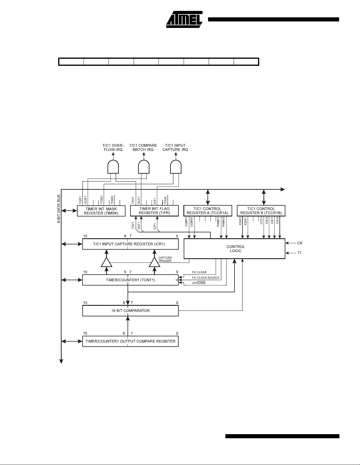
16-bit Timer/Counter1
Figure 32 shows the bl ock diagram for Timer/Counter1.
Figure 32. Timer/Counter1 Block Diagram
T1
The 16-bit Timer/Counter1 can select clock source from CK, prescaled CK, or an external pin. In addition it can be stopped
as described in the specification for the Timer/Counter1 Control Register - TCCR1A. The different status flags (overflow,
compare match and cap ture e vent) and contr ol si gnals ar e found in the Tim er/Co unter Inter rupt Flag R egist er - TIFR. The
interrupt enable/disable settings for Timer/Counter1 are found in the Timer/Counter Interrupt Mask Register - TIMSK.
30
AT90S/LS2333 and AT90S/LS4433
 Loading...