

Page 1

http://www.BDTIC.com/ATMEL
AVR1509: Xplain training - Low Power
Prerequisites
• Required knowledge
Atmel® XMEGA™ Basics training
Atmel XMEGA Clock System
Atmel XMEGA DMAC (Optional, may be needed for understanding task 4)
Atmel XMEGA ADC (Optional, may be needed for understanding task 4)
• Software prerequisites
Atmel AVR
WinAVR/GCC 20100110 or later
• Hardware prerequisites
XPLAIN evaluation board
JTAGICE mkII
• Estimated completion time
2 hours
1 Introduction
Atmel XMEGA provides various sleep modes and software controlled clock gating
in order to tailor power consumption to the application's requirement. Sleep modes
enables the microcontroller to shut down unused modules to save power. When
the device enters sleep mode, program execution is stopped and interrupts or reset
is used to wake the device again. The individual clock to unused peripherals can
be stopped during normal operation or in sleep, enabling a much more fine tuned
power management than sleep modes alone.
®
Studio® 4.18 or later
8-bit
Microcontrollers
Application Note
Refer to application note AVR1010 and XMEGA Datasheet for more in-depth
information.
Rev. 8318A-AVR-06/10
Page 2
2 Introduction to the XMEGA power reduction and sleep system
http://www.BDTIC.com/ATMEL
To reach the lowest possible power figures there are a couple of points to pay
attention to. It is not only the sleep mode that defines the power consumption, but
also the state of the IO pins, number of enabled peripheral modules and so on.
In the following chapters we will look in more detail into the different methods to
reduce power, and try out a few trivial examples.
2.1 General considerations
Regardless of operating mode, two factors especially influence power consumption,
namely CPU and Peripheral clock frequencies and operating voltage.
The power consumption is proportional to operating voltage, and to conserve power
one should consider using as low system voltage as all possible.
Additionally, consumption is also directly proportional to clock frequency, and if sleep
modes are not utilized, the device should be running as low frequency as possible.
2.2 Sleep modes
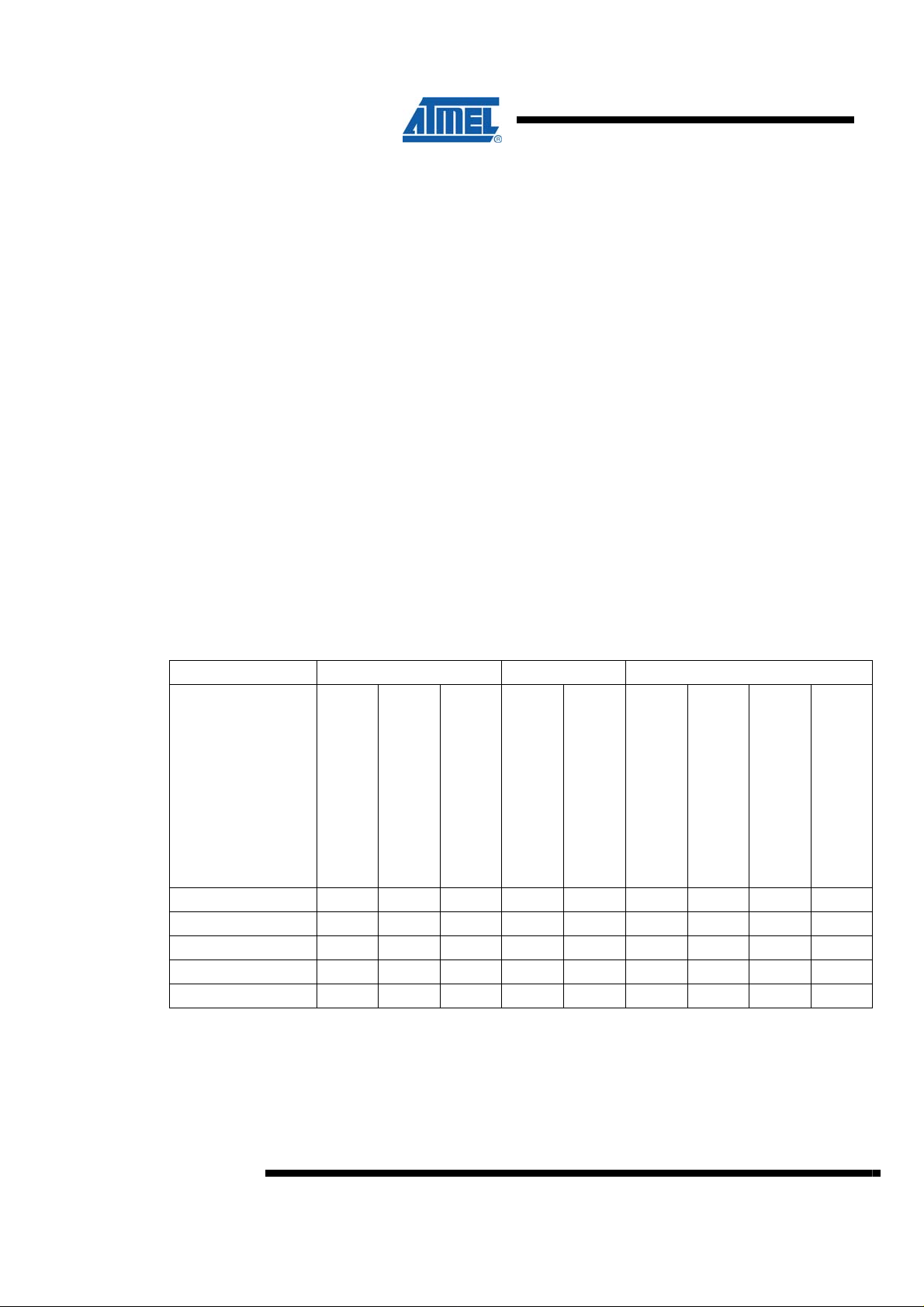
Sleep modes are used to shut down modules and clock domains in the microcontroller in order to tailor power consumption to the applications requirements.
During sleep, various modules are shut down according to which sleep modes are
entered.
2
Active clock domain Oscillators Wake-up sources
Sleep modes
Idle x x x x x x x x
Power-down x x
Power-save x x x x x
Standby x x x
Extended standby x x x x x x
AVR1509
Cpu clock
Peripheral clock
RTC clock
System clock source
RTC clock source
Asynchronous Port Interrupt
TWI Address match interrupts
Real time clock interrupts
All interrupts
Idle Mode
In Idle mode the CPU and Non-Volatile Memory are stopped, (note that any active
programming will be completed) but all peripherals including the Interrupt Controller,
Event System and DMA Controller are kept running. Any interrupt request will wake
the device.
8318A-AVR-06/10
Page 3

Power-down Mode
http://www.BDTIC.com/ATMEL
In Power-down mode all system clock sources, including the Real Time Counter
(RTC) clock source, are stopped. This allows operation of asynchronous modules
only. The only interrupts that can wake up the MCU are the Two Wire Interface
address match interrupts, and asynchronous port interrupts.
Power-save Mode
Power-save mode is identical to Power-down, with one exception: If the RTC is
enabled, it will keep running during sleep and the device can also wake up from either
RTC Overflow or Compare Match interrupt.
Standby Mode
Standby mode is identical to Power-down with the exception that the enabled system
clock sources are kept running, while the CPU, Peripheral and RTC clocks are
stopped. This reduces the wake-up time.
Extended Standby Mode
Extended Standby mode is identical to Power-save mode with the exception that the
enabled system clock sources are kept running while the CPU and Peripheral clocks
are stopped. This reduces the wake-up time.
2.3 Power reduction registers
AVR1509
The Power Reduction (PR) registers provides a method to stop the clock to individual
peripherals. When this is done, the current state of the peripheral is frozen and the
associated I/O registers cannot be read or written. Resources used by the peripheral
will remain occupied; hence the peripheral should in most cases be disabled before
stopping the clock. Enabling the clock to a peripheral again puts the peripheral in the
same state as before it was stopped.
This can be used in Idle mode and Active mode to reduce the overall power
consumption significantly.
In all other sleep modes, the peripheral clock is already stoppe d.
Overview of power reduction registers.
Address Name Bit 7 Bit 6 Bit 5 Bit 4 Bit 3 Bit 2 Bit 1 Bit 0 Page
+0x00 PRGEN - - - AES EBI RTC EVSYS DMA 98
+0x01 PRPA - - - - - DAC ADC AC 99
+0x02 PRPB - - - - - DAC ADC AC 99
+0x03 PRPC - TWI USART1 USART0 SPI HIRES TC1 TC0 99
+0x04 PRPD - TWI USART1 USART0 SPI HIRES TC1 TC0 99
+0x05 PRPE - TWI USART1 USART0 SPI HIRES TC1 TC0 99
+0x06 PRPF - TWI USART1 USART0 SPI HIRES TC1 TC0 99
+0x07 Reserved - - - - - - - -
8318A-AVR-06/10
3
Page 4

2.4 Other power-saving tips
http://www.BDTIC.com/ATMEL
2.4.1 Digital I/O pin
All digital I/O pins are by default floating not to cause any hardware conflicts.
However, because the pins have digital buffers it is important to ensure that the
voltage level on the I/O pins are digitally well defined, as not to cause sporadic
internal switching and leakage. Hence, pull-up should be enabled on all unused pins.
This is mainly observable in sleep modes.
2.4.2 Watchdog Timer
Because the Wat
enabled, contribute to the power consumption in sleep modes.
2.4.3 Brown-Out Detection
c
hdog is basically a timer with a separate clock source it will, if
2.4.4 JTAG interface
2.5 Relevant applications
The purpo
operating at too low voltage.
However, during sleep, the device is “not operating”, or rather, it is not executing
code. For this reason the Atmel XMEGA BOD can be disabled, though enabled
during active mode. The BODACT can also be programmed so the BOD is enabled
automatically in active mode.
The BOD should still be enabled during automatic memory transfers with the DMA
Controller in Idle mode, to avoid data corruption.
The
during operation of the end-product. The JTAG interface is clocked and active during
sleep if enabled.
Note that the JTAG interface can be disabled from software, and still easily be
reprogrammed since the JTAG interface is re-enabled during RESET.
With Atmel XMEGA it is possible to do many common tasks even with the main clock
turned off, in IDLE mode, thanks to the new Event system and DMA controller. By
using the Event system or DMA transfers the firmware will need to wake up the CPU
less frequently.
se of the Brown-Out Detector (BOD) is to ensure that the device is not
JTAG in
terface is used for programming and debugging, but has no function
Power-Save mode is also interesting, as the RTC clock is still powered and can wake
up the CPU on overflow or compare match.
2.6 Measuring current consumption of only XMEGA chip on Xplain
There is a shunt resistor (no. R105), depending on board revision, separating the
XMEGA power-domain from the regulated 3.3 voltage from the USB. To this resistor
there are two test pads connected; IXM+ and IXM-. In this training we will do the
following:
• Solder off the resistor, and solder on a wire to each of the pads.
• Connect the wires through an ampere meter, black lead to wire on IXM-.
4
AVR1509
8318A-AVR-06/10
Page 5

3 Overview
http://www.BDTIC.com/ATMEL
Here is a short overview of the tasks in this training:
Task 1: Introductory sleep-example
This will give a basic understanding of how to select a sleep mode and how it works.
Task 2: Entering and exiting Power-save mode
AVR1509
In this task we will show how to set up the RTC clock source, set up compare
interrupt, set up the sleep register and enter power-save mode.
Task 3: Power Reduction Registers
In this task we will use the Power Reduction Registers to stop the clock going to
peripheral modules and compare with Extended Standby.
Task 4: Idle mode and DMA transfers
In this task we will show you how to set up a simple ADC sampling from the
temperature-resistor on Xplain and set up an automatic memory transfer in idle mode.
We will do the same in Active mode without DMA.
Task 5: TWI Address Match Wakeup
In this task we will wake the Atmel XMEGA from Power-down sleep mode by TWI
address match. To do something useful, we will send button presses.
TIP:
You will have to remove the JTAGICE mkII and sometimes even cycle power to the
Xplain board to observe the expected power consumption levels.
Good luck!
8318A-AVR-06/10
5
Page 6
4 Task 1: Introductory sleep-example
http://www.BDTIC.com/ATMEL
In this task we will demonstrate how to enter a low-power sleep mode and wake up
using asynchronous interrupts.
The goal for this task is that you know how to:
• Select a sleep mode
• Issue sleep-instruction
• Understand wakeup
TASK:
1. Locate the Atmel XMEGA-Lowpower folder, find the Task 1 folder and open the
TrivialSleep.aps project file in AVR Studio
2. Look through the code and ensure you understand how things are set up. Notice
the #define sleep() near the top of the file
3. Build the project; ensure there are no errors. Start the debugging session, singlestep through and look at the Sleep Controller in I/O view
4. When the sleep(); line is executed, nothing happens afterwards. Half the buttons
are set up to generate interrupts. Press one of the buttons on the board and
continue to single step through the code
5. There is an instruction missing at the end of void facilitatePowersaving() to deal
with the potentiometer on the Xplain board. Try to find out what needs to be done
6. Switch between different sleep modes, noting power consumption in the table
below
Active Idle Standby Power-down
7. Compare Idle and Power-down with Electrical Characteristics Section 33.2 of the
A1 datasheet. Remember to add consumption of RC2M to the characteristics for
Ext Clk if applicable. We will find out in task 3
Why don’t the LEDs affect power-consumption as measured going into the XMEGA?
See schematics for Xplain.
why there is a discrepancy
6
AVR1509
8318A-AVR-06/10
Page 7

5 Task 2: Entering and exiting Power-save mode
http://www.BDTIC.com/ATMEL
Atmel XMEGA has many sleep modes. In this task we will show how to set up PowerSave mode and wake up intermittently.
The goal for this task is that you know how to:
• Select a sleep mode
• Enable/disable sleep
• Set up and use RTC-interrupt and understand the program flow
TASK:
1. Locate the XMEGA-Lowpower folder, find the Task 2 folder and open the
Powersave.aps project file in Atmel AVR Studio
2. Look through the code and ensure you understand how things are set up
3. Build the project; ensure there are no errors
AVR1509
4. Add code to select the sleep mode Power Save using the SLEEP_SMODE_t struct
from iox128a1.h located in \WINAVR\avr\include\avr
5. Rebuild and start the debugging session
6. Find out why the LEDs are only blinking when you press and hold down a button.
They should toggle at 2 Hz automatically. Hint: Sleep mode
7. Use the switches to select RTC clock sources, noting power consumption
External on TOSC pins Internal RC Oscillator Internal Ultra Low Power
Why did we need Power-save and not, for example, Power-down or Standby? Which
others would work as well?
8318A-AVR-06/10
7
Page 8
6 Task 3: Power Reduction Registers
http://www.BDTIC.com/ATMEL
Atmel XMEGA features Power Reduction Registers to tailor clock-gating and, by
extension, power-consumption. In this task we will show how to stop the various
peripherals clocks.
The goal for this task is that you know how to:
• Stop clock to undesired peripherals
• Restart clock to peripherals
TASK:
1. Locate the XMEGA-Lowpower folder, find the Task 3 folder and open the
PowerRedReg.aps project file in AVR Studio
2. Look through the code and ensure you understand how things are set up
3. Build the project; ensure there are no errors
4. Start the debugging session
5. Use the switches of selected peripherals. Do you notice any effects? Use button 3
to toggle into Extended Standby and then back into Idle with all peripherals on
again. Note power consumption in the table below
Everything on GEN+TC off COM+ANLG off All off Ext. Standby
What is the difference between sleep modes and shutting off all peripheral clock
gates in active mode?
8
AVR1509
8318A-AVR-06/10
Page 9

7 Task 4: Idle Mode and DMA Transfer
http://www.BDTIC.com/ATMEL
Atmel XMEGA devices include, among other peripherals, a DMA controller which
helps to conserve power and still get the work done. One of these is the DMA
Controller. In this task you will see that even with the main clock turned off, the
microcontroller is able to sample and move data around in memory.
The goal for this task is that you know how to:
• Utilize peripherals even in sleep modes
TASK:
1. Locate the XMEGA-Lowpower folder, find the Task 4 folder and open the
IdleDMA.aps project file in AVR Studio
2. Look through the code and ensure you understand how things are set up
AVR1509
3. Build the project; ensure there are no errors
4. Start the debugging session
5. Use the switches to switch between Active and Idle mode. Note power
consumption in the table below and compare with electrical characteristics and
previous measurements
Active Idle
6. Touch the temperature sensor (right by the potentiometer) or blow on it to heat it
up. Check that you get corresponding result on the LEDs
Does the sampling and copying continue when in Idle mode? How?
Why is an interrupt needed to enter Active mode from Idle?
8318A-AVR-06/10
9
Page 10

8 Task 5: TWI Address Match Wakeup
http://www.BDTIC.com/ATMEL
One of the advantages of TWI is that it is asynchronous and clocked externally. The
Atmel XMEGA takes advantage of this, and provides a wakeup interrupt on address
match, even in the lowest power Power-Down mode.
The goal for this task is that you know how to:
• Set up TWI and address match interrupt using the driver from the application note
TASK:
1. Locate the XMEGA-Lowpower folder, find the Task 5 folder and open the
TwiWake.aps project file in Atmel AVR Studio
2. Look through the code and ensure you understand how things are set up
3. Build the project; ensure there are no errors
9 Summary
4. Connect the pins on the header marked XMEGA PORT D to another Xplain board
on the same pins. Either using a 10-pin cable or using single jumper cables,
connect PD0 to PD0, PD1 to PD1 and GND to GND. If desirable, one Xplain can
work without USB power, but be powered by connecting V3P3 to V3P3 on the
XMEGA PORT D header
5. Start the debugging session. Make yourself comfortable with the program flow.
Note that we can’t sleep again until the TWI transaction is finished
6. Disconnect the JTAGICE mkII and cycle power to the Xplain. Now you should see
a power consumption of approximately 0.1 µA when not pressing any buttons
Why do we have to manage the sleep enable bit manually for slave transactions?
In this training we have looked at some of the ways we can conserve power on the
XMEGA, including sleep modes, stopping the clock to peripherals and disabling
various other modules when not needed. We have also seen that many tasks can
easily be accomplished even when utilizing low-power sleep modes.
10
AVR1509
8318A-AVR-06/10
Page 11

10 Resources
http://www.BDTIC.com/ATMEL
• Atmel XMEGA Manual and Datasheets
o http://www.atmel.com/xmega
• Atmel AVR Studio with help files
o http://www.atmel.com/products/AVR/
• WINAVR GCC compiler
o http://winavr.sourceforge.net/
• Atmel IAR Embedded Workbench
o http://www.iar.com/
11 Atmel Technical Support Center
Atmel has several support channels available:
®
compiler
AVR1509
• Web portal: http://support.atmel.no/
• Email: avr@atmel.com
• Email: avr32@atmel.com
Please register on the web portal to gain access to the following services:
• Access to a rich FAQ database
• Easy submission of technical support requests
• History of all your past support requests
• Register to receive Atmel microcontrollers’ newsletters
• Get information about available trainings and training material
All Atmel AVR products
All Atmel microcontrollers
All 32-bit AVR products
8318A-AVR-06/10
11
Page 12

http://www.BDTIC.com/ATMEL
Disclaimer
Headquarters International
Atmel Corporation
2325 Orchard Parkway
San Jose, CA 95131
USA
Tel: 1(408) 441-0311
Fax: 1(408) 487-2600
Atmel Asia
Unit 1-5 & 16, 19/F
BEA Tower, Millennium City 5
418 Kwun Tong Road
Kwun Tong, Kowloon
Hong Kong
Tel: (852) 2245-6100
Fax: (852) 2722-1369
Atmel Europe
Le Krebs
8, Rue Jean-Pierre Timbaud
BP 309
78054 Saint-Quentin-enYvelines Cedex
France
Tel: (33) 1-30-60-70-00
Fax: (33) 1-30-60-71-11
Atmel Japan
9F, Tonetsu Shinkawa Bldg.
1-24-8 Shinkawa
Chuo-ku, Tokyo 104-0033
Japan
Tel: (81) 3-3523-3551
Fax: (81) 3-3523-7581
Product Contact
Web Site
www.atmel.com
Disclaimer: The information in this document is provided in connection with Atmel products. No license, express or implied, by estoppel or otherwise, to any
intellectual property right is granted by this document or in connection with the sale of Atmel products. EXCEPT AS SET FORTH IN ATMEL’S TERMS AND
CONDITIONS OF SALE LOCATED ON ATMEL’S WEB SITE, ATMEL ASSUMES NO LIABILITY WHATSOEVER AND DISCLAIMS ANY EXPRESS, IMPLIED
OR STATUTORY WARRANTY RELATING TO ITS PRODUCTS INCLUDING, BUT NOT LIMITED TO, THE IMPLIED WARRANTY OF MERCHANTABILITY,
FITNESS FOR A PARTICULAR PURPOSE, OR NON-INFRINGEMENT. IN NO EVENT SHALL ATMEL BE LIABLE FOR ANY DIRECT, INDIRECT,
CONSEQUENTIAL, PUNITIVE, SPECIAL OR INCIDENTAL DAMAGES (INCLUDING, WITHOUT LIMITATION, DAMAGES FOR LOSS OF PROFITS,
BUSINESS INTERRUPTION, OR LOSS OF INFORMATION) ARISING OUT OF THE USE OR INABILITY TO USE THIS DOCUMENT, EVEN IF ATMEL HAS
BEEN ADVISED OF THE POSSIBILITY OF SUCH DAMAGES. Atmel makes no representations or warranties with respect to the accuracy or completeness of the
contents of this document and reserves the right to make changes to specifications and product descriptions at any time without notice. Atmel does not make any
commitment to update the information contained herein. Unless specifically provided otherwise, Atmel products are not suitable for, and shall not be used in,
automotive applications. Atmel’s products are not intended, authorized, or warranted for use as components in applications intended to support or sustain life.
© 2010 Atmel Corporation. All rights reserved. Atmel®, Atmel logo and combinations thereof, AVR®, AVR® logo, AVR Studio® and others, are
the registered trademarks, XMEGA™ and others are trademarks of Atmel Corporation or its subsidiaries. Other terms and product names may
be trademarks of others.
Literature Request
www.atmel.com/literature
Technical Support
avr@atmel.com
Sales Contact
www.atmel.com/contacts
8318A-AVR-06/10
 Loading...