

Page 1

Introduction
This document contains the latest information about the AVR data book and the AVR
data sheets.
®
All references to the data book refers to the August 1999 version of the “AVR
MICROCONTROLLER DATA BOOK”.
All references to the A VR data she ets refer to the latest version of the AVR d ata
sheets on Atmel’s web page www.atmel.com
.
RISC
The data she ets on Atmel’s w eb pa ge are updated more frequen tly than the p rinted
data book. All known errors in each data sheet are corrected wh en a new v ersion is
released.
This document contains known errors that have not been corrected yet. All designers
using AVR microcontrollers should use this document together with the data sheets. It
is updated frequently, and should contain a complete list of all known documentation
errors at any given time.
Please note that this document only covers errors in the AVR documentation. For
errors in the AVR microcontrollers, see the errata sheet for each device.
If you find errors in the documentation that are not listed in this document, please
send an email to the AVR support line avr@atmel.com
.
Overview of data sheets
Part Number Data Sheet Revision
in the August 1999
AVR Data Book
AT90S1200 0838E-04/99 0838E-04/99
AT90S2313 0839E-04/99 0839E-04/99
AT90S/LS2323 and AT90S/LS2343 1004B-04/99 1004B-04/99
AT90S/LS2333 and AT90S/LS4443 1042D-04/99 1042D-04/99
AT90S4414/8515 0841E-04/99 0841E-04/99
AT90S/LS4434 and AT90S/LS8535 1041E-04/99 1041E-04/99
AT90C8534 1229A-04/99 1229A-04/99
ATtiny10/11/12 1006A-04/99 1006B-10/99
ATtiny15 1187A-06/99 1187B-11/99
ATtiny22/22L 1273A-04/99 1273A-04/99
ATmega161/161L 1228A-05/99 1228A-08/99
ATmega603/603L and ATmega103/103L 0945D-06/99 0945E-12/99
AVR Instruction Set 0856B-06/99 0856B-06/99
ATtiny28 N/A 1062B-10/99
Data Sheet Revision
on Atmel’s web site
www.atmel.com
8-Bit
Microcontroller
Data
Book Updates
and Changes
Rev. 12/99A
1
Page 2

AT90S1200
The latest data sheet on the web is rev. 0838E-04/99.
The data sheet in the printed data book is rev. 0838E-04/99.
Changes in the AT90S1200 Data Sheet:
Page: Change or Add:
2-3 In feature list under
I/O and packages,
replace “20-pin PDIP and SOIC” by “20-pin PDIP, SOIC and SSOP”.
2-20 Table 4: remove this note: “Not e: When ch anging the ISC01/ ISC00 bit s, INT0 must be disabl ed by cl earing its Int er-
rupt Enable bit in the GIMSK registe r. Otherwise an interrupt can occur when the bits are changed. ”
2-25 In the note for Table 6, add “To avoid unintenti onal MCU resets, the Watchdog Timer should be disabled or reset
before changing the Watchdog Timer Prescale Select.”
In the
EEPROM Read/Write Access
description,
change
“When the EEPROM is read or written, the CPU is
halted for two clock cycles before the next instruction is executed.” to “When the EEPROM is written, the CPU is
halted for two clock cycles before the next instruction is executed. When the EEPROM is read, the CPU is halted
for four clock cycles before the next instruction is executed.”
2-26 In the
Bit 0 - EERE: EEPROM Read Enable
description,
change
“When EERE has been set, the CPU i s halt ed f or
two clock cycles before the next instruction is executed.” to “When EERE has been set, the CPU is halted for four
clock cycles before the next instruction is executed.”
2-27 In the
Analog Comparator Control and Status Register
description, change the initial value of ACO from “0” to
“N/A”.
2-29 in the
2-33 in the
Port B Input Pins Address - PINB
Port D Input Pins Address - PIND
description, change the Initial Values from “Hi-Z” to “N/A”.
description, change the Initial Values of bits 0 to 6 from “Hi-Z” to “N/A”.
2-44 Replace figure 34 by the one below:
Figure
34 Serial Programming and Verify
VCC
PB7
PB6
PB5
2.7 - 6.0
SCK
MISO
MOSI
AT90S1200
GND
CLOCK INPUT
2
Data Book Updates and Changes
RESET
XTAL1
GND
Page 3

Data Book Updates and Changes
2-49: Replace the row bel ow in
V
ACIO
Analog Comparator
Input Offset Voltage
by:
V
ACIO
2-50 In first l ine of
Analog Comparator
Input Offset Voltage
Typical Characteristics
are not tested during manufacturing.”.
2-62 In
Register Summary
, replace “2-2-xx” by “2-xx”.
DC characteristics
VCC = 5V 40 mV
VCC = 5V
Vin = VCC /2
:
40 mV
, change “These data are characterized, but not tested.” to “These figures
3
Page 4

AT90S2313
The latest data sheet on the web is rev. 0839E-04/99.
The data sheet in the printed data book is rev. 0839E-04/99.
Changes in the AT90S2313 Data Sheet:
Page: Change or Add:
3-28 Table 5: remove this note: “Note: W hen changing th e ISC11/ISC10 bits, INT1 must be disable d by clea ring it s Inter -
rupt Enable bit in the GIMSK registe r. Otherwise an interrupt can occur when the bits are changed. ”
3-29 Table 6: remove this note: “Not e: When ch anging the ISC01/ ISC00 bit s, INT0 must be disabl ed by cl earing its Int er-
rupt Enable bit in the GIMSK registe r. Otherwise an interrupt can occur when the bits are changed. ”
3-38 On the top of the page, add paragraph “Note: If the compare register contains the TOP value and the prescaler is
not in use (CS12..CS10 = 001), the PWM output will not produce any pulse at all, because the up-counting and
down-counting values are reached simultaneously. When the prescaler is in use (CS12..CS10 ≠ 001 or 000), the
PWM output goes active when the counter reaches the TOP value, but the down-counting compare match is not
interpreted to be reached before the next time the counter reaches the TOP-value, making a one period PWM
pulse.”
3-39 In the note for Table 14, add “To avoid unintentional MCU resets, the Watchdog Timer should be disabled or reset
before changing the Watchdog Timer Prescale Select.”
In the
halted for two clock cycles before the next instruction is executed.” to “When the EEPROM is written, the CPU is
halted for two clock cycles before the next instruction is executed. When the EEPROM is read, the CPU is halted
for four clock cycles before the next instruction is executed.”
3-40 In the
EECR” to “4. Write a lo gical on e to the EEMWE bit in EECR (to be a ble to wr ite a l ogical one to the EEMWE bit, t he
EEWE bit must be written to zero in the same cycle).”
3-41 In the
two clock cycles before the next instruction is executed.” to “When EERE has been set, the CPU is halted for four
clock cycles before the next instruction is executed.”
3-47 In the
“N/A”.
3-49 in the
3-54 in the
3-67 Replace figure 34 by the one below:
EEPROM Read/Write Access
Bit1 - EEWE: EEPROM Write Enable
Bit 0 - EERE: EEPROM Read Enable
Analog Comparator Control and Status Register
Port B Input Pins Address - PINB
Port D Input Pins Address - PIND
description,
description,
description, change the Initial Values from “Hi-Z” to “N/A”.
description, change the Initial Values of bits 0 to 6 from “Hi-Z” to “N/A”.
change
description,
“When the EEPROM is read or written, the CPU is
change
change
description, change the initial value of ACO from “0” to
“4. Write a logical one to the EEMWE bit in
“When EERE has been set, the CPU i s halt ed f or
4
Data Book Updates and Changes
Page 5

Data Book Updates and Changes
Figure
53 Serial Programming and Verify
3-72: Replace the row bel ow in
V
ACIO
Analog Comparator
Input Offset Voltage
by:
V
ACIO
Analog Comparator
Input Offset Voltage
GND
CLOCK INPUT
DC characteristics
AT90S2313
RESET
XTAL1
GND
:
VCC
PB7
PB6
PB5
2.7 - 6.0
SCK
MISO
MOSI
VCC = 5V 40 mV
VCC = 5V
Vin = VCC /2
40 mV
3-73 In first l ine of
are not tested during manufacturing.”.
3-84 In
Register Summary
Typical Characteristics
, replace “3-3-xx” and “3-3-3-xx” by “3-xx”.
, change “These data are characterized, but not tested.” to “These figures
5
Page 6

AT90S/LS2323 and AT90S/LS2343
The latest data sheet on the web is rev. 1004B-04/99.
The data sheet in the printed data book is rev. 1004B-04/99.
Changes in the AT90S/LS2323 and AT90S/LS2343 Data Sheet:
Page: Change or Add:
4-6 In the
4-7 In the
4-19 In Figure 20, add a box containin g “+1” as a n input to the summation operator.
4-25 In the first paragraph of
4-29 Table 9: remove this note: “Not e: When ch anging the ISC01/ ISC00 bit s, INT0 must be disabl ed by cl earing its Int er-
Pin Descriptions AT90S/LS2323
“Port B is a 3-bit bi-directional I/O port with internal pull-up resistors. The Port B output buffers can sink 20 mA. As
inputs, Port B pins that are externally pulled low, will source current if the pull -up resistors are activated.
Port B also serves the functions of various special features.
Port pins can provide internal pull-up resistors (selected for each bit). The port B pins are tri-stated when a reset
condition becomes acti ve.”
Pin Descriptions AT90S/LS2343
“Port B is a 5-bit bi-directional I/O port with internal pull-up resistors. The Port B output buffers can sink 20 mA. As
inputs, Port B pins that are externally pulled low, will source current if the pull -up resistors are activated.
Port B also serves the functions of various special features.
Port pins can provide internal pull-up resistors (selected for each bit). The port B pins are tri-stated when a reset
condition becomes acti ve.”
Watchdog Reset
pulse of 1 XTAL cycle duration.” by “When the Watchdog times out, it will generate a short reset pulse of 1 CPU
clock cycle duration.”
rupt Enable bit in the GIMSK registe r. Otherwise an interrupt can occur when the bits are changed. ”
replace the description for
replace the description for
, replace “When the Watchdog times out, it will generate a short reset
Port B (PB2..PB0)
Port B (PB4..PB0)
by
by
4-34 In the note for Table 11, add “To avoid unintenti onal MCU resets, the Watchdog Timer should be disabled or reset
before changing the Watchdog Timer Prescale Select.”
In
EEPROM Read/Write Access
two clock cycles before the next instruction is executed.” by “When the EEPROM is written, the CPU is halted for
two clock cycles before t he ne xt instruction is executed. When it is read, the CPU is halted for 4 clock cycles.”.
4-35 In the
EECR” to “4. Write a logica l one to the EEMWE bit i n EECR (to be able to wri te a logical one to the EEMWE bit, the
EEWE bit must be written to zero in the same cycle).”
In the
two clock cycles before the next instruction is executed.” to “When EERE has been set, the CPU is halted for four
clock cycles before the next instruction is executed.”
4-37 in the
6
Bit1 - EEWE: EEPROM Write Enable
Bit 0 - EERE: EEPROM Read Enable
Port B Input Pins Address - PINB
Data Book Updates and Changes
, replace the 6th line “When the EEPROM is read or written, the CPU is halted for
description, change “4. Write a logical one to the EEMWE bit in
description,
description, change the Initial Values of bits 0-4 from “Hi-Z” to “N/A”.
change
“When EERE has been set, the CPU i s halt ed f or
Page 7

Data Book Updates and Changes
4-38 Replace the secti on name “MISO - Port B, Bit 1” by “MISO/INT0 - Port B, Bit 1”
4-40 In
High-Voltage Serial Programming
“Power-up sequence: Apply 4.5 - 5.5V betwee n V
Then, if the RCEN Fuse is not programmed; Toggle XTAL1/PB3 at least 4 times with minimum 100ns pulse-width.
Set PB3 to “0”. Wait at least 100ns.
or if the RCEN Fuse is programmed; Set PB3 to “0”. Wait at least 4µs.
In both cases; Then apply 12V to RESET
any instructions.”
4-40 In
High-Voltage Serial Programming
4-42 In table 16, replace the entries
Read Fuse and
Lock bits
(AT90S/
LS2323)
Read Fuse and
Lock bits
(AT90S/
LS2343)
PB0
PB1
PB2
PB0
PB1
PB2
0_0000_0100_00
0_0100_1100_00
x_xxxx_xxxx_xx
0_0000_0100_00
0_0100_1100_00
x_xxxx_xxxx_xx
by the entries (Note: Bit 7 in the 4’th and 5’th column for PB1 has been inverted compared to the origi nal data
book)
, replace item 1. by
and wait at least 100 ns before changing PB0. Wait 8 µs before giving
, replace in item 5 “Set PB5 to “1”.” by “Set RESET
0_0000_0000_00
0_0110_1000_00
x_xxxx_xxxx_xx
0_0000_0000_00
0_0110_1000_00
x_xxxx_xxxx_xx
and GND. Set RESET and PB0 to “0” and wait at least 100 ns.
CC
to “0”.”
0_0000_0000_00
0_0110_1100_00
S
xx_xxFx_xx
1_2
0_0000_0000_00
0_0110_1100_00
S
xx_xxRx_xx
1_2
Reading
Fuse/Lock bit is programmed.
Reading
Fuse/Lock bit is programmed.
, S, F =’ 0’ means the
1, 2
, S, R =’ 0’ means the
1, 2
Read Fuse and
Lock bits
(AT90S/
LS2323)
Read Fuse and
Lock bits
(AT90S/
LS2343)
PB0
PB1
PB2
PB0
PB1
PB2
0_0000_0100_00
0_0100_1100_00
x_xxxx_xxxx_xx
0_0000_0100_00
0_0100_1100_00
x_xxxx_xxxx_xx
0_0000_0000_00
0_0111_1000_00
x_xxxx_xxxx_xx
0_0000_0000_00
0_0111_1000_00
x_xxxx_xxxx_xx
0_0000_0000_00
0_0111_1100_00
S
xx_xxFx_xx
1_2
0_0000_0000_00
0_0111_1100_00
S
xx_xxRx_xx
1_2
Reading
Fuse/Lock bit is programmed.
Reading
Fuse/Lock bit is programmed.
, S, F =’ 0’ means the
1, 2
, S, R =’ 0’ means the
1, 2
4-43 In figure 35, remove “CLOCK INPUT”, “XTAL1/PB3” and the arrow connecting them.
4-49 In first l ine of
Typical Characteristics
, change “These data are characterized, but not tested.” to “These figures
are not tested during manufacturing.”.
4-59 In Register Summary, replace all “4-page” by “page”. In addition, for TIMSK; replace ”page 4 -15” by “page 4-28”,
for TIFR; replace “page 4-16” by “page 4-28”, for MCUCR; replace “page 4-16” by “page 4-29”, for MCUSR;
replace “page 4-14” by “page 4-26”.
4-60 In Instruction Set Summary under BRANCH INSTRUCTIONS, replace
CPSE Rd,Rr Compare, Skip if Equal if (Rd = Rr) PC
SBRC Rr, b Skip if Bit in Register Cleared if (Rr(b)=0) PC
SBRS Rr, b Skip if Bit in Register is Set if (Rr(b)=1) PC
SBIC P, b Skip if Bit in I/O Register Cleared if (P(b)=0) PC
SBIS P, b Skip if Bit in I/O Register is Set if (R(b)=1) PC
PC + 2 or 3 None 1 / 2
←
PC + 2 or 3 None 1 / 2
←
PC + 2 or 3 None 1 / 2
←
PC + 2 or 3 None 1 / 2
←
PC + 2 or 3 None 1 / 2
←
by
CPSE Rd,Rr Compare, Skip if Equal if (Rd = Rr) PC
SBRC Rr, b Skip if Bit in Register Cleared if (Rr(b)=0) PC
PC + 2 or 3 None 1 / 2 / 3
←
PC + 2 or 3 None 1 / 2 / 3
←
7
Page 8

SBRS Rr, b Skip if Bit in Register is Set if (Rr(b)=1) PC ← PC + 2 or 3 None 1 / 2 / 3
SBIC P, b Skip if Bit in I/O Register Cleared if (P(b)=0) PC
SBIS P, b Skip if Bit in I/O Register is Set if (R(b)=1) PC
PC + 2 or 3 None 1 / 2 / 3
←
PC + 2 or 3 None 1 / 2 / 3
←
8
Data Book Updates and Changes
Page 9

Data Book Updates and Changes
AT90S/LS2333 and AT90S/LS4433
The latest data sheet on the web is rev. 1042D-04/99.
The data sheet in the printed dat a b ook is rev. 1042D-04/99.
Changes in the AT90S/LS2333 and AT90S/LS4433 Data Sheet:
Page: Change or Add:
5-6 In “
5-15 In
5-28 Table 7: remove this note: “Note: When changing the ISC11/ISC10 bi ts, INT1 must be disabled by clearing its Inter-
5-34 In “
5-37 Before
5-39 In the note for Table 16, add “To avoid unintentional MCU resets, the Watchdog Timer should be disabled or reset
5-41 In the
Pin Descriptions
nected to Vcc via a low-pass filter.” to “This is the supply voltage for Port A and the A/D Convert er. If the ADC is not
used, this pin must be connected to Vcc. If the ADC is used, this pin should be connected to Vcc via a low-pass filter.”
Figure 20
rupt Enable bit in the GIMSK register. Otherwise an interrupt can occur when the bits are changed. ”
Table 8: remove this note: “Note: W hen changi ng the I SC01/ISC00 bi ts, I NT0 must be dis abled by cl ear ing it s Inter -
rupt Enable bit in the GIMSK register. Otherwise an interrupt can occur when the bits are changed. ”
Timer/Counter Control Register 1B - TCCR1B
set to divide by 8 from “...C-1 | C, 0, 0, 0, 0, 0, 0, 0, 0 | ...” to “...C-1 | C, 0, 0, 0, 0, 0, 0, 0 | ...”
use (CS12..CS10 = 001), the PWM output will not produce any pulse at all, because the up-counting and downcounting values are reached simultaneously. When the prescaler is in use (CS12..CS10 ≠ 001 or 000), the PWM
output goes active when the counter reaches the TOP value, but the down-counting compare match is not i nterpreted to be reached before the next time the counter reaches the TOP-value, making a one- period PWM pulse.”
before changing the Watchdog Timer Prescale Select.”
EECR” to “4. Write a logical one to the EEMWE bit i n EECR (to be able to writ e a logical one to the EEMWE bit , the
EEWE bit must be written to zero in the same cycle).”
, add a box containing “+1” as an input to the summation operator.
table 14
Bit1 - EEWE: EEPROM Write Enable
”,
, add paragraph “Note: If the compare register contains the TOP value and the prescaler is not in
, change “This is the supply vo ltage f or the A/D Conver ter. It should be externally con -
AVCC
”, bit3 -
description, change “4. Write a logical one to the EEMWE bit in
, change the count sequence when prescaler is
CTC1
5-47..50 In the
5-50 In last line, replace “UBRRH” by “UBRRHI”.
5-52 In “
5-59 In “
5-60 In
5-61 In the
5-66 In the
5-68 In the
5-80 In “
Analog Comparator Control and Status Register - ACSR
ADC Noise Canceling Techniques
Figure 49
Port B Input Pins Address - PINB
Port C Input Pins Address - PINC
Values “Q” to “0” (zero).
Port D Input Pins Address - PIND
Serial Downloading
description, replace “USR” by “UCSRA” and “UCR” by “UCSRB” everywhere.
UART
” item 3, replace “Figure 47” by “Fi gure 49”.
, replace the resistor by a 10 µH inductor. Change capacitor value from 10 nF to 100 nF.
description, change the Ini tial Values from “Hi-Z” to “N/A”.
description, change the Initial Values from “Hi-Z” to “N/A”. Change Initial
description, change the Ini tial Values from “Hi-Z” to “N/A”.
”, replace Figure 66 by the figu re below.
”, the initia l va l ue o f
ACO
is “N/A”.
9
Page 10
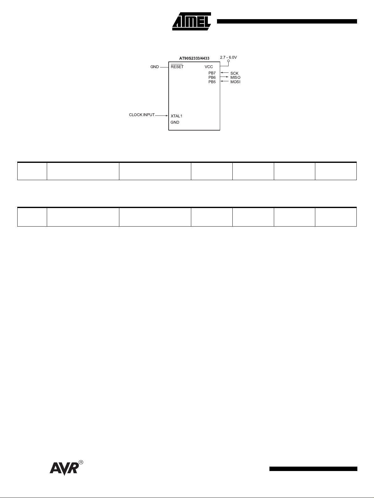
Figure 66. Serial Progr amming and Verify
GND
AT90S2333/4433
RESET
VCC
PB7
PB6
PB5
2.7 - 6.0V
SCK
MISO
MOSI
5-86 Replace the row below in
V
ACIO
Analog Comparator
Input Offset Voltage
by:
V
ACIO
5-86 In “
5-88 In first line of
Analog Comparator
Input Offset Voltage
DC Characteristics
Typical Characteristics
”, footnote 4, r eplace “IOL” by “IOH” everywhere.
are not tested during manufacturing.”.
CLOCK INPUT
DC characteristics
XTAL1
GND
:
VCC = 5V 40 mV
VCC = 5V
Vin = VCC /2
40 mV
, change “These data are characterized, but not tested.” to “These figures
10
Data Book Updates and Changes
Page 11

AT90S4414/8515
The latest data sheet on the web is rev. 0841E-04/99.
The data sheet in the printed dat a b ook is rev. 0841E-04/99.
Changes in the AT90S4414/8515 Data Sheet:
Page: Change or Add:
Data Book Updates and Changes
6-17 In
6-29 Table 6: remove this note: “Note: When changing the ISC11/ISC10 bi ts, INT1 must be disabled by clearing its Inter-
6-30 Table 7: remove this note: “Note: W hen changi ng the I SC01/ISC00 bi t s, INT0 must be dis able d by clear ing it s Inter -
6-39 Before
6-41 In the note for Table 15, add “To avoid unintentional MCU resets, the Watchdog Timer should be disabled or reset
6-42 In the
6-43 In the
Figure 19
rupt Enable bit in the GIMSK register. Otherwise an interrupt can occur when the bits are changed. ”
rupt Enable bit in the GIMSK register. Otherwise an interrupt can occur when the bits are changed. ”
use (CS12..CS10 = 001), the PWM output will not produce any pulse at all, because the up-counting and downcounting values are reached simultaneously. When the prescaler is in use (CS12..CS10 ≠ 001 or 000), the PWM
output goes active when the counter reaches the TOP value, but the down-counting compare match is not i nterpreted to be reached before the next time the counter reaches the TOP-value, making a one- period PWM pulse.”
before changing the Watchdog Timer Prescale Select.”
In the
halted for two clock cycles before the next instruction is executed.” to “When the EEPROM is written, the CPU is
halted for two clock cycles bef ore the next instruction is executed. When the EEPROM is read, the CPU is halted
for four clock cycles before the next instruction is executed.”
EECR” to “4. Write a log ica l one to t he EEMWE bit in EECR (t o be able t o writ e a logic al one to t he EEMWE bit , the
EEWE bit must be written to zero in the same cycle).”
two clock cycles before the next instruction is executed.” to “When EERE has been set, the CPU is halted for four
clock cycles before the next instructi on is executed.”
, add a box containing “+1” as an input to the summation operator.
table 14
EEPROM Read/Write Access
Bit1 - EEWE: EEPROM Write Enable description, change
Bit 0 - EERE: EEPROM Read Enable
, add paragraph “Note: If the compare register contains the TOP value and the prescaler is not in
description,
description,
change
“When the EEPROM is read or written, the CPU is
change
“When EERE has been set, the CPU i s halt ed fo r
“4. Write a logical one to the EEMWE bit in
6-54 In the
6-57 in the
6-59 in the
6-64 in the
6-66 in the
6-79 Replace
Analog Comparator Control and Status Register
“N/A”.
Port A Input Pins Address - PINA
Port B Input Pins Address - PINB
Port C Input Pins Address - PINC
Port D Input Pins Address - PIND
figure 64
description, change the ini tial value of ACO from “0” to
description, change the Initial Values from “Hi-Z” to “N/A”.
description, change the Initial Values from “Hi-Z” to “N/A”.
description, change the Initial Values from “Hi-Z” to “N/A”.
description, change the Initial Values from “Hi-Z” to “N/A”.
by the one below:
11
Page 12

Figure
64 Serial Programming and Verify
6-84: Replace the row below in
V
ACIO
Analog Comparator
Input Offset Voltage
by:
V
ACIO
6-88 In first line of
Analog Comparator
Input Offset Voltage
Typical Characteristics
are not tested during manufacturing.”.
GND
CLOCK INPUT
DC characteristics
AT90S4414/8515
RESET
XTAL1
GND
:
VCC
PB7
PB6
PB5
2.7 - 6.0
SCK
MISO
MOSI
VCC = 5V 40 mV
VCC = 5V
Vin = VCC /2
40 mV
, change “These data are characterized, but not tested.” to “These figures
6-98 In
Register Summary
, replace all “6-6-xx” by “6-xx”.
12
Data Book Updates and Changes
Page 13

Data Book Updates and Changes
AT90S/LS4434 and AT90S/LS8535
The latest data sheet on the web is rev. 1041E-04/99.
The data sheet in the printed dat a b ook is rev. 1041E-04/99.
Changes in the AT90S/LS4434 and AT90S/LS8535 Data Sheet:
Page: Change or Add:
7-6 In “
7-15 In
7-27 In “
7-29 Table 9: remove this note: “Note: When changing the ISC11/ISC10 bi ts, INT1 must be disabled by clearing its Inter-
7-30 In the
7-30 At the end of the
7-36 In “
Pin Descriptions
nected to Vcc via a low-pass filter.” to “This is the supply voltage for Port A and the A/D Convert er. If the ADC is not
used, this pin must be connected to Vcc. If the ADC is used, this pin should be connected to Vcc via a low-pass filter.”
Figure 19
Timer/Counter Inter rupt Flag Regi ster - TIFR
to “Bit 6 - TOV2: T imer /Counter2 Overflow Flag”.
rupt Enable bit in the GIMSK register. Otherwise an interrupt can occur when the bits are changed. ”
Table 10: remove this note: “Note: When changing the ISC01/ISC00 bits, INT0 must be disabled by clearing its
Interrupt Enable bit in the GIMSK register. Otherwise an interrupt can occur when the bits are changed.”
to “Note th at when a level triggered interrupt is use d for wake-up from power down, the low level must be held for a
time longer than the reset delay time- out period t
chronously, Power Down Mode is recom mended instead of Power Save Mode because the contents of the registers in the asynchronous timer should be considered undefined after wake up in Power Save Mode, even if AS2 is
0.”
Timer/Counter Control Register 1B - TCCR1B
set to divide by 8 from “...C-1 | C, 0, 0, 0, 0, 0, 0, 0, 0 | ...” to “...C-1 | C, 0, 0, 0, 0, 0, 0, 0 | ...”
, add a box containing “+1” as an input to the summation operator.
Power Down Mode
”,
Power Save Mode
, change “This is the supply vo ltage f or the A/D Conver ter. It should be externally con -
AVCC
section, replace paragraph 2 (“Note that if a level triggered interrupt... ...on page 7-98.”)
”, change heading “Bit 6 - T OV2: Timer/Counter0 Overflow Flag”
.”
TOUT
section, add the paragraph “If the asynchronous timer is NOT clocked asyn-
”, bit3 -
, change the count sequence when prescaler is
CTC1
7-39 Before
use (CS12..CS10 = 001), the PWM output will not produce any pulse at all, because the up-counting and downcounting values are reached simultaneously. When the prescaler is in use (CS12..CS10 ≠ 001 or 000), the PWM
output goes active when the counter reaches the TOP value, but the down-counting compare match is not i nterpreted to be reached before the next time the counter reaches the TOP-value, making a one- period PWM pulse.”
7-45 Replace last paragraph on page:
“When asynchronous operation is selected, the 32 kHz oscillator for Timer/Counter2 is always running, except in
power down mode. After a power up reset or wake-up from power down, the user should be aware of the fact that
this oscillator might take as long as one second to stabilize. Therefore, the content of all Timer/Counter2 regist ers
must be considered lost after a wake-up from power down, due to the unstable clock signal. The user is advised to
wait for at least one second before usi ng Timer/Counter2 after power-up or wake-up from power down.”
by
“When the asynchronous operation is selected, the 32kHZ oscillator for Timer/Counter2 is always running, except
in power down mode. After a power up reset or wake-up from power down, the user should be aware of the fact
that this osci llator might take as long as one second to stabilize. The user is advised to wait for at least one second
before using Timer/Counter2 after power-up or wake-up from power down. The contents of all Timer /Counter2 reg-
table 16
, add paragraph “Note: If the compare register contains the TOP value and the prescaler is not in
13
Page 14

isters must be co nsidered los t after a wake-up fr om power do wn due to un stab le c lock si gnal upon st art-u p, r egar dless of whether the oscillator is in use or a clock signal is applied to the TOSC pin.”
7-47 In the note for Table 22, add “To avoid unintentional MCU resets, the Watchdog Timer should be disabled or reset
before changing the Watchdog Timer Prescale Select.”
7-49 In the
EECR” to “4. Write a logica l one to the EEMWE bit i n EECR (to be able to wri te a logical one to the EEMWE bit, the
EEWE bit must be written to zero in the same cycle).”
In the
Bit 0 - EERE: EEPROM Read Enable
two clock cycles before the next instruction is executed.” to “When EERE has been set, the CPU is halted for four
clock cycles before the next instruction is executed.”
7-52 Change
Figure 40. SPI Transfer Format with CPHA = 1 and DORD = 0
7-60 In “
Analog Comparator Control and Status Register - ACSR
Bit1 - EEWE: EEPROM Write Enable description
Figure 40
description,
to the figure below.
change
, change “4. Write a logical one to the EEMWE bit in
“When EERE has been set, the CPU i s halt ed f or
”, the initial value of
ACO
is “N/A”.
7-67 In
Figure 50
7-69 In the
7-71 In the
7-76 In the
7-79 In the
7-91 In “
Serial Downloading
Figure 71. Serial Progr amming and Verify
, replace the resistor by a 10 µH inductor. Change capacitor value from 10 nF to 100 nF.
Port A Input Pins Address - PINA
Port B Input Pins Address - PINB
Port C Input Pins Address - PINC
Port D Input Pins Address - PIND
description, change the Initial Values from “Hi-Z” to “N/A” .
description, change the Initial Values from “Hi-Z” to “N/A” .
description, change the Initial Values from “Hi-Z” to “N/A” .
description, change the Initial Values from “Hi-Z” to “N/A” .
”, replace Figure 71 by the fig ure below.
VCC
PB7
PB6
PB5
2.7 - 6.0V
SCK
MISO
MOSI
CLOCK INPUT
GND
AT90S4434/8535
RESET
XTAL1
GND
14
Data Book Updates and Changes
Page 15

Data Book Updates and Changes
7-96 Replace the row bel ow in
V
ACIO
Analog Comparator
Input Offset Voltage
DC characteristics
VCC = 5V 40 mV
:
by:
V
ACIO
Analog Comparator
Input Offset Voltage
7-98 In first l ine of
Typical Characteristics
VCC = 5V
Vin = VCC /2
40 mV
, change “These data are characterized, but not tested.” to “These figures
are not tested during manufacturing.”.
7-109 In Register Summary, replace all “7-page” by “page”. In addition, replace “page 7-337-” by “page 7-33”, “page 7-
377-” by “page 7-37”, “page 7-387-” by “page 7-38”, “page 7-467-” by “page 7-46”, “page 7-487-” by “page 7-48”.
15
Page 16

AT90C8534
The latest data sheet on the web is rev. 1229A-04/99.
The data sheet in the printed data book is rev. 1229A-04/99.
Changes in the AT90C8534 Data Sheet:
Page: Change or Add:
8-5 In “
8-16 In Figure 19, add a box containin g “+1” as a n input to the summation operator.
8-26 At the end of the
8-31 In the
8-32 In the
Pin Descriptions
connected to Vcc via a low-pass filter.” to “This is the supply voltage for the A/D Converter. If the ADC is not used,
this pin must be connected to Vcc. If the ADC is used, this pin should be connect ed to Vcc via a low-pass filter.”
can occur. Therefore, it is recommended to first disable INT1 by clearing its Interrupt Enable bit in the GIMSK register. Then, the ISC1 bit can be changed. Finally, the INT1 interrupt flag should be cleared by writing a logical one
to its Interrupt Flag bi t in the GIFR register before the interrupt is re-enabled.”
At the end of the
can occur. Therefore, it is recommended to first disable INT0 by clearing its Interrupt Enable bit in the GIMSK register. Then, the ISC0 bit can be changed. Finally, the INT0 interrupt flag should be cleared by writing a logical one
to its Interrupt Flag bi t in the GIFR register before the interrupt is re-enabled.”
EEPROM Read/Write Access
halted for two clock cycles before the next instruction is executed.” to “When the EEPROM is written, the CPU is
halted for two clock cycles before the next instruction is executed. When the EEPROM is read, the CPU is halted
for four clock cycles before the next instruction is executed.”
Bit1 - EEWE: EEPROM Write Enable description
EECR” to “4. Write a logica l one to the EEMWE bit i n EECR (to be able to wri te a logical one to the EEMWE bit, the
EEWE bit must be written to zero in the same cycle).”
In the
Bit 0 - EERE: EEPROM Read Enable
two clock cycles before the next instruction is executed.” to “When EERE has been set, the CPU is halted for four
clock cycles before the next instruction is executed.”
”,
AV CC, change
Interrupt Sense Control 1
Interrupt Sense Control 0
“This is the supply voltage for the A/D Converter. It should be externally
description,
description,
description add this text: “When changing the ISC1 bit, an interrupt
description add this text: “When changing the ISC0 bit, an interrupt
change
“When the EEPROM is read or written, the CPU is
, change “4. Write a logical one to the EEMWE bit in
change
“When EERE has been set, the CPU i s halt ed f or
16
Data Book Updates and Changes
Page 17

Data Book Updates and Changes
ATtiny10/11/12
The latest data sheet on the web is rev. 1006B-10/99.
The data sheet in the printed dat a b ook is rev. 1006A-04/99.
Changes in the ATtiny10/11/12 Data Sheet on the web:
Page: Change or Add:
27 Table 13: remove this note: “Note: When changing the ISC01/ISC00 bits, INT0 must be disabled by clearing its
Interrupt Enable bit in the GIMSK register. Otherwise an interrupt can occur when the bits are changed.”
In the first paragraph of
“On wake-up from Power Down Mode on pin change, the two instructions following SLEEP are executed before
the pin change interrupt routine.
by
“On wake-up from Power Down Mode on pi n change, 2 i nstruc ti on cycle s are ex ecuted bef ore the pi n chang e inter -
rupt flag is updated. During these cycles, the processor executes instructions, but the interrupt condition is not
readable, and the interrupt routine has not started yet.
32 In the note for Table 16, add “To avoid unintentional MCU resets, the Watchdog Timer should be disabled or reset
33 In the last sentence of the first paragra ph, chan ge “When the EEPROM is read or writt en, the CPU is halted for two
clock cycles before the next instruction is executed.” to “When the EEPROM is written, the CPU is halted for two
clock cycles before the next instruction is executed. When the EEPROM is read, the CPU i s halted for four clock
cycles before the next instruction is executed.”
In the
EEPROM Control Register
34 In the
Bit 0 - EERE: EEPROM Read Enable
two clock cycles before the next instruction is executed.” to “When EERE has been set, the CPU is halted for four
clock cycles before the next instructi on is executed.”
Sleep modes for the ATtiny10/11
description, change the in itial value of EEWE from “0” to “X”.
description,
section, replace the sent ence
change
“When EERE has been set, the CPU i s halt ed fo r
Changes in the ATtiny10/11/12 section in the data book
Page: Change or Add:
9-3 In both
9-14 In Figure 12, add a box containing “+1” a s an input to the summation operator.
9-24 In the first line of the
In Figure 22, change “1 XTAL Cycle” to “1 CK Cycle”.
9-29 Table 13: remove this note: “Note: When changing the ISC01/ISC00 bits, INT0 must be disabled by clearing its
Interrupt Enable bit in the GIMSK register. Otherwise an interrupt can occur when the bits are changed.”
In the first paragraph of
Pin Configuration
figures, replace RESET with RESET
Watchdog Reset
Sleep modes for the ATtiny10/11
section, change “1 XTAL cycle” to “1 CK cycle”.
.
section, replace the sent ence
17
Page 18

“On wake-up from Power Down Mode on pin change, the two instructions following SLEEP are executed before
the pin change interrupt routine.
by
“On wake-up from Power Down Mode on pin chan ge, 2 i nstruc tion cy cle s are execut ed before the pi n change int er-
rupt flag is updated. During these cycles, the processor executes instructions, but the interrupt condition is not
readable, and the interrupt routine has not started yet.
9-34 In the note for Table 15, add “To avoid unintentional MCU resets, the Watchdog Timer should be disabled or reset
before changing the Watchdog Timer Prescale Select.”
In the first paragraph of
ATtiny12 Calibrated Internal RC Oscillator
section, add “For details on how to use the
pre-programmed calibration value, see the section ‘Calibrati on Byte in ATtiny12’ on page 9-42.
In the second paragraph, add “The calibrated oscillator is used to time EEPROM access. If EEPROM is written, do
not calibrate to m ore than 10% above the nominal frequency. Otherwise, the EEPROM write may fail. Table 1
shows the range for OSCCAL. Note that the Oscillator is intended for calibration to 1.0MHz, thus tuning to other
values is not guaranteed.
Table 1.
Internal RC Oscillator Frequency Range.
OSCCAL value Min. Frequency Max Frequency
$00 0.5MHz 1.0MHz
$7F 0.7MHz 1.5MHz
$FF 1.0MHz 2.0MHz
9-35 In the second line, change “The write access time is in the range of 2.5 - 4ms, depending on the V
time is in the range of 1.9 - 3.4ms, depending on the frequency of the calibrated RC oscillator.”
In the last sentence of the first paragra ph, chan ge “When the EEPROM is read or writt en, the CPU is halted for two
clock cycles before the next instruction is executed.” to “When the EEPROM is written, the CPU is halted for two
clock cycles before the next instruction is executed. When the EEPROM is read, the CPU is halted for four clock
cycles before the next instruction is executed.”
In the
EEPROM Control Register
9-36 In the 14th line, remove “(typically 2.5ms at V
description, change the initial value of EEWE from “0” to “X”.
= 5V or 4 ms at V
CC
= 2.7V)”
CC
.” to “The write access
CC
In the
Bit1 - EEWE: EEPROM Write Enable description
EECR” to “4. Write a logica l one to the EEMWE bit i n EECR (to be able to wri te a logical one to the EEMWE bit, the
EEWE bit must be written to zero in the same cycle).”
In the
Bit 0 - EERE: EEPROM Read Enable
two clock cycles before the next instruction is executed.” to “When EERE has been set, the CPU is halted for four
clock cycles before the next instruction is executed.”
9-37 In the
Analog Comparator Control and Status Register
“N/A”.
9-39 In the
Port B Input Pins Address - PINB
9-40 In the first li ne of section
Port B pins are connected to a p in ch ange detect or t hat can t rigger the pin ch ange i nterr upt. See ‘ Pin Change Int er rupt’ on page 9-28 for detai ls. In addition, Port B has the following alternate functi ons:”.
18
Data Book Updates and Changes
description,
description, change the Initial Value of bits 0-5 from “Hi-Z” to “N/A”.
Alternate Functions of Port B
, change “4. Write a logical one to the EEMWE bit in
change
“When EERE has been set, the CPU i s halt ed f or
description, change the initial value of ACO from “0” to
, change “The alternate pin functions of Port B are:” to “All
Page 19

Data Book Updates and Changes
9-42 In the section
Calibration Byte in ATtiny12
, add “At start-up, the user software must read this flash location and
write the value to the OSCCAL register.”
In the section
ATtiny10/11
, change “The +12V is used for programming enable only, and no current of significance is
drawn by this pin.” to “Only minor currents (<1mA) are drawn from the +12V pin during programming.”.
9-44 In Table 21, remove the entire first row. In the first cell of the second row, remove “(ATtiny12)”.
9-45 In the note on the bottom of the page, change “9, 6 = RSTISBL Fuse” to “9, 6 = RSTDISBL Fuse”.
9-46 In Table 22, remove the “t
WLWH_CE
“row.
In Figure 30, remove “CLOCK INPUT”, “PB3 (XTAL1)” and the arrow connecting them.
9-47 In the sixth line, change “Either an external clock is supplied at pin XTAL1 or a crystal needs to be connected
across pins XTAL1 and XTAL2” to “The device can be clocked by any clock option during Low-Voltage Serial Programming.”.
In the two last lines of the fir st paragraph, change “2 XTAL clock cycles” to “2 CK clock cycles” .
In the first entr y of the
Low-Voltage Serial Programming Algorithm
, change “If a crystal is not connected across
pins XTAL1 and XTAL2, apply a clock signal to the XTAL1 pin.” to “I n accordance with the setting of CKSEL fuses,
apply a crystal/resonator, external clock or RC network, or let the device run on the internal RC oscillator.”.
In the fifth entry, change the fir st “t
and t
WD_EEPROM
”.
WD_PROG
” to “t
WD_FLASH
or t
WD_EEPROM
”. Change the second “t
WD_PROG
” to “t
WD_FLASH
9-48 In the
“t
WD_PROG
Data Polling
” to “t
section, change the first “t
WD_EEPROM
”.
WD_PRO G
9-50 Replace Table 25 and Table 26 with these tables:
Symbol Minimum Wait Delay
t
WD_ERASE
Symbol Minimum Wait Delay
t
WD_FLASH
t
WD_EEPROM
9-52 In the
Symbol Parameter Condit ion Min Typ Max Units
I
CC
DC Characteristics
Power Supply Current
table, replace
Active 4MHz, V
Idle 4MHz, V
Power Down
3V, WDT enabled
Power Down
3V. WDT disabled
CC
(5)
(5)
” to “t
WD_FLA SH
or t
WD_EEPROM
”. Change the second and third
3.4 ms
1.7 ms
3.4 ms
= 3V 3.0 mA
CC
= 3V 1.0 1.2 mA
, V
=
, V
CC
CC
=
9.0 15
<1 2
µ
A
µ
A
19
Page 20

Symbol Parameter Condition Min Typ Max Units
Vacio
Iaclk
Tacpd
Analog Comp
Input Offset V
Analog Comp
Input leakage A
Analog Comp
Propagation Del.
VCC = 5V 40 mV
VCC = 5V
VIN = VCC/2
VCC = 2.7V
VCC = 4.0V
-50 50 nA
750
500
with
Symbol Parameter Condition Min Typ Max Units
Active 1MHz, V
(A Ttiny1 2V)
Active 2MHz, V
(ATtiny10/11L)
Active 4MHz, V
(ATtiny12L)
Active 6MHz, V
(A Ttiny1 0/11)
Active 8MHz, V
(ATtiny12)
Idle 1MHz, V
(AT tiny12V)
I
CC
Power Supply Current
Idle 2MHz, V
(ATtiny10/11L)
Idle 4MHz, V
(ATtiny12L)
CC
CC
CC
= 3V
CC
= 3V
CC
= 3V
CC
= 5V
CC
= 5V
CC
= 3V
= 3V
= 3V
TBD mA
TBD mA
3.0 mA
TBD mA
TBD mA
TBD mA
TBD mA
1.0 1.2 mA
ns
V
ACIO
I
ACLK
T
ACPD
Analog Comparator
Input Offset Voltage
Analog Comparator
Input Leakage Current
Analog Comparator
Propagation Delay
Idle 6MHz, V
CC
= 5V
(AT tiny10/11)
Idle 8MHz, V
CC
= 5V
(ATtiny12)
Power Down
(5)
, V
3V, WDT enabled
Power Down
(5)
, V
3V. WDT disabled
VCC = 5V
VIN = VCC/2
VCC = 5V
VIN = VCC/2
VCC = 2.7V
VCC = 4.0V
CC
CC
TBD mA
TBD mA
=
=
9.0 15
<1 2
µ
A
µ
A
40 mV
-50 50 nA
750
500
ns
20
Data Book Updates and Changes
Page 21

Data Book Updates and Changes
9-53 In the first table, change the title from “External Clock Drive” to “External Clock Dri ve ATtiny12” and add this table:
External Clock Drive ATtiny10/11
VCC = 2.7V to 4.0V VCC = 4.0V to 5.5V
Symbol Parameter
1/t
CLCL
t
CLCL
t
CHCX
t
CLCX
t
CLCH
t
CHCL
Oscillator Frequency 0206MHz
Clock Period 500 167 ns
High Time 200 67 ns
Low Time 200 67 ns
Rise Time 1.6 0.5
Fall Time 1.6 0.5
UnitsMin Max Min Max
s
µ
s
µ
9-54 In the first l ine, change “These data are characterized, but not tested.” to “These figures are not tested during manufactur-
ing.”.
9-72 In row 12 (MCUSR) of the table, change “WDTR” to “WDRF” and “BODR” to “BORF”.
21
Page 22

ATtiny15L
The latest data sheet on the web is rev. 1187B-11/99.
The data sheet in the printed data book is rev. 1187A-06/99.
Changes in the ATtiny15L Data Sheet on the web:
None.
Changes in the ATtiny15L section in the data book:
The data sheet for ATtiny15 has gone through serious imp rovements and corrections since the printi ng of the “AVR
RISC MICROCONTROLLER DATA BOOK AUGUST 1999”. The user is advised to download the complete new
ATtiny15 data sheet from the Web, since correcti ng the present data book would not give a user friendly result.
22
Data Book Updates and Changes
Page 23

Data Book Updates and Changes
ATtiny22/22L
The latest data sheet on the web is rev. 1273A-04/99.
The data sheet in the printed dat a b ook is rev. 1273A-04/99.
Changes in the ATtiny22/22L Data Sheet:
Generally: The external clock option does not exist in ATtiny22/L. Therefore, all references to the RCEN fuse and external
clock are wrong, and the part comes as ATtiny22L only, not ATtiny22.
Page: Change or Add:
All For all “ATtiny22/L” read “ATtiny22L”.
11-3 In the feature list, replace the following lines
•
Special Microcontroller Features
–...
– Selectable On-chip RC Oscillator
•
Power Consumption at 4 MHz, 3V, 25°C
– Active: 2.4 mA
– Idle Mode: 0.5 mA
– Power Down Mode: <1 µA
•
Operating Voltages
– 2.7 - 6.0V (ATtiny22L )
– 4.0 - 6.0V (ATtiny22)
•
Speed Grades
– 0 - 4 MHz (ATtiny22L)
– 0 - 8 MHz (ATtiny22)
by the following description;
•
Special Microcontroller Features
–...
– On-chip RC Oscillator
•
Power Consumption at 3V, 25°C
– Active: 1.5 mA
– Idle Mode: 100µA
– Power Down Mode: <1 µA
•
Operating Voltages
– 2.7 - 6.0V
•
Speed Grade
– Internal Oscillator ~1MHz@5.0V
11-3 Replace
Pin Configuration
by the figure shown below.
RESET
PB3
PB4
GND
1
2
3
4
8
7
6
5
VCC
PB2 (SCK/T0)
PB1 (MISO/INT0)
PB0 (MOSI)
23
Page 24

11-5 In the
“Port B is a 5-bit bi-directional I/O port with internal pull-up resistors. The Port B output buffers can sink 20 mA. As
inputs, Port B pins that are externally pulled low, will source current if the pull -up resistors are activated.
Port B also serves the functions of various special features.
Port pins can provide internal pull-up resistors (selected for each bit). The port B pins are tri-stated when a reset
condition becomes acti ve.”
Pin Descriptions ATtiny22/L
replace the descript ion for
Port B (PB4..PB0)
by
11-5 Remove the description “CLOCK” under
11-5 The whole section “
“
Clock Source
Clock options
Pin Descriptions ATtiny22/L.
“ including Figure 2 should be replaced by
The ATtiny22L is clocked by an on-chip RC oscillator. This RC oscillator runs at a nominal frequency
of 1 MHz (VCC = 5V).“
11-16 In Figur e 18, add a box containing “+1” as an input to the summation operator.
11-16 Replace second paragraph under
Memory Access and Instruction Execution Timing
, “The AV R C P U is drive n
by the System Clock Ø, directly generated from the external clock signal applied to the CLOCK pin.” by “The AVR
CPU is driven by the System Clock Ø, directly gener ated from the internal RC oscilla tor . “
11-21 In Power-On Reset, replace the first paragraph; ”The ATtiny22/L is designed for use in systems where it can oper-
ate from the internal RC oscillator or in applications where a clock signal is provided by an external clock source.
After V
by an external clock source, the clock must not be applied until V
has reached V
CC
, the device will start after the time t
POT
(see Figure 23). If the clock signal is provided
TOUT
has reached the minimum voltage defined for
CC
the applied frequency. “ by “The ATtiny22L is desig ned f or use in sys tems where i t can o perat e from th e inte rnal RC
oscillator. After V
has reached V
CC
, the device will start after the time t
POT
(see Figure 23).”
TOUT
11-23 In the first paragraph of Watchdog Reset, replace “When the Watchdog times out, it will generate a short reset
pulse of 1 CPU cycle duration.” by “When the Watchdog times out, it will generate a short reset pulse of 1 clock
cycle duration.”
11-27 Table 7: remove thi s no te: “Not e: When ch angi ng the ISC01/ISC00 bi ts, I NT0 must be disabl ed by cl earing its Int er -
rupt Enable bit in the GIMSK registe r. Otherwise an interrupt can occur when the bits are changed. ”
11-31 In the note for Table 9, add “To avoid unintentional MCU resets, the Watchdog Timer should be disabled or reset
before changing the Watchdog Timer Prescale Select.”
11-32 In line num ber 6, replace “When the EEPROM is read or written, the CPU is halted for two clock cycles before the
next instruction is executed.” by “When the EEPROM is written, the CPU is halted for two clock cycles before the
next instruction is executed. When it is read, the CPU is halted for 4 clock cycles.”.
11-33 In the
Bit1 - EEWE: EEPROM Write Enable description
, change “4. Write a logical one to the EEMWE bit in
EECR” to “4. Write a logica l one to the EEMWE bit i n EECR (to be able to wri te a logical one to the EEMWE bit, the
EEWE bit must be written to zero in the same cycle).”
In the
Bit 0 - EERE: EEPROM Read Enable
description,
change
“When EERE has been set, the CPU i s halt ed f or
two clock cycles before the next instruction is executed.” to “When EERE has been set, the CPU is halted for four
clock cycles before the next instruction is executed.”
11-34 In Table 10, remove the entry for PB3.
11-34 In the
Port B Input Pins Address - PINB
description, change the Initial Values of bits 0-4 from “Hi-Z” to “N/A”.
11-35 Remove sect ion, CLOCK - Port B, Bit 3.
24
Data Book Updates and Changes
Page 25

Data Book Updates and Changes
11-35 Replace the section name “MISO - Port B, Bit 1” by “MISO/INT0 - Port B, Bit 1”
11-36 In section Fuse Bits, replace the first sentence; “The ATtiny22/L has two Fuse bits, SPIEN and RCEN.” by “The
ATtiny22L has one Fuse bit, SPIEN.”, and re mov e the second bullet item which is a description of the RCEN fuse.
11-37 In Table 13, delete one of the rows saying
ATtiny22/L 2.7 - 6.0V 4.5 - 5.5V
11-37 In
11-37 In
High-Voltage Serial Programming Algorithm
between V
Apply 12V to RESET
and GND. Set RESET and PB0 to “0” and wait at least 100 ns. Set PB3 to “0”. Wait at least 4µs.
CC
and wait at least 100 ns before changing PB0. Wait 8 µs before giving any instructions.”
High-Voltage Serial Programming Algorithm
11-38 In Figure 31, r eplace “XTAL1/PB3” by “PB3”.
11-38 In table 14, replace the entries
Write Fuse bits PB0
PB1
PB2
Read Fuse and
Lock bits
PB0
PB1
PB2
0_0100_0000_00
0_0100_1100_00
x_xxxx_xxxx_xx
0_0000_0100_00
0_0100_1100_00
x_xxxx_xxxx_xx
0_11S1_111R_00
0_0010_1100_00
x_xxxx_xxxx_xx
0_0000_0000_00
0_0110_1000_00
x_xxxx_xxxx_xx
by the entries (Note: For Read Fuse and Lock bits; Bit 7 in the 4’th and 5’th column for PB1 have been inverted
compared to the origi nal data book.
Write Fuse bit PB0
PB1
PB2
Read Fuse and
Lock bits
PB0
PB1
PB2
0_0100_0000_00
0_0100_1100_00
x_xxxx_xxxx_xx
0_0000_0100_00
0_0100_1100_00
x_xxxx_xxxx_xx
0_11S1_1110_00
0_0010_1100_00
x_xxxx_xxxx_xx
0_0000_0000_00
0_0111_1000_00
x_xxxx_xxxx_xx
, replace item 1 by “Power-up sequence: Apply 4.5 - 5.5V
, replace in item 5 “Set PB5 to “1”.” by “Set RESET
0_0000_0000_00
0_0110_0100_00
x_xxxx_xxxx_xx
0_0000_0000_00
0_0110_1100_00
S
xx_xxRx_xx
1_2
0_0000_0000_00
0_0110_0100_00
x_xxxx_xxxx_xx
0_0000_0000_00
0_0111_1100_00
S
xx_xx0x_xx
1_2
0_0000_0000_00
0_0110_1100_00
x_xxxx_xxxx_xx
0_0000_0000_00
0_0110_1100_00
x_xxxx_xxxx_xx
Wait
t
WLWH_PFB
Write Fuse bits cycle to finish. Set S,
= “0” to program, “1” to unprogram.
Reading 1, 2, S, R = “0” means the
Fuse/Lock bit is programmed.
Wait
t
WLWH_PFB
Write Fuse bit cycle to finish. Set S =
“0” to program, “1” to unprogram.
Reading 1, 2, S= “0” means the
Fuse/Lock bit is programmed.
to “0”.”
after Instr.3 for the
after Instr.3 for the
R
R
and delete the note “
= RCEN Fuse
“ to this table.
11-40 In figure 33, remove “CLOCK INPUT”, “XTAL1/PB3” and the arrow connecting them.
11-40 In last paragraph, replace “Either an external clock is applied to the XTAL1/PB3 pin or the device must be clocked
from the internal RC-oscillator.” by “The device is clocked from the internal RC-oscillator.”
11-41 In item “1. Power-up sequence”, replace “RESET” by “RESET
” (two occurrences) and delete “If the device is programmed for external clocking, apply a 0 to 8 MHz clock to the PB3 pin. If the internal RC oscillator is selected as
the clock source, no external cl ock source needs to be applied.”
11-43 In table 17, replace the entries
Read Lock and
Fuse Bits
Write RCEN Bit
0101 1000 xxxx xxxx xxxx xxxx
12
Sx xxxR
1010 1100 1011 111R xxxx xxxx xxxx xxxx
Read Lock and Fuse bits. ‘0’ =
programmed, ‘1’ = unprogrammed.
Write RCEN Fuse. Set bit R = ‘0’ to
program, ‘1’ to unprogram.
(1)
25
Page 26

by the entry (Remove the entry “Write RCEN Bit”):
Read Lock and
Fuse Bit
0101 1000 xxxx xxxx xxxx xxxx
and remove the notes “R = RCEN Fuse” and “When the state of the RCEN bit is changed, the device must be
power cycled for the changes to have any effect.”
11-44 Above Table 18, add “The per i od of th e i nternal RC oscil lator - t
11-45 In
I
CC
acteristics”, and delete the entries for 1/t
(VCC = 4.0 - 6.0V ),.
t
CLCL
DC Characteristics
Power Supply Current Active 4 MHz, VCC = 3V 3.0 mA
, replace the entries:
Idle 4 MHz, VCC = 3V 1.1 mA
Power Down 4 MHz
VCC = 3V WDT Enabled
Power Down 4 MHz
VCC = 3V WDT Disabled
CLCL(VCC
= 2.7 - 4.0V),
(2)
,
(2)
,
by the entries
12
Sx xxx0 Read Lock and Fuse bit. ‘0’ =
programmed, ‘1’ = unprogrammed.
is voltage depend ent as sho wn in “Typical char-
CLCL
(VCC = 2.7 - 4.0V),
t
CLCL
(VCC = 4.0 - 6.0V),
1/t
CLCL
25.0 µA
20.0 µA
I
CC
11-46 Remove the sections
11-46 In first line of
Power Supply Current Active, VCC = 3V 1.5 mA
Idle, VCC = 3V 100 µA
Power Down,
VCC = 3V WDT Enabled
Power Down,
VCC = 3V WDT Disabled
External Clock Drive Waveforms
Typical Characteristics
are not tested during manufacturing.”
and
External Clock Drive
, change “These data are characterized, but not tested.” to “These figures
.
25.0 µA
20.0
.
µA
11-46 For last sentence in second paragraph of the secti on Typical Characteristics, replace “The dominating factors are
the operating voltage and frequency“ by “The dominating factor is the operating voltage, as the frequency of
ATtiny22L is also a functi on of the operating voltage .
”
11-47 Remove Figure 37 and Figure 38
11-48 Remove Figure 40
11-49 Remove Figure 41
11-56 In Register Summ ary, replace all “11-page” by “page”. In addition, for TIMSK; replace ”page 11-15” by “page 11-
25”, for TIFR; replace “page 11-16” by “page 11-26”, for MCUCR; replace “page 11-16” by “page 11-26”, for
MCUSR; replace “page 11-14” by “page 11-24”
26
Data Book Updates and Changes
Page 27

Data Book Updates and Changes
11-56 In Register Summary, replace
$21 ($41) WDTCR - - -
by
$21 ($41) WDTCR
- - -
11-57 In Instruction Set Summary under BRANCH INSTRUCTIONS, replace
CPSE Rd,Rr Compare, Skip if Equal if (Rd = Rr) PC
SBRC Rr, b Skip if Bit in Register Cleared if (Rr(b)=0) PC
SBRS Rr, b Skip if Bit in Register is Set if (Rr(b)=1) PC
SBIC P, b Skip if Bit in I/O Register Cleared if (P(b)=0) PC
SBIS P, b Skip if Bit in I/O Register is Set if (R(b)=1) PC
by
CPSE Rd,Rr Compare, Skip if Equal if (Rd = Rr) PC
SBRC Rr, b Skip if Bit in Register Cleared if (Rr(b)=0) PC
SBRS Rr, b Skip if Bit in Register is Set if (Rr(b)=1) PC
SBIC P, b Skip if Bit in I/O Register Cleared if (P(b)=0) PC
SBIS P, b Skip if Bit in I/O Register is Set if (R(b)=1) PC
WDTO
WDTOE
WDE WDP2 WDP1 WDP0 Page 11-30
WDE WDP2 WDP1 WDP0 Page 11-30
PC + 2 or 3 None 1 / 2
←
PC + 2 or 3 None 1 / 2
←
PC + 2 or 3 None 1 / 2
←
PC + 2 or 3 None 1 / 2
←
PC + 2 or 3 None 1 / 2
←
PC + 2 or 3 None 1 / 2 / 3
←
PC + 2 or 3 None 1 / 2 / 3
←
PC + 2 or 3 None 1 / 2 / 3
←
PC + 2 or 3 None 1 / 2 / 3
←
PC + 2 or 3 None 1 / 2 / 3
←
11-59 Replace the
Ordering Information
“
Power Supply Speed (MHz) Ordering Code Package Operation Range
2.7 - 6.0V 4 ATtiny22L-4PC
ATtiny22L-4SC
ATtiny22L-4PI
ATtiny22L-4SI
4.0 - 6.0V 8 ATtiny22-8PC
ATtiny22-8SC
ATtiny22-8PI
ATtiny22-8SI
8P3
8S2
8P3
8S2
8P3
8S2
8P3
8S2
Commercial
(0°C to 70°C)
Industrial
(-40°C to 85°C)
Commercial
(0°C to 70°C)
Industrial
(-40°C to 85°C)
Note: The speed grade refers to m a ximum clock rate when using an external clock drive. The internal RC oscillator has the same
nominal clock frequency for all speed grades.”
by the following
Ordering Information
“
Power Supply Speed (MHz) Ordering Code Package Operation Range
2.7 - 6.0V Internal Osc.
~1MHz@5.0V
ATtiny22L-1PC
ATtiny22L-1SC
ATtiny22L-1PI
ATtiny22L-1SI
8P3
8S2
8P3
8S2
Commercial
(0°C to 70°C)
Industrial
(-40°C to 85°C)
“
27
Page 28

ATtiny28L /V
The latest data sheet on the web is rev. 1062B-10/99.
This data sheet is not in the printed data book.
Changes in the ATtinyL /V Data Sheet on the web:
None.
28
Data Book Updates and Changes
Page 29

ATmega161/161L
The latest data sheet on the web is rev. 1228A-08/99.
The data sheet in the printed dat a b ook is rev. 1228A-05/99.
Changes in the ATmega161/161L data sheet:
Page: Change or Add:
Data Book Updates and Changes
12-25 Add the following note below
table 2
: “note: if BOOTRST fuse is programmed, the reset vector is located on pro-
gram address $1e00, see table 38 on page 12-98 for details”.
Add this code example below the existing
code example
:
When the BOOTRST fuse is programmed, the most typical and general program setup for the Reset and Interrupt Vector
Addresses are:
Address Labels Code Comments
.org $002 ; Reset is located at $1e000
$002 jmp EXT_INT0 ; IRQ0 Handler
$004 jmp EXT_INT1 ; IRQ1 Handler
$006 jmp EXT_INT2 ; IRQ2 Handler
$008 jmp TIM2_COMP ; Timer2 Compare Handler
$00a jmp TIM2_OVF ; Timer2 Overflow Handler
$00c jmp TIM1_CAPT ; Timer1 Capture Handler
$00e jmp TIM1_COMPA ; Timer1 CompareA Handler
$010 jmp TIM1_COMPB ; Timer1 CompareB Handler
$012 jmp TIM1_OVF ; Timer1 Overflow Handler
$014 jmp TIM0_COMP ; Timer0 Compare Handler
$016 jmp TIM0_OVF ; Timer0 Overflow Handler
$018 jmp SPI_STC; ; SPI Transfer Complete Handler
$01a jmp UART_RXC0 ; UART0 RX Complete Handler
$01c jmp UART_RXC1 ; UART1 RX Complete Handler
$01e jmp UART_DRE0 ; UDR0 Empty Handler
$020 jmp UART_DRE1 ; UDR1 Empty Handler
$022 jmp UART_TXC0 ; UART0 TX Complete Handler
$024 jmp UART_TXC1 ; UART1 TX Complete Handler
$026 jmp EE_RDY ; EEPROM Ready Handler
$028 jmp ANA_COMP ; Analog Comparator Handler
;
$02a MAIN: ldi r16,high(RAMEND); Main program start
$02b out SPH,r16
$02c ldi r16,low(RAMEND)
$02d out SPL,r16
$02e <instr> xxx
;
.org $1e00
$1e00 jmp RESET ; Reset handler
… … … …
29
Page 30

12-35 Table 7: remove this note: “Note: W hen changing th e ISC11/ISC10 bits, INT1 must be disable d by clea ring it s Inter -
rupt Enable bit in the GIMSK registe r. Otherwise an interrupt can occur when the bits are changed. ”
Table 8: remove this note: “Note: W hen ch anging the ISC01/ ISC00 bit s, IN T0 must be dis abled by cl ear ing it s Inter -
rupt Enable bit in the GIMSK registe r. Otherwise an interrupt can occur when the bits are changed. ”
At the end of the
can occur. Therefore, it is recommended to first disable INT2 by clearing its Interrupt Enable bit in the GIMSK register. Then, the ISC2 bit can be changed. Finally, the INT2 interrupt flag should be cleared by writing a logical one
to its Interrupt Flag bi t in the GIFR register before the interrupt is re-enabled.”
12-36 At the end of the
chronously, Power Down Mode is recomm ended instead of Power Save Mode because the contents of the registers in the asynchronous timer should be considered undefined after wake up in Power Save Mode even if AS2 is
0.”
12-46
Replace
“When asynchronous operation is selected, the 32 kHz oscillator for Timer/Counter2 is always running, except in power down
mode. After a power up reset or wake-up from power down, the user should be aware of the fact that this oscillator might take
as long as one second to stabilize. Therefore, the content of all Timer/Counter2 registers must be considered lost after a wakeup from power down, due to the unstable clock signal. The user is advised to wait for at least one second before using
Timer/Counter2 after power-up or wake-up from power down.”
by
“When the asynchronous operation is select ed, the 32 kHZ oscillator for Timer/Counter2 is always running, except in power
down mode. After a power up reset or wake-up from power down, the user should be aware of the fact that this oscillator
might take as long as one second to stabilize. The user is advised to wait for at least one second before using Timer/Counter2
after power-up or wake-up from power down. The contents of all Timer/Counter2 registers must be considered lost after a
wake-up from power down due to unstable clock signal upon start-up, regardless of whether the oscillator is in use or a clock
signal is applied to the TOSC pin.”
last paragraph on page,
Interrupt Sense Control 2
Power Save Mode
section, add the paragraph “If the asynchronous timer is NOT clocked asyn-
description add this text: “When changing the ISC2 bit, an interrupt
12-55 In the note for Table 20, add “To avoid unintentional MCU resets, the Watchdog Timer should be disabled or reset
before changing the Watchdog Timer Prescale Select.”
12-56 In the
range of 2.5 - 4 ms, depending on the Vcc voltages” by “The write access time is in the range of 1.9 - 3.4 ms,
depending of the frequency of the RC oscil lator used to time the EEPROM access time. See table 21 for details.”
In the last sent ence of the
ten, the CPU is halted for two clock cycles before the next instruction is executed.” by “When the EEPROM is written, the CPU is halted for two clock cycles bef ore the next instruction is executed. When the EEPROM is read, the
CPU is halted for four clock cycles before the next instr uction is executed.”
In the
12-57 In the description of
Vcc = 5V or 4 ms at Vcc = 2.7V) has elapsed, “ by “When the write access t ime has elapsed, “
In the
EECR” to “4. Write a logica l one to the EEMWE bit i n EECR (to be able to wri te a logical one to the EEMWE bit, the
EEWE bit must be written to zero in the same cycle).”
Under “
and will not be subject to corruption.” by “Flash memory can not be updated by the CPU unless the boot loader
software supports wri ting t o the FLASH and the Boot Lock bi ts are conf igured so th at writ ing to the FLASH memory
from CPU is allowed. See Boot Loader Support on page 12-98 for details.”
EEPROM Read/Write Access
EEPROM Control Register
Bit1 - EEWE: EEPROM Write Enable description
Prevent EEPROM corruption
EEPROM Read/Write Access
bit 1 - EEWE
description,
description, change the initial value of EEWE from “0” to “X”.
: EEPROM write Enable, replace “When the write access time (typical ly 2.5 ms at
”, note 3
replace
replace
the second sentence “The write access time is in the
description,
, change “4. Write a logical one to the EEMWE bit in
the text: “Flash m emory can not be updated by the CPU,
replace
“When the EEPROM is read or writ-
30
Data Book Updates and Changes
Page 31

Add the text and table below to the EEPROM Read/Write section:
“An RC-oscillator is used to time EEPROM write access. In table 21 is the typical programming time listed for
EEPROM access from CPU.”
Table 21:
Data Book Updates and Changes
Symbol
EEPROM
write (from
CPU)
Note: See “Typical characteristics” to find typical RC-osc. frequency.
12-72 In the
Number of RCosc. cycles
2048 2.0ms 3.4ms
Min programming time Max programming time
Analog Comparator Control and Status Register
“N/A”. Also change Read/Wr it e status of AINBG from “R” to “R/W”.
12-79 In the
12-81 In the
12-87 In the
12-89 In the
12-94 In the
Port A Input Pins Address - PINA
Port B Input Pins Address - PINB
Port C Input Pins Address - PINC
Port D Input Pins Address - PIND
Port E Input Pins Address - PINE
description, change the Ini tial Values from “Hi-Z” to “N/A”.
description, change the Ini tial Values from “Hi-Z” to “N/A”.
description, change the Ini tial Values from “Hi-Z” to “N/A”.
description, change the Ini tial Values from “Hi-Z” to “N/A”.
description, change the Initial Values from “Hi-Z” to “N/A”.
12-98 Replace table 36 by:
BLB0 mode BL B02 BLB01 Protection
111
210
No restrictions for SPM, LPM accessing the Application section
SPM is not allowed to write to the Application section
description, change the ini tial value of ACO from “0” to
300
401
SPM is not allowed to write to the Application section, and LPM executing from the Boot
Loader section is not allowed to read from the Application section
LPM executing from the Boot Loader section is not allowed to read from the Application
section
12-98 Replace table 37 by:
BLB1 mode BL B12 BLB11 Protection
111
210
300
401
12-99 In the section describi ng
No restrictions for SPM, LPM accessing the Boot Loader section
SPM is not allowed to write to the Boot Loader section
SPM is not allowed to write to the Boot Loader section, and LPM executing from the
Application section is not allowed to read from the Boot Loader section
LPM executing from the Application section is not allowed to read from the Boot Loader
section
“Self-programming the Flash
during page write” by “The CPU is halted both during page erase and during page write and the SPMEN bit in the
SPMCR register will be auto-cleared. For future compatibility, however, it is recommended that the user software
verifies that the SPMEN bit is cleared before starting a new page-erase, page-write, or writing the lock-bits com-
”,
replace
“The CPU is halted both during page erase and
31
Page 32

mand. See code example below. It is essential that the page address used in both the page erase and page write
operation is addressing the same page.”
12-99 Add this t ext to the bottom of the
“Perform a page write”
the Z pointer will point to the first word in the successive page. ”
Code example:
Wait: in r16,SPMCR ; read SPMCR register
sbrc r16,SPMEN ; Wait for SPMEN to be cleared (in dicates that previous write operation is com pleted)
rjmp Wait ; if not cleared, keep waiting
ldi r16,(1<<PGWRT) + (1<<SPMEN) ; The previous writing is completed, set up for next erase
out SPMCR,r16 ; output to register
spm ; start the erase operation
12-102 Replace table 39 by:
Memory Lock Bits Protection Type
LB mode LB1 LB2
1 1 1 No memory lock features enabled
201
300
BLB0 mode BLB02 BLB01
111
210
Further programming of the Flash and EEPROM is disabled in parallel and serial programming mode. The
Fuse bits are locked in both serial and parallel programming mode.
Further programming and verification of the Flash and EEPROM is disabled in parallel and serial
programming mode. The Fuse bits are locked in both serial and parallel programming mode.
No restrictions for SPM, LPM accessing the Application section
SPM is not allowed to write to the Application section
sub-section: “When a page wri te operat ion is completed ,
(1)
(1)
300
401
BLB1 mode BLB12 BLB11
111
210
300
401
SPM is not allowed to write to the Application section, and LPM executing from the Boot Loader
section is not allowed to read from the Application section
LPM executing from the Boot Loader section is not allowed to read from the Application section
No restrictions for SPM, LPM accessing the Boot Loader section
SPM is not allowed to write to the Boot Loader section
SPM is not allowed to write to the Boot Loader section, and LPM executing from the Application
section is not allowed to read from the Boot Loader section
LPM executing from the Application section is not allowed to read from the Boot Loader section
12-111 Replace the following parameters in
t
WLRH
t
WLRH_CE
t
WLRH_FLASH
WR Low to RDY/BSY High 1 1.7 ms
WR Low to RDY/BSY High for Chip Erase 16 28 ms
WR Low to RDY/BSY High for Write Flash 8 14 ms
table 44
by these values:
32
Data Book Updates and Changes
Page 33

Data Book Updates and Changes
g
12-113 Replace
Symbol Minimum Wait Delay
t
WD_FLASH
t
WD_EEPROM
table 45
by:
and add this table:
46 Minimum wait delay after a chip erase command
Table
Symbol Minimum Wait Delay
t
WD_ERASE
12-114 Replace the row “Write Fuse Bits” in table 46 by
Write Fuse Bits
12-116: Replace the row bel ow in
1010 1100 101x xxxx xxxx xxxx 1D1B A987
DC characteristics
:
14 ms
3.4 ms
28 ms
Set bits D - A, 9 - 7 = ’0’ to program,
‘1’ to unprogram
V
ACIO
Analog Comparator
Input Offset Voltage
VCC = 5V 40 mV
by:
V
ACIO
Analog Comparator
Input Offset Voltage
VCC = 5V
Vin = VCC /2
40 mV
12-123 Add this text: “The characterization data is not tested during manufacturing.”.
12-129 In
$39 ($59) TIMSK TOIE1 OCIE1A OCIE1B TOIE2 TICIE1 OCIE2 TOIE 0 OCIE0 page 12-32
$38 ($58) TIFR TOV1 OCF1A OCF1B TOV2 ICF1 OCFI2 TOV 0 OCIF0 pa
12-129 In
Register summary
Register summary
, replace the rows TIMSK and TIFR by
, replace “12-12-xx” by “12-xx”.
e 12-33
33
Page 34

ATmega603/603/L and ATmega103/103L
The latest data sheet on the web is rev. 0945E-12/99.
The data sheet in the printed data book is rev. 0945D-06/99.
Changes in the ATmega103/103L data sheet on the web
None.
Changes in the ATmega103/103L section in the data book
Page: Change or Add:
13-5 Some text and symbols are outside the visible figure frame. The complete figure is given below .
Figure 1. The ATmega603/103 Block Diagram
VCC
GND
AVCC
AGND
AREF
PORTF BUFFERS
ANALOG MUX ADC
PROGRAM
COUNTER
PORTA DRIVER/BUFFERS
DATAREGISTER
PORTA
STACK
POINTER
PA0 - PA7PF0 - PF7
DATADIR.
REG. PORTA
INTERNAL
OSCILLATOR
WATCHDOG
8-BIT DATA BUS
TIMER
PC0 - PC7
PORTC DRIVERS
DATAREGISTER
PORTC
OSCILLATOR
OSCILLATOR
XTAL1
XTAL1
TOSC2
34
ANALOG
COMPARATOR
TIMING AND
CONTROL
DATAREGISTER
PORTD
PORTD DRIVER/BUFFERS
DATAREGISTER
+
-
PORTE
PROGRAM
FLASH
INSTRUCTION
REGISTER
INSTRUCTION
DECODER
CONTROL
LINES
DATADIR.
REG. PORTE
SRAM
GENERAL
PURPOSE
REGISTERS
X
Y
Z
ALU
STATUS
REGISTER
SPI
DATAREGISTER
PORTB
MCU CONTROL
REGISTER
TIMER/
COUNTERS
INTERRUPT
UNIT
EEPROM
PROGRAMMING
LOGIC
UART
DATADIR.
REG. PORTB
PORTB DRIVER/BUFFERSPORTE DRIVER/BUFFERS
PB0 - PB7PE0 - PE7
Data Book Updates and Changes
PD0 - PD7
DATADIR.
REG. PORTD
TOSC1
RESET
ALE
WR
RD
PEN
VCC
GND
Page 35

Data Book Updates and Changes
13-7 Replace descrip tion of AVCC, “This is the supply voltage to th e A/D Converter. It should be exte rnally connected to
V
via a low-pass filter. See page 13-68 for details on operation of the ADC“ by “Supply voltage for PortF, includ-
CC
ing ADC. The pin must be connected to Vcc when not used for the ADC. See
on page 13-78 for details when usin g the ADC“
ADC Noise Canceling Techniques
13-7 In description of PEN
13-19 In Figure 19, add a box containing “+1” as a n input to the summation operator.
13-33 Table 10: remove this note: “Note: X=7, 6, 5 or 4. When changing the ISCX1/ISCX0 bits, the interrupt must be dis-
abled by clearing its Interrupt Enable bit in the GIMSK register. Otherwise an interrupt can occur when the bits are
changed.”
13-36 At the end of the
chronously, Power Down Mode is recom mended instead of Power Save Mode because the contents of the regis-
ters in the asynchronous timer should be considered undefined after wake up in Power Save M ode even if AS0 is
0.”.
13-40 In line number 4 from the bottom, delete one “, 0“ from “| C, 0, 0, 0, 0, 0, 0, 0, 0|”.
13-44 Replace last paragraph on page,
“When asynchronous operation is selected, the 32 kHz oscillator for Timer/Counter0 is always running, except in
power down mode. After a power up reset or wake-up from power down, the user should be aware of the fact that
this oscillator might take as long as one second to stabilize. Therefore, the content of all Timer/Counter0 regist ers
must be considered lost after a wake-up from power down, due to the unstable clock signal. The user is advised to
wait for at least one second bef ore using Timer/Counter0 after power- up or wa ke-up from power down.”
by
“When the asynchronous operation is selected, the 32kHz oscillator for Timer/Counter0 is always running, except
in power down mode. After a power up reset or wake-up from power down, the user should be aware of the fact
that this osci llator might take as long as one second to stabilize. The user is advised to wait for at least one second
before using Timer/Counter0 after power-up or wake-up from power down. The contents of all Timer /Counter0 registers must be consi dered lost af ter a wake- up fr om power down due to unstab le cl ock si gnal upon start -up , regard less of whether the oscillat or is in use or a clock signal is applied to the TOSC pin.”
, delete “low-volta ge”.
Power Save Mode
section, add the paragraph “If the asynchronous timer is NOT clocked asyn-
13-52 After “This is shown in Table 21”, add paragraph “Note: If the compare register contains the TOP value and the
prescaler is not in use (CS12..CS10 = 001), the PWM output will not produce any pulse at all, because the upcounting and down-counting values are reached simultaneously. When the prescaler is in use (CS12..CS10 ≠ 001
or 000), the PWM output goes active when the counter reaches the TOP value, but the down-counting compare
match is not interpreted to be reached before the next time the counter reaches the TOP-value, making a oneperiod PWM pulse.”
13-54 In the note for Table 22, add “To avoid unintentional MCU resets, the Watchdog Timer should be disabled or reset
before changing the Watchdog Timer Prescale Select.”
13-55 In the
EECR” to “4. Write a logical one to the EEMWE bit i n EECR (to be able to writ e a logical one to the EEMWE bit , the
EEWE bit must be written to zero in the same cycle).”
13-59 Replace figure 39 and 40 by
Bit1 - EEWE: EEPROM Write Enable description
, change “4. Write a logical one to the EEMWE bit in
35
Page 36

Figure
39. SPI Transfer Format with CPHA = 0 and DORD = 0
Figure
SCK CYCLE #
(FOR REFERENCE)
SCK (CPOL=0)
SCK (CPOL=1)
(FROM MASTER)
MOSI
MISO
(FROM SLAVE)
SS (TO SLAVE)
SAMPLE
* Not defined but normally MSB of character just received.
1 2 3 4 5 6 7 8
MSB 6 5 4 3 2 1 LSB
MSB
6 5 4 3 2 1 LSB
40. SPI Transfer Format with CPHA = 1 and DORD = 0
SCK CYCLE #
(FOR REFERENCE)
SCK (CPOL=0)
SCK (CPOL=1)
(FROM MASTER)
(FROM SLAVE)
SS (TO SLAVE)
MOSI
MISO
SAMPLE
* Not defined but normally LSB of previously transmitted character.
1
2
3
MSB LSB
*
6
6
*
4
5
6
78
1
2
3
4
5
1
2
3
4
5
LSBMSB
13-67 In
Analog Comparator Control and Status Register - ACSR
, change the initial value of ACO from “0” to “X”.
13-74 At end of page, add the note ”Note: If a read is followed by a write, or opposite, there is no extra insertion of wait-
states in-between. Since such short time for releasing the bus is difficult to obtain without making bus contention,
the user might insert a NOP between consecutive read and write operation to the external RAM.
13-77 In the
13-79 In the
13-86 In the
13-89 In the
13-93 In the
Port A Input Pins Address - PINA
Port B Input Pins Address - PINB
Port D Input Pins Address - PIND
Port E Input Pins Address - PINE
Port F Input Pins Address - PINF
description, change the Initial Values from “Hi-Z” to “N/A” .
description, change the Initial Values from “Hi-Z” to “N/A” .
description, change the Initial Values from “Hi-Z” to “N/A” .
description, change the Initial Values from “Hi-Z” to “N/A”.
description, change the Initial Values from “Hi-Z” to “N/A”.
13-95 Replace the table for Supply voltage during programming with the following:
Table
Part Serial programming Parallel programming
ATmega103 4.0 - 5.0V 4.0 - 5.0V
ATmega103L 3.2 - 3.6V 3.2 - 5.0V
13-108 In Table for DC Characteris tics, replace the entry
36
Data Book Updates and Changes
Page 37

Data Book Updates and Changes
V
ACIO
Analog Comp
Input Offset V
VCC = 5V 40 mV
by
V
ACIO
Analog Comp
Input Offset V
VCC = 5V
VIN = VCC/2
40 mV
13-110 In the table for “Data Memory Charactheristics, 2.7-3.6 Volts, No Wait State” replace the entry:
4t
AVLLC
Address Valid C to ALE Low 75.0 0.5t
CLCL
-50.0
(1)
ns
by
4t
AVLLC
Address Valid C to ALE Low 60.0 0.5t
CLCL
-65.0
(1)
ns
13-112 In the first line, change “These data are characterized, but not tested.” to “These fi gures are not tested during man-
ufacturing.”.
13-123 In the Register Summar y, replace the entry
$06 ($26) ADCSR ADES ABSY ADRF ADIF ADIE ADPS2 ADPS1 ADPS0 page 13-72
by the entry
$06 ($26) ADCSR ADEN ADSC
- ADIF ADIE ADPS2 ADPS1 ADPS0 page 13-72
37
Page 38

Instruction Set
The latest instruction set manual on the web is rev. 0856B-06/99.
The instruction set manual in t he p rinted data book is rev. 0856B-0 6/99.
Changes in the Instruction Set Manual:
Page: Change or Add:
14-... The MUL, MULS, MULSU, FMUL, FMULS, FMULSU, EIJMP, JMP, EICALL, CALL, MOVW, LDD, STD, LDS, STS,
ELPM, SPM, PUSH, and POP instructions are not implemented in all devices. Add the following note to the last
column of their respective rows of the instruction set sum mary, and as the last paragraph before the
description of each instruction description: “This instruction is not available in all devices. Refer to the device spe-
cific instruction set summary.”
14-... Some variants of the LD and ST instructions are not implemented in all devices. Add the following note to the last
column of their respective rows of the instruction set sum mary, and as the last paragraph before the
description of each instruction description: “ N ot all variants of this instr uction is available in all devices. Refer to the
device specific instruction set summary.”
14-11, 14-83 Some variants of the LPM instruction are not implemented in all devices. Furthermore, the LPM instruction is
not implemented at all in the AT90S1200 device. Add the following note to the last column of the LPM row of the
instruction set summary, and as the last paragraph before the
Operation
description of the LPM instruction
description: “Not all variants of the LPM instruction are available in all devices. Refer to the device specific instruction set summary. The LPM instruction is not implemented at all in the AT90S1200 device.”
Operation
Operation
14-10 In the
Operation
column of the STS row, change “Rd
(k)” to “(k) ← Rd”
←
14-11, 14-65, 14-66 The ESPM instruction is not required and not implemented, as the SPM instruction can access the
entire program memory (see below). Remove the ESPM description.
14-63 In the ELPM description, add this paragraph after the first paragraph: “Devices with Self-Programming capabili ty
can use the ELPM instruction to read the fuse and lock bit values. Refer to the device documentation for a detailed
description.”
14-67 In the FMUL description, i nsert the following paragraph after the paragraph starting with “Let (N.Q) denote a frac-
tional number”: “The (1.7) format is most commonly used with signed numbers, while FMUL performs an unsigned
multiplication. This instruction is therefore most useful for calculating one of the partial products when performing a
signed multiplication with 16-bit i nputs in the (1.15) format, yielding a result in the (1.31) format. Note: the result of
the FMUL operat ion may suffer from a 2's complement overflow if interpreted as a number in the (1.15) format. The
MSB of the multiplication before shifting must be taken into account, and is found in the carry bit. See the following
example.”
Replace the example with the following example (which illustrates the intended usage):
;******************************************************************************
;* DESCRIPTION
;* Signed fractional multiply of two 16-bit numbers with 32-bit result.
;* USAGE
;* r19:r18:r17:r16 = ( r23:r22 * r21:r20 ) << 1
;******************************************************************************
fmuls16x16_32:
clr r2
fmuls r23, r21 ;((signed)ah * (signed)bh) << 1
movw r19:r18, r1:r0
38
Data Book Updates and Changes
Page 39

Data Book Updates and Changes
fmul r22, r20 ;(al * bl) << 1
adc r18, r2
movw r17:r16, r1:r0
fmulsu r23, r20 ;((signed)ah * bl) << 1
sbc r19, r2
add r17, r0
adc r18, r1
adc r19, r2
fmulsu r21, r22 ;((signed)bh * al) << 1
sbc r19, r2
add r17, r0
adc r18, r1
adc r19, r2
14-68 In the FMULS description, insert the following paragraph before the
Operation
description: “Note that when multiplying 0x80 (-1) with 0x80 (-1), the result of the shift operation i s 0x8000 (-1). The shift operation thus gives a two’s
complement overflow. This must be checked and handled by software.”
Change “FMUL” in the
Syntax
description to “FMULS”.
14-69 In the FMULSU description, insert the following paragraph after the paragraph starting with “Let (N.Q) denote a
fractional number”: “The (1.7) for mat is most commonly us ed with signed number s, while FMULSU perf orms a multiplication with one unsigned and one signed input. This instruction is therefore most useful for calculating two of
the partial products when performing a signed multiplication with 16-bit inputs in the (1.15) format, yi elding a result
in the (1.31) format. Note: the result of the FMULSU operation may suffer from a 2's complement overflow if interpreted as a number in the (1.15) format. The MSB of the multiplication before shifting must be taken into account,
and is found in the carry bit. See the fo ll owing example.”
Replace the example with the following example (which illustrates the intended usage):
;******************************************************************************
;* DESCRIPTION
;* Signed fractional multiply of two 16-bit numbers with 32-bit result.
;* USAGE
;* r19:r18:r17:r16 = ( r23:r22 * r21:r20 ) << 1
;******************************************************************************
fmuls16x16_32:
clr r2
fmuls r23, r21 ;((signed)ah * (signed)bh) << 1
movw r19:r18, r1:r0
fmul r22, r20 ;(al * bl) << 1
adc r18, r2
movw r17:r16, r1:r0
fmulsu r23, r20 ;((signed)ah * bl) << 1
sbc r19, r2
add r17, r0
adc r18, r1
adc r19, r2
fmulsu r21, r22 ;((signed)bh * al) << 1
sbc r19, r2
add r17, r0
adc r18, r1
adc r19, r2
39
Page 40

14-75 In the LD(X) descri ption, chang e the l ast sen tenc e of the t hird par agr aph
is updated in parts wi th more than 64K bytes data space.” to “The RAMPX register in the I/O area is updated in
parts with more than 64K bytes data space or more than 64K bytes program memory, and the displacement is
added to the entire 24-bit address on such devices.”
“The RAMPX register in the I/O ar ea
from
14-77 In the LD(Y) descri ption, chang e the l ast sen tenc e of the t hird par agr aph
“The RAMPY register in the I/O ar ea
from
is updated in parts wi th more than 64K bytes data space.” to “The RAMPY register in the I/O area is updated in
parts with more than 64K bytes data space or more than 64K bytes program memory, and the displacement is
added to the entire 24-bit address on such devices.”
14-79 In the LD(Z) description, the last three sentences of the third paragraph are incorrect, starting with “The RAMPZ
register in the I/ O area is updated in parts with more than 64K bytes data space, and that the displacement...”.
Change these sentences to “T he RAMPY register in the I/ O area is updat ed in parts wi th more than 64K bytes data
space or more than 64K bytes program memory, and the displacement is added to the entire 24-bit address on
such devices.”
14-83 In the LPM description, add this par agrap h after the fir st paragr aph: “Devi ces with Self-Pr ogr amming capabil ity can
use the LPM instruction to read the fuse and lock bit values. Refer to the device documentation for a detailed
description.”
14-90 In the MULSU description, repl ace the example with the following example:
;******************************************************************************
;* DESCRIPTION
;* Signed multiply of two 16-bit numbers with 32-bit result.
;* USAGE
;* r19:r18:r17:r16 = r23:r22 * r21:r20
;******************************************************************************
muls16x16_32:
clr r2
muls r23, r21 ; (signed)ah * (signed)bh
movw r19:r18, r1:r0
mul r22, r20 ; al * bl
movw r17:r16, r1:r0
mulsu r23, r20 ; (signed)ah * bl
sbc r19, r2
add r17, r0
adc r18, r1
adc r19, r2
mulsu r21, r22 ; (signed)bh * al
sbc r19, r2
add r17, r0
adc r18, r1
adc r19, r2
ret
14-124 In the SPM description, at the end of the sentence “When writing the program memory, the Z register is used as
page or word address, and the R1:R0 register pair is used as data“, add the footnote “R1 determines the instruction high byte, and R0 determines the instruction low byte.”
14-124 In the SPM description, SPM is limited to the first 64 kB of program memory. This is not correct, SPM can access
the entire program memory, and uses the RAMPZ register together with the Z register. Consequently:
- In the first paragraph, change the last sentence to “This instruction can address the entire program memory.”
- In the first paragraph, change “the Z register” to “the RAMPZ and Z registers”.
40
- In the
Operation
description, change “(Z) to “(RAMPZ:Z)”.
Data Book Updates and Changes
Page 41

Data Book Updates and Changes
For compatibility w ith future devices, it is recom mended to poll the SPMEN bit in the SPMCR I/O register before
executing an SPM instruction. Replace the code example with the following (which shows code for parts wit h page
write, and includes a verify-loop):
;This example shows SPM write of one page for devices with page write
;- the routine writes one page of data from RAM to Flash
; the first data location in RAM is pointed to by the Y pointer
; the first data location in Flash is pointed to by the Z pointer
;- error handling is not included
;- the routine must be placed inside the boot space
; (at least the do_spm sub routine)
;- registers used: r0, r1, temp1, temp2, looplo, loophi, spmcrval
; storing and restoring of registers is not included in the routine
; register usage can be optimized at the expense of code size
;.equ PAGESIZEB = PAGESIZE*2;PAGESIZEB is page size in BYTES, not words
.org SMALLBOOTSTART
write_page:
;page erase
ldi spmcrval, (1<<PGERS) + (1<<SPMEN)
call do_spm
;transfer data from RAM to Flash page buffer
ldi looplo, low(PAGESIZEB) ;init loop variable
ldi loophi, high(PAGESIZEB) ;not required for PAGESIZEB<=256
wrloop: ld r0, Y+
ld r1, Y+
ldi spmcrval, (1<<SPMEN)
call do_spm
adiw ZH:ZL, 2
sbiw loophi:looplo, 2 ;use subi for PAGESIZEB<=256
brne wrloop
;execute page write
subi ZL, low(PAGESIZEB);restore pointer
sbci ZH, high(PAGESIZEB) ;not required for PAGESIZEB<=256
ldi spmcrval, (1<<PGWRT) + (1<<SPMEN)
call do_spm
;read back and check, optional
ldi looplo, low(PAGESIZEB) ;init loop variable
ldi loophi, high(PAGESIZEB) ;not required for PAGESIZEB<=256
subi YL, low(PAGESIZEB) ;restore pointer
sbci YH, high(PAGESIZEB)
rdloop: lpm r0, Z+
ld r1, Y+
cpse r0, r1
jmp error
sbiw loophi:looplo, 2 ;use subi for PAGESIZEB<=256
brne rdloop
41
Page 42

;return
ret
do_spm:
;input: spmcrval determines SPM action
;disable interrupts if enabled, store status
in temp2, SREG
cli
;check for previous SPM complete
wait: in temp1, SPMCR
sbrc temp1, SPMEN
rjmp wait
;SPM timed sequen ce
out SPMCR, spmcrval
spm
;restore SREG (to enable interrupts if originally enabled)
out SREG, temp2
ret
14-125 In the ST(X) descri ption, chang e the last sen tenc e of the t hird par agr aph
“The RAMPX register in the I/O ar ea
from
is updated in parts wi th more than 64K bytes data space.” to “The RAMPX register in the I/O area is updated in
parts with more than 64K bytes data space or more than 64K bytes program memory, and the displacement is
added to the entire 24-bit address on such devices.”
14-127 In the ST(Y) descri ption, chang e the last sen tenc e of the t hird par agr aph
“The RAMPY register in the I/O ar ea
from
is updated in parts wi th more than 64K bytes data space.” to “The RAMPY register in the I/O area is updated in
parts with more than 64K bytes data space or more than 64K bytes program memory, and the displacement is
added to the entire 24-bit address on such devices.”
14-129 In the ST(Z) description, the last three sentences of the third paragraph are incorrect, starting with “The RAMPZ
register in the I/O area is updated in parts with more than 64K bytes dat a sp ace, and the displacement... ”. Change
these sentences to “The RAMPY register in the I/O area is updated in parts with more than 64K bytes data space
or more than 64K bytes program memory, and the displacement is added to the entire 24-bit address on such
devices.”
42
Data Book Updates and Changes
 Loading...