

Page 1

BDTIC www.bdtic.com/ATMEL
Features
• High-performance, Low-power 8/16-bit AVR XMEGA Microcontroller
• Non-Volatile Program and Data Memories
– 64K - 384K Bytes of In-System Self-Programmable Flash
– 4K - 8K Bytes Boot Section with Independent Lock Bits
– 2K - 4K Bytes EEPROM
– 4K - 32K Bytes Internal SRAM
External Bus Interface for up to 16M bytes SRAM
External Bus Interface for up to 128M bit SDRAM
• Peripheral Features
– Four-channel DMA Controller with support for external requests
– Eight-channel Event System
– Eight 16-bit Timer/Counters
Four Timer/Counters with 4 Output Compare or Input Capture channels
Four Timer/Counters with 2 Output Compare or Input Capture channels
High-Resolution Extension on all Timer/Counters
Advanced Waveform Extension on two Timer/Counters
– Eight USARTs
IrDA modulation/demodulation for one USART
– Four Two-Wire Interfaces with dual address match (I
– Four SPI (Serial Peripheral Interface) peripherals
– AES and DES Crypto Engine
– 16-bit Real Time Counter with separate Oscillator
– Two Eight-channel, 12-bit, 2 Msps Analog to Digital Converters
– Two Two-channel, 12-bit, 1 Msps Digital to Analog Converters
– Four Analog Comparators with Window compare function
– External Interrupts on all General Purpose I/O pins
– Programmable Watchdog Timer with Separate On-chip Ultra Low Power Oscillator
• Special Microcontroller Features
– Power -on Reset and Pr ogrammab le Brown-out Detection
– Internal and External Clock Options with PLL and Prescaler
– Programmable Multi-level Interrupt Controller
– Sleep Modes: Idle, Power-down, Standby, P ower-save, Extended Standby
– Advanced Programming, Test and Debugging Interfaces
JTAG (IEEE 1149.1 Compliant) Interface for programming, test and debugging
PDI (Program and Debug Interface) for programming and debugging
• I/O and Pac kages
– 78 Programmable I/O Lines
– 100 - lead TQFP
– 100 - ball CBGA
• Operating Voltage
– 1.6 – 3.6V
• Speed performance
– 0 – 12 MHz @ 1.6 – 3.6V
– 0 – 32 MHz @ 2.7 – 3.6V
2
C and SMBus compatible)
8/16-bit
XMEGA A1
Microcontroller
ATxmega384A1
ATxmega256A1
ATxmega192A1
ATxmega128A1
ATxmega64A1
Preliminary
Typical Applications
• Industrial control • Climate control • Hand-held battery applications
• Factory automation • ZigBee • Power tools
• Building control • Motor control • HVAC
• Board control • Networking • Metering
• White Goods • Optical • Medical Applicat ion s
8067C–AVR–05/08
Page 2
‘
1. Ordering Information
XMEGA A1
Ordering Code Flash (B) E2 (B) SRAM (B) Speed (MHz) Power Supply Package
ATxmega384A1-AU 384K + 8K 4K 32K 32 1.6 - 3.6V
ATxmega256A1-AU 256K + 8K 4K 16K 32 1.6 - 3.6V
ATxmega192A1-AU 192K + 8K 2K 16K 32 1.6 - 3.6V
ATxmega128A1-AU 128K + 8K 2K 8K 32 1.6 - 3.6V
ATxmega64A1-AU 64K + 4K 2K 4K 32 1.6 - 3.6V
ATxmega384A1-AU 384K + 8K 4K 32K 32 1.6 - 3.6V
ATxmega256A1-CU 256K + 8K 4K 16K 32 1.6 - 3.6V
ATxmega192A1-CU 192K + 8K 2K 16K 32 1.6 - 3.6V
ATxmega128A1-CU 128K + 8K 2K 8K 32 1.6 - 3.6V
ATxmega64A1-CU 64K + 4K 2K 4K 32 1.6 - 3.6V
Notes: 1. This device can also be supplied in wafer form. Please contact your local Atmel sales office for detailed ordering information.
2. Pb-free packaging, complies to the European Directive for Restriction of Hazardous Substances (RoHS directive). Also Halide free and fully Green.
3. For packaging information, see “Packaging information” on page 60.
Packa ge Type
100A 100-lead, 14 x 14 x 1.0 mm, 0.5 mm Lead Pitch, Thin Profile Plastic Quad Flat Package (TQFP)
100C1 100-ball, 9 x 9 x 1.2 mm Body, Ball Pitch 0.88 mm, Chip Ball Grid Array (CBGA)
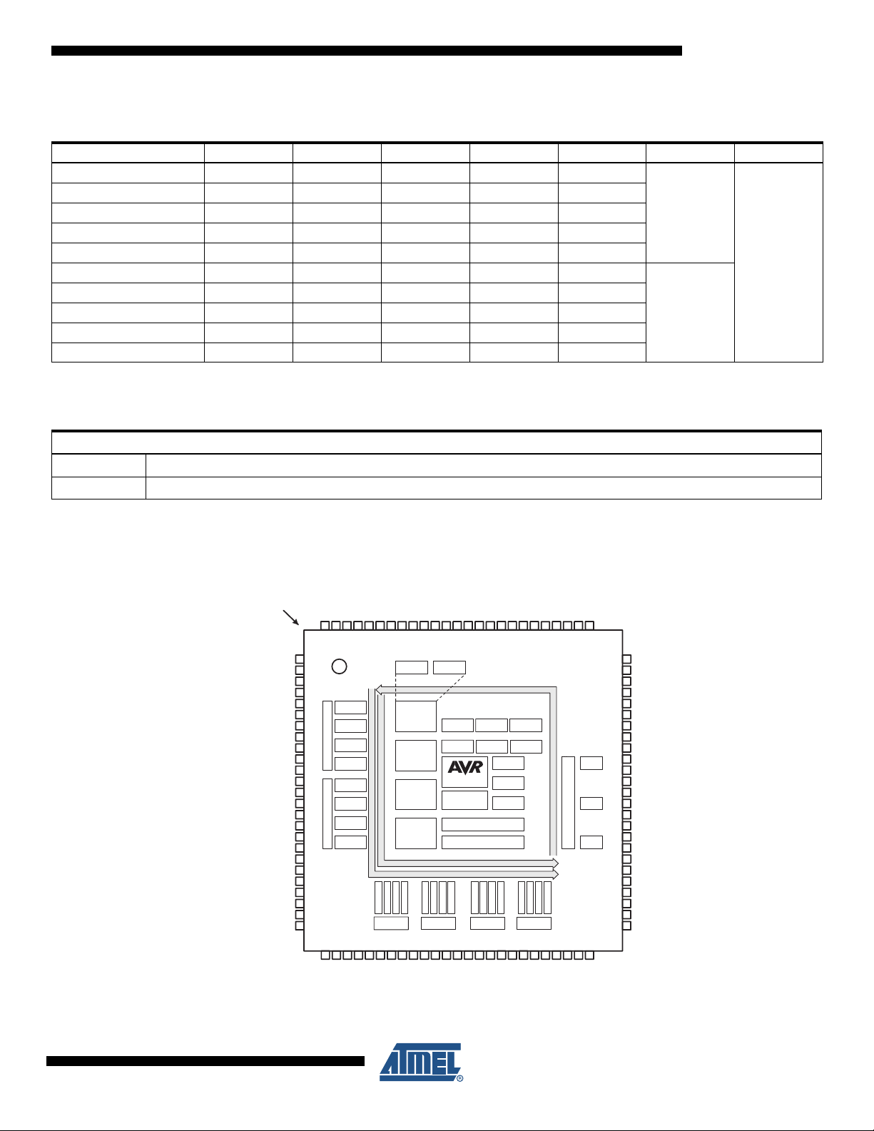
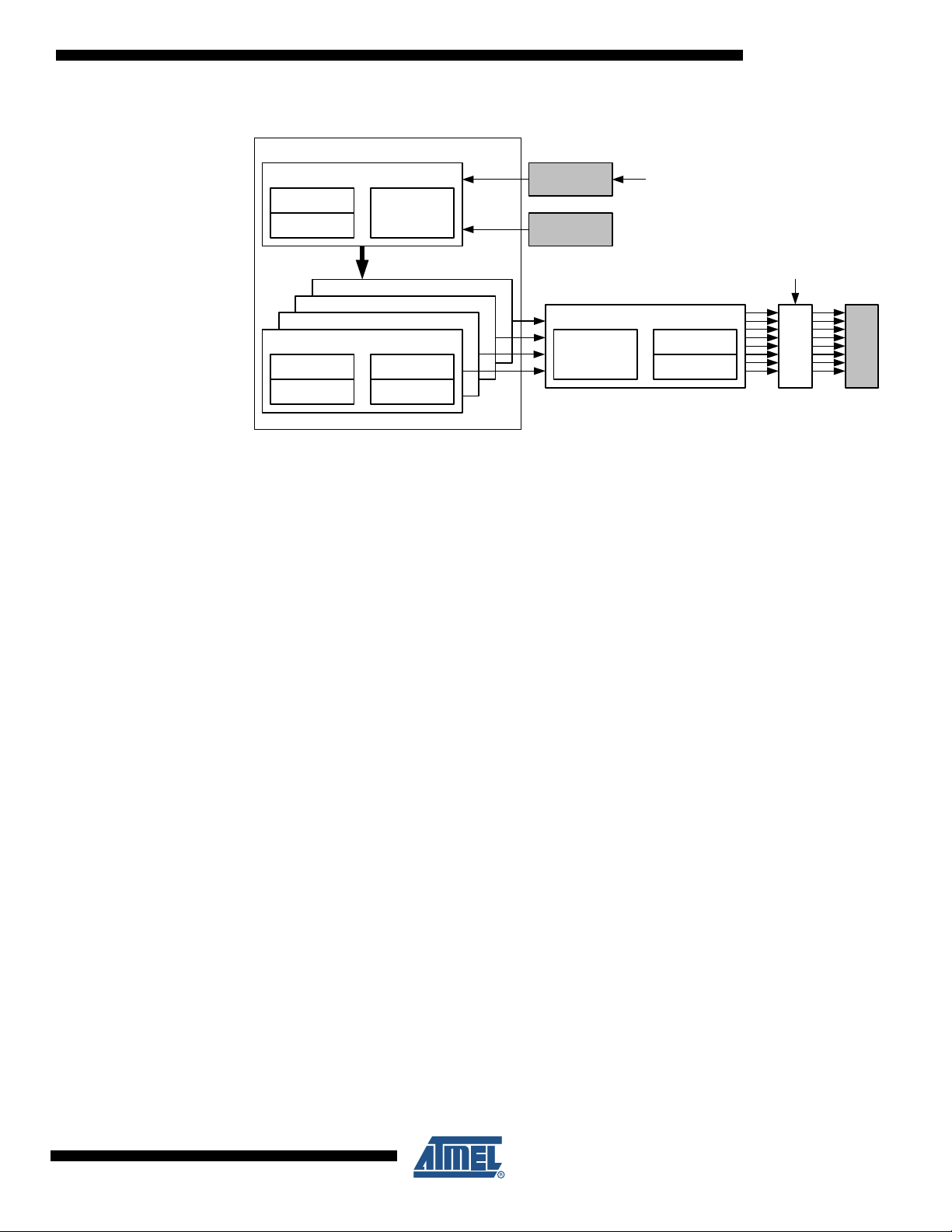
2. Pinout/Block Diagram
100A
100C1
(1)(2)(3)
Temp
-40° - 85°C
Figure 2-1. Block diagr am and T QF P -p inou t.
INDEX CORNER
PA6
PA7
GND
AVCC
PB0
PB1
PB2
PB3
PB4
PB5
PB6
PB7
GND
VCC
PC0
PC1
PC2
PC3
PC4
PC5
PC6
PC7
GND
VCC
PD0
PA5
PA4
9998979695949392919089888786858483828180797877
100
1
2
3
4
5
ADC A
6
DAC A
7
A
8
Port
AC A0
9
10
AC A1
11
12
ADC B
13
DAC B
14
B
15
Port
AC B0
16
17
AC B1
18
19
20
21
22
23
24
25
26272829303132333435363738394041424344454647484950
PD1
PD2
PA3
PD3
PA2
PD4
PA1
PD5
PA0
T/C0:1
Port C
PD6
AVCC
TWI
USART0:1
PD7
GND
PR1
Port R
OSC/CLK
Contro l
Power
Contro l
Reset
Contro l
Watchdog
SPI
VCC
GND
PR0
RESET/PDI
PDI
PQ3
PQ2
Q
Port
DATA BU
BOD POR
TEMP
CPU
DMA
Interrupt Controlle r
Event System ctrl
DATA BU
EVENT ROUTING NETWORK
TWI
SPI
T/C0:1
PE0
T/C0:1
USART0/1
PE1
PE2
PE3
PE4
PQ1
S
VREF
RTC
S
USART0:1
PE5
PQ0
FLASH
RAM
E2PROM
TWI
SPI
PE6
GND
PE7
VCC
OCD
T/C0:1
Port FPort EPort D
GND
PK7
VCC
PK6
PK5
PK4
PK3
PK2
PK1
76
75
PK0
74
VCC
73
GND
72
PJ7
71
PJ6
70
PJ5
69
PJ4
68
PJ3
67
PJ2
66
Port K
nterface
Port J
External Bus I
Port H
TWI
SPI
USART0:1
PF0
PF1
PF2
PF3
PF4
PF5
PJ1
65
PJ0
64
VCC
63
GND
62
PH7
61
PH6
60
PH5
59
PH4
58
PH3
57
PH2
56
PH1
55
PH0
54
VCC
53
GND
52
PF7
51
PF6
Note: For full details on pinout and pin functions refer to “Pinout and Pin Functions” on page 48.
8067C–AVR–05/08
2
Page 3
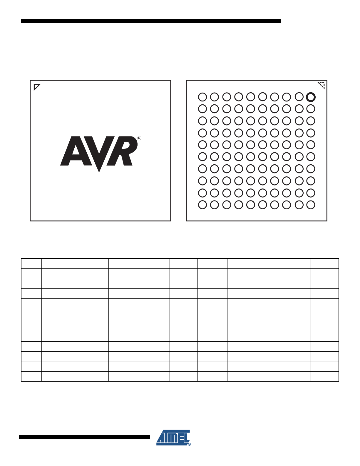
Figure 2-2. CBGA-pinout
A
B
C
D
E
F
G
H
J
K
A
B
C
D
E
F
G
H
J
K
Top view
Bottom view
XMEGA A1
1 2345678910
10987654321
Table 2-1. CBGA-pinout
1 2 3 4 56 78910
A PK0 VCC GND PJ3 GND VCC PH1 GND VCC PF7
B PK3 PK2 PK1 PJ4 PH7 PH4 PH2 PH0 PF6 PF5
C VCC PK5 PK4 PJ5 PJ0 PH5 PH3 PF2 PF3 VCC
D GND PK6 PK7 PJ6 PJ1 PH6 PF0 PF1 PF4 GND
TOSC1/
E
F
G GND PA1 PA4 PB3 PB4 PC1 PC6 PD7 PD6 GND
H AVCC PA2 PA5 PB2 PB5 PC0 PC5 PD5 PD4 PD3
J PA0 PA3 PB0 PB1 PB6 PC3 PC4 PC7 PD2 PD1
K PA6 PA7 GND AVCC PB7 VCC GND VCC GND PD0
PQ0
XTAL1/
PR1
TOSC2/
PQ1
XTAL2/
PR0
.
PQ2 PJ7 PJ2 PE7 PE6 PE5 PE4 PE3
RESET/
PDI_CLK
PDI_DATA PQ3 PC2 PE2 PE1 PE0 VCC
8067C–AVR–05/08
3
Page 4

3. Overview
XMEGA A1
The XMEGA A1 is a family of low power, high performance and peripheral rich CMOS 8/16-bit
microcontrollers based on the AVR
instructions in a single clock cycle, the XMEGA A1 achieves throughputs approaching 1 Million
Instructions Per Second (MIPS) per MHz allowing the system designer to optimize power consumption versus processing speed.
The AVR CPU combines a rich instruction set with 32 general purpose working registers. All the
32 registers are directly connected to the Arithmetic Logic Unit (ALU), allowing two independent
registers to be accessed in one single instruction, executed in one clock cycle. The resulting
architecture is more code efficient while achieving throughputs many times faster than conventional single-accumulator or CISC based microcontrollers.
The XMEGA A1 devices provides the following features: In-System Programmable Flash with
Read-While-Write capabilities, Internal EEPROM and SRAM, four-channel DMA Controller,
eight-channel Event System, Programmable Multi-level Interrupt Controller, 78 general purpose
I/O lines, 16-bit Real Time Counter (RTC), eight flexible 16-bit Timer/Counters with compare
modes and PWM, eight USARTs, four Two Wire Serial Interfaces (TWIs), four Serial Peripheral
Interfaces (SPIs), AES and DES crypto engine, two 8-channel, 12-bit ADCs with optional differential input with programmable gain, two 2-channel, 12-bit DACs, four analog comparators with
window mode, programmable Watchdog Timer with seperate Internal Oscillator, accurate internal oscillators with PLL and prescaler and programmable Brown-Out Detection.
The Program and Debug Interface (PDI), a fast 2-pin interface for programming and debugging,
is available. The devices also have an IEEE std. 1149.1 compliant JTAG test interface, and this
can also be used for On-chip Debug and programming.
®
enhanced RISC architecture. By executing powerful
The XMEGA A1 devices have five software selectable power saving modes. The Idle mode
stops the CPU while allowing the SRAM, DMA Controller, Event System, Interrupt Controller and
all peripherals to continue functioning. The Power-down mode saves the SRAM and register
contents but stops the oscillators, disabling all other functions until the next TWI or pin-change
interrupt, or Reset. In Power-save mode, the asyn chrono us Real Time Counte r continue s to run,
allowing the application to maintain a timer base while the rest of the device is sleeping. In
Standby mode, the Crystal/Resonator Oscillator is kept running while the rest of the device is
sleeping. This allows very fast start-up from external crystal combined with low power consumption. In Extended Standby mode, both the main Oscillator and the Asynchronous Timer continue
to run. To further reduce power consumption, the peripheral clock to each individual peripheral
can optionally be stopped in Active mode and Idle sleep mode.
The device is manufactured using Atmel's high-den sity nonvolat ile memory technolog y. The program Flash memory can be reprogrammed in-system through the PDI or JTAG. A Bootloader
running in the device can use any interface to download th e application program to the Fla sh
memory. The Bootloader software in the Boot Flash section will continue to run while the Application Flash section is updated, providing true Read-While-Write operation. By combining an
8/16-bit RISC CPU with In-System Self-Programmable Flas h, th e Atmel XMEGA A1 is a powerful microcontroller family that provides a highly flexible and cost effective solution for many
embedded applications.
The XMEGA A1 devices is supported with a full suite of program and system development tools
including: C compilers, macro assemblers, program debugger/simulators, programmers, and
evaluation kits.
8067C–AVR–05/08
4
Page 5
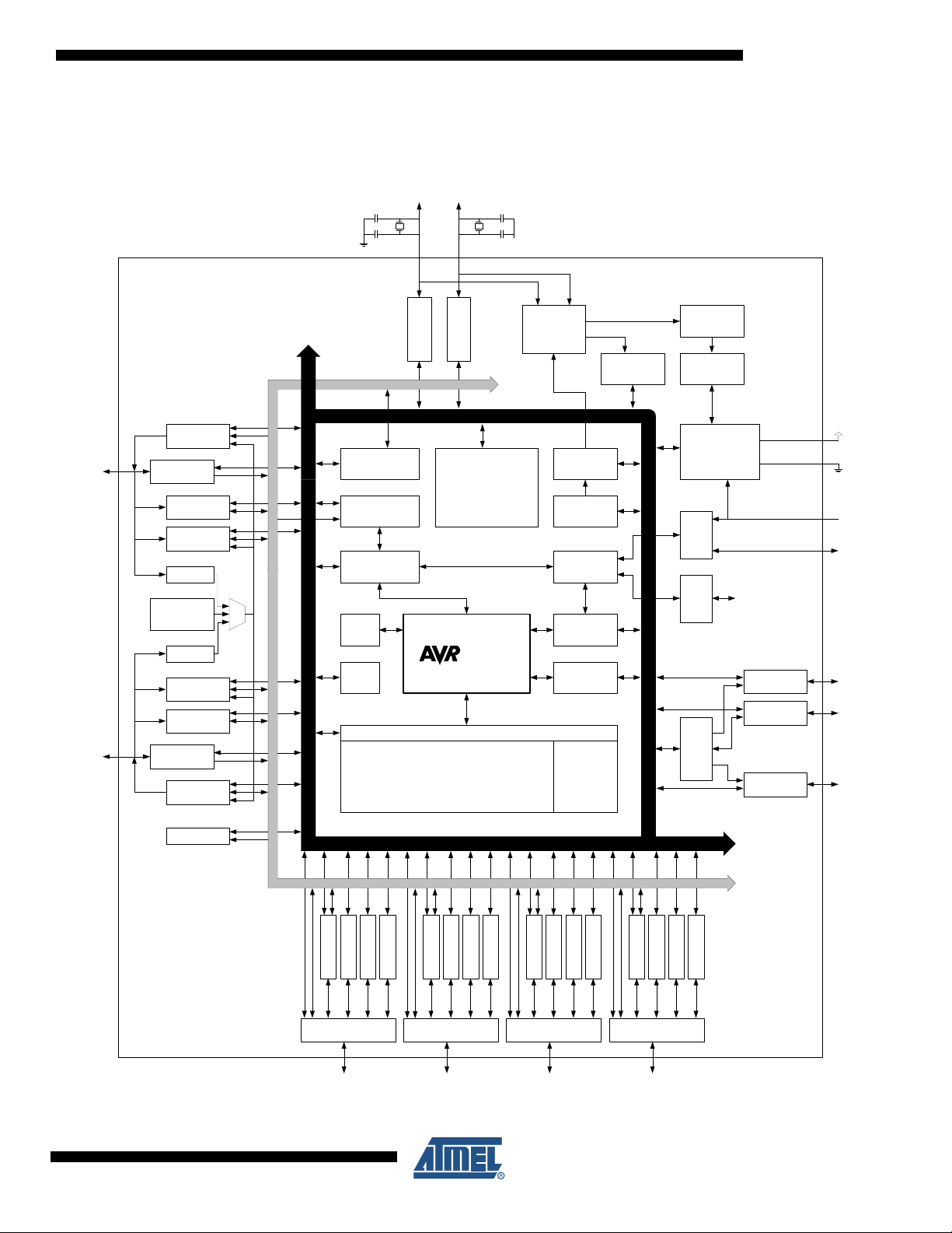
3.1 Block Diagram
Figure 3-1. XMEGA A1 Block Diagram
PR[0..1]
XTAL1
XMEGA A1
PQ[0..3]
TOSC1
PA[0..7]
PB[0..7]/
JTAG
DACA
PORT A (8)
ACA
ADCA
AREFA
Internal
Reference
AREFB
ADCB
ACB
PORT B (8)
DACB
XTAL2
EVENT ROUTING NETWORK
Event System
Controller
DMA
Controller
BUS
Controller
DES
AES
TOSC2
Oscillator
Circuits/
Clock
PORT R (2)
PORT Q (4)
DATA BUS
SRAM
CPU
NVM Controller
Flash EEPROM
Generation
Oscillator
Control
Controller
Prog/Debug
Controller
Interrupt
Controller
Sleep
OCD
Real Time
Counter
Watchdog
Oscillator
Watchdog
Timer
Power
Supervision
POR/BOD &
RESET
PDI
JTAG
EBI
PORT B
PORT K (8)
PORT J (8)
PORT H (8)
VCC
GND
RESET/
PDI_CLK
PDI_DATA
PK[0..7]
PJ[0..7]
PH[0..7]
8067C–AVR–05/08
IRCOM
TCC0:1
USARTC0:1
PORT C (8)
PC[0..7]
SPIC
DATA BUS
EVENT ROUTING NETWORK
TWIC
PORT D (8)
SPID
TCD0:1
PD[0..7] PE[0..7] PF[0..7]
TWID
USARTD0:1
PORT E (8) PORT F (8)
TCE0:1
SPIE
USARTE0:1
TWIE
SPIF
TCF0:1
TWIF
USARTF0:1
5
Page 6

4. Resources
A comprehensive set of development tools, application notes and datasheets are available for
download on http://www.atmel.com/avr.
4.1 Recommended reading
• XMEGA A Manual
• XMEGA A Application Notes
This device data sheet only contains part specific inf ormation and a short de scription of each
peripheral and module. The XMEGA A Manual describes the modules and peripherals in depth.
The XMEGA A application notes contain example code and show applied use of the modules
and peripherals.
The XMEGA A Manual and Application Notes are available from http:// www.atmel.com/avr.
5. Disclaimer
For devices that are not available yet, typical values contained in this datasheet are based on
simulations and characterization of other AVR XMEGA microcontrollers manufactured on the
same process technology. Min. and Max values will be available after the device is
characterized.
XMEGA A1
8067C–AVR–05/08
6
Page 7
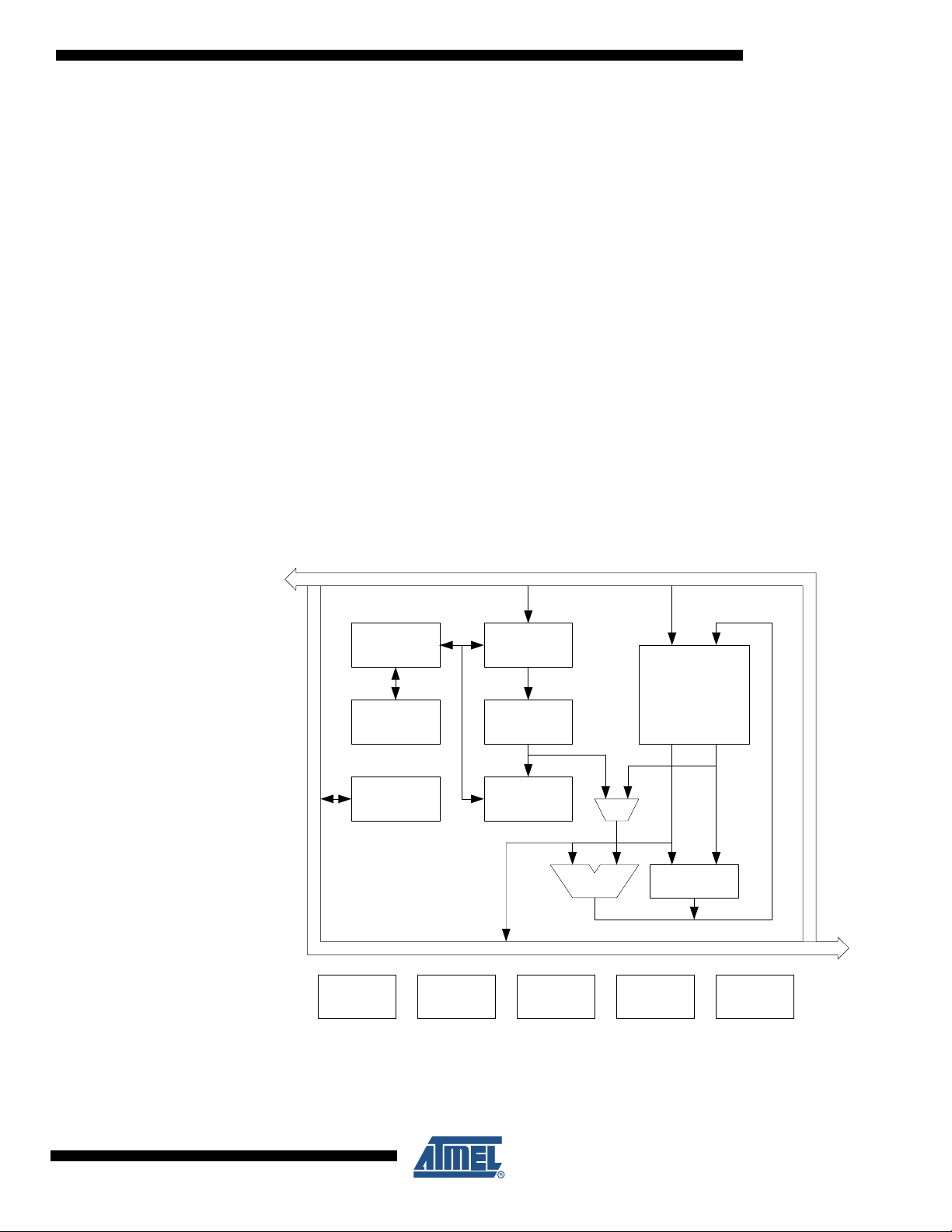
6. AVR CPU
6.1 Features
6.2 Overview
XMEGA A1
• 8/16-bit high performance AVR RISC Architecture
– 138 instructions
– Hardware multiplier
• 32x8-bit registers directly connected to the ALU
• Stack in SRAM
• Stack Pointer accessible in I/O memory space
• Direct addressing of up to 16M Bytes of program and data memory
• True 16/24-bit access to 16/24-bit I/O registers
• Support for 8-, 16- and 32-bit Arithmetic
• Configuration Change Protection of system critical features
The XMEGA A1 uses the 8/16-bit AVR CPU. The main function of the CPU is program exec ution. The CPU must therefore be able to access memories, per form calculations and control
peripherals. Interrupt handling is described in a separate section. Figure 6-1 on page 7 shows
the CPU block diagram.
Figure 6-1. CPU block diagram
Program
Counter
OCD
STATUS/
CONTROL
Peripheral
Module 1
Peripheral
Module 2
DATA BUS
Flash
Program
Memory
Instruction
Register
Instruction
Decode
ALU
DATA BUS
32 x 8 General
Purpose
Registers
Multiplier/
DES
EEPROM PMICSRAM
8067C–AVR–05/08
The AVR uses a Harvard architecture - with separate memories and buses for program and
data. Instructions in the program memory are executed with a single level pipeline. While one
instruction is being executed, the next instruction is pre-fetched from the program memory. This
7
Page 8

concept enables instructions to be executed in every clock cycle. The pr ogram memory is InSystem Self-Programmable Flash memory.
6.3 Register File
The fast-access Register File contains 32 x 8-bit general purpose working registers with single
clock cycle access time. This allows single-cycle Arithmetic Logic Unit (ALU) operation. In a typical ALU cycle, the operation is performed on two Register File operands, and the result is stored
back in the Register File.
Six of the 32 registers can be used as three 16-bit address register pointers for data space
addressing - enabling efficient address calculations. One of these address pointers can also be
used as an address pointer for look up tables in Flash progra m memory.
6.4 ALU - Arithmetic Logic Unit
The high performance Arithmetic Logic Unit (ALU) supports arithmetic and logic operations
between registers or between a constant and a register. Single register operations can also be
executed. Within a single clock cycle, arithmetic operations between general purpose registers
or between a register and an immediate are executed. After an arithmetic or logic operation, the
Status Register is updated to reflect information about the result of the operation.
XMEGA A1
6.5 Program Flow
The ALU operations are divided into three main categories – arithmetic, logical, and bit-functions. Both 8- and 16-bit arithmetic is supported, and the instruction set allows for efficient
implementation of 32-bit aritmetic. The ALU also provides a powerful multiplier supporting both
signed and unsigned multiplication and fractional format.
When the device is powered on, the CPU starts to execute instructions from the lowest address
in the Flash Program Memory ‘0’. The Program Counter (PC) addresses the next instruction to
be fetched. After a reset, the PC is set to location ‘0’.
Program flow is provided by conditional and unconditional jump and call instructions, capable of
addressing the whole address space directly. Most AVR instructions use a 16-bit word format,
while a limited number uses a 32-bit format.
During interrupts and subroutine calls, the return address PC is stored on the Stack. The Stack
is effectively allocated in the general data SRAM, and consequent ly the Stack size is o nly limited
by the total SRAM size and the usage of the SRAM. After reset the Stack Pointer (SP) points to
the highest address in the internal SRAM. The SP is read/write accessib le in the I/O memory
space, enabling easy implementation of multiple stacks or stack areas. The data SRAM can
easily be accessed through the five differe n t addr es s ing mode s su pp or te d in th e A V R CPU.
8067C–AVR–05/08
8
Page 9

7. Memories
7.1 Features
7.2 Overview
XMEGA A1
• Flash Program Memory
– One linear address space
– In-System Programmable
– Self-Programming and Bootloader support
– Application Section fo r application code
– Application Table Section for application code or data storage
– Boot Section for application code or bootloader code
– Separate lock bits and protection for all sections
• Data Memory
– One linear address space
– Single cycle access from CPU
– SRAM
– EEPROM
Byte or page accessible
Optional memory mapping for direct load and store
– I/O Memory
Configuration and Status registers for all peripherals and modules
16-bit accessible General Purpose Register for global variables or flags
– External Memory support
– Bus arbitration
Safe and deterministic handling of CPU and DMA Controller priority
– Separate buses for SRAM, EEPROM, I/O Memory and External Memory access
Simultaneous bus access for CPU and DMA Controller
• Two Signature Row Flash Memories
– Factory programmed data
Oscillator calibration bytes
Serial number
Device ID for each device type
– User programmable memory
One flash page in size
Data is kept after normal chip erase
The AVR architecture has two main memory spaces, the Program Memory and the Data Memory. In addition, the XMEGA A1 features an EEPROM Memory for non-volatile data storage. All
three memory spaces are linear and require no paging. The available memory size configurations are shown in “Ordering Information” on page 2. In addition each device has a Flash
memory signature row for calibration data, device identification, serial number etc.
Non-volatile memory spaces can be locked for further write or read/write operations. This prevents unrestricted access to the application software.
7.3 In-System Programmable Flash Program Memory
The XMEGA A1 devices contains On-chip In-System Programmable Flash memory for program
storage, see Figure 7-1 on page 10. Since all AVR instructions are 16- or 32-bits wide, each
Flash address location is 16 bits.
8067C–AVR–05/08
9
Page 10
XMEGA A1
The Program Flash memory space is divided into Application and Boot sections. Both sections
have dedicated Lock Bits for setting restrictio ns on write or rea d/write ope rations. The Sto re Program Memory (SPM) instruction must reside in the Boot Section when used to write to the Flash
memory.
A third section inside the Application section is referred to as the Application Table section which
has separate Lock bits for storage of write or read/write protection. The Application Table section can be used for storing non-volatile data or application software.
Figure 7-1. Flash Program Memory (Hexadecimal address)
Word Address
0
2EFFF / 1EFFF / 16FFF / EFFF / 77FF
2F000 / 1F000 / 17000 / F000 / 7800
2FFFF / 1FFFF / 17FFF / FFFF / 7FFF
30000 / 20000 / 18000 / 10000 / 8000
30FFF / 20FFF / 18FFF / 10FFF / 87FF
Application Section
(384K/256K/192K/128K/64K)
...
Application Table Section
(8K/8K/8K/8K/4K)
Boot Section
(8K/8K/8K/8K/4K)
The Application Table Section and Boot Section can also be used for general application
software.
7.4 Data Memory
The Data Memory consist of the I/O Memory, EEPROM and SRAM memories, all within one linear address space, see Figure 7-2 on page 10 . To simplify development, the memory map for all
devices in the family is identical and with empty, reserved memory space for smaller devices.
Figure 7-2. Data Memory Map (Hexadecimal address)
Byte Address ATxmega192A1 Byte Address ATxmega128A1 Byte Address ATxmega64A1
1000
17FF 17FF 17FF
2000
5FFF 3FFF 2FFF
6000
FFFFFF FFFFFF FFFFFF
8067C–AVR–05/08
0
FFF FFF FFF
I/O Registers
(4KB)
EEPROM
(2K)
RESERVED RESERVED RESERVED
Internal SRAM
(16K)
External Memory
(0 to 16 MB)
1000
2000
4000
0
I/O Registers
Internal SRAM
Externa l Memory
(0 to 16 MB)
(4KB)
EEPROM
(2K)
(8K)
1000
2000
3000
0
I/O Registers
EEPROM
Internal SRAM
External Memory
(0 to 16 MB)
(4KB)
(2K)
(4K)
10
Page 11
XMEGA A1
Byte Address ATxmega384A1 Byte Address ATxmega256A1
0
I/O Registers
FFF FFF
(4KB)
0
I/O Registers
(4KB)
7.4.1 I/O Memory
1000
EEPROM
(4K)
1FFF 1FFF
2000
9FFF 5FFF
10000
FFFFFF FFFFFF
Internal SRAM
(32K)
External Memory
(0 to 16 MB)
1000
2000
6000
EEPROM
(4K)
Internal SRAM
(16K)
External Memory
(0 to 16 MB)
All peripherals and modules are addressable through I/O memory locations in the data memory
space. All I/O memory locations can be accessed by the Load (LD/LDS/LDD) and Store
(ST/STS/STD) instructions, transferring data between the 32 general purpo se registers in the
CPU and the I/O Memory.
The IN and OUT instructions can address I/O memory locations in the range 0x00 - 0x3F
directly.
I/O registers within the address range 0x00 - 0x1F are directly bit-accessible using the SBI and
CBI instructions. The value of single bits can be checked by using th e SBIS and SBIC instructions on these registers.
The I/O memory address for all peripherals and modules in XMEGA A1 is shown in the “Periph-
eral Module Address Map” on page 54.
7.4.2 SRAM Data Memory
The XMEGA A1 devices has internal SRAM memory for data storage.
7.4.3 EEPROM Data Memory
The XMEGA A1 devices has internal EEPROM mem ory for non-volatile data storage. It is
addressable either in a separate data space or it can be m emory mapped into the normal d ata
memory space. The EEPROM memory supports both byte and page access.
8067C–AVR–05/08
11
Page 12

7.4.4 EBI - External Bus Interface
Supports SRAM up to
•
– 512K Bytes using 2-port EBI
– 16M Bytes using 3-port EBI
• Supports SDRAM up to
– 128M bit using 3-port EBI
• Four software configurable Chip Selects
• Software configurable Wait State insertion
• Clocked from the Peripheral 2x Clock at up to two times the CPU clock speed
The External Bus Interface (EBI) is the interface for connecting external peripheral and memory
to the data memory space. The XMEGA A1 has 3 ports that can be used fo r the EBI. It can in terface external SRAM, SDRAM, and/or peripherals such as LCD displays and other memory
mapped devices..
The address space, and the number of pins used, for the external memory is selectable from
256 bytes (8-bit) and up to 16M bytes (24-bit). Various multiplexing modes for address and data
lines can be selected for optimal use of pins when more or less pins is ava ilab l e for the EB I.
Each of the four chip selects has seperate configuration, and can be configured for SRAM ,
SRAM Low Pin Count (LPC) or SDRAM. The data memory address space associated for each
chip select is decided by a configurable base address and address size for each chip celect.
XMEGA A1
For SDRAM both 4-bit SDRAM is supported, and SDRAM configurations such as CAS Latency
and Refresh rate is configurable in software.
The EBI is clocked from the Peripheral 2x Clock, running up to two times faster than the CPU
and supporting speeds of up to 64 MHz.
8067C–AVR–05/08
12
Page 13
7.5 Signature Rows
The Non Volatile Memory has two sections that are not affected by chip erase. Each section is
one flash page in size, and is used for parameter storage.
One section is for factory programmed device ID, serial number, and calibration data for functions such as the oscillators. The device ID for the available XMEGA A1 devices is shown in
Table 7-1 on page 13. Some of the calibration values will be automatically loaded to the corre-
sponding module or peripheral unit during reset. Th is section can not be erased , and it can be
read from application software and external programming.
Table 7-1. Device ID bytes for XMEGA A1 devices.
XMEGA A1
Device Device ID bytes
Byte 2 Byte 1 Byte 0
ATxmega64A1 4E 96 1E
ATxmega128A1 4C 97 1E
ATxmega192A1 4E 97 1E
ATxmega256A1 46 98 1E
ATxmega384A1 TBD TBD TBD
The other section is fully accessible (read and write) from application software and external
interface programming. This is meant to be used to store data that should not be erased during
chip erase or on-chip debug sessions. This section can only be erased using a dedicated erase
command.
8067C–AVR–05/08
13
Page 14
XMEGA A1
7.6 Flash and EEPROM Page Size
The Flash Program Memory and EEPROM data memory is organized in pages. The pages are
word accessible for the Flash and byte accessible for the EEPROM.
Table 7-2 on page 14 shows the Flash Program Memory organization. Flash write and erase
operations are performed on one page at the time, while reading the Flash is done one byte at
the time. For Flash access the Z-pointer (Z[m:n]) is used for addressing. The most significant
bits in the address (FPAGE) gives the page number and the least significant address bits
(FWORD) gives the word in the page.
Table 7-2. Number of words and Pages in the Flash.
Devices Flash Page Size FWORD FPAGE Application Boot
Size (Bytes) (words) Size No of Pages Size No of Pages
ATxmega64A1 64K + 4K 128 Z[7:1] Z[16:8] 64K 256 4K 16
ATxmega128A1 128K + 8K 256 Z[8:1] Z[17:9] 128K 256 8K 16
ATxmega192A1 192K + 8K 256 Z[8:1] Z[18:9] 192K 384 8K 16
ATxmega256A1 256K + 8K 256 Z[8:1] Z[18:9] 256K 512 8K 16
ATxmega384A1 384K + 8K 256 Z[8:1] Z[19:9] 384K 768 8K 16
Table 7-3 on page 14 shows EEPROM memory organization for the XMEGA A1 devices.
EEPROM write and erase operations can be performed one page or one byte at the time, while
reading the EEPROM is done one byte at the time. For EEPROM access the NVM Address
Register (ADDR[m:n]) is used for addressing. The most significant bits in the address ( E2PAGE)
gives the page number and the least significant address bits (E2BYTE) gives the byte in the
page.
Table 7-3. Number of Bytes and Pages in the EEPROM.
Devices EEPROM Page Size E2BYTE E2PAGE No of Pages
Size (Bytes) (Bytes)
ATxmega64A1 2K 32 ADDR[4:0] ADDR[10:5] 64
ATxmega128A1 2K 32 ADDR[4:0] ADDR[10:5] 64
ATxmega192A1 2K 32 ADDR[4:0] ADDR[10:5] 64
ATxmega256A1 4K 32 ADDR[4:0] ADDR[11:5] 128
ATxmega384A1 4K 32 ADDR[4:0] ADDR[11:5] 128
8067C–AVR–05/08
14
Page 15

8. DMAC - Direct Memory Access Controller
8.1 Features
• Allows High-speed data transfer
– From memory to peripheral
– From memory to memory
– From peripheral to memory
– From peripheral to peripheral
• 4 Channels
• From 1 byte and up to 16M bytes transfers in a single transaction
• Multiple addressing modes for source and destination address
–Increment
– Decrement
– Static
• 1, 2, 4, or 8 byte Burst Transfers
• Programmable priority between channels
8.2 Overview
The XMEGA A1 has a Direct Memory Access (DMA) Controller to move data between memori es
and peripherals in the data space. The DMA controller uses the same data bus as the CPU to
transfer data.
XMEGA A1
It has 4 channels that can be configured independently. Each DMA channel can perform data
transfers in blocks of configurable size from 1 to 64K bytes. A repeat counter can be used to
repeat each block transfer for single transactions up to 16M bytes. Each DMA channel can be
configured to access the source and destination memory a ddress with i ncrementing, d ecrementing or static addressing. The addressing is independent for source and destination address.
When the transaction is complete the original source and destination address can automatically
be reloaded to be ready for the next transaction.
The DMAC can access all the peripherals through thei r I/ O m emory r egist ers, a nd th e DMA m ay
be used for automatic transfer of data to/from communication modules, as well as automatic
data retrieval from ADC conversions, data transfer to DAC conversions, or data transfer to or
from port pins. A wide range of transfer triggers is available from the peripherals, Event System
and software. Each DMA channel has different transfer triggers.
To allow for continuous transfers, two channels can be interlinked so that the second takes over
the transfer when the first is finished and vice versa.
The DMA controller can read from memory mapped EEPROM, but it cannot write to the
EEPROM or access the Flash.
8067C–AVR–05/08
15
Page 16

9. Event System
9.1 Features
9.2 Overview
• Inter-peripheral communication and signalling with minimum latency
• CPU and DMA independent operation
• 8 Event Channels allows for up to 8 signals to be routed at the same time
• Events can be generated by
– Timer/Counters (TCxn)
– Real Time Counter (RTC)
– Analog to Digital Converters (ADCx)
– Analog Comparators (ACx)
– Ports (PORTx)
– System Clock (Clk
– Software (CPU)
SYS
)
• Events can be used by
– Timer/Counters (TCxn)
– Analog to Digital Converters (ADCx)
– Digital to Analog Converters (DACx)
– Ports (PORTx)
– DMA Controller (DMAC)
– IR Communication Module (IRCOM)
• The same event can be used by multiple peripherals for synchronized timing
• Advanced Features
– Manual Event Generation from software (CPU)
– Quadrature Decoding
– Digital Filtering
• Functions in Active and Idle mode
XMEGA A1
8067C–AVR–05/08
The Event System is a set of features for inter-peripheral communication. It enab les the possibility for a change of state in one peripheral to automatically trigger actions in one or more
peripherals. What changes in a peripheral that will trigger actions in other peripherals are configurable by software. It is a simple, but powerful system as it allows for autonomous control of
peripherals without any use of interrupts, CPU or DMA resources.
The indication of a change in a peripheral is referred to as an event, and is usually the same as
the interrupt conditions for that peripheral. Events are passed between peripherals using a dedicated routing network called the Event Routing Network. Figure 9-1 on page 17 shows a basic
block diagram of the Event System with the Event Routin g Networ k an d the pe ripher als t o wh ich
it is connected. This highly flexible system can be used for simple routing of signals, pin functions or for sequencing of events.
The maximum latency is two CPU clock cycles from when an event is generated in one peripheral, until the actions are triggered in one or more other peripherals.
The Event System is functional in both Active and Idle modes.
16
Page 17
Figure 9-1. Event system block diagram.
XMEGA A1
PORTx
ADCx
ClkSYS
CPU
RTC
Event Routing
Network
DACx
ACx
DMACIRCOM
T/Cxn
The Event Routing Network can directly connect togethe r ADCs, DACs, Analog Comparators
(ACx), I/O ports (PORTx), the Real-time Counter (RTC), Timer/Counters (T/C) and the IR Communication Module (IRCOM). Events can also be generated from software (CPU).
All events from all peripherals are always ro ut ed into th e Eve nt Rou tin g Netw or k. T his con sist of
eight multiplexers where each can be configured in software to select which event to be routed
into that event channel. All eight event channels are connected to the peripherals that can use
events, and each of these peripherals can be configured to use events from one or more event
channels to automatically trigger a software selectable action.
8067C–AVR–05/08
17
Page 18

10. System Clock and Clock options
10.1 Features
• Fast start-up time
• Safe run-time clock switching
• Internal Oscillators:
– 32 MHz run-time calibrated RC oscillator
– 2 MHz run-time calibrated RC oscillator
– 32 kHz calibrated RC oscillator
– 32 kHz Ultra Low Power (ULP) oscillator
• External clock options
– 0.4 - 16 MHz Crystal Oscillator
– 32 kHz Crystal Oscillator
– External clock
• PLL with internal and external clock options with 2 to 31x multiplication
• Clock Prescalers with 2 to 2048x division
• Fast peripheral clock running at 2 and 4 times the CPU clock speed
• Automatic Run-Time Calibration of internal oscillators
• Crystal Oscillator failure detection
10.2 Overview
XMEGA A1
XMEGA A1 has an advanced clock system, supporting a lar ge numbe r of clo ck sources. It in corporates both integrated oscillators, external crystal oscillators and resonators. A high frequency
Phase Locked Loop (PLL) and clock prescalers can be controlled from software to generate a
wide range of clock frequencies from the clock source input.
It is possible to switch between clock sources from software during run-time. After reset the
device will always start up running from the 2 Mhz internal oscillator.
A calibration feature is available, and can be used for automatic run-time calibration of the internal 2 MHz and 32 MHz oscillators. This reduce frequency drift over voltage and temperature.
A Crystal Oscillator Failure Monitor can be enabled to issue a Non-Maskable Interrupt and
switch to internal oscillator if the external oscillator fails. Figure 10-1 on page 19 shows the principal clock system in XMEGA A1.
8067C–AVR–05/08
18
Page 19
Figure 10-1. Clock system overview
32 kHz ULP
Internal Oscillator
32.768 kHz
Calibrated Internal
Oscillator
clk
clk
XMEGA A1
ULP
WDT/BOD
RTC
RTC
2 MHz
Run-Time Calibrated
Internal Oscillator
32 MHz
Run-time Calibrated
Internal Oscillator
32.768 KHz
Crystal Oscillator
0.4 - 16 MHz
Crystal Oscillator
External
Clock Input
CLOCK CONTROL
UNIT
with PLL and
Prescaler
clk
clk
PERIPHERALS
PER
INTERRUPT
NVM MEMORY
CPU
ADC
DAC
PORTS
...
DMA
EVSYS
RAM
CPU
FLASH
EEPROM
Each clock source is briefly described in the following sub-sections.
10.3 Clock Options
10.3.1 32 kHz Ultra Low Power Internal Oscillator
The 32 kHz Ultra Low Power (ULP) Internal Oscillator is a very low power consumptio n clock
source. It is used for the Watchdog Timer, Brown-Out Detection and as an asynchronous clock
source for the Real Time Counter. This oscillator cannot be used as the system clock source,
and it cannot be directly controlled from software.
10.3.2 32.768 kHz Calibrated Internal Oscillator
The 32.768 kHz Calibrated Internal Oscillator is a high accuracy clock source that can be used
as the system clock source or as an asynchronous clock source for the Real Time Counter. It is
calibrated during protection to provide a default frequency which is close to its nominal
frequency.
8067C–AVR–05/08
19
Page 20

10.3.3 32.768 kHz Crystal Oscillator
The 32.768 kHz Crystal Oscillator is a low power driver for an external watch crystal. It can be
used as system clock source or as asynchronous clock source for the Real Time Counter.
10.3.4 0.4 - 16 MHz Crystal Oscillator
The 0.4 - 16 MHz Crystal Oscillator is a driver intended for driving both external resonators and
crystals ranging from 400 kHz to 16 MHz.
10.3.5 2 MHz Run-time Calibrated Internal Oscillator
The 2 MHz Run-time Calibrated Internal Oscillator is a high frequency oscillator. It is calibrated
during protection to provide a default frequency which is close to its nominal frequency. The
oscillator can use the 32 kHz Calibrated Internal Oscillator or the 32 kHz Crystal Oscillator as a
source for calibrating the frequency run-time to compensate for temperature and voltage drift
hereby optimizing the accuracy of the oscillator.
10.3.6 32 MHz Run-time Calibrated Internal Oscillator
The 32 MHz Run-time Calibrated Internal Oscillator is a high frequency oscillator. It is calibrated
during protection to provide a default frequency which is close to its nominal frequency. The
oscillator can use the 32 kHz Calibrated Internal Oscillator or the 32 kHz Crystal Oscillator as a
source for calibrating the frequency run-time to compensate for temperature and voltage drift
hereby optimizing the accuracy of the oscillator.
XMEGA A1
10.3.7 External Clock input
The external clock input gives the possibility to connect a clock from an external source.
10.3.8 PLL with Multiplication factor 2 - 31x
The PLL provides the possibility of multiplying a frequency by any number from 2 to 31. In combination with the prescalers, this gives a wide range of o utput frequencies f rom all clock sources.
8067C–AVR–05/08
20
Page 21

11. Power Management and Sleep Modes
11.1 Features
• 5 sleep modes
–Idle
– Power-down
–Power-save
–Standby
– Extended standby
• Power Reduction registers to disable clocks to unused peripherals
11.2 Overview
The XMEGA A1 provides various sleep modes tailored to reduce power consumption to a minimum. All sleep modes are available and can be entered from Active mode. In Active mode the
CPU is executing application code. The application code decides when and what sleep mode to
enter. Interrupts from enabled peripherals and all enabled reset sources can restore the microcontroller from sleep to Active mode.
In addition, Power Reduction registers provide a method to stop the clock to individual peripherals from software. When this is done, the current state of the peripheral is frozen and there is no
power consumption from that peripheral. This reduces the power consumption in Active mode
and Idle sleep mode.
XMEGA A1
11.3 Sleep Modes
11.3.1 Idle Mode
In Idle mode the CPU and Non-Volatile Memory are stopped, but all peripherals including the
Interrupt Controller, Event System and DMA Controller are kept running. Interrupt requests from
all enabled interrupts will wake the device.
11.3.2 Power-down Mode
In Power-down mode all system clock sources, and the asynchronous Real Time Counter ( RTC)
clock source, are stopped. This allows operation of asynchronous modules only. The only interrupts that can wake up the MCU are the Two Wire Interface address match interrupts, and
asynchronous port interrupts, e.g pin change.
11.3.3 Power-save Mode
Power-save mode is identical to Power-down, with one exception: If the RTC is enable d, it will
keep running during sleep and the device can also wake up from RTC interrupts.
11.3.4 Standby Mode
Standby mode is identical to Power-down with the exception that all enabled system clock
sources are kept running, while the CPU, Peripheral and RTC clocks are stopped. This reduces
the wake-up time when external crystals or resonators are used.
11.3.5 Extended Standby Mode
Extended Standby mode is identical to Power-save mode with the exception that all enabled
system clock sources are kept running while the CPU and Peripheral clocks are stopped. This
reduces the wake-up time when external crystals or resonato rs are used.
8067C–AVR–05/08
21
Page 22

12. System Control and Reset
12.1 Features
• Multiple reset sources for safe operation and device reset
– Power-On Reset
– External Reset
– Watchdog Reset
The Watchdog Timer runs from separate, dedicated oscillator
– Brown-Out Reset
Accurate, programmable Brown-Out levels
– JTAG Reset
– PDI reset
– Software reset
• Asynchronous reset
– No running clock in the device is required for reset
• Reset status register
12.2 Resetting the AVR
During reset, all I/O registers are set to their initial values. The SRAM content is not re se t. Ap plication execution starts from the Reset Vector. The instru ction placed at the Reset Vector should
be an Absolute Jump (JMP) instruction to the reset handling routine. By defau lt t he Reset Vector
address is the lowest Flash program memory address , ‘0’, but it is possible to move the Reset
Vector to the first address in the Boot Section.
XMEGA A1
The I/O ports of the AVR are immediately tri-stated when a reset source goes active.
The reset functionality is asynchronous, so no running clock is require d to reset the device.
After the device is reset, the reset source can be determined by the application by reading the
Reset Status Register.
12.3 Reset Sources
12.3.1 Power-On Reset
The MCU is reset when the supply voltage VCC is below the Power-on Reset threshold voltage.
12.3.2 External Reset
The MCU is reset when a low level is present on the RESET pin.
12.3.3 Watchdog Reset
The MCU is reset when the Watchdog Timer period exp ires and the Wat chdog Reset is enable d.
The Watchdog Timer runs from a dedicated oscillator independen t of the System Clock. For
more details see “WDT - Watchdog Timer” on page 23.
12.3.4 Brown-Out Reset
The MCU is reset when the supply voltage VCC is below the Brown-Out Reset threshold voltage
and the Brown-out Detector is enabled. The Brown-out threshold voltage is programmable.
8067C–AVR–05/08
22
Page 23

12.3.5 JTAG reset
The MCU is reset as long as there is a logic one in the Reset Register in one of the scan chains
of the JTAG system. Refer to IEEE 1149.1 (JTAG) Boundary-scan for details.
12.3.6 PDI reset
The MCU can be reset through the Program and Debug Interface (PDI).
12.3.7 Software reset
The MCU can be reset by the CPU writing to a special I/O register through a timed sequence.
12.4 WDT - Watchdog Timer
12.4.1 Features
11 selectable timeout periods, from 8 ms to 8s.
•
• Two operation modes
– Standard mode
– Window mode
• Runs from the 1 kHz output of the 32 kHz Ultra Low Power oscillator
• Configuration lock to prevent unwanted changes
12.4.2 Overview
XMEGA A1
The XMEGA A1 has a Watchdog Timer (WDT). The WDT will run continuously when turned on
and if the Watchdog Timer is not reset within a software configurable time-out period, the microcontroller will be reset. The Watchdog Reset (WDR) instruction must be run by software to reset
the WDT, and prevent microcontroller reset.
The WDT has a Window mode. In this mode the WDR instruction must be run within a specified
period called a window. Application software can set the minimum and maximum limits for this
window. If the WDR instruction is not executed inside the window limits, the microcontroller will
be reset.
A protection mechanism using a timed write sequence is implemented in order to prevent
unwanted enabling, disabling or change of WDT settings.
For maximum safety, the WDT also has an Always-on mode. This mode is enabled by programming a fuse. In Always-on mode, application software can not disable t he WDT.
8067C–AVR–05/08
23
Page 24

13. PMIC - Programmable Multi-level Interrupt Controller
13.1 Features
• Separate interrupt vector for each interrupt
• Short, predictable interrupt response time
• Programmable Multi-level Interrupt Controller
– 3 programmable interrupt levels
– Selectable priority scheme within low level interrupts (round-robin or fixed)
– Non-Maskable Interrupts (NMI)
• Interrupt vectors can be moved to the start of the Boot Section
13.2 Overview
XMEGA A1 has a Programmable Multi-level Interrupt Controller (PMIC). All peripherals can
define three different priority levels for interrupts; high, medium or low. Medium level interrupts
may interrupt low level interrupt service routines. High level interrupts may interrupt both lowand medium level interrupt service routines. Low level interrupts have an optional round robin
scheme to make sure all interrupts are serviced within a certain amount of time.
The built in oscillator failure detection mechanism can issue a Non-Maskable Interrupt (NMI).
XMEGA A1
13.3 Interrupt vectors
When an interrupt is serviced, the program counter will jump to the interrupt vector address. The
interrupt vector is the sum of the peripheral’s base interrupt address a nd the offset address for
specific interrupts in each peripheral. The base addresses for the XMEGA A1 devices are shown
in Table 13-1. Offset addresses for each interrupt available in the peripheral are described for
each peripheral in the XMEGA A manual. For peripherals or modules that have only one interrupt, the interrupt vector is shown in Table 13-1. The program address is the word address.
Table 13-1. Reset and Interrupt Vectors
Program Address
(Base Address) Source Interrupt Description
0x000 RESET
0x002 OSCF_INT_vect Crystal Oscillator Failure Interrupt vector (NMI)
0x004 PORTC_INT_base Port C Interrupt base
0x008 PORTR_INT_base Port R Interrupt base
0x00C DMA_INT_base DMA Controller Interrupt base
0x014 RTC_INT_base Real Time Counter Interrupt base
0x018 TWIC_INT_base Two-Wire Interface on Port C Interrupt base
0x01C TCC0_INT_base Timer/Counter 0 on port C Interrupt base
0x028 TCC1_INT_base Timer/Counter 1 on port C Interrupt base
0x030 SPIC_INT_vect SPI on port C Interrupt vector
0x032 USARTC0_INT_base USART 0 on port C Interrupt base
0x038 USARTC1_INT_base USART 1 on port C Interrupt base
0x03E AES_INT_vect AES Interrupt vector
8067C–AVR–05/08
24
Page 25

Table 13-1. Reset and Interrupt Vectors (Continued)
Program Address
(Base Address) Source Interrupt Description
0x040 NVM_INT_base Non-Volatile Memory Interrupt base
0x044 PORTB_INT_base Port B Interrupt base
0x048 ACB_INT_base Analog Comparator on Port B Interrupt base
0x04E ADCB_INT_base Analog to Digital Converter on Port B Interrupt base
0x056 PORTE_INT_base Port E Interrupt base
0x05A TWIE_INT_base Two-Wire Interface on Port E Interrupt base
0x05E TCE0_INT_base Timer/Counter 0 on port E Interrupt base
0x06A TCE1_INT_base Timer/Counter 1 on port E Interrupt base
0x072 SPIE_INT_vect SPI on port E Interrupt vector
0x074 USARTE0_INT_base USART 0 on port E Interrupt base
0x07A USARTE1_INT_base USART 1 on port E Interrupt base
0x080 PORTD_INT_base Port D Interrupt base
0x084 PORTA_INT_base Port A Interrupt base
0x088 ACA_INT_base Analog Comparator on Port A Interrupt base
0x08E ADCA_INT_base Analog to Digital Converter on Port A Interrupt base
XMEGA A1
0x096 TWID_INT_base Two-Wire Interface on Port D Interrupt base
0x09A TCD0_INT_base Timer/Counter 0 on port D Interr upt base
0x0A6 TCD1_INT_base Timer/Counter 1 on port D Interr upt base
0x0AE SPID_INT_vector SPI on port D Interrupt vector
0x0B0 USARTD0_INT_base USART 0 on port D Interrupt base
0x0B6 USARTD1_INT_base USART 1 on port D Interrupt base
0x0BC PORTQ_INT_base Port Q INT base
0x0C0 PORTH_INT_base Port H INT base
0x0C4 PORTJ_INT_base Port J INT base
0x0C8 PORTK_INT_base P ort K INT base
0x0D0 PORTF_INT_base Port F INT base
0x0D4 TWIF_INT_base Two-Wire Interface on Port F INT base
0x0D8 TCF0_INT_base Timer/Counter 0 on port F Interrupt base
0x0E4 TCF1_INT_base Timer/Co unter 1 on port F Interrupt base
0x0EC SPIF_INT_vector SPI ion port F Interrupt base
0x0EE USARTF0_INT_base USART 0 on port F Interrupt base
0x0F4 USARTF1_INT_base USART 1 on port F Interrupt base
8067C–AVR–05/08
25
Page 26

14. I/O Ports
14.1 Features
14.2 Overview
XMEGA A1
• Selectable input and output configuration for each pin indi vidually
• Flexible pin configuration through dedicated Pin Configuration Register
• Synchronous and/or asynchronous input sensing with port interrupts and events
– Sense both edges
– Sense rising edges
– Sense falling edges
– Sense low level
• Asynchronous wake-up from all input sensing configurations
• Two port interrupts with flexible pin masking
• Highly configurable output driver and pull settings:
– Totem-pole
– Pull-up/-down
– Wired-AND
– Wired-OR
– Bus-keeper
– Inverted I/O
• Optional Slew rate control
• Configuration of multiple pins in a single operation
• Read-Modify-Write (RMW) support
• Toggle/clear/set registers for Output and Direction registers
• Clock output on port pin
• Event Channel 7 output on port pin
• Mapping of port registers (virtual ports) into bit accessible I/O memory space
The XMEGA A1 devices have flexible General Purpose I/O Ports. A port consists of up to 8 pins,
ranging from pin 0 to pin 7. The ports implement several functions, including synchronous/asynchronous input sensing, pin change interrupts and configurable output settings. All functions are
individual per pin, but several pins may be configured in a single operation.
14.3 I/O configuration
All port pins (Pn) have programmable output configuration. In addition, all port pins have an
inverted I/O function. For an input, this means inverting the signal between the port pin and the
pin register. For an output, this means inverting the output signal between the port register and
the port pin. The inverted I/O function can be used also when the pin is used for alternate functions. The port pins also have configurable slew rate limitation to reduce electromagnetic
emission.
8067C–AVR–05/08
26
Page 27
14.3.1 Push-pull
XMEGA A1
Figure 14-1. I/O configuration - Totem-pole
DIRn
14.3.2 Pull-down
14.3.3 Pull-up
OUTn
INn
Figure 14-2. I/O configuration - Totem-pole with pull-down (on input)
DIRn
OUTn
INn
Pn
Pn
14.3.4 Bus-keeper
8067C–AVR–05/08
Figure 14-3. I/O configuration - Totem-pole with pull-up (on input)
DIRn
OUTn
Pn
INn
The bus-keeper’s weak output produces the same logical level as the last output level. It acts as
a pull-up if the last level was ‘1’, and pull-down if the last level was ‘0’.
27
Page 28

Figure 14-4. I/O configuration - Totem-pole with bus-keeper
DIRn
XMEGA A1
14.3.5 Others
OUTn
Pn
INn
Figure 14-5. Output configuration - Wired-OR with optional pull-down
OUTn
Pn
INn
Figure 14-6. I/O configuration - Wired-AND with optional pull-up
8067C–AVR–05/08
INn
Pn
OUTn
28
Page 29
14.4 Input sensing
XMEGA A1
• Sense both edges
• Sense rising edges
• Sense falling edges
• Sense low level
Input sensing is synchronous or asynchronous depending on the enabled clock for the ports,
and the configuration is shown in Figure 14-7 on page 29.
Figure 14-7. Input sensing system overview
Asynchronous sen sing
Pn
IN V ERT E D I/O
When a pin is configured with inverted I/O the pin value is inverted before the input sensing.
14.5 Port Interrupt
Each ports have two interrupts with seperate priorit y and interrup t vector. All pins on the port can
be individually selected as source for each of the interrupts. The in terrupts are then triggered
according to the input sense configuration for each pin configured as source for the interrupt.
14.6 Alternate Port Functions
In addition to the input/output functions on all port pins, most pins have alternate functions. This
means that other modules or peripherals connected to the port can use the port pins for their
functions, such as communication or pulse-width modulation. “Pinout and Pin Functions” on
page 48 shows which modules on peripherals that enables alternate functions on a pin, and
what alternate functions that is available on a pin.
Synchronizer
INn
Q
Q
D
D
R
R
EDGE
DETECT
Synchronous sen sing
EDGE
DETECT
Interrupt
Control
IR E Q
Event
8067C–AVR–05/08
29
Page 30

15. T/C - 16-bit Timer/Counter
15.1 Features
• Eight 16-bit Timer/Counters
– Four Timer/Counters of type 0
– Four Timer/Counters of type 1
• Four Compare or Capture (CC) Channels in Timer/Counter 0
• Two Compare or Capture (CC) Channels in Timer/Counter 1
• Double Buffered Timer Period Setting
• Double Buffered Compare or Capture Channels
• Waveform Generation:
– Single Slope Pulse Width Modulation
– Dual Slope Pulse Width Modulation
– Frequency Generation
• Input Capture:
– Input Capture with Noise Cancelling
– Frequency capture
– Pulse width capture
– 32-bit input capture
• Event Counter with Direction Control
• Timer Overflow and Timer Error Interrupts and Events
• One Compare Match or Capture Interrupt and Event per CC Channel
• Supports DMA Operation
• Hi-Resolution Extension (Hi-Res)
• Advanced Waveform Extension (AWEX)
XMEGA A1
15.2 Overview
XMEGA A1 has eight Timer/Counters, four Timer/Counter 0 and four Timer/Counter 1. The difference between them is that Timer/Counter 0 has four Compare/Capture channels, while
Timer/Counter 1 has two Compare/Capture channels.
The Timer/Counters (T/C) are 16-bit and can count any clock, event or external input in the
microcontroller. A programmable prescaler is available to get a useful T/C reso lution. Upd ates of
Timer and Compare registers are double buffered to ensure glitch free operation. Single slope
PWM, dual slope PWM and frequency generation waveforms can be generated using the Compare Channels.
Through the Event System, any input pin or event in the microcontroller can be used to trigger
input capture, hence no dedicated pins is requir ed for th is. The input capt ure has a noise canceller to avoid incorrect capture of the T/C, and can be used to do frequency and pulse width
measurements.
A wide range of interrupt or event sources are available, including T/C Overflow, Compare
match and Capture for each Compare/Capture ch annel in the T/C.
PORTC, PORTD, PORTE and PORTF each has one Timer/Counter 0 and one Timer/Counter1.
Notation of these Timer/Counters are TCC0 (Time/Counter C0), TCC1, TCD0, TCD1, TCE0,
TCE1, TCF0, and TCF1, respectively.
8067C–AVR–05/08
30
Page 31
XMEGA A1
Figure 15-1. Overview of a Timer/Counter and closely related peripherals
Timer/Counter
Base Counter
Timer Period
Counter
Control Logic
Compare/Capture Channel D
Compare/Capture Channel C
Compare/Capture Channel B
Compare/Capture Ch a nnel A
Comparator
Buffer
Capture
Control
Waveform
Generation
The Hi-Resolution Extension can be enabled to increase the waveform generation resolution by
2 bits (4x). This is available for all Timer/Counters. See “Hi-Res - High Resolution Extension” on
page 33 for more details.
Prescaler
Event
System
AWeX
DTI
Dead-Time
Insertion
clk
PER
Generation
Protection
Pattern
Fault
clk
PER4
Hi-Res
PORT
The Advanced Waveform Extension can be enabled to provide extra and more advanced features for the Timer/Counter. This are only availa ble for Timer/Cou nter 0. See “AWEX - Advanced
Waveform Extension” on page 32 for more details.
8067C–AVR–05/08
31
Page 32

16. AWEX - Advanced Waveform Extension
16.1 Features
• Output with complementary output from each Capture channel
• Four Dead Time Insertion (DTI) Units, one for each Capture channel
• 8-bit DTI Resolution
• Separate High and Low Side Dead-Time Setting
• Double Buffered Dead-Time
• Event Controlled Fault Protection
• Single Channel Multiple Output Operation (for BLDC motor co ntrol)
• Double Buffered Pattern Generation
16.2 Overview
The Advanced Waveform Extension (AWEX) provides extra features to the Timer/Counter in
Waveform Generation (WG) modes. The AWEX enables easy and safe implementation of for
example, advanced motor control (AC, BLDC, SR, and Stepper) and power control applications.
Any WG output from a Timer/Counter 0 is split into a complimentary pair of outputs when any
AWEX feature is enabled. These output pairs go through a Dead-Time Inse rtion (DTI) unit that
enables generation of the non-inverted Low Side (LS) and inverted High Side (HS) of the WG
output with dead time insertion between LS and HS switching. The DTI outp ut will override the
normal port value according to the port override setting. Optionally the final output can be
inverted by using the invert I/O setting for the port pin.
XMEGA A1
The Pattern Generation unit can be used to generate a synchronized bit pattern on the port it is
connected to. In addition, the waveform generator output from Compare Channel A can be distributed to, and override all port pins. When the Patter n Generat or unit is enabled, the DT I unit is
bypassed.
The Fault Protection unit is connected to the Event System. This enables any event to trigger a
fault condition that will disable the AWEX output. Several event channels can be used to trigger
fault on several different conditions.
The AWEX is available for TCC0 and TCE0. The notation of these peripherals are AWEXC and
AWEXE.
8067C–AVR–05/08
32
Page 33

17. Hi-Res - High Resolution Extension
17.1 Features
• Increases Waveform Generator resolution by 2-bits (4x)
• Supports Frequency, single- and dual-slope PWM operation
• Supports the AWEX when this is enabled and used for the same Timer/Counter
17.2 Overview
The Hi-Resolution (Hi-Res) Extension is able to increase the resolution of t he wavefor m gener ation output by a factor of 4. When enabled for a Timer/Coun ter, the Fast Peri pheral clock running
at four times the CPU clock speed will be as input to the Timer/Counter.
The High Resolution Extension can also be used when an AWEX is enabled and used with a
Timer/Counter.
XMEGA A1 devices have four Hi-Res Extensions that each can be enabled for each
Timer/Counters pair on PORTC, PORTD, PORTE and PORTF. The notation of these peripherals are HIRESC, HIRESD, HIRESE and HIRESF, respectively.
XMEGA A1
8067C–AVR–05/08
33
Page 34

18. RTC - 16-bit Real-Time Counter
18.1 Features
• 16-bit Timer
• Flexible Tick resolution ranging from 1 Hz to 32.768 kHz
• One Compare register
• One Period register
• Clear timer on Overflow or Compare Match
• Overflow or Compare Match event and interrupt generation
18.2 Overview
The XMEGA A1 includes a 16-bit Real-time Counter (RTC). The RTC can be clocked from an
accurate 32.768 kHz Crystal Oscillator, the 32.768 kHz Calibrated Internal Oscillator, or from the
32 kHz Ultra Low Power Internal Oscillator. The RTC includes both a Period and a Compare
register. For details, see Figure 18-1.
A wide range of Resolution and Time-out periods can be conf igure d usin g the RTC. With a maximum resolution of 30.5 µs, time-out periods range up to 2000 seconds. With a resolution of 1
second, the maximum time-out period is over 18 hours (65536 seconds).
XMEGA A1
Figure 18-1. Real Time Counter overview
32 kHz
10-bit
prescaler
1 kHz
Period
Overflow
=
Counter
=
Compare Match
Compare
8067C–AVR–05/08
34
Page 35

19. TWI - Two-Wire Interface
19.1 Features
• Four Identical TWI peripherals
• Simple yet Powerfu l an d Flexible Communication Interface
• Both Master and Slave Operation Supported
• Device can Operate as Transmitter or Receiver
• 7-bit Address Space Allows up to 128 Different Slave Addresses
• Multi-master Arbitration Support
• Up to 400 kHz Data Transfer Speed
• Slew-rate Limited Output Drivers
• Noise Suppression Circuitry Rejects Spikes on Bus Lines
• Fully Programmable Slave Address with General Call Support
• Address Recognition Causes Wake-up when in Sleep Mode
2
• I
C and System Management Bus (SMBus) compatible
19.2 Overview
The Two-Wire Interface (TWI) is a bi-direct ional wired-AND bus with only two lines, the clock
(SCL) line and the data (SDA) line. The protocol makes it possible to interconnect up to 128 individually addressable devices. Since it is a multi-master bus, one or more devices capable of
taking control of the bus can be connected.
XMEGA A1
The only external hardware needed to implement the bus is a single pull-up resistor for each of
the TWI bus lines. Mechanisms for resolving bus contention are inherent in the TWI protocol.
PORTC, PORTD, PORTE, and PORTF each has one TWI. Notation of these peripherals are
TWIC, TWID, TWIE, and TWIF, respectively.
8067C–AVR–05/08
35
Page 36

20. SPI - Serial Peripheral Interface
20.1 Features
• Four Identical SPI peripherals
• Full-duplex, Three-wire Synchronous Data Transfer
• Master or Slave Operation
• LSB First or MSB First Data Transfer
• Seven Programmable Bit Rates
• End of Transmission Interrupt Flag
• Write Collision Flag Protection
• Wake-up from Idle Mode
• Double Speed (CK/2) Master SPI Mode
20.2 Overview
The Serial Peripheral Interface (SPI) allows high-speed full-duplex, synchronous data transfer
between different devices. Devices can communicate using a master-slave scheme, and data is
transferred both to and from the devices simultaneously.
PORTC, PORTD, PORTE, and PORTF each has one SPI. Notation of these peripherals are
SPIC, SPID, SPIE, and SPIF, respectively.
XMEGA A1
8067C–AVR–05/08
36
Page 37

21. USART
21.1 Features
21.2 Overview
XMEGA A1
• Eight Identical USART peripherals
• Full Duplex Operation (Independent Serial Receive and Transmit Registers)
• Asynchronous or Synchronous Operation
• Master or Slave Clocked Synchronous Operation
• High-resolution Arithmetic Baud Rate Generator
• Supports Serial Frames with 5, 6, 7, 8, or 9 Data Bits and 1 or 2 Stop Bits
• Odd or Even Parity Generation and Parity Check Supported by Hardware
• Data OverRun Detection
• Framing Error Detection
• Noise Filtering Includes False Start Bit Detection and Digital Low Pass Filter
• Three Separate Interrupts on TX Complete, TX Data Register Empty and RX Complete
• Multi-processor Communicat ion Mode
• Double Speed Asynchronous Communication Mode
• Master SPI mode for SPI communication
• IrDA support through the IRCOM module
The Universal Synchronous and Asynchronous serial Receive r and Transmitter (USART) is a
highly flexible serial communication module. The USART supports full duplex communication,
and both asynchronous and clocked synchronous operation. The USART can also be set in
Master SPI mode to be used for SPI communication.
Communication is frame based, and the frame format can be customized to support a wide
range of standards. The USART is buffered in both direction, enabling continued data transmission without any delay between frames. There are separate interrupt vectors for receive and
transmit complete, enabling fully interrupt driven communication. Frame error and buffer overflow are detected in hardware and indicated with separate status flags. Even or odd parity
generation and parity check can also be enabled.
One USART can use the IRCOM module to support IrDA 1.4 physical compliant pulse modulation and demodulation for baud rates up to 115.2 kbps.
PORTC, PORTD, PORTE, and PORTF each has two USARTs. Notation of these peripherals
are USARTC0, USARTC1, USARTD0, USARTD1, USARTE0, USARTE1, USARTF0,
USARTF1, respectively.
8067C–AVR–05/08
37
Page 38

22. IRCOM - IR Communication Module
22.1 Features
• Pulse modulation/demodulation for infrared communication
• Compatible to IrDA 1.4 physical for baud rates up to 115.2 kbps
• Selectable pulse modulation scheme
– 3/16 of baud rate period
– Fixed pulse period, 8-bit programmable
– Pulse modulation disabled
• Built in filtering
• Can be connected to and used by one USART at the time
22.2 Overview
XMEGA contains an Infrared Communication Module (IRCOM) for IrDA communication with
baud rates up to 115.2 kbps. This supports three modulat ion sch emes: 3/ 16 of baud rate pe rio d,
fixed programmable pulse time based on the Peripheral Clock speed , or pulse modulation disabled. There is one IRCOM available which can be connected to any USART to enable infrared
pulse coding/decoding for that USART.
XMEGA A1
8067C–AVR–05/08
38
Page 39

23. Crypto Engine
23.1 Features
23.2 Overview
XMEGA A1
• Data Encryption Standard (DES) CPU instruction
• Advanced Encryption Standard (AES) Crypto module
• DES Instruction
– Encryption and Decryption
– Single-cycle DE S instruction
– Encryption/Decryption in 16 clock cycles per 8-byte block
• AES Crypto Module
– Encryption and Decryption
– Support 128-bit keys
– Support XOR data load mode to the State memory for Cipher Block Chaining
– Encryption/Decryption in 375 clock cycles per 16-byte block
The Advanced Encryption Standard (AES) and Data Encryption Standard (DES) are two commonly used encryption standards. These are supported through an AES peripheral module and
a DES CPU instruction. All communication interfaces and the CPU can optionally use AES and
DES encrypted communication and data storage.
DES is supported by a DES instruction in the AVR XMEGA CPU. The 8-byte key and 8-byte
data blocks must be loaded into the Register file, and then DES must be executed 16 times to
encrypt/decrypt the data block.
The AES Crypto Module encrypts and decrypts 128-bit dat a blocks with the use of a 12 8-bit key.
The key and data must be loaded into the key and state memory in the module before encryption/decryption is started. It takes 375 peripheral clock cycles before th e encryption/ decrypt ion is
done and decrypted/encrypted da ta can be r ead out , and an optional interrupt can be gene rated.
The AES Crypto Module also has DMA support with transfer triggers when encryption/decryption is done and optional auto-start of encryption/decryption when the state memory is fully
loaded.
8067C–AVR–05/08
39
Page 40

24. ADC - 12-bit Analog to Digital Converter
24.1 Features
• Two ADCs with 12-bit resolution
• 2 Msps sample rate for each ADC
• Signed and Unsigned conversions
• 4 result registers with individual input channel control for each ADC
• 8 single ended inputs for each ADC
• 8x4 differential inputs for each ADC
• Software selectable gain of 2, 4, 8, 16, 32 or 64
• Selectable accuracy of 8- or 12-bit.
• Internal or External Reference selection
• Event triggered conversion for accurate timing
• DMA transfer of conversion results
• Interrupt/Event on compare result
24.2 Overview
XMEGA A1 devices have two Analog to Digital Converters (ADC), see Figure 24-1 on page 41.
The two ADC modules can be operated simultaneously, individually or synchron ized.
XMEGA A1
The ADC converts analog voltages to digital values. The ADC has 12-bit resolution and is capable of converting up to 2 million samples per second. The input selection is flexible, and both
single-ended and differential measurements can be performed. The ADC can provide both
signed and unsigned results, and an optional gain stage is available to increase the dynamic
range of the ADC.
It is a Successive Approximation Result (SAR) ADC. A SAR ADC measures one bit of the conversion result at a time. The ADC has a pipeline architecture. This means that a new analog
voltage can be sampled and a new ADC measurement started on each ADC clock cycle. Each
sample will be converted in the pipeline, where the total sample and conversion time is seven
ADC clock cycles for 12-bit result and 5 ADC clock cycles for 8-bit result.
ADC measurements can be started by application software or an incoming event from anothe r
peripheral in the device. Four different result registers with individual channel selection (MUX
registers) are provided to make it easier for the application to keep track of the data. It is also
possible to use DMA to move ADC results directly to memory or peripher a ls.
Both internal and external analog reference voltages can be used. A very accurate internal 1.0V
reference is available.
8067C–AVR–05/08
40
Page 41

Figure 24-1. ADC overview
Channel A MUX selection
Channel B MUX selection
Channel C MUX selection
Channel D MUX selection
XMEGA A1
Internal inputs
Pin inputsPin inputs
1-64 X
Configuration
Reference selection
ADC
Event
Trigger
Channel A
Register
Channel B
Register
Channel C
Register
Channel D
Register
Each ADC has four MUX selection registers with a correspon ding result register. This me ans
that four channels can be sampled within 1.5 µs without any interve ntion by the application o ther
than starting the conversion. The results will be available in the result registers.
The ADC may be configured for 8- or 12-bit resolution, reducing the minimum conversion time
(propagation delay) from 3.5 µs for 12-bit to 2.5 µs for 8-bit resolution.
ADC conversion results are provided left- or right adjusted with optional ‘1’ or ‘0’ padding. This
eases calculation when the result is represented as a signed integer (signed 16-bit number).
PORTA and PORTB each has one ADC. Notation of these peripherals are ADCA and ADCB,
respectively.
8067C–AVR–05/08
41
Page 42
25. DAC - 12-bit Digital to Analog Converter
25.1 Features
• Two DACs with 12-bit resolution
• Up to 1 Msps conversion rate for each DAC
• Flexible conversion range
• Multiple trigger sources
• 1 continuous output or 2 Sample and Hold (S/H) outputs for each DAC
• Built-in offset and gain calibration
• High drive capabilities
• Low Power Mode
25.2 Overview
The XMEGA A1 devices features two 12-bit, 1 Msps DACs with built-in offset and gain calibration, see Figure 25-1 on page 42.
A DAC converts a digital value into an analog signal. The DAC may use an internal 1.1 voltage
as the upper limit for conversion, but it is also possible to use the supply voltage or any applied
voltage in-between. The external reference input is shared with the ADC reference input.
XMEGA A1
Figure 25-1. DAC overview
Configuration
Reference selection
Channel A
Register
DAC
Channel B
Register
Event
Trigger
Channel A
Channel B
Each DAC has one continuous output with high drive capabilities for both resistive and capacitive loads. It is also possible to split the continuous ti me chan nel into t wo Sample and Hold (S/H)
channels, each with separate data conversion registers.
A DAC conversion may be started from the application software by writing the data conversion
registers. The DAC can also be configured to do conversions triggered by the Event System to
have regular timing, independent of the application software. DMA may be used for transferring
data from memory locations to DAC data registers.
The DAC has a built-in calibration system to reduce offset and gain error when loading with a
calibration value from software.
8067C–AVR–05/08
PORTA and PORTB each has one DAC. Notation of these peripherals are DACA and DACB.
respectively.
42
Page 43

26. AC - Analog Comparator
26.1 Features
• Four Analog Comparators
• Selectable Power vs. Speed
• Selectable hysteresis
– 0, 20 mV, 50 mV
• Analog Comparator output available on pin
• Flexible Input Selection
– All pins on the port
– Output from the DAC
– Bandgap reference voltage.
– Voltage scaler that can perform a 64-level scaling of the internal VCC voltage.
• Interrupt and event generation on
– Rising edge
– Falling edge
–Toggle
• Window function interrupt and event generation on
– Signal above window
– Signal inside window
– Signal below window
26.2 Overview
XMEGA A1
XMEGA A1 features four Analog Comparators (AC). An Analog Comparator compares two voltages, and the output indicates which in put is largest . The Analog Compara tor may be configured
to give interrupt requests and/or events upon several different combinations of input change.
Both hysteresis and propagation delays may be adjusted in order to find the optimal operation
for each application.
A wide range of input selection is available, both external pins and several internal signals can
be used.
The Analog Comparators are always grouped in pairs (AC0 and AC1) on each analog port. They
have identical behavior but separate control registers.
Optionally, the state of the comparator is direct ly available on a pin.
PORTA and PORTB each has one AC pair. Notations are ACA and ACB, respectively.
8067C–AVR–05/08
43
Page 44

Figure 26-1. Analog comparator overview
Pin inputs
Internal inpu ts
XMEGA A1
Pin inputs
Internal inputs
VCC scaled
Pin inputs
Internal inputs
Pin inputs
Internal inputs
VCC scaled
+
+
-
-
AC0
AC1
Interrupt
sensitivity
control
Pin 0 output
Interrupts
Events
8067C–AVR–05/08
44
Page 45

26.3 Input Selection
The Analog comparators have a very flexible input selection and the two comparators grouped
in a pair may be used to realize a window function. One pair of analog comparators is shown in
Figure 26-1 on page 44.
•
Input selection from pin
• Internal signals available on positive analog comparator inputs
• Internal signals available on negative analog comparator inputs
26.4 Window Function
The window function is realized by connecting the external inputs of the two a nalog co mparato rs
in a pair as shown in Figure 26-2.
XMEGA A1
– Pin 0, 1, 2, 3, 4, 5, 6 selectable to positive input of analog comparator
– Pin 0, 1, 3, 5, 7 selectable to negative input of analog comparator
– Output from 12-bit DAC
– 64-level scaler of the VCC, available on negative analog comparator input
– Bandgap voltage reference
– Output from 12-bit DAC
Figure 26-2. Analog comparator window function
+
AC0
Upper limit of window
-
Input signal
+
AC1
Lower limit of window
-
Interrupt
sensitivity
control
Interrupts
Events
8067C–AVR–05/08
45
Page 46

27. OCD - On-chip Debug
27.1 Features
• Complete Program Flow Control
– Go, Stop, Reset, Step into, Step over, Step out, Run-to-Cursor
• Debugging on C and high-level language source code level
• Debugging on Assembler and disassembler level
• 1 dedicated program address or source level breakpoint for AVR Studio / debugger
• 4 Hardware Breakpoints
• Unlimited Number of User Program Breakpoints
• Unlimited Number of User Data Breakpoints, with break on:
– Data location read, write or both read and write
– Data location content equal or not equal to a value
– Data location content is greater or le s s than a value
– Data location content is within or ou ts ide a ra nge
– Bits of a data location are equal or not equal to a value
• Non-Intrusive Operation
– No hardware or software resources in the device are used
• High Speed Operation
– No limitation on debug/programming clock frequency versus system clock frequency
27.2 Overview
XMEGA A1
The XMEGA A1 has a powerful On-Chip Debug (OCD) system that - in combinat ion with Atmel’s
development tools - provides all the necessary functions to debug an application. It has support
for program and data breakpoints, and can de bug an applicatio n from C and high level lan guage
source code level, as well as assembler and disassembler level. It has full Non-Intrusive Operation and no hardware or software resources in the device are used. The ODC system is
accessed through an external debugging tool which connects to the JTAG or PDI physical interfaces. Refer to “Program and Debug Interfaces” on page 47.
8067C–AVR–05/08
46
Page 47

28. Program and Debug Interfaces
28.1 Features
• PDI - Program and Debug Interface (Atmel proprietary 2-pin interface)
• JTAG Interface (IEEE std. 1149.1 compliant)
• Boundary-scan capabilities according to the IEEE Std. 1149.1 (JTAG)
• Access to the OCD system
• Programming of Flash, EEPROM, Fuses and Lock Bits
28.2 Overview
The programming and debug facilities are accessed through th e JTAG and PDI physic al interfaces. The PDI physical uses one dedicated pin together with the Reset pin, and no general
purpose pins are used. JTAG uses four general purpose pins on PORTB.
28.3 JTAG interface
The JTAG physical layer handles the basic low-level serial communication over four I/O lines
named TMS, TCK, TDI, and TDO. It complies to the IEEE Std. 1149.1 for test a ccess port and
boundary scan.
XMEGA A1
28.4 PDI - Program and Debug Interface
The PDI is an Atmel proprietary protocol for communication between the microcontroller and
Atmel’s development tools.
8067C–AVR–05/08
47
Page 48

29. Pinout and Pin Functions
The pinout of XMEGA A1 is shown in “Pinout/Block Diagram” on page 2. In addition to general
I/O functionality, each pin may have several functions. This will depend on which peripheral is
enabled and connected to the actual pin. Only one of the alternate pin functions can be used at
time.
29.1 Alternate Pin Function Description
The tables below shows the notation for all pin functions available and describes its function.
29.1.1 Operation/Power Supply
VCC Digital supply voltage
AVCC Analog supply voltage
GND Ground
29.1.2 Port Interrupt functions
SYNC Port pin with full synchronous and limited asynchronous interrupt function
ASYNC Port pin with full synchronous and full asynchronous interrupt function
XMEGA A1
29.1.3 Analog functions
29.1.4 EBI functions
ACn Analog Comparator input pin n
AC0OUT Analog Comparator 0 Output
ADCn Analog to Digital Converter input pin n
DACn Digital to Analog Converter output pin n
AREF Analog Reference input pin
An Address line n
Dn Data line n
Sn Chip Select n
C
ALEn Address Latch Enable pin n (SRAM)
E Read Enable (SRAM)
R
E External Data Memory Write (SRAM /SDRAM)
W
BAn Bank Address (SDRAM)
CAS Column Access Strobe (SDRAM)
CKE SDRAM Clock Enable (SDRAM)
8067C–AVR–05/08
CLK SDRAM Clock (SDRAM)
DQM
AS Row Access Strobe (SDRAM)
R
Data Mask Signal/Output Enable (SD RAM)
48
Page 49

29.1.5 Timer/Counter and AWEX functions
OCnx Output Compare Channel x for Timer/Counter n
O
Cxn Inverted Output Compare Channel x for Timer/Counter n
29.1.6 Communication functions
SCL Serial Clock for TWI
SDA Serial Data for TWI
SCLIN Serial Clock In for TWI when external driver interface is enabled
SCLOUT Serial Clock Out for TWI when external driver interface is enabled
SDAIN Serial Data In for TWI when external driver interface is enabled
SDAOUT Serial Data Out for TWI when external driver interface is enabled
XCKn Transfer Clock for USAR T n
RXDn Receiver Data for USART n
TXDn Transmitter Data for USART n
S Slave Select for SPI
S
XMEGA A1
MOSI Master Out Slave In for SPI
MISO Master In Slave Out f o r SPI
SCK Serial Clock for SPI
29.1.7 Oscillators, Clock and Event
TOSCn Timer Oscillator pin n
XTALn In put/Output for inverting Oscillator pin n
CLKOUT Peripheral Clock Output
EVOUT Event Channel 0 Output
29.1.8 Debug/System functions
RESET
PDI_CLK Program and Debug Interface Clock pin
PDI_DAT A Program and Debug Interface Data pin
TCK JTAG Test Clock
TDI JTAG Test Data In
TDO JTAG Test Data Out
Reset pin
8067C–AVR–05/08
TMS JTAG Test Mode Select
49
Page 50

XMEGA A1
29.2 Alternate Pin Functions
The tables below show the primary/default function for each pin on a port in the first column, the
pin number in the second column, and then all alternate pin functions in the remaining columns.
The head row shows what peripheral that enable and use the alternate pin functions.
Table 29-1. Port A - Alternate functions
PORT A PIN # INTERRUPT ADCA
POS
GND 93
AVCC 94
PA0 95 SYNC ADC0 ADC0 ADC0 AC0 AC0 AREF
PA1 96 SYNC ADC1 ADC1 ADC1 AC1 AC1
PA2 97 SYNC/ASYNC ADC2 ADC2 ADC2 AC2 DAC0
PA3 98 SYNC ADC3 ADC3 ADC3 AC3 AC3 DAC1
PA4 99 SYNC ADC4 ADC4 ADC4 AC4
PA5 100 SYNC ADC5 ADC5 ADC5 AC5 AC5
PA6 1 SYNC ADC6 ADC6 ADC6 AC6
PA7 2 SYNC ADC7 ADC7 ADC7 AC7 AC0OUT
ADCA
NEG
ADCA
GAINPOS
ADCA
GAINNEG
ACA
POS
ACA
NEG
ACA
OUT
DACA REFA
Table 29-2. Port B - Alternate functions
PORT B PIN # INTERRUPT ADCB
GND 3
VCC 4
PB0 5 SYNC ADC0 ADC0 ADC0 AC0 AC0 AREF
PB1 6 SYNC ADC1 ADC1 ADC1 AC1 AC1
PB2 7 SYNC/ASYNC ADC2 ADC2 ADC2 AC2 DAC0
PB3 8 SYNC ADC3 ADC3 ADC3 AC3 AC3 DAC1
PB4 9 SYNC ADC4 ADC4 ADC4 AC4 TMS
PB5 10 SYNC ADC5 ADC5 ADC5 AC5 AC5 TDI
PB6 11 SYNC ADC6 ADC6 ADC6 AC6 TCK
PB7 12 SYNC ADC7 ADC7 ADC7 AC7 AC0OUT TDO
POS
ADCB
NEG
ADCB
GAINPOS
ADCB
GAINNEG
ACB
POS
ACB
NEG
ACB
OUT
DACB REFB JTAG
8067C–AVR–05/08
50
Page 51

XMEGA A1
Table 29-3. Port C - Alternate functions
PORT C PIN # INTERRUPT TCC0 AWEXC TCC1 USARTC0 USARTC1 SPIC TWIC
GND 13
AVCC 14
PC0 15 SYNC OC0A OC0A
PC1 16 SYNC OC0B OC0A XCK0 SCL
PC2 17
PC3 18 SYNC OC0D OC0B TXD0
PC4 19 SYNC OC0C OC1A SS
PC5 20 SYNC OC0C OC1B XCK1 MOSI
PC6 21 SYNC OC0D RXD1 MISO
PC7 22 SYNC OC0D TXD1 SCK CLKOUT EVOUT
SYNC/ASY
NC
OC0C OC0B
RXD0
SDA
CLOCKOUT
Table 29-4. Port D - Alternate functions
PORT D PIN # INTERRUPT TCD0 TCD1 USARTD0 USARTD1 SPID TWID CLOCKOUT EVENTOUT
GND 23
VCC 24
PD0 25 SYNC OC0A SDA
PD1 26 SYNC OC0B XCK0 SCL
PD2 27 SYNC/ASYNC OC0C RXD0
PD3 28 SYNC OC0D TXD0
PD4 29 SYNC OC1A SS
PD5 30 SYNC OC1B XCK1 MOSI
PD6 31 SYNC RXD1 MISO
PD7 32 SYNC TXD1 SCK CLKOUT EVOUT
EVENTOUT
Table 29-5. Port E - Alternate functions
PORT E PIN # INTERRUPT TCE0 AWEXE TCE1 USARTE0 USARTE1 SPIE TWIE CLOCKOUT EVENTOUT
GND 33
VCC 34
PE0 35 SYNC OC0A OC0A SDA
PE1 36 SYNC OC0B OC0A XCK0 SCL
PE2 37 SYNC/ASYNC OC0C OC0B
PE3 38 SYNC OC0D OC0B TXD0
PE4 39 SYNC OC0C
PE5 40 SYNC OC0C OC1B XCK1 MOSI
PE6 41 SYNC OC0D
PE7 42 SYNC OC0D TXD1 SCK CLKOUT EVOUT
OC1A SS
8067C–AVR–05/08
RXD0
RXD1 MISO
51
Page 52

XMEGA A1
Table 29-6. Port F - Alternate functions
PORT F PIN # INTERRUPT TCF0 TCF1 USARTF0 USARTF1 SPIF TWIF
GND 43
VCC 44
PF0 45 SYNC OC0A SDA
PF1 46 SYNC OC0B XCK0 SCL
PF2 47 SYNC/ASYNC OC0C RXD0
PF3 48 SYNC OC0D TXD0
PF4 49 SYNC OC1A SS
PF5 50 SYNC OC1B XCK1 MOSI
PF6 51 SYNC RXD1 MISO
PF7 52 SYNC TXD1 SCK
Table 29-7. Port H - Alternate functions
PORT H PIN # INTERRUPT SDRAM 3P SRAM ALE1 SRAM ALE12 LPC3 ALE1 LPC2 ALE1 LPC2 ALE12
GND 53
VCC 54
PH0 55 SYNC WE WE WE WE WE WE
PH1 56 SYNC CAS RE RE RE RE RE
PH2 57 SYNC/ASYNC RAS ALE1 ALE1 ALE1 ALE1 ALE1
PH3 58 SYNC DQM ALE2 ALE2
PH4 59 SYNC BA0 CS0/A16 CS0 CS0/A16 CS0 CS0/A16
PH5 60 SYNC BA1 CS1/A17 CS1 CS1/A17 CS1 CS1/A17
PH6 61 SYNC CKE CS2/A18 CS2 CS2/A18 CS2 CS2/A18
PH7 62 SYNC CLK CS3/A19 CS3 CS3/A19 CS3 CS3/A19
Table 29-8. Port J - Alternate functions
PORT J PIN # INTERRUPT SDRAM 3P SRAM ALE1 SRAM ALE12 LPC3 ALE1 LPC2 ALE1 LPC2 ALE12
GND 63
VCC 64
PJ0 65 SYNC D0 D0 D0 D0/A0 D0/A0 D0/A0/A8
PJ1 66 SYNC D1 D1 D1 D1/A1 D1/A1 D1/A1/A9
PJ2 67 SYNC/ASYNC D2 D2 D2 D2/A2 D2/A2 D2/A2/A10
PJ3 68 SYNC D3 D3 D3 D3/A3 D3/A3 D3/A3/A11
PJ4 69 SYNC A8 D4 D4 D4/A4 D4/A4 D4/A4/A12
PJ5 70 SYNC A9 D5 D5 D5/A5 D5/A5 D5/A5/A13
PJ6 71 SYNC A10 D6 D6 D6/A6 D6/A6 D6/A6/A14
PJ7 72 SYNC A11 D7 D7 D7/A7 D7/A7 D7/A7/A15
8067C–AVR–05/08
52
Page 53

XMEGA A1
Table 29-9. Port K - Alternate functions
PORT K PIN # INTERRUPT SDRAM 3P SRAM ALE1 SRAM ALE2 LPC3 ALE1
GND 73
VCC 74
PK0 75 SYNC A0 A0/A8 A0/A8/A16 A8
Pk1 76 SYNC A1 A1/A9 A1/A9/A17 A9
PK2 77 SYNC/ASYNC A2 A2/A10 A2/A10/A18 A10
PK3 78 SYNC A3 A3/A11 A3/A11/A19 A11
PK4 79 SYNC A4 A4/A12 A4/A12/A20 A12
PK5 80 SYNC A5 A5/A13 A5/A13/A21 A13
PK6 81 SYNC A6 A6/A14 A6/A14/A22 A14
PK7 82 SYNC A7 A7/A15 A7/A15/A23 A15
Table 29-10. Port Q - Alternate functions
PORT Q PIN # INTERRUPT TOSC
VCC 83
GND 84
PQ0 85 SYNC TOSC1
PQ1 86 SYNC TOSC2
PQ2 87 SYNC/ASYNC
PQ3 88 SYNC
Table 29-11. Port R- Alternate functions
PORT R PIN # INTERRUPT PDI XTAL
PDI 89 PDI_DATA
RESET 90 PDI_CLOCK
PRO 91 SYNC XT AL2
PR1 92 SYNC XTAL1
8067C–AVR–05/08
53
Page 54

30. Peripheral Module Address Map
The address maps show the base address for each periph eral and module in XMEGA A1. F or
complete register description and summa ry for each peripheral modu le, refer to the XMEGA A
Manual.
Base Address Name Description
0x0000 GPIO General Purpose IO Registers
0x0010 VPORT0 Virtual Port 0
0x0014 VPORT1 Virtual Port 1
0x0018 VPORT2 Virtual Port 2
0x001C VPORT3 Virtual Port 2
0x0030 CPU CPU
0x0040 CLK Clock Control
0x0048 SLEEP Sleep Controller
0x0050 OSC Oscillator Control
0x0060 DFLLRC32M DFLL for the 32 MHz Internal RC Oscillator
0x0068 DFLLRC2M DFLL for the 2 MHz RC Oscillator
0x0070 PR Power Reduction
0x0078 RST Reset Controller
0x0080 WDT Watch-Dog Timer
0x0090 MCU MCU Control
0x00A0 PMIC Programmable Multilevel Interrupt Controller
0x00B0 PORTCFG Port Configuration
0x00C0 AES AES Module
0x0100 DMA DMA Controller
0x0180 EVSYS Event System
0x01C0 NVM Non Volatile Memory (NVM) Controller
0x0200 ADCA Analog to Digital Converter on port A
0x0240 ADCB Analog to Digital Converter on port B
0x0300 DACA Digital to Analog Converter on port A
0x0320 DACB Digital to Analog Converter on port B
0x0380 ACA Analog Comparator pair on port A
0x0390 ACB Analog Comparator pair on port B
0x0400 RTC Real Time Counter
0x0440 EBI External Bus Interface
0x0480 TWIC Two Wire Interface on port C
0x0490 TWID Two Wire Interface on port D
0x04A0 TWIE Two Wire Interface on port E
0x04B0 TWIF Two Wire Interface on port F
0x0600 PORTA Port A
0x0620 PORTB Port B
0x0640 PORTC Port C
0x0660 PORTD Port D
0x0680 PORTE Port E
0x06A0 PORTF Port F
0x06E0 PORTH Port H
0x0700 PORTJ Port J
0x0720 PORTK Port K
0x07C0 PORTQ Port Q
0x07E0 PORTR Port R
0x0800 TCC0 Timer/Counter 0 on port C
0x0840 TCC1 Timer/Counter 1 on port C
0x0880 AWEXC Advanced Waveform Extension on port C
0x0890 HIRESC High Resolution Extension on port C
0x08A0 USARTC0 USART 0 on port C
0x08B0 USARTC1 USART 1 on port C
0x08C0 SPIC Serial Peripheral Interface on port C
0x08F8 IRCOM Infrared Communication Module
0x0900 TCD0 Timer/Counter 0 on port D
0x0940 TCD1 Timer/Counter 1 on port D
0x0990 HIRESD High Resolution Extension on port D
0x09A0 USARTD0 USART 0 on port D
0x09B0 USARTD1 USART 1 on port D
0x09C0 SPID Serial Peripheral Interface on port D
0x0A00 TCE0 Timer/Counter 0 on port E
XMEGA A1
8067C–AVR–05/08
54
Page 55

Base Address Name Description
0x0A40 TCE1 Timer/Counter 1 on port E
0x0A80 AWEXE Advanced Waveform Extension on port E
0x0A90 HIRESE High Resolution Extension on port E
0x0AA0 USARTE0 USART 0 on port E
0x0AB0 USARTE1 USART 1 on port E
0x0AC0 SPIE Serial Peripheral Interface on port E
0x0B00 TCF0 Timer/Counter 0 on port F
0x0B40 TCF1 Timer/Counter 1 on port F
0x0B90 HIRESF High Resolution Extension on port F
0x0BA0 USARTF0 USART 0 on port F
0x0BB0 USARTF1 USART 1 on port F
0x0BC0 SPIF Serial Peripheral Interface on port F
XMEGA A1
8067C–AVR–05/08
55
Page 56

XMEGA A1
31. Instruction Set Summary
Mnemonics Operands Description Operation Flags #Clocks
Arithmetic and Logic Instructions
ADD Rd, Rr Add without Carry Rd ← Rd + Rr Z,C,N,V,S,H 1
ADC Rd, Rr Add with Carry Rd ← Rd + Rr + C Z,C,N,V,S,H 1
ADIW Rd, K Add Immediate to Word Rd ← Rd + 1:Rd + K Z,C,N,V,S 2
SUB Rd, Rr Subtract without Carry Rd ← Rd - Rr Z,C,N,V,S,H 1
SUBI Rd, K Subtract Immediate Rd ← Rd - K Z,C,N,V,S,H 1
SBC Rd, Rr Subtract w i th Carry Rd ← Rd - Rr - C Z,C,N,V,S,H 1
SBCI Rd, K Subtract Immediate with Carry Rd ← Rd - K - C Z,C,N,V,S,H 1
SBIW Rd, K Subtract Immediate from Word Rd + 1:Rd ← Rd + 1:Rd - K Z,C,N,V,S 2
AND Rd, Rr Logical AND Rd ← Rd • Rr Z,N,V,S 1
ANDI Rd, K Logical AND with Immediate Rd ← Rd • K Z,N,V,S 1
OR Rd, Rr Logical OR Rd ← Rd v Rr Z,N,V,S 1
ORI Rd, K Logical OR with Immediate Rd ← Rd v K Z,N,V,S 1
EOR Rd, Rr Exclusive OR Rd ← Rd ⊕ Rr Z,N,V,S 1
COM Rd One’s Complement Rd ← $FF - Rd Z,C,N,V,S 1
NEG Rd Two’s Complement Rd ← $00 - Rd Z,C,N,V,S,H 1
SBR Rd,K Set Bit(s) in Register Rd ← Rd v K Z,N,V,S 1
CBR Rd,K Clear Bit(s) in Register Rd ← Rd • ($FFh - K) Z,N,V,S 1
INC Rd Increment Rd ← Rd + 1 Z,N,V,S 1
DEC Rd Decrement Rd ← Rd - 1 Z,N,V,S 1
TST Rd Test for Zero or Minus Rd ← Rd • Rd Z,N,V,S 1
CLR Rd Clear Register Rd ← Rd ⊕ Rd Z,N,V,S 1
SER Rd Set Register Rd ← $FF None 1
MUL Rd,Rr Multiply Unsigned R1:R0 ← Rd x Rr (UU) Z,C 2
MULS Rd,Rr Multiply Signed R1:R0 ← Rd x Rr (SS) Z,C 2
MULSU Rd,Rr Multiply Signed with Unsigned R1:R0 ← Rd x Rr (SU) Z,C 2
FMUL Rd,Rr Fractional Multiply Unsigned R1:R0 ← Rd x Rr<<1 (UU) Z,C 2
FMULS Rd,Rr Fractional Multiply Signed R1:R0 ← Rd x Rr<<1 (SS) Z,C 2
FMULSU Rd,Rr Fractional Multiply Signed with Unsigned R1:R0 ← Rd x Rr<<1 (SU) Z,C 2
DES K Data Encryption if (H = 0) then R15:R0
RJMP k Relative Jump PC ← PC + k + 1 None 2
IJMP Indirect Jump to (Z) PC(15:0)
EIJMP Extended Indirect Jump to (Z) PC(15:0)
JMP k Jump PC ← k None 3
RCALL k Relative Call Subroutine PC ← PC + k + 1 None 2 / 3
ICALL Indirect Call to (Z) PC(15:0)
EICALL Extended Indirect Call to (Z) PC(15:0)
else if (H = 1) then R15:R0
Branch Instructions
PC(21:16)
PC(21:16)
PC(21:16)
PC(21:16)
←
Encrypt(R15:R0, K)
←
Decrypt(R15:R0, K)
←
Z,
←
0
←
Z,
←
EIND
←
Z,
←
0
←
Z,
←
EIND
None 2
None 2
None 2 / 3
None 3
1/2
(1)
(1)
(1)
8067C–AVR–05/08
56
Page 57

XMEGA A1
Mnemonics Operands Description Operation Flags #Clocks
CALL k call Subroutine PC ← k None 3 / 4
RET Subroutine Return PC ← STACK None 4 / 5
RETI Interrupt Return PC ← STACK I 4 / 5
CPSE Rd,Rr Compare, Skip if Equal if (Rd = Rr) PC ← PC + 2 or 3 None 1 / 2 / 3
CP Rd,Rr Compare Rd - Rr Z,C,N,V,S,H 1
CPC Rd,Rr Compare with Carry Rd - Rr - C Z,C,N,V,S,H 1
CPI Rd,K Compare with Immediate Rd - K Z,C,N,V,S,H 1
SBRC Rr, b Skip if Bit in Register Cleared if (Rr(b) = 0) PC ← PC + 2 or 3 None 1 / 2 / 3
SBRS Rr, b Skip if Bit in Register Set if (Rr(b) = 1) PC ← PC + 2 or 3 None 1 / 2 / 3
SBIC A, b Skip if Bit in I/O Register Cleared if (I/O(A,b) = 0) PC ← PC + 2 or 3 None 2 / 3 / 4
SBIS A, b Skip if Bit in I/O Register Set If (I/O(A,b) =1) PC ← PC + 2 or 3 None 2 / 3 / 4
BRBS s, k Branch if Status Flag Set if (SREG(s) = 1) then PC ← PC + k + 1 None 1 / 2
BRBC s, k Branch if Status Flag Cleared if (SREG(s) = 0) then PC ← PC + k + 1 None 1 / 2
BREQ k Branch if Equal if (Z = 1) then PC ← PC + k + 1 None 1 / 2
BRNE k Branch if Not Equal if (Z = 0) then PC ← PC + k + 1 None 1 / 2
BRCS k Branch if Carry Set if (C = 1) then PC ← PC + k + 1 None 1 / 2
BRCC k Branch if Carry Cleared if (C = 0) then PC ← PC + k + 1 None 1 / 2
BRSH k Branch if Same or Higher if (C = 0) then PC ← PC + k + 1 None 1 / 2
BRLO k Branch if Lower if (C = 1) then PC ← PC + k + 1 None 1 / 2
BRMI k Branch if Minus if (N = 1) then PC ← PC + k + 1 None 1 / 2
BRPL k Branch if Plus if (N = 0) then PC ← PC + k + 1 None 1 / 2
BRGE k Branch if Greater or Equal, Signed if (N ⊕ V= 0) then PC ← PC + k + 1 None 1 / 2
BRLT k Branch if Less Than, Signed if (N ⊕ V= 1) then PC ← PC + k + 1 None 1 / 2
BRHS k Branch if Half Carry Flag Set if (H = 1) then PC ← PC + k + 1 None 1 / 2
BRHC k Branch if Half Carry Flag Cleared if (H = 0) then PC ← PC + k + 1 None 1 / 2
BRTS k Branch if T Flag Set if (T = 1) then PC ← PC + k + 1 None 1 / 2
BRTC k Branch if T Flag Cleared if (T = 0) then PC ← PC + k + 1 None 1 / 2
BRVS k Branch if Overflow Flag is Set if (V = 1) then PC ← PC + k + 1 None 1 / 2
BRVC k Branch if Overflow Flag is Cleared if (V = 0) then PC ← PC + k + 1 None 1 / 2
BRIE k Branch if Interrupt Enabled if (I = 1) then PC ← PC + k + 1 None 1 / 2
BRID k Branch if Interrupt Disabled if (I = 0) then PC ← PC + k + 1 None 1 / 2
Data Transfer Instructions
MOV Rd, Rr Copy Register Rd ← Rr None 1
MOVW Rd, Rr Copy Register Pair Rd+1:Rd ← Rr+1:Rr None 1
LDI Rd, K Load Immediate Rd ← K None 1
LDS Rd, k Load Direct from data space Rd ← (k) None 2
LD Rd, X Load Indirect Rd ← (X) None 1
LD Rd, X+ Load Indirect and Post-Increment Rd
LD Rd, -X Load Indirect and Pre-Decrement X ← X - 1,
Rd ← (X)
←
X
(X)
←
X + 1
←
X - 1
←
(X)
None 1
None 2
LD Rd, Y Load Indirect Rd ← (Y) ← (Y) None 1
LD Rd, Y+ Load Indirect and Post-Increment Rd
←
Y
(Y)
←
Y + 1
None 1
(1)
(1)
(1)
(1)(2)
(1)(2)
(1)(2)
(1)(2)
(1)(2)
(1)(2)
8067C–AVR–05/08
57
Page 58

XMEGA A1
Mnemonics Operands Description Operation Flags #Clocks
LD Rd, -Y Load Indirect and Pre-Decrement Y
Rd
←
Y - 1
←
(Y)
None 2
LDD Rd, Y+q Load Indirect with Displacement Rd ← (Y + q) None 2
LD Rd, Z Load Indirect Rd ← (Z) None 1
LD Rd, Z+ Load Indirect and Post-Increment Rd
LD Rd, -Z Load Indirect and Pre-Decrement Z
Rd
←
Z
(Z),
←
Z+1
←
Z - 1,
←
(Z)
None 1
None 2
LDD Rd, Z+q Load Indirect with Displacement Rd ← (Z + q) None 2
STS k, Rr Store Direct to Data Space (k) ← Rd None 2
ST X, Rr Store Indirect (X) ← Rr None 1
ST X+, Rr Store Indirect and Post-Increment (X)
ST -X, Rr Store Indirect and Pre-Decrement X
(X)
←
X
Rr,
←
X + 1
←
X - 1,
←
Rr
None 1
None 2
ST Y, Rr Store Indirect (Y) ← Rr None 1
ST Y+, Rr Store Indirect and Post-Increment (Y)
ST -Y, Rr Store Indirect and Pre-Decrement Y
(Y)
←
Y
Rr,
←
Y + 1
←
Y - 1,
←
Rr
None 1
None 2
STD Y+q, Rr Store Indirect with Displacement (Y + q) ← Rr None 2
ST Z, Rr Store Indirect (Z) ← Rr None 1
ST Z+, Rr Store Indirect and Post-Increment (Z)
←
Z
Rr
←
Z + 1
None 1
ST -Z, Rr Store Indirect and Pre-Decrement Z ← Z - 1 None 2
STD Z+q,Rr Store Indirect with Displacement (Z + q) ← Rr None 2
LPM Load Program Memory R0 ← (Z) None 3
LPM Rd, Z Load Program Memory Rd ← (Z) None 3
LPM Rd, Z+ Load Program Memory and Post-Increment Rd
←
Z
(Z),
←
Z + 1
None 3
ELPM Extended Load Program Memory R0 ← (RAMPZ:Z) None 3
ELPM Rd, Z Extended Load Program Memory Rd ← (RAMPZ:Z) None 3
ELPM Rd, Z+ Extended Load Program Memory and Post-
Increment
Rd
←
←
(RAMPZ:Z),
Z + 1
Z
None 3
SPM Store Program Memory (RAMPZ:Z) ← R1:R0 None -
SPM Z+ Store Progra m Memory and Post-Increment
by 2
(RAMPZ:Z)
←
Z
R1:R0,
←
Z + 2
None -
IN Rd, A In From I/O Location Rd ← I/O(A) None 1
OUT A, Rr Out To I/O Location I/O(A) ← Rr None 1
PUSH Rr Push Register on Stack STACK ← Rr None 1
POP Rd Pop Register from Stack Rd ← STACK None 2
Bit and Bit-test Instructions
LSL Rd Logical Shift Left Rd(n+1)
LSR Rd Logical Shift Right Rd(n)
Rd(0)
Rd(7)
Rd(n),
←
0,
←
Rd(7)
←
C
Rd(n+1),
←
0,
←
Rd(0)
←
C
Z,C,N,V,H 1
Z,C,N,V 1
(1)(2)
(1)(2)
(1)(2)
(1)(2)
(1)(2)
(1)(2)
(1)
(1)
(1)
(1)
(1)
(1)
(1)
(1)
(1)
(1)
(1)
(1)
(1)
(1)
8067C–AVR–05/08
58
Page 59

XMEGA A1
Mnemonics Operands Description Operation Flags #Clocks
ROL Rd Rotate Left Through Carry Rd(0)
ROR Rd Rotate Right Through Carry Rd(7)
ASR Rd Arithmetic Shift Right Rd(n) ← Rd(n+1), n=0..6 Z,C,N,V 1
SWAP Rd Swap Nibbles Rd(3..0) ↔ Rd(7..4) None 1
BSET s Flag Set SREG(s) ← 1SREG(s)1
BCLR s Flag Clear SREG(s) ← 0SREG(s)1
SBI A, b Set Bit in I/O Register I/O(A, b) ← 1 None 1
CBI A, b Clear Bit in I/O Register I/O(A, b) ← 0 None 1
BST Rr, b Bit Store from Register to T T ← Rr(b) T 1
BLD Rd, b Bit load from T to Register Rd(b) ← T None 1
SEC Set Carry C ← 1C1
CLC Clear Carry C ← 0C1
SEN Set Negative Flag N ← 1N1
CLN Clear Negative Flag N ← 0N1
SEZ Set Zero Flag Z ← 1Z1
CLZ Clear Zero Flag Z ← 0Z1
SEI Global Interrupt Enable I ← 1I1
CLI Global Interrupt Disable I ← 0I1
SES Set Signed Test Flag S ← 1S1
CLS Clear Signed Test Flag S ← 0S1
SEV Set Two’s Complement Overflow V ← 1V1
CLV Clear Two’s Complement Overflow V ← 0V1
SET Set T in SREG T ← 1T1
CLT Clear T in SREG T ← 0T1
SEH Set Half Carry Flag in SREG H ← 1H1
CLH Clear Half Carry Flag in SREG H ← 0H1
MCU Control Instructions
BREAK Break (See specific descr. for BREAK) None 1
NOP No Operation None 1
SLEEP Sleep (see specific descr. for Sleep) None 1
WDR Watchdog Reset (see specific descr. for WDR) None 1
Rd(n+1)
Rd(n)
←
C,
←
←
←
←
←
Rd(n),
Rd(7)
C,
Rd(n+1),
Rd(0)
C
C
Z,C,N,V,H 1
Z,C,N,V 1
8067C–AVR–05/08
Notes: 1. Cycle times for Data memory accesses assume internal memory accesses, and are not valid
for accesses via the external RAM interface.
2. One extra cycle must be added when accessing Internal SRAM.
59
Page 60

32. Packaging information
32.1 100A
PIN 1
PIN 1 IDENTIFIER
XMEGA A1
B
e
E1 E
D1
D
C
0˚~7˚
A1
L
Notes: 1. This package conforms to JEDEC reference MS-026, Variation AED.
2. Dimensions D1 and E1 do not include mold protrusion. Allowable
protrusion is 0.25 mm per side. Dimensions D1 and E1 are maximum
plastic body size dimensions including mold mismatch.
3. Lead coplanarity is 0.08 mm maximum.
A2 A
SYMBOL
COMMON DIMENSIONS
(Unit of Measure = mm)
MIN
A – – 1.20
A1 0.05 – 0.15
A2 0.95 1.00 1.05
D 15.75 16.00 16.25
D1 13.90 14.00 14.10 Note 2
E 15.75 16.00 16.25
E1 13.90 14.00 14.10 Note 2
B 0.17 – 0.27
C 0.09 – 0.20
L 0.45 – 0.75
e 0.50 TYP
NOM
MAX
NOTE
8067C–AVR–05/08
2325 Orchard Parkway
R
San Jose, CA 95131
TITLE
100A, 100-lead, 14 x 14 mm Body Size, 1.0 mm Body Thickness,
0.5 mm Lead Pitch, Thin Profile Plastic Quad Flat Package (TQFP)
10/5/2001
DRAWING NO.
100A
REV.
C
60
Page 61

32.2 100C1
E
Marked A1 Identifier
0.12
XMEGA A1
Z
0.90 TYP
0.90 TYP
D
TOP VIEW
SIDE VIEW
A
A1
e
10
9
A
B
C
D
E
F
G
e
H
I
J
678
E1
Øb
A1 Corner
1
2
4
5
3
COMMON DIMENSIONS
D1
SYMBOL
A 1.10 – 1.20
A1 0.30 0.35 0.40
D 8.90 9.00 9.10
E 8.90 9.00 9.10
(Unit of Measure = mm)
MIN
NOM
MAX
NOTE
D1 7.10 7.20 7.30
E1 7.10 7.20 7.30
BOTTOM VIEW
Øb 0.35 0.40 0.45
e 0.80 TYP
8067C–AVR–05/08
2325 Orchard Parkway
R
San Jose, CA 95131
TITLE
100C1, 100-ball, 9 x 9 x 1.2 mm Body, Ball Pitch 0.80 mm
Chip Array BGA Package (CBGA)
DRAWING NO.
100C1
5/25/06
REV.
A
61
Page 62
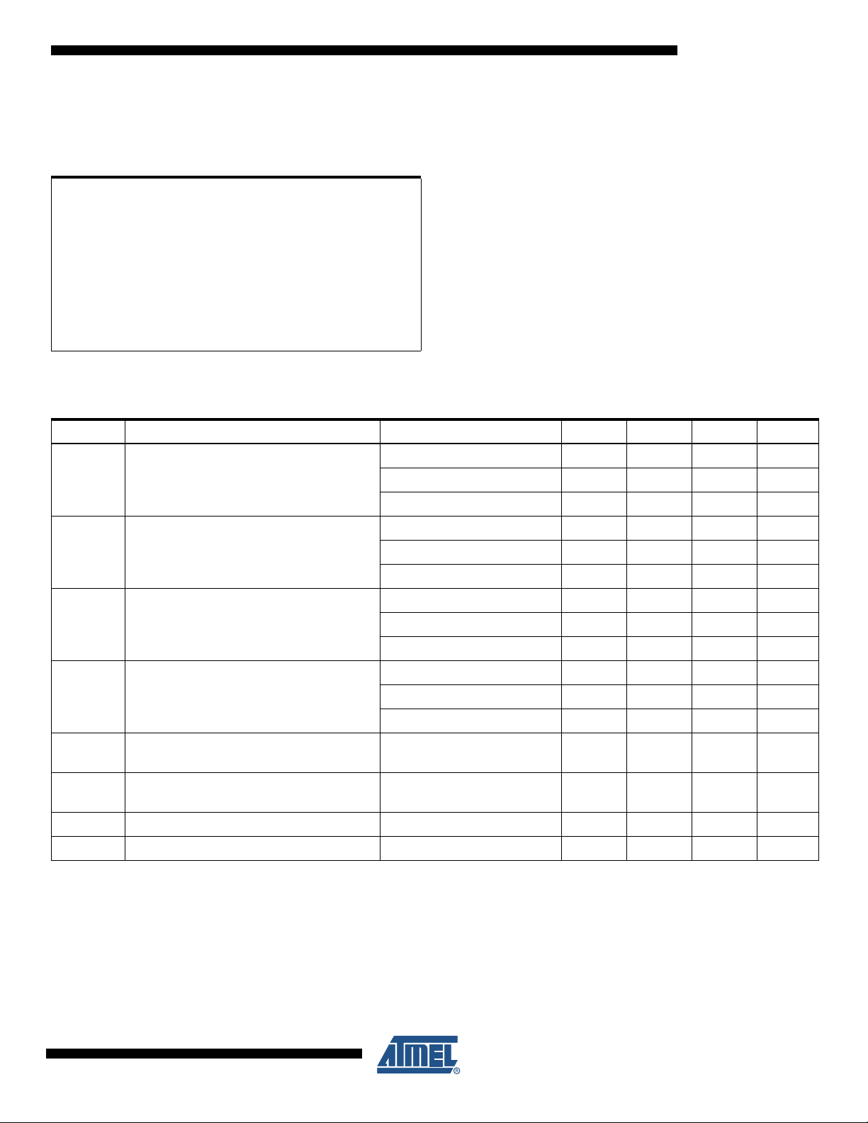
33. Electrical Characteristics - TBD
33.1 Absolute Maximum Ratings*
XMEGA A1
Operating Temperature.................................. -55°C to +125°C
*NOTICE: Stresses beyond those listed under “Absolute
Maximum Ratings” may cause permanent dam-
Storage Temperature..................................... -65°C to +150°C
age to the device. This is a stress rating only and
functional operation of the device at these or
Voltage on any Pin with respect to Ground..-0.5V to V
CC
+0.5V
other conditions beyond those indicated in the
operational sections of this specification is not
Maximum Operating Voltage ............................................3.6V
implied. Exposure to absolute maximum rating
conditions for extended periods may affect
DC Current per I/O Pin............................................... 20.0 mA
DC Current
V
and GND Pins................................200.0 mA
CC
device reliability.
33.2 DC Characteristics
TA = -40°C to 85°C, VCC = 1.6V to 3.6V (unless otherwise noted)
Symbol Parameter Condition Min. Typ. Max. Units
V
= 3.3V -0.5 0.3V
V
V
I
I
I
I
R
R
OL
OH
IL
IH
IL
IH
RST
PU
CC
Input Low Voltage
Input High Voltage
Output Sink Current
Output Source Current
Input Leakage
Current I/O Pin
Input Leakage
Current I/O Pin
= 2.7V, -0.5 0.3V
V
CC
= 1.8V, -0.5 0.3V
V
CC
V
= 3.3V, 0.7V
CC
= 2.7V, 0.7V
V
CC
= 1.8V, 0.7V
V
CC
V
= 3.3V, VOL = 0.2V
CC
= 2.7V, VOL = 0.2V
V
CC
= 1.8V, VOL = 0.2V
V
CC
V
= 3.3V, VOH = 0.8V
CC
= 2.7V, VOH = 0.8V
V
CC
= 1.8V, VOH = 0.8V
V
CC
CC
CC
CC
CC
CC
CC
CC
CC
CC
20 mA
17 mA
10 mA
10 mA
7mA
3mA
<0.001 µA
<0.001 µA
Reset Pull-up Resistor 20 kΩ
I/O Pin Pull-up Resistor 20 kΩ
CC
CC
CC
VCC+0.5 V
VCC+0.5 V
VCC+0.5 V
V
V
V
8067C–AVR–05/08
62
Page 63
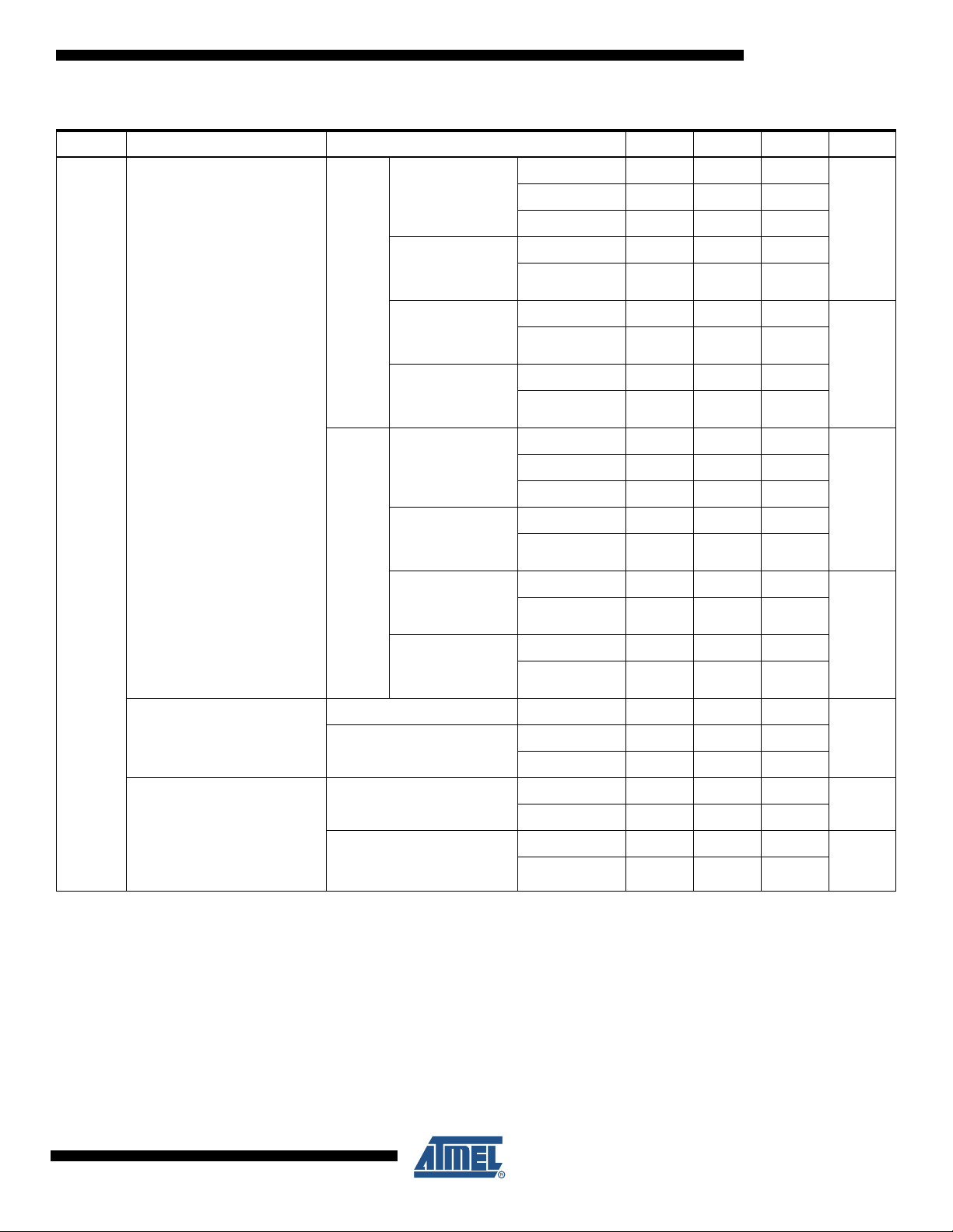
XMEGA A1
TA = -40°C to 85°C, VCC = 1.6V to 3.6V (unless otherwise noted)
Symbol Parameter Condition Min. Typ. Max. Units
= 1.8V 350
V
1 MHz,
Ext. Clock
All PRR set
2 MHz
= 1.8V
V
CC
Active
All PRR Set
32 MHz,
V
= 2.7V
CC
All PRR Set
32 MHz,
= 3.3V
V
CC
All PRR Set
Power Supply Current
1 MHz,
Ext. Clock
All PRR set
I
CC
Idle
2 MHz
= 1.8V
V
CC
All PRR Set
32 MHz,
V
= 2.7V
CC
All PRR Set
32 MHz,
= 3.3V
V
CC
All PRR Set
All Functions Disabled V
Power-down mode
ULP, WDT, Sampled BOD
Enabled
ULP, RTC,WDT, BOD
Enabled,
Power -save mode
RTC Enabled,
1 kHz from Low Power
TOSC32
Note: 1. “Max” means the highest value where the pin is guaranteed to be read as low
2. “Min” means the lowest value where the pin is guaranteed to be read as high
CC
= 2.7V 650
V
CC
V
= 3.3V 880
CC
Internal RC 720
Ext. Clock 670
Internal RC TBD
Ext. Clock 16
Internal RC TBD
Ext. Clock 21
= 1.8V 130
V
CC
= 2.7V 220
V
CC
= 3.3V 290
V
CC
Internal RC 310
Ext. Clock 260
Internal RC TBD
Ext. Clock 7
Internal RC TBD
Ext. Clock 9.2
= 1.8V 0.1
CC
V
= 1.8V 1.1
CC
= 3.3V 1.5
V
CC
V
= 1.8V 1.1
CC
= 3.3V 1.5
V
CC
= 1.8V 650
V
CC
= 3.3V 650
V
CC
µA
mA
µA
mA
µA
µA
nA
8067C–AVR–05/08
63
Page 64

33.3 Speed
XMEGA A1
The maximum frequency of the XMEGA A1 devices is depending on VCC. As shown in Figure
33-1 on page 64 the Frequency vs. V
Figure 33-1. Maximum Frequency vs. Vcc
MHz
32
curve is linear between 1.8V < VCC < 2.7V.
CC
12
1.6
1.8
Safe Operating Area
2.7
3.6
V
8067C–AVR–05/08
64
Page 65
XMEGA A1
33.4 ADC Characteristics – TBD
Table 33-1. ADC Characteristics
Symbol Parameter Condition Min Typ Max Units
Resolution 8 12 12 LSB
Integral Non-Linearity (INL) TBD LSB
Differential Non-Linearity (DNL) TBD LSB
Gain Error TBD LSB
Offset Error TBD LSB
Conversion Time
ADC Clock Frequency 100 2000 kHz
AVCC DC Supply Voltage 1.6 3.6 V
Source Impedance 2 Msps sample rate 3 kΩ
Start-up time TBD µs
AVCC Analog Supply Voltage VCC - 0.3 VCC + 0.3 V
8-bit Result 2.5 µs
12-bit Result 3.5 µs
Table 33-2. ADC Gain Stage Characteristics
Symbol Parameter Condition Min Typ Max Units
Input Capacitance TBD pF
AREF = Int. 1.0V -5
AREF = Ext. 2.5V -3
AREF = Int. 1.0V -5
AREF = Ext. 2.5V -3
AREF = Int. 1.0V -5
AREF = Ext. 2.5V -2.5
AREF = Int. 1.0V -5
AREF = Ext. 2.5V -2
AREF = Int. 1.0V -4
AREF = Ext. 2.5V -1.5
AREF = Int. 1.0V -3
AREF = Ext. 2.5V 0
AREF = Int. 1.0V 3
AREF = Ext. 2.5V 5
Offset Error
1X Gain,
VCC = 3.3V
2X Gain,
VCC = 3.3V
4X Gain,
VCC = 3.3V
8X Gain,
VCC = 3.3V
16X Gain,
VCC = 3.3V
32X Gain,
VCC = 3.3V
64X Gain,
VCC = 3.3V
LSB
8067C–AVR–05/08
65
Page 66

XMEGA A1
Table 33-2. ADC Gain Stage Characteristics (Continued)
Symbol Parameter Condition Min Typ Max Units
1X Gain,
VCC = 3.3V
AREF = Int. 1.0V TBD
AREF = Ext. 2.5V TBD
Gain Error
Signal-to-Noise Ratio (SNR)
2X Gain,
VCC = 3.3V
4X Gain,
VCC = 3.3V
8X Gain,
VCC = 3.3V
16X Gain,
VCC = 3.3V
32X Gain,
VCC = 3.3V
64X Gain,
VCC = 3.3V
1X Gain,
VCC = 3.3V
2X Gain,
VCC = 3.3V
4X Gain,
VCC = 3.3V
8X Gain,
VCC = 3.3V
16X Gain,
VCC = 3.3V
32X Gain,
VCC = 3.3V
64X Gain,
VCC = 3.3V
AREF = Int. 1.0V TBD
AREF = Ext. 2.5V TBD
AREF = Int. 1.0V TBD
AREF = Ext. 2.5V TBD
AREF = Int. 1.0V TBD
AREF = Ext. 2.5V TBD
AREF = Int. 1.0V TBD
AREF = Ext. 2.5V TBD
AREF = Int. 1.0V TBD
AREF = Ext. 2.5V TBD
AREF = Int. 1.0V TBD
AREF = Ext. 2.5V TBD
AREF = Int. 1.0V 76.3
AREF = Ext. 1.7V 75.7
AREF = Ext. 2.5V 74.6
AREF = Int. 1.0V 71.2
AREF = Ext. 1.7V 72.2
AREF = Ext. 2.5V 71.6
AREF = Int. 1.0V 64.8
AREF = Ext. 1.7V 66.8
AREF = Ext. 2.5V 67.7
AREF = Int. 1.0V 57.1
AREF = Ext. 1.7V 59.3
AREF = Ext. 2.5V 60.8
AREF = Int. 1.0V 48.2
AREF = Ext. 1.7V 50.5
AREF = Ext. 2.5V 52.2
AREF = Int. 1.0V 39.3
AREF = Ext. 1.7V 41.6
AREF = Ext. 2.5V 43.2
AREF = Int. 1.0V 30.2
AREF = Ext. 1.7V 32.4
AREF = Ext. 2.5V 34.3
LSB
dB
8067C–AVR–05/08
66
Page 67

XMEGA A1
Table 33-2. ADC Gain Stage Characteristics (Continued)
Symbol Parameter Condition Min Typ Max Units
Signal Range TBD V
DC Supply Current TBD mA
Start-up time TBD
33.5 DAC Characteristics – TBD
Table 33-3. DAC Characteristics
Symbol Parameter Condition Min Typ Max Units
Resolution 12 12 LSB
Integral Non-Linearity (INL) TBD LSB
Differential Non-Linearity (DNL) TBD LSB
Gain Error TBD LSB
Offset Error TBD LSB
Calibrated Gain/Offset Error TBD LSB
Output Range TBD V
Output Settling Time TBD µs
Output Capacitance TBD nF
Output Resistance TBD kΩ
Reference Input Voltage TBD V
# clk
cycles
Reference Input Capacitance TBD pF
Reference Input Resistance TBD kΩ
Current Consumption TBD mA
Start-up time TBD µs
33.6 Analog Comparator Characteristics – TBD
Table 33-4. Analog Comparator Characteristics
Symbol Parameter Condition Min Typ Max Units
Offset 0.5 mV
No, High Speed mode 0
No, Low Power mode 0 mV
Small, High Speed mode 3 mV
Hysteresis
Small, Low Power mode 3 mV
Large, High Speed mode 25 mV
Large, Low Power mode 30 mV
High Speed mode 50
Propagation Delay
Low power mode 130
ns
8067C–AVR–05/08
67
Page 68

XMEGA A1
Table 33-4. Analog Comparator Characteristics
Symbol Parameter Condition Min Typ Max Units
High Speed mode TBD
Current Consumption
Low power mode TBD
Start-up time TBD µs
µA
8067C–AVR–05/08
68
Page 69

34. Typical Characteristics - TBD
XMEGA A1
8067C–AVR–05/08
69
Page 70

35. Errata
35.1 ATxmega128A1 rev. G
1. Bootloader Section in Flash is non-functional
The Bootloader Section is non-functional, and bootloader or application code cannot reside
in this part of the Flash.
Problem fix/Workaround
None, do not use the Bootloader Section.
2. Bandgap voltage input for the ACs cannot be changed when used for both ACs
simultaneously
If the Bandgap voltage is selected as input for one Analog Comparator (AC) and then
selected/deselected as input for the another AC, the first comparator will be affected for up
to 1 us and could potentially give a wrong comparison result.
Problem fix/Workaround
If the Bandgap is required for both ACs simultaneously, configure the inp ut selection for both
ACs before enabling any of them.
XMEGA A1
3. DAC is nonlinear and inaccurate when reference is above 2.4V
Using the DAC with a reference voltage above 2.4V give inaccurate output when converting
codes that give below 0.75V output:
– ±20 LSB for continuous mode
– ±200 LSB for Sample and Hold mode
Problem fix/Workaround
None, avoid using a voltage reference above 2.4V.
4. ADC gain stage output range is limited to 2.6 V.
The amplified output of the ADC gain stage will never go above 2.6V, hence the differential
input will only give correct output when below 2.6V/gain. For the available gain settings, this
gives a differential input range of:
– 1X gain: 2.6V
– 2X gain: 1.3V
– 4X gain: 0.65V
– 8X gain: 325 mV
– 16X gain: 163 mV
– 32X gain: 82 mV
– 64X gain: 41 mV
Problem fix/Workaround
Keep the amplified voltage output from the ADC gain stage below 2.6V in order to get a correct result, or keep ADC voltage reference is below2.6V.
8067C–AVR–05/08
70
Page 71

XMEGA A1
5. The ADC has up to ±2 LSB inaccuracy
The ADC will have up to ±2 LSB inaccuracy, visible as a saw-tooth pattern on the input voltage/ output value transfer function of the ADC. The inaccuracy increases with increasing
voltage reference reaching ±2 LSB with 3V reference.
Problem fix/Workaround
None, the actual ADC resolution will be reduced with up to ±2 LSB.
6. TWI, a general address call will match independent of the R/W-bit value.
When the TWI is in Slave mode and a general add ress call is issued on the bus, the TWI
Slave will get an address match regardless of the R/W-bit (ADDR[0] bit) value in the Slave
Address Register.
Problem fix/Workaround
Use software to check the R/W-bit on general call address match .
7. TWI, the minimum I
2
C SCL low time could be violated in Master Read mode
When the TWI is in Master Read mode and issuing a Repeated Start on the bus, this will
immediately release the SCL line even if one complete SCL low period has not passed. This
means that the minimum SCL low time in the I
2
C specification could be violated.
Problem fix/Workaround
If this causes a potential problem in the application , soft ware must ensure that t he Repeat ed
Start is never issued before one SCL low time has passed.
8. Setting HIRES PR bit makes PWM output unavailable
Setting the HIRES Power Reduction (PR) bit for PORTx will make any Frequency or PWM
output for the corresponding Timer/Counter s (TCx0 and TCx1) unavailable on the pin.
Problem fix/Workaround
Do not write the HIRES PR bit on PORTx when frequency or PWM output from TCx0/1 is
used.
9. EEPROM erase and write does not work with all System Clock sources
When doing EEPROM erase or Write operations with other clock sources than the 2 MHz
RCOSC, Flash will be read wrongly for one or two clock cycles at the end of the EEPROM
operation.
Problem fix/Workaround
Alt 1: Use the internal 2 MHz RCOSC when doing erase or write operations on EEPROM.
8067C–AVR–05/08
Alt 2: Ensure to be in sleep mode while completing erase or write on EEPROM. Af ter starting
erase or write operations on EEPROM, other interrupts should be disabled and the device
put to sleep.
71
Page 72

36. Datasheet Revision History
36.1 8067C – 05/08
1. Updated the Front page and “Features” on page 1.
2. Updated the “DC Characteristics” on page 62.
3. Updated Figure 3-1 on page 5.
4. Added “Flash and EEPROM Page Size” on page 14.
5. Updated Table 33-2 on page 65 with new data: Gain Error, Offset Error and Signal -to-Noise
Ratio (SNR).
6. Updated Errata “ATxmega128A1 rev. G” on page 70.
36.2 8067B – 05/08
XMEGA A1
1. Updated “Pinout/Block Diagram” on page 2 and “Pinout and Pin Functions” on page 48.
2. Added XMEGA A1 Block Diagram, Figure 3-1 on page 5.
3. Updated “Overview” on page 4 included the XMEGA A1 explanation text on page 6.
4. Updated AVR CPU “Features” on page 7.
5. Updated Event System block diagram, Figure 9-1 on page 17.
6. Updated “PMIC - Programmable Multi-level Interrupt Controller” on page 24.
7. Updated “AC - Analog Comparator” on page 43.
8. Updated “Alternate Pin Function Description” on page 48.
9. Updated “Alternate Pin Functions” on page 50.
10. Updated “Typical Characteristics - TBD” on page 69.
11. Updated “Ordering Information” on page 2.
12. Updated “Overview” on page 4.
13. Updated Figure 6-1 on page 7.
14. Inserted a new Figure 15-1 on page 31.
15. Updated Speed grades in “Speed” on page 64.
16. Added a new ATxmega384A1 device in “Features” on page 1, updated “Ordering Information” on
page 2 and “Memories” on page 9.
17. Replaced the Figure 3-1 on page 5 by a new XMEGA A1 detailed block diagram.
18. Inserted Errata “ATxmega128A1 rev. G” on page 70.
8067C–AVR–05/08
72
Page 73

36.3 8067A – 02/08
XMEGA A1
1. Initial revision.
8067C–AVR–05/08
73
Page 74

Table of Contents
Features.....................................................................................................1
Typical Applications ................................................................................1
1 Ordering Information ...............................................................................2
2 Pinout/Block Diagram ..............................................................................2
3 Overview ...................................................................................................4
3.1 Block Diagram ....... ... ... ... .... ... .......................................... ... ...............................5
4 Resources .................................................................................................6
4.1 Recommended re ad in g .. .... ...............................................................................6
5 Disclaimer .................................................................................................6
6 AVR CPU ...................................................................................................7
6.1 Features ............................................................................................................7
XMEGA A1
6.2 Overview ......... ....................... ...................... ....................... ....................... ........ 7
6.3 Register File ......................................................................................................8
6.4 ALU - Arithmetic Logic Unit ...............................................................................8
6.5 Program Flow ....................................................................................................8
7 Memories ..................................................................................................9
7.1 Features ............................................................................................................9
7.2 Overview ......... ....................... ...................... ....................... ....................... ........ 9
7.3 In-System Programmable Flash Program Memory ...........................................9
7.4 Data Memory ...................................................................................................10
7.5 Signature Rows ...............................................................................................13
7.6 Flash and EEPROM Page Size .......................................................................14
8 DMAC - Direct Memory Access Controller ..........................................15
8.1 Features ..........................................................................................................15
8.2 Overview ......... ....................... ...................... ....................... ....................... ...... 15
9 Event System ..........................................................................................16
9.1 Features ..........................................................................................................16
9.2 Overview ......... ....................... ...................... ....................... ....................... ...... 16
10 System Clock and Clock options .........................................................18
10.1 Features ..........................................................................................................18
10.2 Overview ...................... ....................... ...................... ....................... ................18
8067C–AVR–05/08
i
Page 75

10.3 Clock Options .................................................................. ................................19
11 Power Management and Sleep Modes .................................................21
11.1 Features ..........................................................................................................21
11.2 Overview ...................... ....................... ...................... ....................... ................21
11.3 Sleep Modes ....................................................................................................21
12 System Control and Reset ....................................................................22
12.1 Features ..........................................................................................................22
12.2 Resetting the AVR ...........................................................................................22
12.3 Reset Sources .................................................................................................22
12.4 WDT - Watchdog Timer ...... ... ... .......................................... ... ..........................23
13 PMIC - Programmable Multi-level Interrupt Controller ....................... 24
13.1 Features ..........................................................................................................24
13.2 Overview ...................... ....................... ...................... ....................... ................24
XMEGA A1
13.3 Interrupt vectors .................................. ... ... ... .... ... .............................................24
14 I/O Ports ..................................................................................................26
14.1 Features ..........................................................................................................26
14.2 Overview ...................... ....................... ...................... ....................... ................26
14.3 I/O configuration ..............................................................................................26
14.4 Input sensing ...................... ... ... ... .... .......................................... ......................29
14.5 Port Interrupt ... ... .... ... .......................................................................................2 9
14.6 Alternate Port Functions ..................................................................................29
15 T/C - 16-bit Timer/Counter .....................................................................30
15.1 Features ..........................................................................................................30
15.2 Overview ...................... ....................... ...................... ....................... ................30
16 AWEX - Advanced Waveform Extension .............................................32
16.1 Features ..........................................................................................................32
16.2 Overview ...................... ....................... ...................... ....................... ................32
17 Hi-Res - High Resolution Extension .....................................................33
17.1 Features ..........................................................................................................33
17.2 Overview ...................... ....................... ...................... ....................... ................33
18 RTC - 16-bit Real-Time Counter ............................................................ 34
18.1 Features ..........................................................................................................34
18.2 Overview ...................... ....................... ...................... ....................... ................34
8067C–AVR–05/08
ii
Page 76

19 TWI - Two-Wire Interface .......................................................................35
19.1 Features ..........................................................................................................35
19.2 Overview ...................... ....................... ...................... ....................... ................35
20 SPI - Serial Peripheral Interface ............................................................36
20.1 Features ..........................................................................................................36
20.2 Overview ...................... ....................... ...................... ....................... ................36
21 USART ..................................................................................................... 37
21.1 Features ..........................................................................................................37
21.2 Overview ...................... ....................... ...................... ....................... ................37
22 IRCOM - IR Communication Module .....................................................38
22.1 Features ..........................................................................................................38
22.2 Overview ...................... ....................... ...................... ....................... ................38
23 Crypto Engine .........................................................................................39
XMEGA A1
23.1 Features ..........................................................................................................39
23.2 Overview ...................... ....................... ...................... ....................... ................39
24 ADC - 12-bit Analog to Digital Converter .............................................40
24.1 Features ..........................................................................................................40
24.2 Overview ...................... ....................... ...................... ....................... ................40
25 DAC - 12-bit Digital to Analog Converter .............................................42
25.1 Features ..........................................................................................................42
25.2 Overview ...................... ....................... ...................... ....................... ................42
26 AC - Analog Comparator .......................................................................43
26.1 Features ..........................................................................................................43
26.2 Overview ...................... ....................... ...................... ....................... ................43
26.3 Input Selection .......... ... ... .... ... ... ... .......................................... .... ......................45
26.4 Window Function ................................................ ... ... .... ... ................................45
27 OCD - On-chip Debug ............................................................................46
27.1 Features ..........................................................................................................46
27.2 Overview ...................... ....................... ...................... ....................... ................46
28 Program and Debug Interfaces .............................................................47
28.1 Features ..........................................................................................................47
28.2 Overview ...................... ....................... ...................... ....................... ................47
28.3 JTAG interface .................................................................................................47
8067C–AVR–05/08
iii
Page 77

28.4 PDI - Program and Debug Interface ................................................................47
29 Pinout and Pin Functions ......................................................................48
29.1 Alternate Pin Function Description ..................................................................48
29.2 Alternate Pin Functions ...................................................................................50
30 Peripheral Module Address Map .......................................................... 54
31 Instruction Set Summary .......................................................................56
32 Packaging information .......................................................................... 60
32.1 100A ................................................................................................................60
32.2 100C1 ..............................................................................................................61
33 Electrical Characteristics - TBD ............................................................62
33.1 Absolute Maximum Ratings* ...........................................................................62
33.2 DC Characteristics . ... .......................................... ... ..........................................62
33.3 Speed ..............................................................................................................64
XMEGA A1
33.4 ADC Characteristics – TBD ............................................. ... ... .... ......................65
33.5 DAC Characteristics – TBD ............................................. ... ... .... ......................67
33.6 Analog Comparator Characteristics – TBD .....................................................67
34 Typical Characteristics - TBD ...............................................................69
35 Errata ....................................................................................................... 70
35.1 ATxmega128A1 rev. G ................................................. ... ... .............................70
36 Datasheet Revision History ...................................................................72
36.1 8067C – 05/08 .................................................................................................72
36.2 8067B – 05/08 .................................................................................................72
36.3 8067A – 02/08 .................................................................................................73
Table of Contents.......................................................................................i
8067C–AVR–05/08
iv
Page 78

Headquarters International
Atmel Corporation
2325 Orchard Parkway
San Jose, CA 95131
USA
Tel: 1(408) 441-0311
Fax: 1(408) 487-2600
Atmel Asia
Room 1219
Chinachem Golden Plaza
77 Mody Road Tsimshatsui
East Kowloon
Hong Kong
Tel: (852) 2721-9778
Fax: (852) 2722-1369
Product Contact
Web Site
www.atmel.com
Literature Requests
www.atmel.com/literature
Atmel Europe
Le Krebs
8, Rue Jean-Pierre Timbaud
BP 309
78054 Saint-Quentin-enYvelines Cedex
France
Tel: (33) 1-30-60-70-00
Fax: (33) 1-30-60-71-11
Technical Support
avr@atmel.com
Atmel Japan
9F, Tonetsu Shinkawa Bldg.
1-24-8 Shinkawa
Chuo-ku, Tokyo 104-0033
Japan
Tel: (81) 3-3523-3551
Fax: (81) 3-3523-7581
Sales Contact
www.atmel.com/contacts
Disclaimer: The information in this document is provided in connection with Atmel products. No license, express or implied, by estoppel or otherwise, to any
intellectual property r ight is granted by this document or in connection with the sale of Atmel products. EXCEPT AS SET FORTH IN ATMEL’S TERMS AND CONDI-
TIONS OF SALE LOCATED ON ATMEL’S WEB SITE, ATMEL ASSUMES NO LIABILITY WHATSOEVER AND DISCLAIMS ANY EXPRESS, IMPLIED OR STATUTORY
WARRANTY RELATING TO ITS PRODUCTS INCLUDING, BUT NOT LIMITED TO, THE IMPLIED WARRANTY OF MERCHANTABILITY, FITNESS FOR A PARTICULAR
PURPOSE, OR NON-INFRINGEMENT. IN NO EVENT SHALL ATMEL BE LIABLE FOR ANY DIRECT, INDIRECT, CONSEQUENTIAL, PUNITIVE, SPECIAL OR INCIDENT AL DAMAGES (INCLUDING, WITHOUT LIMITATION, DAMAGES FOR LOSS OF PROFITS, BU SINESS I NTERR UPTI ON, OR L OSS OF INFORMATION) ARISING OUT OF
THE USE OR INABILITY TO USE THIS DOCUMENT, EVEN IF ATMEL HAS BEEN ADVISED OF THE POSSIBILITY OF SUCH DAMAGES. Atmel makes no
representations or warranties with respect to the accuracy or completeness of the contents of this document and reserves the right to make changes to specifications
and product descriptions at any time without notice. Atmel does not make any commitment to update the information contained here in. Unless specifically provided
otherwise, Atmel products are not suitable for, and shall not be used in, automotive applications. Atmel’s products are not intended, authorized, or warranted for use
as components in applications intended to suppor t or sustain life.
© 2008 Atmel Corporation. All rights reserved. Atmel®, logo and combinations thereof, AVR® and others are registered trademarks, XMEGA
TM
and others aretrademarks of Atmel Corporation or its subsidiaries. Other terms an d product names may be trademarks of others.
8067C–AVR–05/08
 Loading...