

Features
• High-performance, Low-power 8/16-bit AVR XMEGA Microcontroller
• Non-volatile Program and Data Memories
– 16 KB - 128 KB of In-System Self-Programmable Flash
– 4 KB - 8 KB Boot Code Section with Independent Lock Bits
– 1 KB - 2 KB EEPROM
– 2 KB - 8 KB Internal SRAM
• Peripheral Features
– Four-channel DMA Controller with support for external requests
– Eight-channel Event System
– Five 16-bit Timer/Counters
Three Timer/Counters with 4 Output Compare or Input Capture channels
Two Timer/Counters with 2 Output Compare or Input Capture channels
High-Resolution Extensions on all Timer/Counters
Advanced Waveform Extension on one Timer/Counter
– Five USARTs
IrDA Extension on one USART
– Two Two-Wire Interfaces with dual address match (I
– Two SPIs (Serial Peripheral Interfaces) peripherals
– AES and DES Crypto Engine
– 16-bit Real Time Counter with Separate Oscillator
– One Twelve-channel, 12-bit, 2 Msps Analog to Digital Converter
– One Two-channel, 12-bit, 1 Msps Digital to Analog Converter
– Two Analog Comparators with Window compare function
– External Interrupts on all General Purpose I/O pins
– Programmable Watchdog Timer with Separate On-chip Ultra Low Power Oscillator
• Special Microcontroller Features
– Power-on Reset and Programmable Brown-out Detection
– Internal and External Clock Options with PLL
– Programmable Multi-level Interrupt Controller
– Sleep Modes: Idle, Power-down, Standby, Power-save, Extended Standby
– Advanced Programming, Test and Debugging Interfaces
PDI (Program and Debug Interface) for programming, test and debugging
• I/O and Packages
– 34 Programmable I/O Lines
– 44 - lead TQFP
– 44 - pad VQFN/QFN
– 49 - ball VFBGA
• Operating Voltage
– 1.6 – 3.6V
• Speed performance
– 0 – 12 MHz @ 1.6 – 3.6V
– 0 – 32 MHz @ 2.7 – 3.6V
2
C and SMBus compatible)
8/16-bit
XMEGA A4
Microcontroller
ATxmega128A4
ATxmega64A4
ATxmega32A4
ATxmega16A4
Preliminary
Typical Applications
• Industrial control • Climate control • Hand-held battery applications
• Factory automation • ZigBee • Power tools
• Building control • Motor control • HVAC
• Board control • Networking • Metering
• White Goods • Optical • Medical Applications
8069L–AVR–11/09
1. Ordering Information
XMEGA A4
Ordering Code Flash E
ATxmega128A4-AU 128 KB + 8 KB 2 KB 8 KB 32 1.6 - 3.6V
ATxmega64A4-AU 64 KB + 4 KB 2 KB 4 KB 32 1.6 - 3.6V
ATxmega32A4-AU 32 KB + 4 KB 1 KB 4 KB 32 1.6 - 3.6V
ATxmega16A4-AU 16 KB + 4 KB 1 KB 2 KB 32 1.6 - 3.6V
ATxmega128A4-MH 128 KB + 8 KB 2 KB 8 KB 32 1.6 - 3.6V
ATxmega64A4-MH 64 KB + 4 KB 2 KB 4 KB 32 1.6 - 3.6V
ATxmega32A4-MH 32 KB + 4 KB 1 KB 4 KB 32 1.6 - 3.6V
ATxmega16A4-MH 16 KB + 4 KB 1 KB 2 KB 32 1.6 - 3.6V
ATxmega32A4-CU 32 KB + 4K 1 KB 4 KB 32 1.6 - 3.6V
ATxmega16A4-CU 16 KB + 4 KB 1 KB 2 KB 32 1.6 - 3.6V
2
SRAM Speed (MHz) Power Supply Package
44A
44M1
49C2
(1)(2)(3)
Tem p
-40°C - 85°C
Notes: 1. This device can also be supplied in wafer form. Please contact your local Atmel sales office for detailed ordering information.
2. Pb-free packaging, complies to the European Directive for Restriction of Hazardous Substances (RoHS directive). Also
Halide free and fully Green.
3. For packaging information see ”Packaging information” on page 58.
Package Type
44A 44-Lead, 10 x 10 mm Body Size, 1.0 mm Body Thickness, 0.8 mm Lead Pitch, Thin Profile Plastic Quad Flat Package (TQFP)
44M1 44-Pad, 7x7x1 mm Body, Lead Pitch 0.50 mm, 5.20 mm Exposed Pad, Thermally Enhanced Plastic Very Thin Quad No Lead Package (VQFN)
49C2 49-Ball (7 x 7 Array), 0.65 mm Pitch, 5.0 x 5.0 x 1.0 mm, Very Thin, Fine-Pitch Ball Grid Array Package (VFBGA)
8069L–AVR–11/09
2
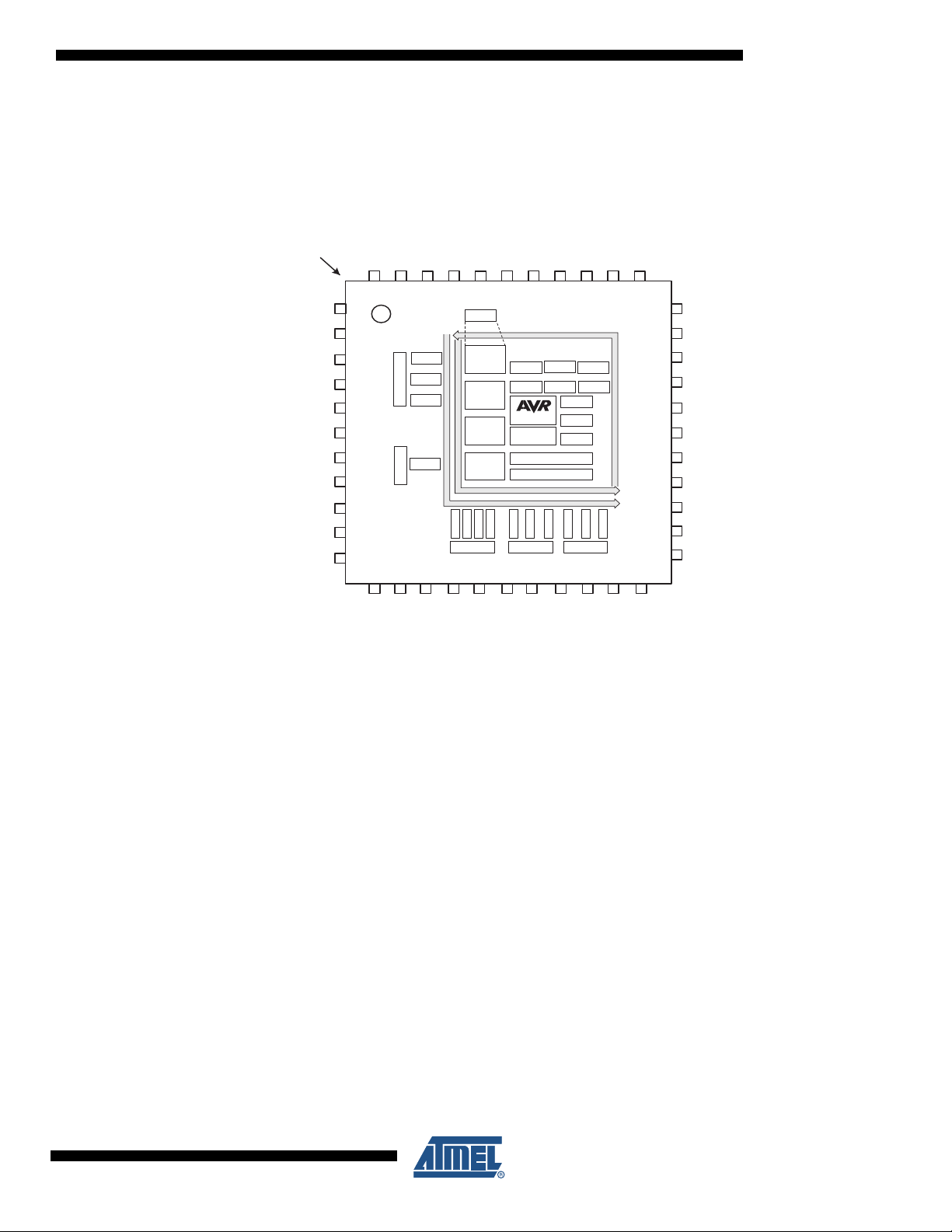
2. Pinout/Block Diagram
Figure 2-1. Bock Diagram and TQFP/QFN pinout
XMEGA A4
INDEX CORNER
PA 5
PA 6
PA 7
PB0
PB1
PB2
PB3
GND
VCC
PC0
PC1
PA 4
PA 3
PA 2
PA 1
PA 0
AVCC
GND
PR1
PR0
RESET/PDI_CLK
PDI_DATA
44
43
42
41
40
39
38
37
36
35
34
1
2
3
4
5
ADC A
A
AC A0
Port
A
AC A1
6
7
B
DAC B
Port
8
9
10
11
12
13
PC2
PC3
14
PC4
T/C0:1
Port C
15
PC5
Port R
OSC/CLK
Control
Power
Control
Reset
Control
Watchdog
USART0:1
TWI
DATA BU S
BOD POR
TEMP
CPU
DMA
Interrupt Controller
Event System ctrl
DATA BU S
EVENT ROUTING NETWORK
T/C0:1
SPI
USART0:1
Port D
16
17
PC6
PC7
VREF
RTC
OCD
FLASH
RAM
E2PROM
T/C0
SPI
USART0
Port E
18
19
20
PD0
VCC
GND
33
32
31
30
29
28
27
26
25
24
TWI
23
21
22
PD1
PD2
Note: For full details on pinout and pin functions refer to ”Pinout and Pin Functions” on page 49.
PE3
PE2
VCC
GND
PE1
PE0
PD7
PD6
PD5
PD4
PD3
8069L–AVR–11/09
3

Figure 2-2. VFBGA pinout
XMEGA A4
Top view
1 234567
A
B
C
D
E
F
G
Bottom view
7654321
A
B
C
D
E
F
G
Table 2-1. VFBGA pinout
123456
A PA3 AVCC GND PR1 PR0 PDI_DATA PE3
B
PA 4 PA1 PA 0 G ND
C PA5 PA2 PA6 PA7 GND PE1 GND
D PB1 PB2 PB3 PB0 GND PD7 PE0
E GND GND PC3 GND PD4 PD5 PD6
RESET/
PDI_CLK
PE2 VCC
F VCC PC0 PC4 PC6 PD0 PD1 PD3
G PC1 PC2 PC5 PC7 GND VCC PD2
8069L–AVR–11/09
4

3. Overview
XMEGA A4
The XMEGA™A4 is a family of low power, high performance and peripheral rich CMOS 8/16-bit
microcontrollers based on the AVR
instructions in a single clock cycle, the XMEGA A4 achieves throughputs approaching 1 Million
Instructions Per Second (MIPS) per MHz allowing the system designer to optimize power consumption versus processing speed.
The AVR CPU combines a rich instruction set with 32 general purpose working registers. All the
32 registers are directly connected to the Arithmetic Logic Unit (ALU), allowing two independent
registers to be accessed in one single instruction, executed in one clock cycle. The resulting
architecture is more code efficient while achieving throughputs many times faster than conventional single-accumulator or CISC based microcontrollers.
The XMEGA A4 devices provide the following features: In-System Programmable Flash with
Read-While-Write capabilities, Internal EEPROM and SRAM, four-channel DMA Controller,
eight-channel Event System, Programmable Multi-level Interrupt Controller, 34 general purpose
I/O lines, 16-bit Real Time Counter (RTC), five flexible 16-bit Timer/Counters with compare
modes and PWM, five USARTs, two Two Wire Serial Interfaces (TWIs), two Serial Peripheral
Interfaces (SPIs), AES and DES crypto engine, one Twelve-channel, 12-bit ADC with optional
differential input with programmable gain, one Two-channel 12-bit DAC, two analog comparators
with window mode, programmable Watchdog Timer with separate Internal Oscillator, accurate
internal oscillators with PLL and prescaler and programmable Brown-Out Detection.
The Program and Debug Interface (PDI), a fast 2-pin interface for programming and debugging,
is available.
®
enhanced RISC architecture. By executing powerful
The XMEGA A4 devices have five software selectable power saving modes. The Idle mode
stops the CPU while allowing the SRAM, DMA Controller, Event System, Interrupt Controller and
all peripherals to continue functioning. The Power-down mode saves the SRAM and register
contents but stops the oscillators, disabling all other functions until the next TWI or pin-change
interrupt, or Reset. In Power-save mode, the asynchronous Real Time Counter continues to run,
allowing the application to maintain a timer base while the rest of the device is sleeping. In
Standby mode, the Crystal/Resonator Oscillator is kept running while the rest of the device is
sleeping. This allows very fast start-up from external crystal combined with low power consumption. In Extended Standby mode, both the main Oscillator and the Asynchronous Timer continue
to run. To further reduce power consumption, the peripheral clock to each individual peripheral
can optionally be stopped in Active mode and in Idle sleep mode.
The device is manufactured using Atmel's high-density nonvolatile memory technology. The program Flash memory can be reprogrammed in-system through the PDI. A Bootloader running in
the device can use any interface to download the application program to the Flash memory. The
Bootloader software in the Boot Flash section will continue to run while the Application Flash
section is updated, providing true Read-While-Write operation. By combining an 8/16-bit RISC
CPU with In-System Self-Programmable Flash, the Atmel XMEGA A4 is a powerful microcontroller family that provides a highly flexible and cost effective solution for many embedded
applications.
The XMEGA A4 devices are supported with a full suite of program and system development
tools including: C compilers, macro assemblers, program debugger/simulators, programmers,
and evaluation kits.
8069L–AVR–11/09
5
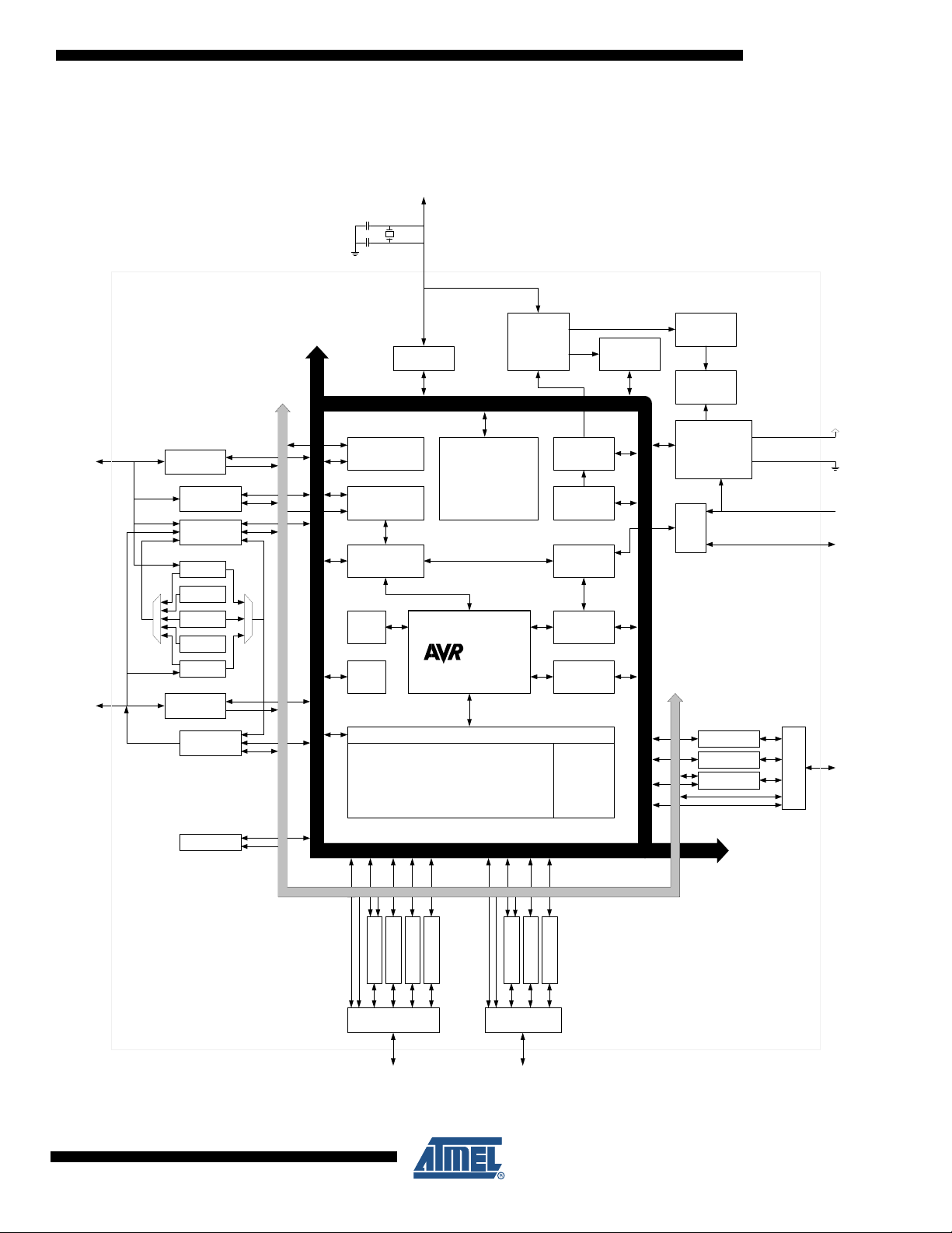
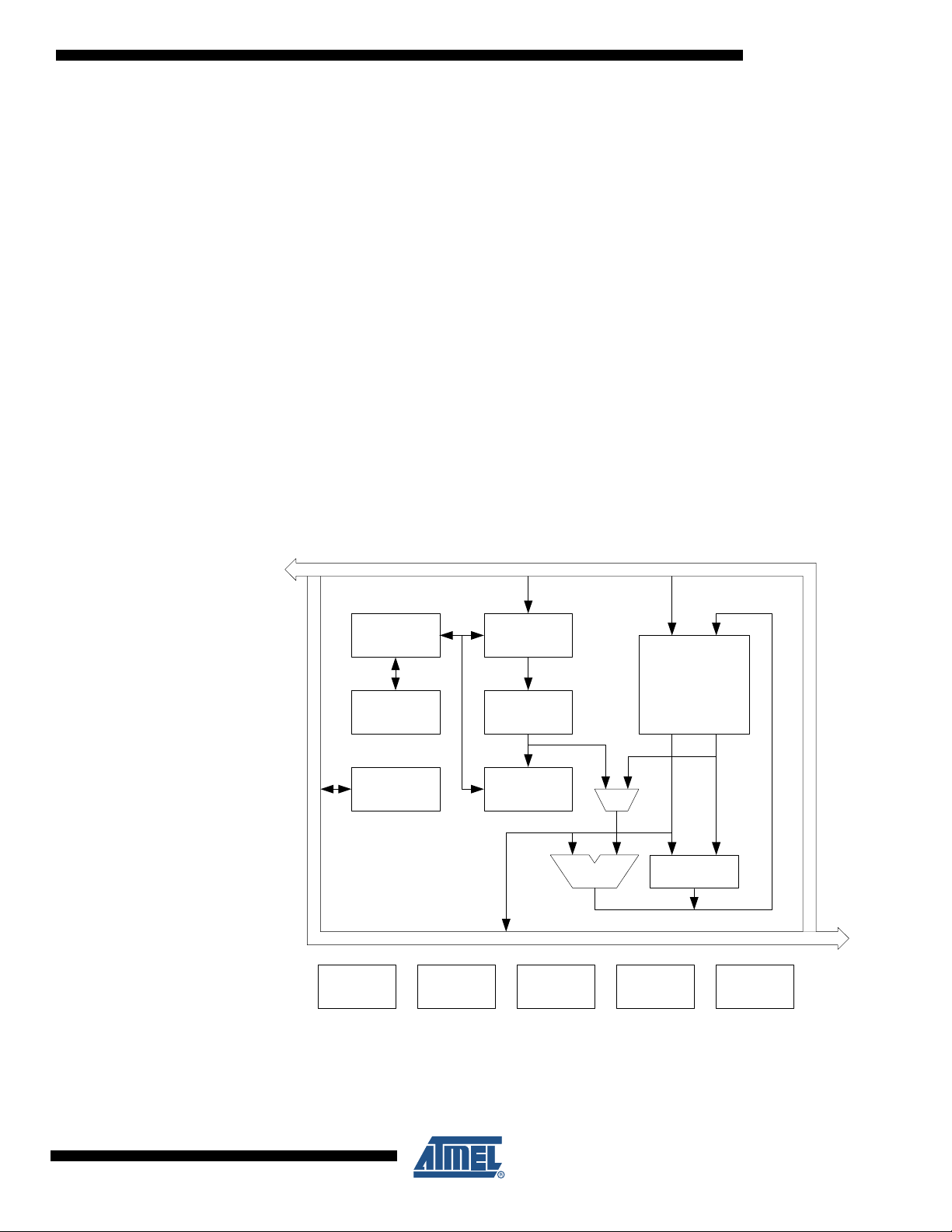
3.1 Block Diagram
PE[0..3]
PORT E (4)
TCE0
USARTE0
TWIE
Power
Supervision
POR/BOD &
RESET
PORT A (8)
PORT B (4)
DMA
Controller
BUS
Controller
SRAM
ADCA
ACA
DACB
OCD
PDI
CPU
PA[0..7]
Watchdog
Timer
Watchdog
Oscillator
Interrupt
Controller
DATA BUS
DATA BUS
Prog/Debug
Controller
VCC
GND
Oscillator
Circuits/
Clock
Generation
Oscillator
Control
Real Time
Counter
Event System
Controller
PDI_DATA
RESET/
PDI_CLK
Sleep
Controller
Flash EEPROM
NVM Controller
DES
AES
IRCOM
PORT C (8)
PC[0..7]
TCC0:1
USARTC0:1
TWIC
SPIC
PD[0..7]
PORT R (2)
XTAL1/
TOSC1
XTAL2/
TOSC2
PR[0..1]
PORT D (8)
TCD0:1
USARTD0:1
SPID
EVENT ROUTING NETWORK
PB[0..3]
Int. Ref.
AREFA
AREFB
Tempref
VCC/10
Figure 3-1. XMEGA A4 Block Diagram
XMEGA A4
8069L–AVR–11/09
6

4. Resources
A comprehensive set of development tools, application notes and datasheets are available for
download on http://www.atmel.com/avr.
4.1 Recommended reading
• XMEGA A Manual
• XMEGA A Application Notes
This device data sheet only contains part specific information and a short description of each
peripheral and module. The XMEGA A Manual describes the modules and peripherals in depth.
The XMEGA A application notes contain example code and show applied use of the modules
and peripherals.
The XMEGA A Manual and Application Notes are available from http://www.atmel.com/avr.
5. Disclaimer
For devices that are not available yet, typical values contained in this datasheet are based on
simulations and characterization of other AVR XMEGA microcontrollers manufactured on the
same process technology. Min. and Max values will be available after the device is
characterized.
XMEGA A4
8069L–AVR–11/09
7
6. AVR CPU
Flash
Program
Memory
Instruction
Decode
Program
Counter
OCD
32 x 8 General
Purpose
Registers
ALU
Multiplier/
DES
Instruction
Register
STATUS/
CONTROL
Peripheral
Module 1
Peripheral
Module 2
EEPROM PMICSRAM
DATA BUS
DATA BUS
6.1 Features
6.2 Overview
XMEGA A4
• 8/16-bit high performance AVR RISC Architecture
– 138 instructions
– Hardware multiplier
• 32x8-bit registers directly connected to the ALU
• Stack in RAM
• Stack Pointer accessible in I/O memory space
• Direct addressing of up to 16M Bytes of program and data memory
• True 16/24-bit access to 16/24-bit I/O registers
• Support for 8-, 16- and 32-bit Arithmetic
• Configuration Change Protection of system critical features
The XMEGA A4 uses the 8/16-bit AVR CPU. The main function of the CPU is program execution. The CPU must therefore be able to access memories, perform calculations and control
peripherals. Interrupt handling is described in a separate section. Figure 6-1 on page 8 shows
the CPU block diagram.
Figure 6-1. CPU block diagram
8069L–AVR–11/09
The AVR uses a Harvard architecture - with separate memories and buses for program and
data. Instructions in the program memory are executed with a single level pipeline. While one
instruction is being executed, the next instruction is pre-fetched from the program memory. This
8

concept enables instructions to be executed in every clock cycle. The program memory is InSystem Re-programmable Flash memory.
6.3 Register File
The fast-access Register File contains 32 x 8-bit general purpose working registers with single
clock cycle access time. This allows single-cycle Arithmetic Logic Unit (ALU) operation. In a typical ALU cycle, the operation is performed on two Register File operands, and the result is stored
back in the Register File.
Six of the 32 registers can be used as three 16-bit address register pointers for data space
addressing - enabling efficient address calculations. One of these address pointers can also be
used as an address pointer for look up tables in Flash program memory.
6.4 ALU - Arithmetic Logic Unit
The high performance Arithmetic Logic Unit (ALU) supports arithmetic and logic operations
between registers or between a constant and a register. Single register operations can also be
executed. Within a single clock cycle, arithmetic operations between general purpose registers
or between a register and an immediate are executed. After an arithmetic or logic operation, the
Status Register is updated to reflect information about the result of the operation.
XMEGA A4
6.5 Program Flow
The ALU operations are divided into three main categories – arithmetic, logical, and bit-functions. Both 8- and 16-bit arithmetic is supported, and the instruction set allows for efficient
implementation of 32-bit arithmetic. The ALU also provides a powerful multiplier supporting both
signed and unsigned multiplication and fractional format.
When the device is powered on, the CPU starts to execute instructions from the lowest address
in the Flash Program Memory ‘0’. The Program Counter (PC) addresses the next instruction to
be fetched. After a reset, the PC is set to location ‘0’.
Program flow is provided by conditional and unconditional jump and call instructions, capable of
addressing the whole address space directly. Most AVR instructions use a 16-bit word format,
while a limited number uses a 32-bit format.
During interrupts and subroutine calls, the return address PC is stored on the Stack. The Stack
is effectively allocated in the general data SRAM, and consequently the Stack size is only limited
by the total SRAM size and the usage of the SRAM. After reset the Stack Pointer (SP) points to
the highest address in the internal SRAM. The SP is read/write accessible in the I/O memory
space, enabling easy implementation of multiple stacks or stack areas. The data SRAM can
easily be accessed through the five different addressing modes supported in the AVR CPU.
8069L–AVR–11/09
9

7. Memories
7.1 Features
7.2 Overview
XMEGA A4
• Flash Program Memory
– One linear address space
– In-System Programmable
– Self-Programming and Bootloader support
– Application Section for application code
– Application Table Section for application code or data storage
– Boot Section for application code or bootloader code
– Separate lock bits and protection for all sections
– Built in fast CRC check of a selectable flash program memory section
• Data Memory
– One linear address space
– Single cycle access from CPU
– SRAM
– EEPROM
Byte and page accessible
Optional memory mapping for direct load and store
– I/O Memory
Configuration and Status registers for all peripherals and modules
16 bit-accessible General Purpose Register for global variables or flags
– Bus arbitration
Safe and deterministic handling of CPU and DMA Controller priority
– Separate buses for SRAM, EEPROM, I/O Memory and External Memory access
Simultaneous bus access for CPU and DMA Controller
• Production Signature Row Memory for factory programmed data
Device ID for each microcontroller device type
Serial number for each device
Oscillator calibration bytes
ADC, DAC and temperature sensor calibration data
• User Signature Row
One flash page in size
Can be read and written from software
Content is kept after chip erase
8069L–AVR–11/09
The AVR architecture has two main memory spaces, the Program Memory and the Data Memory. In addition, the XMEGA A4 features an EEPROM Memory for non-volatile data storage. All
three memory spaces are linear and require no paging. The available memory size configurations are shown in ”Ordering Information” on page 2. In addition each device has a Flash
memory signature row for calibration data, device identification, serial number etc.
Non-volatile memory spaces can be locked for further write or read/write operations. This prevents unrestricted access to the application software.
10

7.3 In-System Programmable Flash Program Memory
The XMEGA A4 devices contain On-chip In-System Programmable Flash memory for program
storage, see Figure 7-1 on page 11. Since all AVR instructions are 16- or 32-bits wide, each
Flash address location is 16 bits.
The Program Flash memory space is divided into Application and Boot sections. Both sections
have dedicated Lock Bits for setting restrictions on write or read/write operations. The Store Program Memory (SPM) instruction must reside in the Boot Section when used to write to the Flash
memory.
A third section inside the Application section is referred to as the Application Table section which
has separate Lock bits for storage of write or read/write protection. The Application Table section can be used for storing non-volatile data or application software.
Figure 7-1. Flash Program Memory (Hexadecimal address)
Word Address
XMEGA A4
0
EFFF / 77FF / 37FF / 17FF
F000 / 7800 / 3800 / 1800
FFFF / 7FFF / 3FFF / 1FFF
10000 / 8000 / 4000 / 2000
10FFF / 87FF / 47FF / 27FF
Application Section
(128 KB/64 KB/32 KB/16 KB)
...
Application Table Section
(4 KB/4 KB/4 KB/4 KB)
Boot Section
(8 KB/4 KB/4 KB/4 KB)
The Application Table Section and Boot Section can also be used for general application
software.
8069L–AVR–11/09
11
XMEGA A4
7.4 Data Memory
The Data Memory consist of the I/O Memory, EEPROM and SRAM memories, all within one linear address space, see Figure 7-2 on page 12. To simplify development, the memory map for all
devices in the family is identical and with empty, reserved memory space for smaller devices.
Figure 7-2. Data Memory Map (Hexadecimal address)
Byte Address ATxmega64A4 Byte Address ATxmega32A4 Byte Address ATxmega16A4
1000
0
I/O Registers
(4 KB)
EEPROM
(1 KB)
0
FFF FFF FFF
1000
17FF 13FF 13FF
I/O Registers
(4 KB)
EEPROM
(2 KB)
RESERVED RESERVED RESERVED
1000
0
I/O Registers
(4 KB)
EEPROM
(1 KB)
2000
2FFF 2FFF 27FF
7.4.1 I/O Memory
Internal SRAM
(4 KB)
2000
Internal SRAM
(4 KB)
2000
Internal SRAM
(2 KB)
Byte Address ATxmega128A4
0
FFF
1000
17FF
2000
3FFF
I/O Registers
(4 KB)
EEPROM
(2 KB)
RESERVED
Internal SRAM
(8 KB)
All peripherals and modules are addressable through I/O memory locations in the data memory
space. All I/O memory locations can be accessed by the Load (LD/LDS/LDD) and Store
(ST/STS/STD) instructions, transferring data between the 32 general purpose registers in the
CPU and the I/O Memory.
The IN and OUT instructions can address I/O memory locations in the range 0x00 - 0x3F
directly.
I/O registers within the address range 0x00 - 0x1F are directly bit-accessible using the SBI and
CBI instructions. The value of single bits can be checked by using the SBIS and SBIC instructions on these registers.
The I/O memory address for all peripherals and modules in XMEGA A4 is shown in the ”Periph-
eral Module Address Map” on page 53.
7.4.2 SRAM Data Memory
The XMEGA A4 devices have internal SRAM memory for data storage.
8069L–AVR–11/09
12
7.4.3 EEPROM Data Memory
The XMEGA A4 devices have internal EEPROM memory for non-volatile data storage. It is
addressable either in a separate data space or it can be memory mapped into the normal data
memory space. The EEPROM memory supports both byte and page access.
7.5 Production Signature Row
The Production Signature Row is a separate memory section for factory programmed data. It
contains calibration data for functions such as oscillators and analog modules.
The production signature row also contains a device ID that identify each microcontroller device
type, and a serial number that is unique for each manufactured device. The device ID for the
available XMEGA A4 devices is shown in Table 7-1 on page 13. The serial number consist of
the production LOT number, wafer number, and wafer coordinates for the device.
The production signature row can not be written or erased, but it can be read from both application software and external programming.
Table 7-1. Device ID bytes for XMEGA A4 devices.
ATxmega16A4 41 94 1E
XMEGA A4
Device Device ID bytes
Byte 2 Byte 1 Byte 0
7.6 User Signature Row
The User Signature Row is a separate memory section that is fully accessible (read and write)
from application software and external programming. The user signature row is one flash page
in size, and is meant for static user parameter storage, such as calibration data, custom serial
numbers or identification numbers, random number seeds etc. This section is not erased by
Chip Erase commands that erase the Flash, and requires a dedicated erase command. This
ensures parameter storage during multiple program/erase session and on-chip debug sessions.
ATxmega32A4 41 95 1E
ATxmega64A4 46 96 1E
ATxmega128A4 46 97 1E
8069L–AVR–11/09
13

XMEGA A4
7.7 Flash and EEPROM Page Size
The Flash Program Memory and EEPROM data memory are organized in pages. The pages are
word accessible for the Flash and byte accessible for the EEPROM.
Table 7-2 on page 14 shows the Flash Program Memory organization. Flash write and erase
operations are performed on one page at a time, while reading the Flash is done one byte at a
time. For Flash access the Z-pointer (Z[m:n]) is used for addressing. The most significant bits in
the address (FPAGE) give the page number and the least significant address bits (FWORD)
give the word in the page.
Table 7-2. Number of words and Pages in the Flash.
Devices Flash Page Size FWORD FPAGE Application Boot
Size (words) Size No of Pages Size No of Pages
ATxmega16A4 16 KB + 4 KB 128 Z[6:0] Z[13:7] 16 KB 64 4 KB 16
ATxmega32A4 32 KB + 4 KB 128 Z[6:0] Z[14:7] 32 KB 128 4 KB 16
ATxmega64A4 64 KB + 4 KB 128 Z[6:0] Z[15:7] 64 KB 128 4 KB 16
ATxmega128A4 128 KB + 8 KB 256 Z[7:0] Z[16:8] 128 KB 256 8 KB 16
Table 7-3 on page 14 shows EEPROM memory organization for the XMEGA A4 devices.
EEPROM write and erase operations can be performed one page or one byte at a time, while
reading the EEPROM is done one byte at a time. For EEPROM access the NVM Address Register (ADDR[m:n]) is used for addressing. The most significant bits in the address (E2PAGE) give
the page number and the least significant address bits (E2BYTE) give the byte in the page.
Table 7-3. Number of Bytes and Pages in the EEPROM.
Devices EEPROM Page Size E2BYTE E2PAGE No of Pages
Size (Bytes)
ATxmega16A4 1 KB 32 ADDR[4:0] ADDR[10:5] 32
ATxmega32A4 1 KB 32 ADDR[4:0] ADDR[10:5] 32
ATxmega64A4 2 KB 32 ADDR[4:0] ADDR[10:5] 64
ATxmega128A4 2 KB 32 ADDR[4:0] ADDR[10:5] 64
8069L–AVR–11/09
14

8. DMAC - Direct Memory Access Controller
8.1 Features
• Allows High-speed data transfer
– From memory to peripheral
– From memory to memory
– From peripheral to memory
– From peripheral to peripheral
• 4 Channels
• From 1 byte and up to 16 M bytes transfers in a single transaction
• Multiple addressing modes for source and destination address
–Increment
– Decrement
– Static
• 1, 2, 4, or 8 bytes Burst Transfers
• Programmable priority between channels
8.2 Overview
The XMEGA A4 has a Direct Memory Access (DMA) Controller to move data between memories
and peripherals in the data space. The DMA controller uses the same data bus as the CPU to
transfer data.
XMEGA A4
It has 4 channels that can be configured independently. Each DMA channel can perform data
transfers in blocks of configurable size from 1 to 64K bytes. A repeat counter can be used to
repeat each block transfer for single transactions up to 16M bytes. Each DMA channel can be
configured to access the source and destination memory address with incrementing, decrementing or static addressing. The addressing is independent for source and destination address.
When the transaction is complete the original source and destination address can automatically
be reloaded to be ready for the next transaction.
The DMAC can access all the peripherals through their I/O memory registers, and the DMA may
be used for automatic transfer of data to/from communication modules, as well as automatic
data retrieval from ADC conversions, data transfer to DAC conversions, or data transfer to or
from port pins. A wide range of transfer triggers is available from the peripherals, Event System
and software. Each DMA channel has different transfer triggers.
To allow for continuous transfer, two channels can be interlinked so that the second takes over
the transfer when the first is finished and vice versa.
The DMA controller can read from memory mapped EEPROM, but it cannot write to the
EEPROM or access the Flash.
8069L–AVR–11/09
15

9. Event System
9.1 Features
9.2 Overview
• Inter-peripheral communication and signalling with minimum latency
• CPU and DMA independent operation
• 8 Event Channels allow for up to 8 signals to be routed at the same time
• Events can be generated by
– TImer/Counters (TCxn)
– Real Time Counter (RTC)
– Analog to Digital Converters (ADCx)
– Analog Comparators (ACx)
– Ports (PORTx)
– System Clock (Clk
– Software (CPU)
SYS
)
• Events can be used by
– TImer/Counters (TCxn)
– Analog to Digital Converters (ADCx)
– Digital to Analog Converters (DACx)
– Ports (PORTx)
– DMA Controller (DMAC)
– IR Communication Module (IRCOM)
• The same event can be used by multiple peripherals for synchronized timing
• Advanced Features
– Manual Event Generation from software (CPU)
– Quadrature Decoding
– Digital Filtering
• Functions in Active and Idle mode
XMEGA A4
8069L–AVR–11/09
The Event System is a set of features for inter-peripheral communication. It enables the possibility for a change of state in one peripheral to automatically trigger actions in one or more
peripherals. Whose changes in a peripheral that will trigger actions in other peripherals are configurable by software. It is a simple, but powerful system as it allows for autonomous control of
peripherals without any use of interrupts, CPU or DMA resources.
The indication of a change in a peripheral is referred to as an event, and is usually the same as
the interrupt conditions for that peripheral. Events are passed between peripherals using a dedicated routing network called the Event Routing Network. Figure 9-1 on page 17 shows a basic
block diagram of the Event System with the Event Routing Network and the peripherals to which
it is connected. This highly flexible system can be used for simple routing of signals, pin functions or for sequencing of events.
The maximum latency is two CPU clock cycles from when an event is generated in one peripheral, until the actions are triggered in one or more other peripherals.
The Event System is functional in both Active and Idle modes.
16
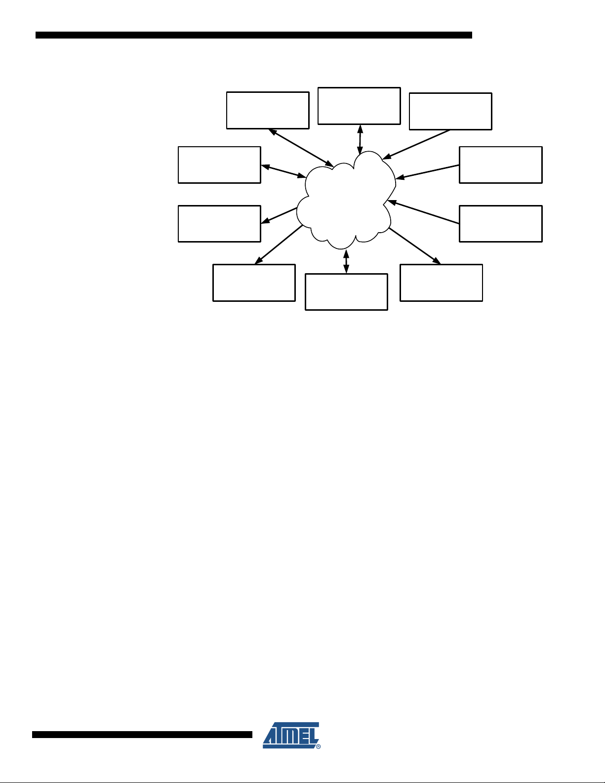
Figure 9-1. Event System Block Diagram
ADCx
DACx
Event Routing
Network
PORTx
CPU
ACx
RTC
T/Cxn
DMACIRCOM
ClkSYS
XMEGA A4
The Event Routing Network can directly connect together ADCs, DACs, Analog Comparators
(ACx), I/O ports (PORTx), the Real-time Counter (RTC), Timer/Counters (T/C) and the IR Communication Module (IRCOM). Events can also be generated from software (CPU).
All events from all peripherals are always routed into the Event Routing Network. This consist of
eight multiplexers where each can be configured in software to select which event to be routed
into that event channel. All eight event channels are connected to the peripherals that can use
events, and each of these peripherals can be configured to use events from one or more event
channels to automatically trigger a software selectable action.
8069L–AVR–11/09
17

10. System Clock and Clock options
10.1 Features
• Fast start-up time
• Safe run-time clock switching
• Internal Oscillators:
– 32 MHz run-time calibrated RC oscillator
– 2 MHz run-time calibrated RC oscillator
– 32.768 kHz calibrated RC oscillator
– 32 kHz Ultra Low Power (ULP) oscillator with 1 kHz ouput
• External clock options
– 0.4 - 16 MHz Crystal Oscillator
– 32 kHz Crystal Oscillator
– External clock
• PLL with internal and external clock options with 1 to 31x multiplication
• Clock Prescalers with 1 to 2048x division
• Fast peripheral clock running at 2 and 4 times the CPU clock speed
• Automatic Run-Time Calibration of internal oscillators
• Crystal Oscillator failure detection
10.2 Overview
XMEGA A4
XMEGA A4 has an advanced clock system, supporting a large number of clock sources. It incorporates both integrated oscillators, external crystal oscillators and resonators. A high frequency
Phase Locked Loop (PLL) and clock prescalers can be controlled from software to generate a
wide range of clock frequencies from the clock source input.
It is possible to switch between clock sources from software during run-time. After reset the
device will always start up running from the 2 Mhz internal oscillator.
A calibration feature is available, and can be used for automatic run-time calibration of the internal 2 MHz and 32 MHz oscillators. This reduce frequency drift over voltage and temperature.
A Crystal Oscillator Failure Monitor can be enabled to issue a Non-Maskable Interrupt and
switch to internal oscillator if the external oscillator fails. Figure 10-1 on page 19 shows the principal clock system in XMEGA A4.
8069L–AVR–11/09
18
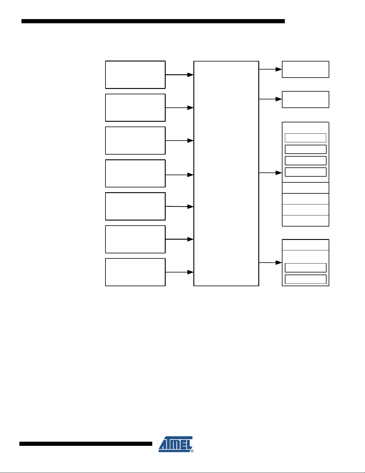
Figure 10-1. Clock system overview
32 MHz
Run-time Calibrated
Internal Oscillator
32 kHz ULP
Internal Oscillator
32.768 kHz
Calibrated Internal
Oscillator
32.768 KHz
Crystal Oscillator
0.4 - 16 MHz
Crystal Oscillator
2 MHz
Run-Time Calibrated
Internal Oscillator
External
Clock Input
CLOCK CONTROL
UNIT
with PLL and
Prescaler
WDT/BOD
clk
ULP
RTC
clk
RTC
EVSYS
PERIPHERALS
ADC
DAC
PORTS
...
clk
PER
DMA
INTERRUPT
RAM
NVM MEMORY
FLASH
EEPROM
CPU
clk
CPU
XMEGA A4
10.3 Clock Options
10.3.1 32 kHz Ultra Low Power Internal Oscillator
Each clock source is briefly described in the following sub-sections.
The 32 kHz Ultra Low Power (ULP) Internal Oscillator is a very low power consumption clock
source. It is used for the Watchdog Timer, Brown-Out Detection and as an asynchronous clock
source for the Real Time Counter. This oscillator cannot be used as the system clock source,
and it cannot be directly controlled from software.
10.3.2 32.768 kHz Calibrated Internal Oscillator
The 32.768 kHz Calibrated Internal Oscillator is a high accuracy clock source that can be used
as the system clock source or as an asynchronous clock source for the Real Time Counter. It is
calibrated during production to provide a default frequency which is close to its nominal
frequency.
8069L–AVR–11/09
19

10.3.3 32.768 kHz Crystal Oscillator
The 32.768 kHz Crystal Oscillator is a low power driver for an external watch crystal. It can be
used as system clock source or as asynchronous clock source for the Real Time Counter.
10.3.4 0.4 - 16 MHz Crystal Oscillator
The 0.4 - 16 MHz Crystal Oscillator is a driver intended for driving both external resonators and
crystals ranging from 400 kHz to 16 MHz.
10.3.5 2 MHz Run-time Calibrated Internal Oscillator
The 2 MHz Run-time Calibrated Internal Oscillator is a high frequency oscillator. It is calibrated
during production to provide a default frequency which is close to its nominal frequency. The
oscillator can use the 32 kHz Calibrated Internal Oscillator or the 32 kHz Crystal Oscillator as a
source for calibrating the frequency run-time to compensate for temperature and voltage drift
hereby optimizing the accuracy of the oscillator.
10.3.6 32 MHz Run-time Calibrated Internal Oscillator
The 32 MHz Run-time Calibrated Internal Oscillator is a high frequency oscillator. It is calibrated
during production to provide a default frequency which is close to its nominal frequency. The
oscillator can use the 32 kHz Calibrated Internal Oscillator or the 32 kHz Crystal Oscillator as a
source for calibrating the frequency run-time to compensate for temperature and voltage drift
hereby optimizing the accuracy of the oscillator.
XMEGA A4
10.3.7 External Clock input
The external clock input gives the possibility to connect a clock from an external source.
10.3.8 PLL with Multiplication factor 1 - 31x
The PLL provides the possibility of multiplying a frequency by any number from 1 to 31. In combination with the prescalers, this gives a wide range of output frequencies from all clock sources.
8069L–AVR–11/09
20

11. Power Management and Sleep Modes
11.1 Features
• 5 sleep modes
–Idle
– Power-down
–Power-save
–Standby
– Extended standby
• Power Reduction registers to disable clocks to unused peripherals
11.2 Overview
The XMEGA A4 provides various sleep modes tailored to reduce power consumption to a minimum. All sleep modes are available and can be entered from Active mode. In Active mode the
CPU is executing application code. The application code decides when and what sleep mode to
enter. Interrupts from enabled peripherals and all enabled reset sources can restore the microcontroller from sleep to Active mode.
In addition, Power Reduction registers provide a method to stop the clock to individual peripherals from software. When this is done, the current state of the peripheral is frozen and there is no
power consumption from that peripheral. This reduces the power consumption in Active mode
and Idle sleep mode.
XMEGA A4
11.3 Sleep Modes
11.3.1 Idle Mode
In Idle mode the CPU and Non-Volatile Memory are stopped, but all peripherals including the
Interrupt Controller, Event System and DMA Controller are kept running. Interrupt requests from
all enabled interrupts will wake the device.
11.3.2 Power-down Mode
In Power-down mode all system clock sources, and the asynchronous Real Time Counter (RTC)
clock source, are stopped. This allows operation of asynchronous modules only. The only interrupts that can wake up the MCU are the Two Wire Interface address match interrupts, and
asynchronous port interrupts, e.g pin change.
11.3.3 Power-save Mode
Power-save mode is identical to Power-down, with one exception: If the RTC is enabled, it will
keep running during sleep and the device can also wake up from RTC interrupts.
11.3.4 Standby Mode
Standby mode is identical to Power-down with the exception that all enabled system clock
sources are kept running, while the CPU, Peripheral and RTC clocks are stopped. This reduces
the wake-up time when external crystals or resonators are used.
8069L–AVR–11/09
21

11.3.5 Extended Standby Mode
Extended Standby mode is identical to Power-save mode with the exception that all enabled
system clock sources are kept running while the CPU and Peripheral clocks are stopped. This
reduces the wake-up time when external crystals or resonators are used.
XMEGA A4
8069L–AVR–11/09
22

12. System Control and Reset
12.1 Features
• Multiple reset sources for safe operation and device reset
– Power-On Reset
– External Reset
– Watchdog Reset
The Watchdog Timer runs from separate, dedicated oscillator
– Brown-Out Reset
Accurate, programmable Brown-Out levels
– PDI reset
– Software reset
• Asynchronous reset
– No running clock in the device is required for reset
• Reset status register
12.2 Resetting the AVR
During reset, all I/O registers are set to their initial values. The SRAM content is not reset. Application execution starts from the Reset Vector. The instruction placed at the Reset Vector should
be an Absolute Jump (JMP) instruction to the reset handling routine. By default the Reset Vector
address is the lowest Flash program memory address, ‘0’, but it is possible to move the Reset
Vector to the first address in the Boot Section.
XMEGA A4
The I/O ports of the AVR are immediately tri-stated when a reset source goes active.
The reset functionality is asynchronous, so no running clock is required to reset the device.
After the device is reset, the reset source can be determined by the application by reading the
Reset Status Register.
12.3 Reset Sources
12.3.1 Power-On Reset
The MCU is reset when the supply voltage VCC is below the Power-on Reset threshold voltage.
12.3.2 External Reset
The MCU is reset when a low level is present on the RESET pin.
12.3.3 Watchdog Reset
The MCU is reset when the Watchdog Timer period expires and the Watchdog Reset is enabled.
The Watchdog Timer runs from a dedicated oscillator independent of the System Clock. For
more details see ”WDT - Watchdog Timer” on page 24.
12.3.4 Brown-Out Reset
The MCU is reset when the supply voltage VCC is below the Brown-Out Reset threshold voltage
and the Brown-out Detector is enabled. The Brown-out threshold voltage is programmable.
8069L–AVR–11/09
23

12.3.5 PDI reset
The MCU can be reset through the Program and Debug Interface (PDI).
12.3.6 Software reset
The MCU can be reset by the CPU writing to a special I/O register through a timed sequence.
13. WDT - Watchdog Timer
13.1 Features
• 11 selectable timeout periods, from 8 ms to 8s.
• Two operation modes
– Standard mode
– Window mode
• Runs from the 1 kHz output of the 32 kHz Ultra Low Power oscillator
• Configuration lock to prevent unwanted changes
13.2 Overview
XMEGA A4
The XMEGA A4 has a Watchdog Timer (WDT). The WDT will run continuously when turned on
and if the Watchdog Timer is not reset within a software configurable time-out period, the microcontroller will be reset. The Watchdog Reset (WDR) instruction must be run by software to reset
the WDT, and prevent microcontroller reset.
The WDT has a Window mode. In this mode the WDR instruction must be run within a specified
period called a window. Application software can set the minimum and maximum limits for this
window. If the WDR instruction is not executed inside the window limits, the microcontroller will
be reset.
A protection mechanism using a timed write sequence is implemented in order to prevent
unwanted enabling, disabling or change of WDT settings.
For maximum safety, the WDT also has an Always-on mode. This mode is enabled by programming a fuse. In Always-on mode, application software can not disable the WDT.
8069L–AVR–11/09
24
14. PMIC - Programmable Multi-level Interrupt Controller
14.1 Features
• Separate interrupt vector for each interrupt
• Short, predictable interrupt response time
• Programmable Multi-level Interrupt Controller
– 3 programmable interrupt levels
– Selectable priority scheme within low level interrupts (round-robin or fixed)
– Non-Maskable Interrupts (NMI)
• Interrupt vectors can be moved to the start of the Boot Section
14.2 Overview
XMEGA A4 has a Programmable Multi-level Interrupt Controller (PMIC). All peripherals can
define three different priority levels for interrupts; high, medium or low. Medium level interrupts
may interrupt low level interrupt service routines. High level interrupts may interrupt both lowand medium level interrupt service routines. Low level interrupts have an optional round robin
scheme to make sure all interrupts are serviced within a certain amount of time.
The built in oscillator failure detection mechanism can issue a Non-Maskable Interrupt (NMI).
XMEGA A4
14.3 Interrupt vectors
When an interrupt is serviced, the program counter will jump to the interrupt vector address. The
interrupt vector is the sum of the peripheral’s base interrupt address and the offset address for
specific interrupts in each peripheral. The base addresses for the XMEGA A4 devices are shown
in Table 14-1. Offset addresses for each interrupt available in the peripheral are described for
each peripheral in the XMEGA A manual. For peripherals or modules that have only one interrupt, the interrupt vector is shown in Table 14-1. The program address is the word address.
Table 14-1. Reset and Interrupt Vectors
Program Address
(Base Address) Source Interrupt Description
0x000 RESET
0x002 OSCF_INT_vect Crystal Oscillator Failure Interrupt vector (NMI)
0x004 PORTC_INT_base Port C Interrupt base
0x008 PORTR_INT_base Port R Interrupt base
0x00C DMA_INT_base DMA Controller Interrupt base
0x014 RTC_INT_base Real Time Counter Interrupt base
0x018 TWIC_INT_base Two-Wire Interface on Port C Interrupt base
0x01C TCC0_INT_base Timer/Counter 0 on port C Interrupt base
0x028 TCC1_INT_base Timer/Counter 1 on port C Interrupt base
0x030 SPIC_INT_vect SPI on port C Interrupt vector
0x032 USARTC0_INT_base USART 0 on port C Interrupt base
0x038 USARTC1_INT_base USART 1 on port C Interrupt base
0x03E AES_INT_vect AES Interrupt vector
8069L–AVR–11/09
25
Table 14-1. Reset and Interrupt Vectors (Continued)
Program Address
(Base Address) Source Interrupt Description
0x040 NVM_INT_base Non-Volatile Memory Interrupt base
0x044 PORTB_INT_base Port B Interrupt base
0x056 PORTE_INT_base Port E Interrupt base
0x05A TWIE_INT_base Two-Wire Interface on Port E Interrupt base
0x05E TCE0_INT_base Timer/Counter 0 on port E Interrupt base
0x06A TCE1_INT_base Timer/Counter 1 on port E Interrupt base
0x074 USARTE0_INT_base USART 0 on port E Interrupt base
0x080 PORTD_INT_base Port D Interrupt base
0x084 PORTA_INT_base Port A Interrupt base
0x088 ACA_INT_base Analog Comparator on Port A Interrupt base
0x08E ADCA_INT_base Analog to Digital Converter on Port A Interrupt base
0x09A TCD0_INT_base Timer/Counter 0 on port D Interrupt base
0x0A6 TCD1_INT_base Timer/Counter 1 on port D Interrupt base
0x0AE SPID_INT_vector SPI on port D Interrupt vector
0x0B0 USARTD0_INT_base USART 0 on port D Interrupt base
XMEGA A4
0x0B6 USARTD1_INT_base USART 1 on port D Interrupt base
8069L–AVR–11/09
26

15. I/O Ports
15.1 Features
15.2 Overview
XMEGA A4
• Selectable input and output configuration for each pin individually
• Flexible pin configuration through dedicated Pin Configuration Register
• Synchronous and/or asynchronous input sensing with port interrupts and events
– Sense both edges
– Sense rising edges
– Sense falling edges
– Sense low level
• Asynchronous wake-up from all input sensing configurations
• Two port interrupts with flexible pin masking
• Highly configurable output driver and pull settings:
– Totem-pole
– Pull-up/-down
– Wired-AND
– Wired-OR
– Bus-keeper
– Inverted I/O
• Optional Slew rate control
• Configuration of multiple pins in a single operation
• Read-Modify-Write (RMW) support
• Toggle/clear/set registers for Output and Direction registers
• Clock output on port pin
• Event Channel 7 output on port pin
• Mapping of port registers (virtual ports) into bit accessible I/O memory space
The XMEGA A4 devices have flexible General Purpose I/O Ports. A port consists of up to 8 pins,
ranging from pin 0 to pin 7. The ports implement several functions, including synchronous/asynchronous input sensing, pin change interrupts and configurable output settings. All functions are
individual per pin, but several pins may be configured in a single operation.
15.3 I/O configuration
All port pins (Pn) have programmable output configuration. In addition, all port pins have an
inverted I/O function. For an input, this means inverting the signal between the port pin and the
pin register. For an output, this means inverting the output signal between the port register and
the port pin. The inverted I/O function can be used also when the pin is used for alternate
functions.
8069L–AVR–11/09
27
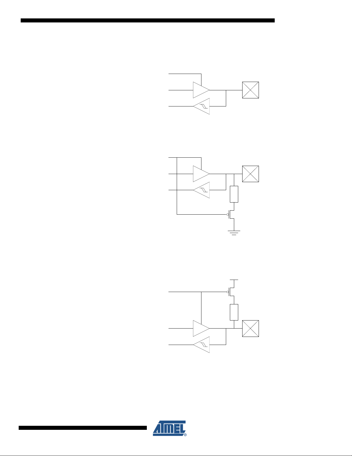
15.3.1 Push-pull
INn
OUTn
DIRn
Pn
INn
OUTn
DIRn
Pn
INn
OUTn
DIRn
Pn
15.3.2 Pull-down
XMEGA A4
Figure 15-1. I/O configuration - Totem-pole
Figure 15-2. I/O configuration - Totem-pole with pull-down (on input)
15.3.3 Pull-up
15.3.4 Bus-keeper
Figure 15-3. I/O configuration - Totem-pole with pull-up (on input)
The bus-keeper’s weak output produces the same logical level as the last output level. It acts as
a pull-up if the last level was ‘1’, and pull-down if the last level was ‘0’.
8069L–AVR–11/09
28
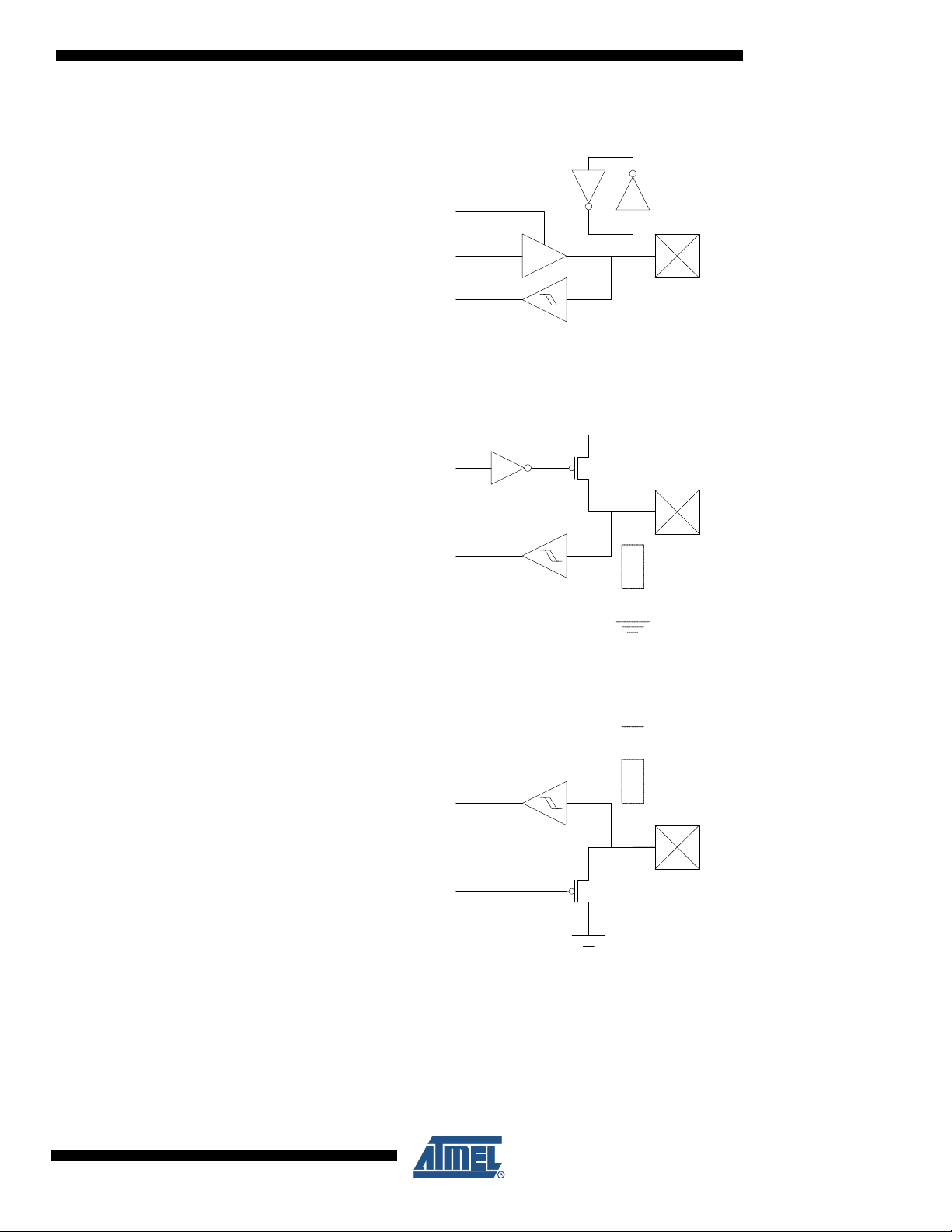
15.3.5 Others
INn
OUTn
DIRn
Pn
INn
OUTn
Pn
INn
OUTn
Pn
XMEGA A4
Figure 15-4. I/O configuration - Totem-pole with bus-keeper
Figure 15-5. Output configuration - Wired-OR with optional pull-down
8069L–AVR–11/09
Figure 15-6. I/O configuration - Wired-AND with optional pull-up
29
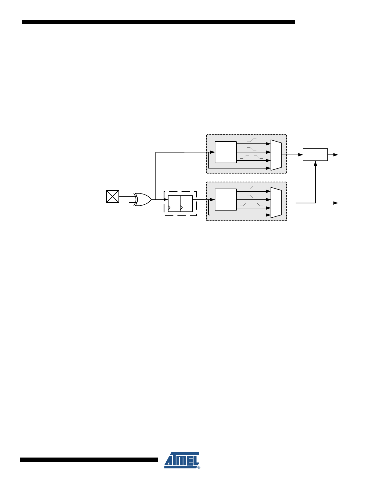
15.4 Input sensing
INVERTED I/O
Interrupt
Control
IREQ
Event
Pn
D
Q
R
D
Q
R
Synchronizer
INn
EDGE
DETECT
Asynchronous sensing
Synchronous sensing
EDGE
DETECT
XMEGA A4
• Sense both edges
• Sense rising edges
• Sense falling edges
• Sense low level
Input sensing is synchronous or asynchronous depending on the enabled clock for the ports,
and the configuration is shown in Figure 15-7 on page 30.
Figure 15-7. Input sensing system overview
When a pin is configured with inverted I/O, the pin value is inverted before the input sensing.
15.5 Port Interrupt
Each port has two interrupts with separate priority and interrupt vector. All pins on the port can
be individually selected as source for each of the interrupts. The interrupts are then triggered
according to the input sense configuration for each pin configured as source for the interrupt.
15.6 Alternate Port Functions
In addition to the input/output functions on all port pins, most pins have alternate functions. This
means that other modules or peripherals connected to the port can use the port pins for their
functions, such as communication or pulse-width modulation. ”Pinout and Pin Functions” on
page 49 shows which modules on peripherals that enable alternate functions on a pin, and
which alternate function is available on a pin.
8069L–AVR–11/09
30

16. T/C - 16-bit Timer/Counter
16.1 Features
• Five 16-bit Timer/Counters
– Three Timer/Counters of type 0
– Two Timer/Counters of type 1
• Three Compare or Capture (CC) Channels in Timer/Counter 0
• Two Compare or Capture (CC) Channels in Timer/Counter 1
• Double Buffered Timer Period Setting
• Double Buffered Compare or Capture Channels
• Waveform Generation:
– Single Slope Pulse Width Modulation
– Dual Slope Pulse Width Modulation
– Frequency Generation
• Input Capture:
– Input Capture with Noise Cancelling
– Frequency capture
– Pulse width capture
– 32-bit input capture
• Event Counter with Direction Control
• Timer Overflow and Timer Error Interrupts and Events
• One Compare Match or Capture Interrupt and Event per CC Channel
• Supports DMA Operation
• Hi-Resolution Extension (Hi-Res)
• Advanced Waveform Extension (AWEX)
XMEGA A4
16.2 Overview
XMEGA A4 has five Timer/Counters, three Timer/Counter 0 and two Timer/Counter 1. The difference between them is that Timer/Counter 0 has four Compare/Capture channels, while
Timer/Counter 1 has two Compare/Capture channels.
The Timer/Counters (T/C) are 16-bit and can count any clock, event or external input in the
microcontroller. A programmable prescaler is available to get a useful T/C resolution. Updates of
Timer and Compare registers are double buffered to ensure glitch free operation. Single slope
PWM, dual slope PWM and frequency generation waveforms can be generated using the Compare Channels.
Through the Event System, any input pin or event in the microcontroller can be used to trigger
input capture, hence no dedicated pins are required for this. The input capture has a noise canceller to avoid incorrect capture of the T/C, and can be used to do frequency and pulse width
measurements.
A wide range of interrupt or event sources are available, including T/C Overflow, Compare
match and Capture for each Compare/Capture channel in the T/C.
PORTC and PORTD each has one Timer/Counter 0 and one Timer/Counter1. PORTE has one
Timer/Conter0. Notation of these are TCC0 (Time/Counter C0), TCC1, TCD0, TCD1 and TCE0,
respectively.
8069L–AVR–11/09
31

XMEGA A4
AWeX
Compare/Capture Channel D
Compare/Capture Channel C
Compare/Capture Channel B
Compare/Capture Channel A
Waveform
Generation
Buffer
Comparator
Hi-Res
Fault
Protection
Capture
Control
Base Counter
Counter
Control Logic
Timer Period
Prescaler
DTI
Dead-Time
Insertion
Pattern
Generation
clk
PER4
PORT
Event
System
clk
PER
Timer/Counter
Figure 16-1. Overview of a Timer/Counter and closely related peripherals
The Hi-Resolution Extension can be enabled to increase the waveform generation resolution by
2 bits (4x). This is available for all Timer/Counters. See ”Hi-Res - High Resolution Extension” on
page 34 for more details.
The Advanced Waveform Extension can be enabled to provide extra and more advanced feature for the Timer/Counter. This is only available for Timer/Counter 0. See ”AWEX - Advanced
Waveform Extension” on page 33 for more details.
8069L–AVR–11/09
32

17. AWEX - Advanced Waveform Extension
17.1 Features
• Output with complementary output from each Capture channel
• Four Dead Time Insertion (DTI) Units, one for each Capture channel
• 8-bit DTI Resolution
• Separate High and Low Side Dead-Time Setting
• Double Buffered Dead-Time
• Event Controlled Fault Protection
• Single Channel Multiple Output Operation (for BLDC motor control)
• Double Buffered Pattern Generation
17.2 Overview
The Advanced Waveform Extension (AWEX) provides extra features to the Timer/Counter in
Waveform Generation (WG) modes. The AWEX enables easy and safe implementation of for
example, advanced motor control (AC, BLDC, SR, and Stepper) and power control applications.
Any WG output from a Timer/Counter 0 is split into a complimentary pair of outputs when any
AWEX feature is enabled. These output pairs go through a Dead-Time Insertion (DTI) unit that
enables generation of the non-inverted Low Side (LS) and inverted High Side (HS) of the WG
output with dead time insertion between LS and HS switching. The DTI output will override the
normal port value according to the port override setting. Optionally the final output can be
inverted by using the invert I/O setting for the port pin.
XMEGA A4
The Pattern Generation unit can be used to generate a synchronized bit pattern on the port it is
connected to. In addition, the waveform generator output from Compare Channel A can be distributed to, and override all port pins. W hen the Pattern Generator unit is enabled, the DTI unit is
bypassed.
The Fault Protection unit is connected to the Event System. This enables any event to trigger a
fault condition that will disable the AWEX output. Several event channels can be used to trigger
fault on several different conditions.
The AWEX is available for TCC0. The notation of this is AWEXC.
8069L–AVR–11/09
33

18. Hi-Res - High Resolution Extension
18.1 Features
• Increases Waveform Generator resolution by 2-bits (4x)
• Supports Frequency, single- and dual-slope PWM operation
• Supports the AWEX when this is enabled and used for the same Timer/Counter
18.2 Overview
The Hi-Resolution (Hi-Res) Extension is able to increase the resolution of the waveform generation output by a factor of 4. When enabled for a Timer/Counter, the Fast Peripheral clock running
at four times the CPU clock speed will be as input to the Timer/Counter.
The High Resolution Extension can also be used when an AWEX is enabled and used with a
Timer/Counter.
XMEGA A4 devices have three Hi-Res Extensions that each can be enabled for each
Timer/Counters pair on PORTC, PORTD and PORTE. The notation of these are HIRESC,
HIRESD and HIRESE, respectively.
XMEGA A4
8069L–AVR–11/09
34

19. RTC - 16-bit Real-Time Counter
10-bit
prescaler
Counter
Period
Compare
=
=
Overflow
Compare Match
1 kHz
32 kHz
19.1 Features
• 16-bit Timer
• Flexible Tick resolution ranging from 1 Hz to 32.768 kHz
• One Compare register
• One Period register
• Clear timer on Overflow or Compare Match
• Overflow or Compare Match event and interrupt generation
19.2 Overview
The XMEGA A4 includes a 16-bit Real-time Counter (RTC). The RTC can be clocked from an
accurate 32.768 kHz Crystal Oscillator, the 32.768 kHz Calibrated Internal Oscillator, or from the
32 kHz Ultra Low Power Internal Oscillator. The RTC includes both a Period and a Compare
register. For details, see Figure 19-1.
A wide range of Resolution and Time-out periods can be configured using the RTC. With a maximum resolution of 30.5 µs, time-out periods range up to 2000 seconds. With a resolution of 1
second, the maximum time-out period is over 18 hours (65536 seconds).
XMEGA A4
Figure 19-1. Real Time Counter overview
8069L–AVR–11/09
35

20. TWI - Two-Wire Interface
20.1 Features
• Two Identical TWI peripherals
• Simple yet Powerful and Flexible Communication Interface
• Both Master and Slave Operation Supported
• Device can Operate as Transmitter or Receiver
• 7-bit Address Space Allows up to 128 Different Slave Addresses
• Multi-master Arbitration Support
• Up to 400 kHz Data Transfer Speed
• Slew-rate Limited Output Drivers
• Noise Suppression Circuitry Rejects Spikes on Bus Lines
• Fully Programmable Slave Address with General Call Support
• Address Recognition Causes Wake-up when in Sleep Mode
2
• I
C and System Management Bus (SMBus) compatible
20.2 Overview
The Two-Wire Interface (TWI) is a bi-directional wired-AND bus with only two lines, the clock
(SCL) line and the data (SDA) line. The protocol makes it possible to interconnect up to 128 individually addressable devices. Since it is a multi-master bus, one or more devices capable of
taking control of the bus can be connected.
XMEGA A4
The only external hardware needed to implement the bus is a single pull-up resistor for each of
the TWI bus lines. Mechanisms for resolving bus contention are inherent in the TWI protocol.
PORTC and PORTE each has one TWI. Notation of these peripherals are TWIC and TWIE,
respectively.
8069L–AVR–11/09
36

21. SPI - Serial Peripheral Interface
21.1 Features
• Two Identical SPI peripherals
• Full-duplex, Three-wire Synchronous Data Transfer
• Master or Slave Operation
• LSB First or MSB First Data Transfer
• Seven Programmable Bit Rates
• End of Transmission Interrupt Flag
• Write Collision Flag Protection
• Wake-up from Idle Mode
• Double Speed (CK/2) Master SPI Mode
21.2 Overview
The Serial Peripheral Interface (SPI) allows high-speed full-duplex, synchronous data transfer
between different devices. Devices can communicate using a master-slave scheme, and data is
transferred both to and from the devices simultaneously.
PORTC and PORTD each has one SPI. Notation of these peripherals are SPIC and SPID,
respectively.
XMEGA A4
8069L–AVR–11/09
37

22. USART
22.1 Features
22.2 Overview
XMEGA A4
• Five Identical USART peripherals
• Full Duplex Operation (Independent Serial Receive and Transmit Registers)
• Asynchronous or Synchronous Operation
• Master or Slave Clocked Synchronous Operation
• High-resolution Arithmetic Baud Rate Generator
• Supports Serial Frames with 5, 6, 7, 8, or 9 Data Bits and 1 or 2 Stop Bits
• Odd or Even Parity Generation and Parity Check Supported by Hardware
• Data OverRun Detection
• Framing Error Detection
• Noise Filtering Includes False Start Bit Detection and Digital Low Pass Filter
• Three Separate Interrupts on TX Complete, TX Data Register Empty and RX Complete
• Multi-processor Communication Mode
• Double Speed Asynchronous Communication Mode
• Master SPI mode for SPI communication
• IrDA support through the IRCOM module
The Universal Synchronous and Asynchronous serial Receiver and Transmitter (USART) is a
highly flexible serial communication module. The USART supports full duplex communication,
and both asynchronous and clocked synchronous operation. The USART can also be set in
Master SPI mode to be used for SPI communication.
Communication is frame based, and the frame format can be customized to support a wide
range of standards. The USART is buffered in both direction, enabling continued data transmission without any delay between frames. There are separate interrupt vectors for receive and
transmit complete, enabling fully interrupt driven communication. Frame error and buffer overflow are detected in hardware and indicated with separate status flags. Even or odd parity
generation and parity check can also be enabled.
One USART can use the IRCOM module to support IrDA 1.4 physical compliant pulse modulation and demodulation for baud rates up to 115.2 kbps.
PORTC and PORTD each has two USARTs. PORTE has one USART. Notation of these peripherals are USARTC0, USARTC1, USARTD0, USARTD1 and USARTE0, respectively.
8069L–AVR–11/09
38

23. IRCOM - IR Communication Module
23.1 Features
• Pulse modulation/demodulation for infrared communication
• Compatible to IrDA 1.4 physical for baud rates up to 115.2 kbps
• Selectable pulse modulation scheme
– 3/16 of baud rate period
– Fixed pulse period, 8-bit programmable
– Pulse modulation disabled
• Built in filtering
• Can be connected to and used by one USART at a time
23.2 Overview
XMEGA contains an Infrared Communication Module (IRCOM) for IrDA communication with
baud rates up to 115.2 kbps. This supports three modulation schemes: 3/16 of baud rate period,
fixed programmable pulse time based on the Peripheral Clock speed, or pulse modulation disabled. There is one IRCOM available which can be connected to any USART to enable infrared
pulse coding/decoding for that USART.
XMEGA A4
8069L–AVR–11/09
39

24. Crypto Engine
24.1 Features
24.2 Overview
XMEGA A4
• Data Encryption Standard (DES) CPU instruction
• Advanced Encryption Standard (AES) Crypto module
• DES Instruction
– Encryption and Decryption
– Single-cycle DES instruction
– Encryption/Decryption in 16 clock cycles per 8-byte block
• AES Crypto Module
– Encryption and Decryption
– Support 128-bit keys
– Support XOR data load mode to the State memory for Cipher Block Chaining
– Encryption/Decryption in 375 clock cycles per 16-byte block
The Advanced Encryption Standard (AES) and Data Encryption Standard (DES) are two commonly used encryption standards. These are supported through an AES peripheral module and
a DES CPU instruction. All communication interfaces and the CPU can optionally use AES and
DES encrypted communication and data storage.
DES is supported by a DES instruction in the AVR XMEGA CPU. The 8-byte key and 8-byte
data blocks must be loaded into the Register file, and then DES must be executed 16 times to
encrypt/decrypt the data block.
The AES Crypto Module encrypts and decrypts 128-bit data blocks with the use of a 128-bit key.
The key and data must be loaded into the key and state memory in the module before encryption/decryption is started. It takes 375 peripheral clock cycles before the encryption/decryption is
done and decrypted/encrypted data can be read out, and an optional interrupt can be generated.
The AES Crypto Module also has DMA support with transfer triggers when encryption/decryption is done and optional auto-start of encryption/decryption when the state memory is fully
loaded.
8069L–AVR–11/09
40

25. ADC - 12-bit Analog to Digital Converter
25.1 Features
• One ADC with 12-bit resolution
• 2 Msps sample rate
• Signed and Unsigned conversions
• 4 result registers with individual input channel control
• 12 single ended inputs
• 8x4 differential inputs
• 4 internal inputs:
– Integrated Temperature Sensor
– DAC Output
– VCC voltage divided by 10
– Bandgap voltage
• Software selectable gain of 2, 4, 8, 16, 32 or 64
• Selectable accuracy of 8- or 12-bit.
• Internal or External Reference selection
• Event triggered conversion for accurate timing
• DMA transfer of conversion results
• Interrupt/Event on compare result
25.2 Overview
XMEGA A4
XMEGA A4 devices have one Analog to Digital Converter (ADC), see Figure 25-1 on page 42.
The ADC converts analog voltages to digital values. The ADC has 12-bit resolution and is capable of converting up to 2 million samples per second. The input selection is flexible, and both
single-ended and differential measurements can be done. For differential measurements an
optional gain stage is available to increase the dynamic range. In addition several internal signal
inputs are available. The ADC can provide both signed and unsigned results.
This is a pipeline ADC. A pipeline ADC consists of several consecutive stages, where each
stage convert one part of the result. The pipeline design enables high sample rate at low clock
speeds, and remove limitations on samples speed versus propagation delay. This also means
that a new analog voltage can be sampled and a new ADC measurement started while other
ADC measurements are ongoing.
ADC measurements can either be started by application software or an incoming event from
another peripheral in the device. Four different result registers with individual input selection
(MUX selection) are provided to make it easier for the application to keep track of the data. Each
result register and MUX selection pair is referred to as an ADC Channel. It is possible to use
DMA to move ADC results directly to memory or peripherals when conversions are done.
Both internal and external analog reference voltages can be used. An accurate internal 1.0V
reference is available.
An integrated temperature sensor is available and the output from this can be measured with the
ADC. The output from the DAC, VCC/10 and the Bandgap voltage can also be measured by the
ADC.
8069L–AVR–11/09
41

Figure 25-1. ADC overview
ADC
Channel A
Register
Channel B
Register
Channel C
Register
Channel D
Register
Pin inputsPin inputs
1-64 X
Internal inputs
Channel A MUX selection
Channel B MUX selection
Channel C MUX selection
Channel D MUX selection
Event
Trigger
Configuration
Reference selection
XMEGA A4
Each ADC has four MUX selection registers with a corresponding result register. This means
that four channels can be sampled within 1.5 µs without any intervention by the application other
than starting the conversion. The results will be available in the result registers.
The ADC may be configured for 8- or 12-bit resolution, reducing the minimum conversion time
(propagation delay) from 3.5 µs for 12-bit to 2.5 µs for 8-bit resolution.
ADC conversion results are provided left- or right adjusted with optional ‘1’ or ‘0’ padding. This
eases calculation when the result is represented as a signed integer (signed 16-bit number).
PORTA has one ADC. Notation of this peripheral is ADCA.
8069L–AVR–11/09
42

26. DAC - 12-bit Digital to Analog Converter
DAC
Channel A
Register
Channel B
Register
Event
Trigger
Configuration
Reference selection
Channel A
Channel B
26.1 Features
• One DAC with 12-bit resolution
• Up to 1 Msps conversion rate
• Flexible conversion range
• Multiple trigger sources
• 1 continuous output or 2 Sample and Hold (S/H) outputs
• Built-in offset and gain calibration
• High drive capabilities
• Low Power Mode
26.2 Overview
The XMEGA A4 devices feature one 12-bit, 1 Msps DAC with built-in offset and gain calibration,
see Figure 26-1 on page 43.
A DAC converts a digital value into an analog signal. The DAC may use an internal 1.1 voltage
as the upper limit for conversion, but it is also possible to use the supply voltage or any applied
voltage in-between. The external reference input is shared with the ADC reference input.
XMEGA A4
Figure 26-1. DAC overview
The DAC has one continuous output with high drive capabilities for both resistive and capacitive
loads. It is also possible to split the continuous time channel into two Sample and Hold (S/H)
channels, each with separate data conversion registers.
A DAC conversion may be started from the application software by writing the data conversion
registers. The DAC can also be configured to do conversions triggered by the Event System to
have regular timing, independent of the application software. DMA may be used for transferring
data from memory locations to DAC data registers.
The DAC has a built-in calibration system to reduce offset and gain error when loading with a
calibration value from software.
8069L–AVR–11/09
PORTB has one DAC. Notation of this peripheral is DACB.
43

27. AC - Analog Comparator
27.1 Features
• Two Analog Comparators
• Selectable Power vs. Speed
• Selectable hysteresis
– 0, 20 mV, 50 mV
• Analog Comparator output available on pin
• Flexible Input Selection
– All pins on the port
– Output from the DAC
– Bandgap reference voltage.
– Voltage scaler that can perform a 64-level scaling of the internal VCC voltage.
• Interrupt and event generation on
– Rising edge
– Falling edge
–Toggle
• Window function interrupt and event generation on
– Signal above window
– Signal inside window
– Signal below window
27.2 Overview
XMEGA A4
XMEGA A4 features two Analog Comparators (AC). An Analog Comparator compares two voltages, and the output indicates which input is largest. The Analog Comparator may be configured
to give interrupt requests and/or events upon several different combinations of input change.
Both hysteresis and propagation delays may be adjusted in order to find the optimal operation
for each application.
A wide range of input selection is available, both external pins and several internal signals can
be used.
The Analog Comparators are always grouped in pairs (AC0 and AC1) on each analog port. They
have identical behavior but separate control registers.
Optionally, the state of the comparator is directly available on a pin.
PORTA has one AC pair. Notation of this peripheral is ACA.
8069L–AVR–11/09
44

Figure 27-1. Analog comparator overview
AC0
+
-
Pin inputs
Internal inputs
Pin inputs
Internal inputs
VCC scaled
Interrupt
sensitivity
control
Interrupts
AC1
+
-
Pin inputs
Internal inputs
Pin inputs
Internal inputs
VCC scaled
Events
Pin 0 output
XMEGA A4
8069L–AVR–11/09
45

27.3 Input Selection
AC0
+
-
AC1
+
-
Input signal
Upper limit of window
Lower limit of window
Interrupt
sensitivity
control
Interrupts
Events
The Analog comparators have a very flexible input selection and the two comparators grouped
in a pair may be used to realize a window function. One pair of analog comparators is shown in
Figure 27-1 on page 45.
•
Input selection from pin
• Internal signals available on positive analog comparator inputs
• Internal signals available on negative analog comparator inputs
27.4 Window Function
The window function is realized by connecting the external inputs of the two analog comparators
in a pair as shown in Figure 27-2.
XMEGA A4
– Pin 0, 1, 2, 3, 4, 5, 6 selectable to positive input of analog comparator
– Pin 0, 1, 3, 5, 7 selectable to negative input of analog comparator
– Output from 12-bit DAC
– 64-level scaler of the VCC, available on negative analog comparator input
– Bandgap voltage reference
– Output from 12-bit DAC
Figure 27-2. Analog comparator window function
8069L–AVR–11/09
46

28. OCD - On-chip Debug
28.1 Features
• Complete Program Flow Control
– Go, Stop, Reset, Step into, Step over, Step out, Run-to-Cursor
• Debugging on C and high-level language source code level
• Debugging on Assembler and disassembler level
• 1 dedicated program address or source level breakpoint for AVR Studio / debugger
• 4 Hardware Breakpoints
• Unlimited Number of User Program Breakpoints
• Unlimited Number of User Data Breakpoints, with break on:
– Data location read, write or both read and write
– Data location content equal or not equal to a value
– Data location content is greater or less than a value
– Data location content is within or outside a range
– Bits of a data location are equal or not equal to a value
• Non-Intrusive Operation
– No hardware or software resources in the device are used
• High Speed Operation
– No limitation on debug/programming clock frequency versus system clock frequency
28.2 Overview
XMEGA A4
The XMEGA A4 has a powerful On-Chip Debug (OCD) system that - in combination with Atmel’s
development tools - provides all the necessary functions to debug an application. It has support
for program and data breakpoints, and can debug an application from C and high level language
source code level, as well as assembler and disassembler level. It has full Non-Intrusive Operation and no hardware or software resources in the device are used. The ODC system is
accessed through an external debugging tool which connects to the PDI physical interface.
Refer to ”Program and Debug Interfaces” on page 48.
8069L–AVR–11/09
47

29. Program and Debug Interfaces
29.1 Features
• PDI - Program and Debug Interface (Atmel proprietary 2-pin interface)
• Access to the OCD system
• Programming of Flash, EEPROM, Fuses and Lock Bits
29.2 Overview
The programming and debug facilities are accessed through PDI physical interface. The PDI
physical interface uses one dedicated pin together with the Reset pin, and no general purpose
pins are used.
29.3 PDI - Program and Debug Interface
The PDI is an Atmel proprietary protocol for communication between the microcontroller and
Atmel’s development tools.
XMEGA A4
8069L–AVR–11/09
48

30. Pinout and Pin Functions
The pinout of XMEGA A4 is shown in ”Pinout/Block Diagram” on page 3. In addition to general
I/O functionality, each pin may have several functions. This will depend on which peripheral is
enabled and connected to the actual pin. Only one of the alternate pin functions can be used at
time.
30.1 Alternate Pin Functions Description
The tables below shows the notation for all pin functions available and describe their functions.
30.1.1 Operation/Power Supply
VCC Digital supply voltage
AVCC Analog supply voltage
GND Ground
30.1.2 Port Interrupt functions
SYNC Port pin with full synchronous and limited asynchronous interrupt function
ASYNC Port pin with full synchronous and full asynchronous interrupt function
XMEGA A4
30.1.3 Analog functions
ACn Analog Comparator input pin n
AC0OUT Analog Comparator 0 Output
ADCn Analog to Digital Converter input pin n
DACn Digital to Analog Converter output pin n
AREF Analog Reference input pin
30.1.4 Timer/Counter and AWEX functions
OCnx Output Compare Channel x for Timer/Counter n
OCnx
Inverted Output Compare Channel x for Timer/Counter n
8069L–AVR–11/09
49

30.1.5 Communication functions
SCL Serial Clock for TWI
SDA Serial Data for TWI
XCKn Transfer Clock for USART n
RXDn Receiver Data for USART n
TXDn Transmitter Data for USART n
SS
MOSI Master Out Slave In for SPI
MISO Master In Slave Out for SPI
SCK Serial Clock for SPI
30.1.6 Oscillators, Clock and Event
TOSCn Timer Oscillator pin n
XTALn Input/Output for inverting Oscillator pin n
XMEGA A4
Slave Select for SPI
30.1.7 Debug/System functions
RESET
PDI_CLK Program and Debug Interface Clock pin
PDI_DATA Program and Debug Interface Data pin
Reset pin
8069L–AVR–11/09
50

XMEGA A4
30.2 Alternate Pin Functions
The tables below shows the main and alternate pin functions for all pins on each port. It also
shows which peripheral which make use of or enable the alternate pin function.
Table 30-1. Port A - Alternate functions
PORTA PIN # INTERRUPT ADCA POS ADCA NEG
GND 38
AVC C 39
PA0 40 SYNC ADC0 ADC0 ADC0 AC0 AC0 AREF
PA1 41 SYNC ADC1 ADC1 ADC1 AC1 AC1
PA2 42 SYNC/ASYNC ADC2 ADC2 ADC2 AC2
PA3 43 SYNC ADC3 ADC3 ADC3 AC3 AC3
PA4 44 SYNC ADC4 ADC4 ADC4 AC4
PA5 1 SYNC ADC5 ADC5 ADC5 AC5 AC5
PA6 2 SYNC ADC6 ADC6 ADC6 AC6
PA7 3 SYNC ADC7 ADC7 ADC7 AC7 AC0 OUT
ADCA
GAINPOS
ADCA
GAINNEG ACA POS ACA NEG ACA OUT REF
Table 30-2. Port B - Alternate functions
PORTB PIN # INTERRUPT ADCA POS DACB REF
PB0 4SYNCADC8 AREF
PB1 5SYNCADC9
PB2 6 SYNC/ASYNC ADC10 DAC0
PB3 7 SYNC ADC11 DAC1
Table 30-3. Port C - Alternate functions
PORTC PIN # INTERRUPT TCC0 AWEXC TCC1 USARTC0 USARTC1 SPI TWIC CLOCKOUT EVENTOUT
GND 8
VCC 9
PC0 10 SYNC OC0A OC0A
PC1 11 SYNC OC0B OC0A XCK0 SCL
PC2 12 SYNC/ASYNC OC0C OC0B RXD0
PC3 13 SYNC OC0D OC0B TXD0
PC4 14 SYNC OC0C OC1A SS
PC5 15 SYNC OC0C OC1B XCK1 MOSI
PC6 16 SYNC OC0D
PC7 17 SYNC OC0D TXD1 SCK CLKOUT EVOUT
RXD1 MISO
SDA
8069L–AVR–11/09
51

XMEGA A4
Table 30-4. Port D - Alternate functions
PORTD PIN # INTERRUPT TCD0 TCD1 USARTD0 USARTD1 SPID CLOCKOUT EVENTOUT
GND 18
VCC 19
PD0 20 SYNC OC0A
PD1 21 SYNC OC0B XCK0
PD2 22 SYNC/ASYNC OC0C RXD0
PD3 23 SYNC OC0D TXD0
PD4 24 SYNC OC1A SS
PD5 25 SYNC OC1B XCK1 MOSI
PD6 26 SYNC RXD1 MISO
PD7 27 SYNC TXD1 SCK CLKOUT EVOUT
Table 30-5. Port E - Alternate functions
PORT E PIN # INTERRUPT TCE0 USARTE0 TWIE
PE0 28 SYNC OC0A SDA
PE1 29 SYNC OC0B XCK0 SCL
GND 30
VCC 31
PE2 32 SYNC/ASYNC OC0C RXD0
PE3 33 SYNC OC0D TXD0
Table 30-6. Port R - Alternate functions
PORTR PIN # XTAL PDI TOSC
PDI 34 PDI_DATA
RESET 35 PDI_CLK
PR0 36 XTAL2 TOSC 2
PR1 37 XTAL1 TOSC 1
8069L–AVR–11/09
52

31. Peripheral Module Address Map
The address maps show the base address for each peripheral and module in XMEGA A4. For
complete register description and summary for each peripheral module, refer to the XMEGA A
Manual.
Base Address Name Description
0x0000 GPIO General Purpose IO Registers
0x0010 VPORT0 Virtual Port 0
0x0014 VPORT1 Virtual Port 1
0x0018 VPORT2 Virtual Port 2
0x001C VPORT3 Virtual Port 2
0x0030 CPU CPU
0x0040 CLK Clock Control
0x0048 SLEEP Sleep Controller
0x0050 OSC Oscillator Control
0x0060 DFLLRC32M DFLL for the 32 MHz Internal RC Oscillator
0x0068 DFLLRC2M DFLL for the 2 MHz RC Oscillator
0x0070 PR Power Reduction
0x0078 RST Reset Controller
0x0080 WDT Watch-Dog Timer
0x0090 MCU MCU Control
0x00A0 PMIC Programmable MUltilevel Interrupt Controller
0x00B0 PORTCFG Port Configuration
0x00C0 AES AES Module
0x0100 DMA DMA Controller
0x0180 EVSYS Event System
0x01C0 NVM Non Volatile Memory (NVM) Controller
0x0200 ADCA Analog to Digital Converter on port A
0x0320 DACB Digital to Analog Converter on port B
0x0380 ACA Analog Comparator pair on port A
0x0400 RTC Real Time Counter
0x0480 TWIC Two Wire Interface on port C
0x04A0 TWIE Two Wire Interface on port E
0x0600 PORTA Port A
0x0620 PORTB Port B
0x0640 PORTC Port C
0x0660 PORTD Port D
0x0680 PORTE Port E
0x07E0 PORTR Port R
0x0800 TCC0 Timer/Counter 0 on port C
0x0840 TCC1 Timer/Counter 1 on port C
0x0880 AWEXC Advanced Waveform Extension on port C
0x0890 HIRESC High Resolution Extension on port C
0x08A0 USARTC0 USART 0 on port C
0x08B0 USARTC1 USART 1 on port C
0x08C0 SPIC Serial Peripheral Interface on port C
0x08F8 IRCOM Infrared Communication Module
0x0900 TCD0 Timer/Counter 0 on port D
0x0940 TCD1 Timer/Counter 1 on port D
0x0990 HIRESD High Resolution Extension on port D
0x09A0 USARTD0 USART 0 on port D
0x09B0 USARTD1 USART 1 on port D
0x09C0 SPID Serial Peripheral Interface on port D
0x0A00 TCE0 Timer/Counter 0 on port E
0x0A90 HIRESE High Resolution Extension on port E
0x0AA0 USARTE0 USART 0 on port E
XMEGA A4
8069L–AVR–11/09
53

XMEGA A4
32. Instruction Set Summary
Mnemonics Operands Description Operation Flags #Clocks
Arithmetic and Logic Instructions
ADD Rd, Rr Add without Carry Rd ← Rd + Rr Z,C,N,V,S,H 1
ADC Rd, Rr Add with Carr y Rd ← Rd + Rr + C Z,C,N,V,S,H 1
ADIW Rd, K Add Immediate to Word Rd ← Rd + 1:Rd + K Z,C,N,V,S 2
SUB Rd, Rr Subtract without Carry Rd ← Rd - Rr Z,C,N,V,S,H 1
SUBI Rd, K Subtract Immediate Rd ← Rd - K Z,C,N,V,S,H 1
SBC Rd, Rr Subtract with Carry Rd ← Rd - Rr - C Z,C,N,V,S,H 1
SBCI Rd, K Subtract Immediate with Carry Rd ← Rd - K - C Z,C,N,V,S,H 1
SBIW Rd, K Subtract Immediate from Word Rd + 1:Rd ← Rd + 1:Rd - K Z,C,N,V,S 2
AND Rd, Rr Logical AND Rd ← Rd • Rr Z,N,V,S 1
ANDI Rd, K Logical AND with Immediate Rd ← Rd • K Z,N,V,S 1
OR Rd, Rr Logical OR Rd ← Rd v Rr Z,N,V,S 1
ORI Rd, K Logical OR with Immediate Rd ← Rd v K Z,N,V,S 1
EOR Rd, Rr Exclusive OR Rd ← Rd ⊕ Rr Z,N,V,S 1
COM Rd One’s Complement Rd ← $FF - Rd Z,C,N,V,S 1
NEG Rd Two’s Complement Rd ← $00 - Rd Z,C,N,V,S,H 1
SBR Rd,K Set Bit(s) in Register Rd ← Rd v K Z,N,V,S 1
CBR Rd,K Clear Bit(s) in Register Rd ← Rd • ($FFh - K) Z,N,V,S 1
INC Rd Increment Rd ← Rd + 1 Z,N,V,S 1
DEC Rd Decrement Rd ← Rd - 1 Z,N,V,S 1
TST Rd Test for Zero or Minus Rd ← Rd • Rd Z,N,V,S 1
CLR Rd Clear Register Rd ← Rd ⊕ Rd Z,N,V,S 1
SER Rd Set Register Rd ← $FF None 1
MUL Rd,Rr Multiply Unsigned R1:R0 ← Rd x Rr (UU) Z,C 2
MULS Rd,Rr Multiply Signed R1:R0 ← Rd x Rr (SS) Z,C 2
MULSU Rd,Rr Multiply Signed with Unsigned R1:R0 ← Rd x Rr (SU) Z,C 2
FMUL Rd,Rr Fractional Multiply Unsigned R1:R0 ← Rd x Rr<<1 (UU) Z,C 2
FMULS Rd,Rr Fractional Multiply Signed R1:R0
FMULSU Rd,Rr Fractional Multiply Signed with Unsigned R1:R0 ← Rd x Rr<<1 (SU) Z,C 2
DES K Data Encryption if (H = 0) then R15:R0
RJMP k Relative Jump PC ← PC + k + 1 None 2
IJMP Indirect Jump to (Z) PC(15:0)
EIJMP Extended Indirect Jump to (Z) PC(15:0)
JMP k Jump PC ← k None 3
RCALL k Relative Call Subroutine PC ← PC + k + 1 None 2 / 3
ICALL Indirect Call to (Z) PC(15:0)
EICALL Extended Indirect Call to (Z) PC(15:0)
else if (H = 1) then R15:R0←←
Branch Instructions
PC(21:16)←←Z,0
PC(21:16)←←Z,EIND
PC(21:16)←←Z,0
PC(21:16)←←Z,EIND
← Rd x Rr<<1 (SS) Z,C 2
Encrypt(R15:R0, K)
Decrypt(R15:R0, K)
None 2
None 2
None 2 / 3
None 3
1/2
(1)
(1)
(1)
8069L–AVR–11/09
54

XMEGA A4
Mnemonics Operands Description Operation Flags #Clocks
CALL k call Subroutine PC ← k None 3 / 4
RET Subroutine Return PC ← STACK None 4 / 5
RETI Interrupt Return PC ← STACK I 4 / 5
CPSE Rd,Rr Compare, Skip if Equal if (Rd = Rr) PC ← PC + 2 or 3 None 1 / 2 / 3
CP Rd,Rr Compare Rd - Rr Z,C,N,V,S,H 1
CPC Rd,Rr Compare with Carry Rd - Rr - C Z,C,N,V,S,H 1
CPI Rd,K Compare with Immediate Rd - K Z,C,N,V,S,H 1
SBRC Rr, b Skip if Bit in Register Cleared if (Rr(b) = 0) PC ← PC + 2 or 3 None 1 / 2 / 3
SBRS Rr, b Skip if Bit in Register Set if (Rr(b) = 1) PC ← PC + 2 or 3 None 1 / 2 / 3
SBIC A, b Skip if Bit in I/O Register Cleared if (I/O(A,b) = 0) PC ← PC + 2 or 3 None 2 / 3 / 4
SBIS A, b Skip if Bit in I/O Register Set If (I/O(A,b) =1) PC ← PC + 2 or 3 None 2 / 3 / 4
BRBS s, k Branch if Status Flag Set if (SREG(s) = 1) then PC ← PC + k + 1 None 1 / 2
BRBC s, k Branch if Status Flag Cleared if (SREG(s) = 0) then PC ← PC + k + 1 None 1 / 2
BREQ k Branch if Equal if (Z = 1) then PC ← PC + k + 1 None 1 / 2
BRNE k Branch if Not Equal if (Z = 0) then PC ← PC + k + 1 None 1 / 2
BRCS k Branch if Carry Set if (C = 1) then PC ← PC + k + 1 None 1 / 2
BRCC k Branch if Carry Cleared if (C = 0) then PC ← PC + k + 1 None 1 / 2
BRSH k Branch if Same or Higher if (C = 0) then PC ← PC + k + 1 None 1 / 2
BRLO k Branch if Lower if (C = 1) then PC ← PC + k + 1 None 1 / 2
BRMI k Branch if Minus if (N = 1) then PC ← PC + k + 1 None 1 / 2
BRPL k Branch if Plus if (N = 0) then PC ← PC + k + 1 None 1 / 2
BRGE k Branch if Greater or Equal, Signed if (N ⊕ V= 0) then PC ← PC + k + 1 None 1 / 2
BRLT k Branch if Less Than, Signed if (N ⊕ V= 1) then PC ← PC + k + 1 None 1 / 2
BRHS k Branch if Half Carry Flag Set if (H = 1) then PC ← PC + k + 1 None 1 / 2
BRHC k Branch if Half Carry Flag Cleared if (H = 0) then PC ← PC + k + 1 None 1 / 2
BRTS k Branch if T Flag Set if (T = 1) then PC ← PC + k + 1 None 1 / 2
BRTC k Branch if T Flag Cleared if (T = 0) then PC ← PC + k + 1 None 1 / 2
BRVS k Branch if Overflow Flag is Set if (V = 1) then PC ← PC + k + 1 None 1 / 2
BRVC k Branch if Overflow Flag is Cleared if (V = 0) then PC ← PC + k + 1 None 1 / 2
BRIE k Branch if Interrupt Enabled if (I = 1) then PC ← PC + k + 1 None 1 / 2
BRID k Branch if Interrupt Disabled if (I = 0) then PC ← PC + k + 1 None 1 / 2
Data Transfer Instructions
MOV Rd, Rr Copy Register Rd ← Rr None 1
MOVW Rd, Rr Copy Register Pair Rd+1:Rd ← Rr+1:Rr None 1
LDI Rd, K Load Immediate Rd ← K None 1
LDS Rd, k Load Direct from data space Rd ← (k) None 2
LD Rd, X Load Indirect Rd ← (X) None 1
LD Rd, X+ Load Indirect and Post-Increment RdX←←(X)
LD Rd, -X Load Indirect and Pre-Decrement X ← X - 1,
Rd ← (X)←←
X + 1
X - 1
(X)
None 1
None 2
LD Rd, Y Load Indirect Rd ← (Y) ← (Y) None 1
LD Rd, Y+ Load Indirect and Post-Increment RdY←←(Y)
Y + 1
None 1
(1)
(1)
(1)
(1)(2)
(1)(2)
(1)(2)
(1)(2)
(1)(2)
(1)(2)
8069L–AVR–11/09
55

XMEGA A4
Mnemonics Operands Description Operation Flags #Clocks
LD Rd, -Y Load Indirect and Pre-Decrement YRd←←Y - 1
(Y)
None 2
LDD Rd, Y+q Load Indirect with Displacement Rd ← (Y + q) None 2
LD Rd, Z Load Indirect Rd ← (Z) None 1
LD Rd, Z+ Load Indirect and Post-Increment RdZ←←(Z),
LD Rd, -Z Load Indirect and Pre-Decrement ZRd←←Z - 1,
Z+1
(Z)
None 1
None 2
LDD Rd, Z+q Load Indirect with Displacement Rd ← (Z + q) None 2
STS k, Rr Store Direct to Data Space (k) ← Rd None 2
ST X, Rr Store Indirect (X) ← Rr None 1
ST X+, Rr Store Indirect and Post-Increment (X)X←←Rr,
ST -X, Rr Store Indirect and Pre-Decrement X
(X)←←
X + 1
X - 1,
Rr
None 1
None 2
ST Y, Rr Store Indirect (Y) ← Rr None 1
ST Y+, Rr Store Indirect and Post-Increment (Y)Y←←Rr,
ST -Y, Rr Store Indirect and Pre-Decrement Y
(Y)←←
Y + 1
Y - 1,
Rr
None 1
None 2
STD Y+q, Rr Store Indirect with Displacement (Y + q) ← Rr None 2
ST Z, Rr Store Indirect (Z) ← Rr None 1
ST Z+, Rr Store Indirect and Post-Increment (Z)Z←←Rr
Z + 1
None 1
ST -Z, Rr Store Indirect and Pre-Decrement Z ← Z - 1 None 2
STD Z+q,Rr Store Indirect with Displacement (Z + q) ← Rr None 2
LPM Load Program Memory R0 ← (Z) None 3
LPM Rd, Z Load Program Memory Rd ← (Z) None 3
LPM Rd, Z+ Load Program Memory and Post-Increment RdZ←←(Z),
Z + 1
None 3
ELPM Extended Load Program Memory R0 ← (RAMPZ:Z) None 3
ELPM Rd, Z Extended Load Program Memory Rd ← (RAMPZ:Z) None 3
ELPM Rd, Z+ Extended Load Program Memory and Post-
Increment
RdZ←←(RAMPZ:Z),
Z + 1
None 3
SPM Store Program Memory (RAMPZ:Z) ← R1:R0 None -
SPM Z+ Store Program Memory and Post-Increment
by 2
(RAMPZ:Z)Z←←R1:R0,
Z + 2
None -
IN Rd, A In From I/O Location Rd ← I/O(A) None 1
OUT A, Rr Out To I/O Location I/O(A) ← Rr None 1
PUSH Rr Push Register on Stack STACK ← Rr None 1
POP Rd Pop Register from Stack Rd ← STACK None 2
Bit and Bit-test Instructions
LSL Rd Logical Shift Left Rd(n+1)
LSR Rd Logical Shift Right Rd(n)
Rd(0)
Rd(7)
Rd(n),
←
0,
←
Rd(7)
←
C
Rd(n+1),
←
0,
←
Rd(0)
←
C
Z,C,N,V,H 1
Z,C,N,V 1
(1)(2)
(1)(2)
(1)(2)
(1)(2)
(1)(2)
(1)(2)
(1)
(1)
(1)
(1)
(1)
(1)
(1)
(1)
(1)
(1)
(1)
(1)
(1)
(1)
8069L–AVR–11/09
56

XMEGA A4
Mnemonics Operands Description Operation Flags #Clocks
ROL Rd Rotate Left Through Carry Rd(0)
ROR Rd Rotate Right Through Carry Rd(7)
ASR Rd Arithmetic Shift Right Rd(n) ← Rd(n+1), n=0..6 Z,C,N,V 1
SWAP Rd Swap Nibbles Rd(3..0) ↔ Rd(7..4) None 1
BSET s Flag Set SREG(s) ← 1SREG(s)1
BCLR s Flag Clear SREG(s) ← 0SREG(s)1
SBI A, b Set Bit in I/O Register I/O(A, b) ← 1 None 1
CBI A, b Clear Bit in I/O Register I/O(A, b) ← 0 None 1
BST Rr, b Bit Store from Register to T T ← Rr(b) T 1
BLD Rd, b Bit load from T to Register Rd(b) ← T None 1
SEC Set Carry C ← 1C1
CLC Clear Carry C ← 0C1
SEN Set Negative Flag N ← 1N1
CLN Clear Negative Flag N ← 0N1
SEZ Set Zero Flag Z ← 1Z1
CLZ Clear Zero Flag Z ← 0Z1
SEI Global Interrupt Enable I ← 1I1
CLI Global Interrupt Disable I ← 0I1
SES Set Signed Test Flag S ← 1S1
CLS Clear Signed Test Flag S ← 0S1
SEV Set Two’s Complement Overflow V ← 1V1
CLV Clear Two’s Complement Overflow V ← 0V1
SET Set T in SREG T ← 1T1
CLT Clear T in SREG T ← 0T1
SEH Set Half Carry Flag in SREG H ← 1H1
CLH Clear Half Carry Flag in SREG H ← 0H1
MCU Control Instructions
BREAK Break (See specific descr. for BREAK) None 1
NOP No Operation None 1
SLEEP Sleep (see specific descr. for Sleep) None 1
WDR Watchdog Reset (see specific descr. for WDR) None 1
Rd(n+1)
Rd(n)
←
C,
←
C
C
Rd(n),
←
Rd(7)
C,
←
Rd(n+1),
←
Rd(0)
←
Z,C,N,V,H 1
Z,C,N,V 1
8069L–AVR–11/09
Notes: 1. Cycle times for Data memory accesses assume internal memory accesses, and are not valid
for accesses via the external RAM interface.
2. One extra cycle must be added when accessing Internal SRAM.
57

33. Packaging information
2325 Orchard Parkway
San Jose, CA 95131
TITLE
DRAWING NO.
R
REV.
44A, 44-lead, 10 x 10 mm Body Size, 1.0 mm Body Thickness,
0.8 mm Lead Pitch, Thin Profile Plastic Quad Flat Package (TQFP)
B
44A
10/5/2001
PIN 1 IDENTIFIER
0˚~7˚
PIN 1
L
C
A1
A2 A
D1
D
e
E1 E
B
COMMON DIMENSIONS
(Unit of Measure = mm)
SYMBOL
MIN
NOM
MAX
NOTE
Notes: 1. This package conforms to JEDEC reference MS-026, Variation ACB.
2. Dimensions D1 and E1 do not include mold protrusion. Allowable
protrusion is 0.25 mm per side. Dimensions D1 and E1 are maximum
plastic body size dimensions including mold mismatch.
3. Lead coplanarity is 0.10 mm maximum.
A – – 1.20
A1 0.05 – 0.15
A2 0.95 1.00 1.05
D 11.75 12.00 12.25
D1 9.90 10.00 10.10 Note 2
E 11.75 12.00 12.25
E1 9.90 10.00 10.10 Note 2
B 0.30 – 0.45
C 0.09 – 0.20
L 0.45 – 0.75
e 0.80 TYP
33.1 44A
XMEGA A4
8069L–AVR–11/09
58

33.2 44M1
XMEGA A4
D
Marked Pin# 1 ID
E
SEATING PLANE
TOP VIEW
K
L
D2
Pin #1 Corner
A
SIDE VIEW
A1
A3
1
2
3
E2
K
b
e
BOTTOM VIEW
Note: JEDEC Standard MO-220, Fig. 1 (SAW Singulation) VKKD-3.
TITLE
Package Drawing Contact:
packagedrawings@atmel.com
44M1, 44-pad, 7 x 7 x 1.0 mm Body, Lead
Pitch 0.50 mm, 5.20 mm Exposed Pad, Thermally
Enhanced Plastic Very Thin Quad Flat No
Lead Package (VQFN)
Option A
Option B
Option C
Pin #1
Triangle
Pin #1
Chamfer
(C 0.30)
Pin #1
Notch
(0.20 R)
COMMON DIMENSIONS
(Unit of Measure = mm)
SYMBOL
A 0.80 0.90 1.00
A1 – 0.02 0.05
A3 0.20 REF
b 0.18 0.23 0.30
D
D2 5.00 5.20 5.40
E
E2 5.00 5.20 5.40
e 0.50 BSC
L 0.59 0.64 0.69
K 0.20 0.26 0.41
MIN
6.90 7.00 7.10
6.90 7.00 7.10
NOM
DRAWING NO.GPC
MAX
NOTE
9/26/08
44M1ZWS H
REV.
8069L–AVR–11/09
59

33.3 49C2
COMMON DIMENSIONS
(Unit of Measure = mm)
SYMBOL
MIN
NOM
MAX
NOTE
A – – 1.00
A1 0.20 – –
A2 0.65 – –
D 4.90 5.00 5.10
D1 3.90 BSC
E 4.90 5.00 5.10
E1 3.90 BSC
TOP VIEW
SIDE VIEW
A1 BALL ID
G
F
E
D
C
B
A
12 3 4 5 6
7
A
A1
A2
D
E
0.10
E1
D1
49 - Ø0.35 ± 0.05
e
1 BALL CORNER
BOTTOM VIEW
b e
XMEGA A4
8069L–AVR–11/09
60

34. Electrical Characteristics
34.1 Absolute Maximum Ratings*
XMEGA A4
Operating Temperature.................................. -55°C to +125°C
*NOTICE: Stresses beyond those listed under “Absolute
Maximum Ratings” may cause permanent dam-
Storage Temperature ..................................... -65°C to +150°C
age to the device. This is a stress rating only and
functional operation of the device at these or
Voltage on any Pin with respect to Ground..-0.5V to V
CC
+0.5V
other conditions beyond those indicated in the
operational sections of this specification is not
Maximum Operating Voltage ............................................ 3.6V
implied. Exposure to absolute maximum rating
conditions for extended periods may affect
DC Current per I/O Pin ............................................... 20.0 mA
DC Current
V
and GND Pins................................ 200.0 mA
CC
device reliability.
34.2 DC Characteristics
Current Consumption
Symbol Parameter Condition Min. Typ. Max. Units
V
= 1.8V 30
32 kHz, Ext. Clk
1 MHz, Ext. Clk
Active
2 MHz, Ext. Clk
Power Supply Current
(1)
32 MHz, Ext. Clk V
32 kHz, Ext. Clk
1 MHz, Ext. Clk
Idle
I
CC
2 MHz, Ext. Clk
32 MHz, Ext. Clk V
All Functions Disabled V
All Functions Disabled, T = 85°C V
Power-down mode
ULP, WDT, Sampled BOD
ULP, WDT, Sampled BOD, T=85°C V
RTC 1 kHz from Low Power 32 kHz
Power-save mode
TOSC
RTC from Low Power 32 kHz TOSC V
Reset Current
Consumption
without Reset pull-up resistor current V
CC
V
= 3.0V 75
CC
V
= 1.8V 260
CC
V
= 3.0V 570
CC
V
= 1.8V 510 690
CC
= 3.0V 1.1 1.49
V
CC
= 3.0V 11.4 13
CC
V
= 1.8V 2.8
CC
= 3.0V 4.8
V
CC
V
= 1.8V 80
CC
= 3.0V 150
V
CC
V
= 1.8V 160 225
CC
V
= 3.0V 295 390
CC
= 3.0V 4.8 6 mA
CC
= 3.0V 0.1
CC
= 3.0V 1.5 5
CC
V
= 1.8V 1.1
CC
= 3.0V 1.1
V
CC
= 3.0V 2.6 10
CC
= 1.8V 0.52
V
CC
V
= 3.0V 0.61
CC
= 3.0V 1.16
CC
= 3.0V 505
CC
µA
mA
µA
µA
8069L–AVR–11/09
61

XMEGA A4
Current Consumption (Continued)
Symbol Parameter Condition Min. Typ. Max. Units
Module current consumption
RC32M 470
RC32M w/DFLL Internal 32.768 kHz oscillator as DFLL source 600
RC2M 112
RC2M w/DFLL Internal 32.768 kHz oscillator as DFLL source 145
RC32K 30
PLL Multiplication factor = 10x 225
(2)
Watchdog normal mode 0.9
µA
BOD Continuous mode 120
BOD Sampled mode 1
Internal 1.00 V ref 80
Temperature reference 80
I
CC
RTC with int. 32 kHz RC
as source
No prescaling 30
RTC with ULP as source No prescaling 0.9
ADC 250 kS/s - Int. 1V Ref 2.9
mADAC Normal Mode Single channel, Int. 1V Ref 2.4
DAC Low-Power Mode Single channel, Int. 1V Ref 1.1
AC High-speed 280
AC Low-power 110
USART Rx and Tx enabled, 9600 BAUD 5.3
µA
DMA 95
Timer/Counter Prescaler DIV1 19
AES 140
Note: 1. All Power Reduction Registers set. T = 25°C if not specified.
2. All parameters measured as the difference in current consumption between module enabled and disabled. All data at
V
8069L–AVR–11/09
=3.0V, Clk
CC
= 1 MHz External clock with no prescaling, T = 25°C.
SYS
62

34.3 Speed
XMEGA A4
Table 34-1. Speed
Symbol Parameter Condition Min Typ Max Units
VCC = 1.6V 0 12
V
= 1.8V 0 12
Clk
SYS
System clock
frequency
The maximum System clock frequency of the XMEGA A4 devices is depending on VCC. As
shown in Figure 34-1 on page 63 the Frequency vs. V
1.8V < V
<2.7V.
CC
Figure 34-1. Operating Frequency vs.Vcc
MHz
CC
V
= 2.7V 0 32
CC
= 3.6V 0 32
V
CC
curve is linear between
CC
MHz
32
12
1.6
1.8
Safe Operating Area
2.7
3.6
V
8069L–AVR–11/09
63

XMEGA A4
34.4 Flash and EEPROM Memory Characteristics
Table 34-2. Endurance and Data Retention
Symbol Parameter Condition Min Typ Max Units
Write/Erase cycles
Flash
Data retention
25°C 10K
Cycle
85°C 10K
25°C 100
55°C 25
Year
Write/Erase cycles
EEPROM
Data retention
25°C 80K
85°C 30K
25°C 100
55°C 25
Table 34-3. Programming time
Symbol Parameter Condition Min Typ
(2)
Chip Erase Flash, EEPROM
Page Erase 6
Flash
EEPROM
Notes: 1. Programming is timed from the internal 2 MHz oscillator.
2. EEPROM is not erased if the EESAVE fuse is programmed.
Page Write 6
Page WriteAutomatic Page Erase and Write 12
Page Erase 6
Page Write 6
Page WriteAutomatic Page Erase and Write 12
and SRAM Erase 40
Cycle
Year
(1)
Max Units
ms
8069L–AVR–11/09
64

XMEGA A4
34.5 ADC Characteristics
Table 34-4. ADC Characteristics
Symbol Parameter Condition Min Typ Max Units
RES Resolution Programmable: 8/12 8 12 12 Bits
INL Integral Non-Linearity 500 ksps -5 ±2 5 LSB
DNL Differential Non-Linearity 500 ksps < ±1 LSB
Gain Error < ±10 mV
Offset Error < ±2 mV
ADC
ADC Clock frequency Max is 1/4 of Peripheral Clock 2000 kHz
clk
Conversion rate 2000 ksps
Conversion time
(propagation delay)
Sampling Time 1/2 ADC
(RES+2)/2+GAIN
RES = 8 or 12, GAIN = 0 or 1
cycle 0.25 uS
clk
578
ADC
cycles
Conversion range 0 VREF V
VREF Reference voltage 1.0 V
-0.6V V
cc
Input bandwidth kHz
INT1V Internal 1.00V reference 1.00 V
INTVCC Internal V
SCALEDVCC
R
AREF
Scaled internal VCC/10 input VCC/10 V
Reference input resistance > 10 MΩ
/1.6 VCC/1.6 V
CC
Start-up time µs
Internal input sampling speed
Temp. sensor, VCC/10, Bandgap
100 ksps
Table 34-5. ADC Gain Stage Characteristics
Symbol Parameter Condition Min Typ Max Units
Gain error 1 to 64 gain < ±1 %
Offset error < ±1
Vrms Noise level at input 64x gain
VREF = Int. 1V 0.12
VREF = Ext. 2V 0.06
clk
mV
8069L–AVR–11/09
Clock rate Same as ADC 1000 kHz
65

XMEGA A4
34.6 DAC Characteristics
Table 34-6. DAC Characteristics
Symbol Parameter Condition Min Typ Max Units
INL Integral Non-Linearity V
DNL Differential Non-Linearity V
F
Conversion rate 1000 ksps
clk
AREF External reference voltage 1.1 AV
Reference input impedance >10 MΩ
DC output impedance kΩ
Max output voltage R
Min output voltage R
Offset factory calibration accuracy
Gain factory calibration accuracy
= 1.6-3.6V VREF = Ext. ref ±5
CC
VREF = Ext. ref <±1
= 1.6-3.6V
CC
=100kΩ
load
=100kΩ <0.030
load
VREF= AV
CC
Continues mode, VCC=3.0V,
VREF = Int 1.00V, T=85°C
AVCC*0.98
±0.5
±2.5
-0.6 V
CC
LSB
V
LSB
34.7 Analog Comparator Characteristics
Table 34-7. Analog Comparator Characteristics
Symbol Parameter Condition Min Typ Max Units
Input Offset Voltage VCC = 1.6 - 3.6V < ±10 mV
off
Input Leakage Current VCC = 1.6 - 3.6V < 1000 pA
lk
Hysteresis, No VCC = 1.6 - 3.6V 0 mV
Hysteresis, Small VCC = 1.6 - 3.6V mode = HS 20
Hysteresis, Large VCC = 1.6 - 3.6V mode = HS 40
V
= 3.0V, T= 85°C mode = HS 90
Propagation delay
CC
= 1.6 - 3.6V mode = LP 175
V
CC
V
V
V
t
V
I
hys1
hys2
hys3
delay
34.8 Bandgap Characteristics
Table 34-8. Bandgap Voltage Characteristics
Symbol Parameter Condition Min Typ Max Units
Bandgap
Startup Time
Bandgap voltage 1.1
ADC/DAC ref
Variation over voltage and temperature V
As reference to ADC or DAC 1 Clk_PER + 2.5µs
As input to AC or ADC 1.5
T= 85°C, After calibration 0.99 1 1.01
1
= 1.6 - 3.6V, T
CC
= -40°C to 85°C ±5 %
A
mV
ns
µs
V
8069L–AVR–11/09
66

34.9 Brownout Detection Characteristics
XMEGA A4
Table 34-9. Brownout Detection Characteristics
(1)
Symbol Parameter Condition Min Typ Max Units
BOD level 0 falling Vcc 1.62
BOD level 1 falling Vcc 1.9
BOD level 2 falling Vcc 2.17
BOD level 3 falling Vcc 2.43
BOD level 4 falling Vcc 2.68
BOD level 5 falling Vcc 2.96
BOD level 6 falling Vcc 3.22
BOD level 7 falling Vcc 3.49
Hysteresis BOD level 0-5 1 %
Note: 1. BOD is calibrated on BOD level 0 at 85°C.
34.10 PAD Characteristics
Table 34-10. PAD Characteristics
V
Symbol Parameter Condition Min Typ Max Units
V
= 2.4 - 3.6V 0.7*V
V
V
V
OL
V
OH
I
IL
I
IH
R
R
RST
Input High Voltage
IH
Input Low Voltage
IL
Output Low Voltage GPIO
Output High Voltage GPIO
Input Leakage Current I/O pin <0.001 1
Input Leakage Current I/O pin <0.001 1
I/O pin Pull/Buss keeper Resistor T= -40°C to 85°C 20
P
Reset pin Pull-up Resistor T= -40°C to 85°C 20
Input hysteresis V
CC
V
= 1.6 - 2.4V 0.8*V
CC
V
= 2.4 - 3.6V -0.5 0.3*V
CC
VCC = 1.6 - 2.4V -0.5 0.2*V
I
= 15 mA, VCC = 3.3V 0.4 0.76
OH
= 10 mA, VCC = 3.0V 0.3 0.64
I
OH
= 5 mA, VCC = 1.8V 0.2 0.46
I
OH
I
= -8 mA, VCC = 3.3V 2.6 3.0
OH
= -6 mA, VCC = 3.0V 2.1 2.7
I
OH
= -2 mA, VCC = 1.8V 1.4 1.6
I
OH
= 1.6 V - 3.6 V, T= -40°C to 85°C 0.5 V
CC
CC
CC
VCC+0.5
VCC+0.5
CC
CC
V
µA
kΩ
8069L–AVR–11/09
67

XMEGA A4
34.11 POR Characteristics
Table 34-11. Power-on Reset Characteristics
Symbol Parameter Condition Min Typ Max Units
V
POT-
V
POT+
34.12 Reset Characteristics
Table 34-12. Reset Characteristics
Symbol Parameter Condition Min Typ Max Units
POR threshold voltage falling Vcc 1
POR threshold voltage rising Vcc 1.3
Minimum reset pulse width 90 ns
V
Reset threshold voltage
VCC = 2.7 - 3.6V 0.45*V
= 1.6 - 2.7V 0.42*V
V
CC
CC
CC
34.13 Oscillator Characteristics
Table 34-13. Internal 32.768 kHz Oscillator Characteristics
Symbol Parameter Condition Min Typ Max Units
Accuracy
T = 85°C, V
After production calibration
Table 34-14. Internal 2 MHz Oscillator Characteristics
Symbol Parameter Condition Min Typ Max Units
Accuracy
T = 85°C, V
After production calibration
DFLL Calibration step size T = 25°C, V
Table 34-15. Internal 32 MHz Oscillator Characteristics
Symbol Parameter Condition Min Typ Max Units
Accuracy
DFLL Calibration stepsize T = 25°C, V
T = 85°C, V
After production calibration
= 3V,
CC
= 3V,
CC
= 3V 0.15
CC
= 3V,
CC
= 3V 0.2
CC
-0.5 0.5 %
-1.5 1.5
-1.5 1.5
V
%
%
Table 34-16. Internal 32 kHz, ULP Oscillator Characteristics
Symbol Parameter Condition Min Typ Max Units
Output frequency 32 kHz ULP OSC T = 85°C, V
8069L–AVR–11/09
= 3.0V 26 kHz
CC
68

35. Typical Characteristics
3.3 V
3.0 V
2.7 V
2.2 V
1.8 V
0
100
200
300
400
500
600
700
0 0.1 0.2 0.3 0.4 0.5 0.6 0.7 0.8 0.9 1
Frequency [MHz]
I
CC
[uA]
3.3 V
3.0 V
2.7 V
0
2
4
6
8
10
12
14
048 12 16 20 24 28 32
Frequency [MHz]
I
CC
[mA]
2.2 V
1.8 V
35.1 Active Supply Current
Figure 35-1. Active Supply Current vs. Frequency
f
= 0 - 1.0 MHz External clock, T = 25°C.
SYS
XMEGA A4
Figure 35-2. Active Supply Current vs. Frequency
f
= 1 - 32 MHz External clock, T = 25°C.
SYS
8069L–AVR–11/09
69

Figure 35-3. Active Supply Current vs. Vcc
85 °C
25 °C
-40 °C
0
100
200
300
400
500
600
700
800
1.6 1.8 2 2.2 2.4 2.6 2.8 3 3.2 3.4 3.6
V
CC
[V]
I
CC
[uA]
85 °C
25 °C
-40 °C
0
20
40
60
80
100
120
140
160
1.6 1.8 2 2.2 2.4 2.6 2.8 3 3.2 3.4 3.6
V
CC
[V]
I
CC
[uA]
f
= 1.0 MHz External Clock.
SYS
Figure 35-4. Active Supply Current vs. VCC
f
= 32.768 kHz internal RC.
SYS
XMEGA A4
8069L–AVR–11/09
70

Figure 35-5. Active Supply Current vs. Vcc
85 °C
25 °C
-40 °C
0
200
400
600
800
1000
1200
1400
1600
1.6 1.8 2 2.2 2.4 2.6 2.8 3 3.2 3.4 3.6
V
CC
[V]
I
CC
[uA]
85 °C
25 °C
-40 °C
0
1
2
3
4
5
6
7
1.6 1.8 2 2.2 2.4 2.6 2.8 3 3.2 3.4 3.6
V
CC
[V]
I
CC
[mA]
f
= 2.0 MHz internal RC.
SYS
Figure 35-6. Active Supply Current vs. Vcc
f
= 32 MHz internal RC prescaled to 8 MHz.
SYS
XMEGA A4
8069L–AVR–11/09
71

Figure 35-7. Active Supply Current vs. Vcc
85 °C
25 °C
-40 °C
0
2
4
6
8
10
12
14
16
2.7 2.8 2.9 3 3.1 3.2 3.3 3.4 3.5 3.6
V
CC
[V]
I
CC
[mA]
3.3 V
3.0 V
2.7 V
2.2 V
1.8 V
0
20
40
60
80
100
120
140
160
180
0 0.1 0.2 0.3 0.4 0.5 0.6 0.7 0.8 0.9 1
Frequency [MHz]
I
CC
[uA]
f
= 32 MHz internal RC.
SYS
XMEGA A4
35.2 Idle Supply Current
Figure 35-8. Idle Supply Current vs. Frequency
f
= 0 - 1.0 MHz, T = 25°C.
SYS
8069L–AVR–11/09
72

Figure 35-9. Idle Supply Current vs. Frequency
3.3 V
3.0 V
2.7 V
0
1
2
3
4
5
6
048 12 16 20 24 28 32
Frequency [MHz]
I
CC
[mA]
2.2 V
1.8 V
85 °C
25 °C
-40 °C
0
40
80
120
160
200
1.6 1.8 2 2.2 2.4 2.6 2.8 3 3.2 3.4 3.6
V
CC
[V]
I
CC
[uA]
f
= 1 - 32 MHz, T = 25°C.
SYS
Figure 35-10. Idle Supply Current vs. Vcc
f
= 1.0 MHz External Clock.
SYS
XMEGA A4
8069L–AVR–11/09
73

Figure 35-11. Idle Supply Current vs. Vcc
85 °C
25 °C
-40 °C
0
5
10
15
20
25
30
35
40
1.6 1.8 2 2.2 2.4 2.6 2.8 3 3.2 3.4 3.6
V
CC
[V]
I
CC
[uA]
85 °C
25 °C
-40 °C
0
100
200
300
400
500
1.6 1.8 2 2.2 2.4 2.6 2.8 3 3.2 3.4 3.6
V
CC
[V]
I
CC
[uA]
f
= 32.768 kHz internal RC.
SYS
XMEGA A4
Figure 35-12. Idle Supply Current vs. Vcc
f
= 2.0 MHz internal RC.
SYS
8069L–AVR–11/09
74

Figure 35-13. Idle Supply Current vs. Vcc
85 °C
25 °C
-40 °C
0
500
1000
1500
2000
2500
3000
1.6 1.8 2 2.2 2.4 2.6 2.8 3 3.2 3.4 3.6
V
CC
[V]
I
CC
[uA]
85 °C
25 °C
-40 °C
0
1
2
3
4
5
6
7
2.7 2.8 2.9 3 3.1 3.2 3.3 3.4 3.5 3.6
V
CC
[V]
I
CC
[mA]
f
= 32 MHz internal RC prescaled to 8 MHz.
SYS
Figure 35-14. Idle Supply Current vs. Vcc
f
= 32 MHz internal RC.
SYS
XMEGA A4
8069L–AVR–11/09
75

35.3 Power-down Supply Current
3.3 V
3.0 V
2.7 V
2.2 V
1.8 V
0
0.2
0.4
0.6
0.8
1
1.2
1.4
1.6
1.8
-40 -30 -20 -10 0 10 20 30 40 50 60 70 8090
Temperature [°C]
I
CC
[uA]
3.3 V
3.0 V
2.7 V
2.2 V
1.8 V
0
0.5
1
1.5
2
2.5
3
-40 -30 -20 -10 0 10 20 30 40 50 60 70 8090
Temperature [°C]
I
CC
[uA]
Figure 35-15. Power-down Supply Current vs. Temperature
XMEGA A4
Figure 35-16. Power-down Supply Current vs. Temperature
With WDT and sampled BOD enabled.
8069L–AVR–11/09
76

35.4 Power-save Supply Current
3.3 V
3.0 V
2.7 V
2.2 V
1.8 V
0
0.5
1
1.5
2
2.5
3
-40 -30 -20 -10 0 10 20 30 40 50 60 70 8090
Temperature [°C]
I
CC
[uA]
85 °C
25 °C
-40 °C
0
20
40
60
80
100
0 0.2 0.4 0.6 0.8 1 1.2 1.4 1.6 1.8
V
RESET
[V]
I
RESET
[uA]
Figure 35-17. Power-save Supply Current vs. Temperature
With WDT, sampled BOD and RTC from ULP enabled.
XMEGA A4
35.5 Pin Pull-up
Figure 35-18. Reset Pull-up Resistor Current vs. Reset Pin Voltage
VCC = 1.8V.
8069L–AVR–11/09
77

Figure 35-19. Reset Pull-up Resistor Current vs. Reset Pin Voltage
85 °C
25 °C
-40 °C
0
20
40
60
80
100
120
140
160
0 0.5 1 1.5 2 2.5 3
V
RESET
[V]
I
RESET
[uA]
85 °C
25 °C
-40 °C
0
20
40
60
80
100
120
140
160
180
0 0.5 1 1.5 2 2.5 3
V
RESET
[V]
I
RESET
[uA]
VCC = 3.0V.
Figure 35-20. Reset Pull-up Resistor Current vs. Reset Pin Voltage
VCC = 3.3V.
XMEGA A4
8069L–AVR–11/09
78

35.6 Pin Output Voltage vs. Sink/Source Current
85 °C
25 °C
-40 °C
0
0.2
0.4
0.6
0.8
1
1.2
1.4
1.6
1.8
2
-12 -10 -8 -6 -4 -2 0
I
PIN
[mA]
V
PIN
[V]
85 °C
25 °C
-40 °C
0
0.5
1
1.5
2
2.5
3
3.5
-20 -18 -16 -14 -12 -10 -8 -6 -4 -2 0
I
PIN
[mA]
V
PIN
[V]
Figure 35-21. I/O Pin Output Voltage vs. Source Current
Vcc = 1.8V.
XMEGA A4
Figure 35-22. I/O Pin Output Voltage vs. Source Current
Vcc = 3.0V.
8069L–AVR–11/09
79

Figure 35-23. I/O Pin Output Voltage vs. Source Current
85 °C
25 °C
-40 °C
0
0.5
1
1.5
2
2.5
3
3.5
-20 -18 -16 -14 -12 -10 -8 -6 -4 -2 0
I
PIN
[mA]
V
PIN
[V]
-40 °C
0
0.2
0.4
0.6
0.8
1
1.2
1.4
1.6
1.8
02468 10 12 14 16 18 20
I
PIN
[mA]
V
PIN
[V]
25°C85°C
Vcc = 3.3V.
Figure 35-24. I/O Pin Output Voltage vs. Sink Current
Vcc = 1.8V.
XMEGA A4
8069L–AVR–11/09
80

Figure 35-25. I/O Pin Output Voltage vs. Sink Current
85 °C
25 °C
-40 °C
0
0.1
0.2
0.3
0.4
0.5
0.6
0.7
02468 10 12 14 16 18 20
I
PIN
[mA]
V
PIN
[V]
85 °C
25 °C
-40 °C
0
0.1
0.2
0.3
0.4
0.5
0.6
0.7
02468 10 12 14 16 18 20
I
PIN
[mA]
V
PIN
[V]
Vcc = 3.0V.
Figure 35-26. I/O Pin Output Voltage vs. Sink Current
Vcc = 3.3V.
XMEGA A4
8069L–AVR–11/09
81

35.7 Pin Thresholds and Hysteresis
85 °C
25 °C
-40 °C
0
0.5
1
1.5
2
2.5
1.6 1.8 2 2.2 2.4 2.6 2.8 3 3.2 3.4 3.6
V
CC
[V]
V
threshold
[V]
85 °C
25 °C
-40 °C
0
0.2
0.4
0.6
0.8
1
1.2
1.4
1.6
1.8
1.6 1.8 2 2.2 2.4 2.6 2.8 3 3.2 3.4 3.6
V
CC
[V]
V
threshold
[V]
XMEGA A4
Figure 35-27. I/O Pin Input Threshold Voltage vs. V
VIH - I/O Pin Read as “1”.
Figure 35-28. I/O Pin Input Threshold Voltage vs. V
VIL - I/O Pin Read as “0”.
CC
CC
8069L–AVR–11/09
82

XMEGA A4
85 °C
25 °C
-40 °C
0
0.1
0.2
0.3
0.4
0.5
0.6
0.7
1.6 1.8 2 2.2 2.4 2.6 2.8 3 3.2 3.4 3.6
V
CC
[V]
V
threshold
[V]
85 °C
25 °C
-40 °C
0
0.2
0.4
0.6
0.8
1
1.2
1.4
1.6
1.8
1.6 1.8 2 2.2 2.4 2.6 2.8 3 3.2 3.4 3.6
V
CC
[V]
V
THRESHOLD
[V]
Figure 35-29. I/O Pin Input Hysteresis vs. V
CC.
Figure 35-30. Reset Input Threshold Voltage vs. V
VIH - I/O Pin Read as “1”.
CC
8069L–AVR–11/09
83

XMEGA A4
85 °C
25 °C
-40 °C
0
0.2
0.4
0.6
0.8
1
1.2
1.4
1.6
1.8
1.6 1.8 2 2.2 2.4 2.6 2.8 3 3.2 3.4 3.6
V
CC
[V]
V
THRESHOLD
[V]
Rising Vcc
Falling Vcc
1.615
1.62
1.625
1.63
1.635
1.64
1.645
-40 -30 -20 -10 0 10 20 30 40 50 60 70 8090
Temperature [°C]
V
BOT
[V]
Figure 35-31. Reset Input Threshold Voltage vs. V
35.8 Bod Thresholds
Figure 35-32. BOD Thresholds vs. Temperature
VIL - I/O Pin Read as “0”.
CC
BOD Level = 1.6V.
8069L–AVR–11/09
84

Figure 35-33. BOD Thresholds vs. Temperature
Rising Vcc
Falling Vcc
2.93
2.94
2.95
2.96
2.97
2.98
2.99
3
3.01
3.02
3.03
-40 -30 -20 -10 0 10 20 30 40 50 60 70 8090
Temperature [°C]
V
BOT
[V]
85 °C
25 °C
-40 °C
0
4
8
12
16
20
1.6 1.8 2 2.2 2.4 2.6 2.8 3 3.2 3.4 3.6
V
CC
[V]
V
HYST
[mV]
35.9 Analog Comparator
XMEGA A4
BOD Level = 2.9V.
Figure 35-34. Analog Comparator Hysteresis vs. V
High-speed, Small hysteresis.
8069L–AVR–11/09
CC
85

XMEGA A4
85 °C
25 °C
-40 °C
0
10
20
30
40
50
60
1.6 1.8 2 2.2 2.4 2.6 2.8 3 3.2 3.4 3.6
V
CC
[V]
V
HYST
[mV]
85 °C
25 °C
-40 °C
0
18
36
54
72
90
108
126
144
162
180
1.6 1.8 2 2.2 2.4 2.6 2.8 3 3.2 3.4 3.6
V
CC
[V]
t
PD
[ns]
Figure 35-35. Analog Comparator Hysteresis vs. V
High-speed, Large hysteresis.
CC
Figure 35-36. Analog Comparator Propagation Delay vs. V
High-speed.
CC
8069L–AVR–11/09
86

35.10 Internal Oscillator Speed
0326496128 160 192 224 256
RC32KCAL[7..0]
0.05 %
0.20 %
0.35 %
0.50 %
0.65 %
0.80 %
Step size: f [kHz]
-0.30 %
-0.20 %
-0.10 %
0.00 %
0.10 %
0.20 %
0.30 %
0.40 %
0.50 %
0163248 64 8096112128
DFLLRC2MCALA
Step size: f [MHz]
35.10.1 Internal 32.768 kHz Oscillator
Figure 35-37. Internal 32.768 kHz Oscillator Calibration Step Size
XMEGA A4
T = -40 to 85°C, VCC= 3V.
35.10.2 Internal 2 MHz Oscillator
Figure 35-38. Internal 2 MHz Oscillator CALA Calibration Step Size
T = -40 to 85°C, VCC= 3V.
8069L–AVR–11/09
87

Figure 35-39. Internal 2 MHz Oscillator CALB Calibration Step Size
0.00 %
0.50 %
1.00 %
1.50 %
2.00 %
2.50 %
3.00 %
0 8 16 24 32 40 48 56 64
DFLLRC2MCALB
Step size: f [MHz]
-0.20 %
-0.10 %
0.00 %
0.10 %
0.20 %
0.30 %
0.40 %
0.50 %
0.60 %
0163248 64 80 96 112 128
DFLLRC32MCALA
Step size: f [MHz]
35.10.3 Internal 32 MHZ Oscillator
XMEGA A4
T = -40 to 85°C, VCC= 3V.
Figure 35-40. Internal 32 MHz Oscillator CALA Calibration Step Size
T = -40 to 85°C, VCC= 3V.
8069L–AVR–11/09
88

Figure 35-41. Internal 32 MHz Oscillator CALB Calibration Step Size
0.00 %
0.50 %
1.00 %
1.50 %
2.00 %
2.50 %
3.00 %
0 8 16 24 32 40 48 56 64
DFLLRC32MCALB
Step size: f [MHz]
85 °C
25 °C
-40 °C
0
20
40
60
80
100
120
140
1.6 1.8 2 2.2 2.4 2.6 2.8 33.23.43.6
V
CC
[V]
Module current consumption [uA]
T = -40 to 85°C, VCC= 3V.
XMEGA A4
35.11 Module current consumption
Figure 35-42. AC current consumption vs. Vcc
Low-power Mode.
8069L–AVR–11/09
89

Figure 35-43. Power-up current consumption vs. Vcc
0
100
200
300
400
500
600
0.4 0.6 0.8 1 1.2 1.4 1.6 1.8
V
CC
[V]
I
CC
[uA]
85 °C
25 °C
-40 °C
85 °C
25 °C
-40 °C
0
20
40
60
80
100
1.6 1.8 2 2.2 2.4 2.6 2.8 3 3.2 3.4 3.6
V
CC
[V]
t
RST
[ns]
XMEGA A4
35.12 Reset Pulsewidth
Figure 35-44. Minimum Reset Pulse Width vs. Vcc
8069L–AVR–11/09
90

36. Errata
36.1 ATxmega32A4 rev. A
• Flash Power Reduction Mode can not be enabled when entering sleep mode
• Bandgap voltage input for the ACs cannot be changed when used for both ACs simultaneously
• ADC gain stage output range is limited to 2.4V
• Bandgap measurement with the ADC is non-functional when V
• BOD will be enabled after any reset
• ADC has increased INL error for some operating conditions
• DAC has increased INL or noise for some operating conditions
• VCC voltage scaler for AC is non-linear
1. Flash Power Reduction Mode can not be enabled when entering sleep mode
If Flash Power Reduction Mode is enabled when a deep sleep mode, the device will only
wake up on every fourth wake-up request.
If Flash Power Reduction Mode is enabled when entering Idle sleep mode, the wake-up time
will vary with up to 16 CPU clock cycles.
Problem fix/Workaround
Disable Flash Power Reduction mode before entering sleep mode.
is below 2.7V
CC
XMEGA A4
2. Bandgap voltage input for the ACs cannot be changed when used for both ACs
simultaneously
If the bandgap voltage is selected as input for one Analog Comparator (AC) and then
selected/deselected as input for the another AC, the first comparator will be affected for up
to 1 us and could potentially give a wrong comparison result.
Problem fix/Workaround
If the Bandgap is required for both ACs simultaneously, configure the input selection for both
ACs before enabling any of them.
3. ADC gain stage output range is limited to 2.4 V
The amplified output of the ADC gain stage will never go above 2.4 V, hence the differential
input will only give correct output when below 2.4 V/gain. For the available gain settings, this
gives a differential input range of:
– 1x gain: 2.4 V
– 2x gain: 1.2 V
– 4x gain: 0.6 V
– 8x gain: 300 mV
– 16x gain: 150 mV
– 32x gain: 75 mV
8069L–AVR–11/09
– 64x gain: 38 mV
Problem fix/Workaround
Keep the amplified voltage output from the ADC gain stage below 2.4 V in order to get a correct result, or keep ADC voltage reference below 2.4 V.
91

XMEGA A4
4. Bandgap measurement with the ADC is non-functional when VCC is below 2.7V
The ADC cannot be used to do bandgap measurements when V
Problem fix/Workaround
If internal voltages must be measured when V
is below 2.7V, measure the internal 1.00V
CC
reference instead of the bandgap.
5. BOD will be enabled after any reset
If any reset source goes active, the BOD will be enabled and keep the device in reset if the
VCC voltage is below the programmed BOD level. During Power-On Reset, reset will not be
released until VCC is above the programmed BOD level even if the BOD is disabled.
Problem fix/Workaround
Do not set the BOD level higher than VCC even if the BOD is not used.
6.
ADC has increased INL error for some operating conditions
Some ADC configurations or operating condition will result in increased INL error.
In differential mode INL is increased to:
– 6 LSB for sample rates above 1 Msps, and up to 8 LSB for 2 Msps sample rate.
– 6 LSB for reference voltage below 1.1V when VCC is above 3.0V.
– 20 LSB for ambient temperature below 0 degree C and reference voltage below 1.3V.
In single ended mode, the INL is increased up to a factor of 3 for the conditions above.
is below 2.7V.
CC
Problem fix/Workaround
None, avoid using the ADC in the above configurations in order to prevent increased INL
error.
7.
DAC has increased INL or noise for some operating conditions
Some DAC configurations or operating condition will result in increased output error.
– INL error is increased up to 35 LSB when VCC < 2.0V
– Enabling Sample and Hold, will increase noise and reduce resolution below 8 bit
Problem fix/Workaround
None, avoid using the DAC in the above configurations in order to prevent increased INL
error.
8. VCC voltage scaler for AC is non-linear
The 6-bit VCC voltage scaler in the Analog Comparators is non-linear. The typical voltage
output versus the scale factor for different VCC voltages is shown below:
8069L–AVR–11/09
92

Figure 36-1. Analog Comparator Voltage Scaler vs. Scalefac
3.3 V
2.7 V
1.8 V
0
0.5
1
1.5
2
2.5
3
3.5
0 5 10 15 20 25 30 35 40 45 50 55 60 65
SCALEFAC
V
SCALE
[V]
T = 25°C
XMEGA A4
36.2 ATxmega16A4 rev. A
Problem fix/Workaround
Use external voltage input for the analog comparator if accurate voltage levels are needed
• Flash Power Reduction Mode can not be enabled when entering sleep mode
• Bandgap voltage input for the ACs cannot be changed when used for both ACs simultaneously
• ADC gain stage output range is limited to 2.4V
• Bandgap measurement with the ADC is non-functional when V
is below 2.7V
CC
• BOD will be enabled after any reset
• ADC has increased INL error for some operating conditions
• DAC has increased INL or noise for some operating conditions
• VCC voltage scaler for AC is non-linear
1. Flash Power Reduction Mode can not be enabled when entering sleep mode
If Flash Power Reduction Mode is enabled when a deep sleep mode, the device will only
wake up on every fourth wake-up request.
If Flash Power Reduction Mode is enabled when entering Idle sleep mode, the wake-up time
will vary with up to 16 CPU clock cycles.
Problem fix/Workaround
Disable Flash Power Reduction mode before entering sleep mode.
2. Bandgap voltage input for the ACs cannot be changed when used for both ACs
simultaneously
If the bandgap voltage is selected as input for one Analog Comparator (AC) and then
selected/deselected as input for the another AC, the first comparator will be affected for up
to 1 us and could potentially give a wrong comparison result.
8069L–AVR–11/09
93

XMEGA A4
Problem fix/Workaround
If the Bandgap is required for both ACs simultaneously, configure the input selection for both
ACs before enabling any of them.
3. ADC gain stage output range is limited to 2.4 V
The amplified output of the ADC gain stage will never go above 2.4 V, hence the differential
input will only give correct output when below 2.4 V/gain. For the available gain settings, this
gives a differential input range of:
– 1x gain: 2.4 V
– 2x gain: 1.2 V
– 4x gain: 0.6 V
– 8x gain: 300 mV
– 16x gain: 150 mV
– 32x gain: 75 mV
– 64x gain: 38 mV
Problem fix/Workaround
Keep the amplified voltage output from the ADC gain stage below 2.4 V in order to get a correct result, or keep ADC voltage reference below 2.4 V.
4. Bandgap measurement with the ADC is non-functional when V
The ADC cannot be used to do bandgap measurements when V
is below 2.7V
CC
is below 2.7V.
CC
Problem fix/Workaround
If internal voltages must be measured when V
is below 2.7V, measure the internal 1.00V
CC
reference instead of the bandgap.
5. BOD will be enabled after any reset
If any reset source goes active, the BOD will be enabled and keep the device in reset if the
VCC voltage is below the programmed BOD level. During Power-On Reset, reset will not be
released until VCC is above the programmed BOD level even if the BOD is disabled.
Problem fix/Workaround
Do not set the BOD level higher than VCC even if the BOD is not used.
6.
ADC has increased INL error for some operating conditions
Some ADC configurations or operating condition will result in increased INL error.
In differential mode INL is increased to:
– 6 LSB for sample rates above 1 Msps, and up to 8 LSB for 2 Msps sample rate.
– 6 LSB for reference voltage below 1.1V when VCC is above 3.0V.
– 20 LSB for ambient temperature below 0 degree C and reference voltage below 1.3V.
In single ended mode, the INL is increased up to a factor of 3 for the conditions above.
8069L–AVR–11/09
Problem fix/Workaround
None, avoid using the ADC in the above configurations in order to prevent increased INL
error.
94

XMEGA A4
3.3 V
2.7 V
1.8 V
0
0.5
1
1.5
2
2.5
3
3.5
0 5 10 15 20 25 30 35 40 45 50 55 60 65
SCALEFAC
V
SCALE
[V]
7. DAC has increased INL or noise for some operating conditions
Some DAC configurations or operating condition will result in increased output error.
– INL error is increased up to 35 LSB when VCC < 2.0V
– Enabling Sample and Hold, will increase noise and reduce resolution below 8 bit
Problem fix/Workaround
None, avoid using the DAC in the above configurations in order to prevent increased INL
error.
8. VCC voltage scaler for AC is non-linear
The 6-bit VCC voltage scaler in the Analog Comparators is non-linear. The typical voltage
output versus the scale factor for different VCC voltages is shown below:
Figure 36-2. Analog Comparator Voltage Scaler vs. Scalefac
T = 25°C
Problem fix/Workaround
Use external voltage input for the analog comparator if accurate voltage levels are needed
8069L–AVR–11/09
95

37. Datasheet Revision History
Please note that the referring page numbers in this section are referred to this document. The
referring revisions in this section are referring to the document revision.
37.1 8069L – 11/09
1. Updated ”Flash and EEPROM Page Size” on page 14.
2. Updated ”Electrical Characteristics” on page 61with Max/Min numbers.
3. Added ”Flash and EEPROM Memory Characteristics” on page 64.
4. Updated Table 34-10 on page 67, Input hysteresis is in V and not in mV.
37.2 8069K – 06/09
1. Updated ”Ordering Information” on page 2.
XMEGA A4
37.3 8069J – 04/09
37.4 8069I – 03/09
37.5 8069H – 11/08
2. Updated ”Errata” on page 91
1. Updated ”Electrical Characteristics” on page 61.
2. Updated ”Typical Characteristics” on page 69.
3. Editorial updates.
1. Updated ”Electrical Characteristics” on page 61.
2. Updated ”Typical Characteristics” on page 69.
1. Updated ”Ordering Information” on page 2.
2. Added VFBGA to ”Pinout/Block Diagram” on page 3.
8069L–AVR–11/09
3. Updated ”Block Diagram” on page 6.
4. Updated feature list in ”Memories” on page 10.
5. Added 49-balls VFBGA to ”Packaging information” on page 58.
96

37.6 8069G – 10/08
37.7 8069F – 09/08
XMEGA A4
1. Updated ”Features” on page 1.
2. Updated ”Ordering Information” on page 2.
3. Replaced the package drawing ”44M1” on page 59 by a rev H update.
1. Updated ”Features” on page 1.
2. Updated ”Ordering Information” on page 2.
3. Updated ”Features” on page 10 by removing “External Memory...”.
4. Updated Figure 7-1 on page 11 and Figure 7-2 on page 12.
5. Updated Table 7-2 on page 14 and Table 7-3 on page 14.
6. Updated ADC ”Features” on page 41 and ”Overview” on page 41.
7. Removed “Interrupt Vector Summary” section from datasheet.
37.8 8069E – 08/08
37.9 8069D – 08/08
37.10 8069C – 06/08
1. Changed Figure 2-1’s title to “Bock Diagram and TQFP/QFN pinout” .
2. Updated Table 30-6 on page 52.
1. Updated ”Features” on page 1 and ”Overview” on page 5.
2. Inserted ”Interrupt Vector Summary.” on page 52.
1. Updated Figure 2-1 on page 3 and ”Pinout and Pin Functions” on page 49.
2. Updated ”Overview” on page 5.
3. Updated XMEGA A4 Block Diagram, Figure 3-1 on page 6 by removing JTAG from the block
diagram.
4. Removed the sections related to JTAG: JTAG Reset and JTAG Interface.
8069L–AVR–11/09
5. Updated Table 14-1 on page 25.
6. Updated all tables in section ”Alternate Pin Functions” on page 51.
97

37.11 8069B – 06/08
XMEGA A4
1. Updated ”Features” on page 1.
2. Updated ”Pinout/Block Diagram” on page 3 and ”Pinout and Pin Functions” on page 49.
3. Updated ”Ordering Information” on page 2.
4. Updated ”Overview” on page 5, included the XMEGA A4 explanation text on page 6.
5. Added XMEGA A4 Block Diagram, Figure 3-1 on page 6.
6. Updated AVR CPU ”Features” on page 8 and Updated Figure 6-1 on page 8.
7. Updated Event System block diagram, Figure 9-1 on page 17.
8. Updated ”PMIC - Programmable Multi-level Interrupt Controller” on page 25.
9. Updated ”AC - Analog Comparator” on page 44.
10. Updated ”I/O configuration” on page 27.
11. Inserted a new Figure 16-1 on page 32.
12. Updated ”Peripheral Module Address Map” on page 53.
13. Inserted ”Instruction Set Summary” on page 54.
14. Added Speed grades in ”Speed” on page 63.
37.12 8069A – 02/08
1. Initial revision.
8069L–AVR–11/09
98

Table of Contents
XMEGA A4
Features ..................................................................................................... 1
Typical Applications ................................................................................ 1
1 Ordering Information ............................................................................... 2
2 Pinout/Block Diagram .............................................................................. 3
3 Overview ................................................................................................... 5
3.1Block Diagram ...........................................................................................................6
4 Resources ................................................................................................. 7
4.1Recommended reading ............................................................................................. 7
5 Disclaimer ................................................................................................. 7
6 AVR CPU ................................................................................................... 8
6.1Features ....................................................................................................................8
6.2Overview ................................................................................................................... 8
6.3Register File ..............................................................................................................9
6.4ALU - Arithmetic Logic Unit .......................................................................................9
6.5Program Flow ............................................................................................................9
7 Memories ................................................................................................ 10
7.1Features .................................................................................................................. 10
7.2Overview ................................................................................................................. 10
7.3In-System Programmable Flash Program Memory .................................................11
7.4Data Memory ........................................................................................................... 12
7.5Production Signature Row .......................................................................................13
7.6User Signature Row ................................................................................................ 13
7.7Flash and EEPROM Page Size ...............................................................................14
8 DMAC - Direct Memory Access Controller .......................................... 15
8.1Features .................................................................................................................. 15
8.2Overview ................................................................................................................. 15
9 Event System ......................................................................................... 16
8069L–AVR–11/09
9.1Features .................................................................................................................. 16
9.2Overview ................................................................................................................. 16
10 System Clock and Clock options ......................................................... 18
10.1Features ................................................................................................................ 18
i

XMEGA A4
10.2Overview ............................................................................................................... 18
10.3Clock Options ........................................................................................................19
11 Power Management and Sleep Modes ................................................. 21
11.1Features ................................................................................................................ 21
11.2Overview ............................................................................................................... 21
11.3Sleep Modes ......................................................................................................... 21
12 System Control and Reset .................................................................... 23
12.1Features ................................................................................................................ 23
12.2Resetting the AVR ................................................................................................. 23
12.3Reset Sources ....................................................................................................... 23
13 WDT - Watchdog Timer ......................................................................... 24
13.1Features ................................................................................................................ 24
13.2Overview ............................................................................................................... 24
14 PMIC - Programmable Multi-level Interrupt Controller ....................... 25
14.1Features ................................................................................................................ 25
14.2Overview ............................................................................................................... 25
14.3Interrupt vectors .................................................................................................... 25
15 I/O Ports .................................................................................................. 27
15.1Features ................................................................................................................ 27
15.2Overview ............................................................................................................... 27
15.3I/O configuration ....................................................................................................27
15.4Input sensing .........................................................................................................30
15.5Port Interrupt ......................................................................................................... 30
15.6Alternate Port Functions ........................................................................................ 30
16 T/C - 16-bit Timer/Counter ..................................................................... 31
16.1Features ................................................................................................................ 31
16.2Overview ............................................................................................................... 31
17 AWEX - Advanced Waveform Extension ............................................. 33
17.1Features ................................................................................................................ 33
8069L–AVR–11/09
17.2Overview ............................................................................................................... 33
18 Hi-Res - High Resolution Extension ..................................................... 34
18.1Features ................................................................................................................ 34
18.2Overview ............................................................................................................... 34
ii
 Loading...