

Atmel ATxmega256D3,ATxmega192D3,ATxmega128D3,ATxmega64D3 Datasheet

Features
• High-performance, Low-power 8/16-bit Atmel
• Non-volatile Program and Data Memories
– 64K - 256K Bytes of In-System Self-Programmable Flash
– 4K - 8K Bytes Boot Code Section with Independent Lock Bits
– 2K - 4K Bytes EEPROM
– 4K - 16K Bytes Internal SRAM
• Peripheral Features
– Four-channel Event System
– Five 16-bit Timer/Counters
Four Timer/Counters with 4 Output Compare or Input Capture channels
One Timer/Counters with 2 Output Compare or Input Capture channels
High Resolution Extensions on two Timer/Counters
Advanced Waveform Extension on one Timer/Counter
–Three USARTs
IrDA Extension on 1 USART
– Two Two-Wire Interfaces with dual address match(I
– Two SPI (Serial Peripheral Interfaces)
– 16-bit Real Time Counter with Separate Oscillator
– One Sixteen-channel, 12-bit, 200ksps Analog to Digital Converter
– Two Analog Comparators with Window compare function
– External Interrupts on all General Purpose I/O pins
– Programmable Watchdog Timer with Separate On-chip Ultra Low Power Oscillator
• Special Microcontroller Features
– Power-on Reset and Programmable Brown-out Detection
– Internal and External Clock Options with PLL
– Programmable Multi-level Interrupt Controller
– Sleep Modes: Idle, Power-down, Standby, Power-save, Extended Standby
– Advanced Programming, Test and Debugging Interface
PDI (Program and Debug Interface) for programming, test and debugging
• I/O and Packages
– 50 Programmable I/O Lines
– 64-lead TQFP
– 64-pad QFN
• Operating Voltage
– 1.6 – 3.6V
• Speed performance
– 0 – 12 MHz @ 1.6 – 3.6V
– 0 – 32 MHz @ 2.7 – 3.6V
®
AVR® XMEGA
TM
Microcontroller
2
C and SMBus compatible)
8/16-bit
XMEGA D3
Microcontroller
ATxmega256D3
ATxmega192D3
ATxmega128D3
ATxmega64D3
Typical Applications
• Industrial control • Climate control • Hand-held battery applications
• Factory automation • ZigBee • Power tools
• Building control • Motor control • HVAC
• Board control • Networking • Metering
• White Goods • Optical • Medical Applications
8134I–AVR–12/10
1. Ordering Information
XMEGA D3
Ordering Code Flash (B) E2 (B) SRAM (B) Speed (MHz) Power Supply Package
ATxmega256D3-AU 256K + 8K 4K 16K 32 1.6 - 3.6V
ATxmega192D3-AU 192K + 8K 2K 16K 32 1.6 - 3.6V
ATxmega128D3-AU 128K + 8K 2K 8K 32 1.6 - 3.6V
ATxmega64D3-AU 64K + 4K 2K 4K 32 1.6 - 3.6V
ATxmega256D3-MH 256K + 8K 4K 16K 32 1.6 - 3.6V
ATxmega192D3-MH 192K + 8K 2K 16K 32 1.6 - 3.6V
ATxmega128D3-MH 128K + 8K 2K 8K 32 1.6 - 3.6V
ATxmega64D3-MH 64K + 4K 2K 4K 32 1.6 - 3.6V
Notes: 1. This device can also be supplied in wafer form. Please contact your local Atmel sales office for detailed ordering information.
2. Pb-free packaging, complies to the European Directive for Restriction of Hazardous Substances (RoHS directive). Also Halide free and fully Green.
3. For packaging information, see ”Packaging information” on page 86.
64A
64M2
(1)(2)(3)
Tem p
-40° - 85°C
64A
64M2
8134I–AVR–12/10
Package Type
64-lead, 14 x 14 mm Body Size, 1.0 mm Body Thickness, 0.8 mm Lead Pitch, Thin Profile Plastic Quad Flat Package (TQFP)
64-pad, 9 x 9 x 1.0 mm Body, Lead Pitch 0.50 mm, 7.65 mm Exposed Pad, Quad Flat No-Lead Package (QFN)
2
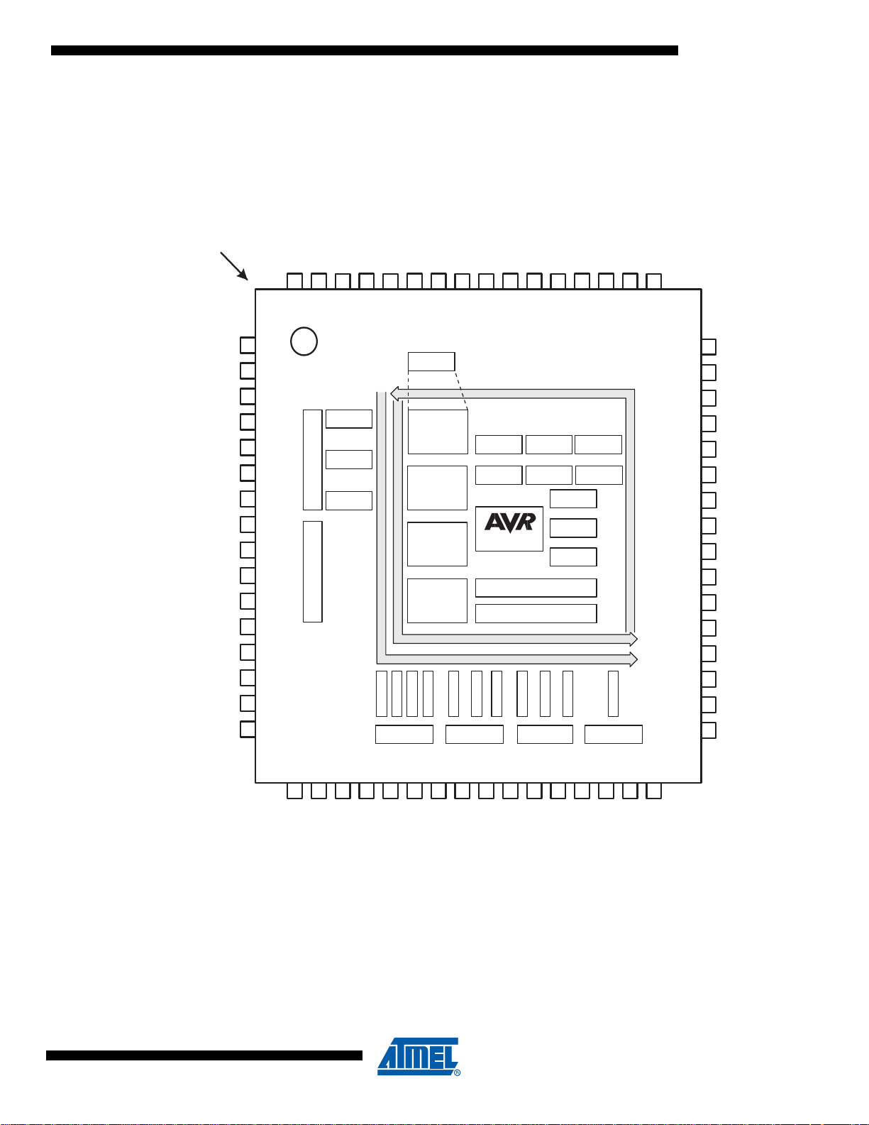
2. Pinout/ Block Diagram
INDEX CORNER
17
18
19
20
21
22
23
24
25
26
27
28
29
30
31
32
64
63
62
61
60
59
58
57
56
55
54
53
52
51
50
49
48
47
46
45
44
43
42
41
40
39
38
37
36
35
34
33
1
2
3
4
5
6
7
8
9
10
11
12
13
14
15
16
PF2
PF1
PF0
VCC
GND
PE7
PE6
PE5
PE4
PE3
PE2
PE1
PE0
VCC
GND
PD7
PA 3
PA 4
PA 5
PA 6
PA 7
PB0
PB1
PB2
PB3
PB4
PB5
PB6
PB7
GND
VCC
PC0
PC1
PC2
PC3
PC4
PC5
PC6
PC7
GND
VCC
PD0
PD1
PD2
PD3
PD4
PD5
PD6
PA 2
PA 1
PA 0
AVCC
GND
PR1
PR0
RESET/PDI
PDI
PF7
PF6
VCC
GND
PF5
PF4
PF3
FLASH
RAM
E2PROM
Interrupt Controller
OCD
ADC A
AC A0
AC A1
Por t
A
Por t
B
Event System ctrl
Por t R
Power
Control
Reset
Control
Watchdog
OSC/CLK
Control
BOD POR
RTC
EVENT ROUTING NETWORK
DATA BUS
DATA BU S
VREF
TEMP
Port C Port D Port E Port F
CPU
T/C0:1
USART0
SPI
TWI
T/C0
USART0
SPI
T/C0
USART0
T/C0
TWI
Figure 2-1. Block diagram and pinout
XMEGA D3
Notes: 1. For full details on pinout and alternate pin functions refer to ”Pinout and Pin Functions” on page 46.
2. The large center pad underneath the QFN/MLF package should be soldered to ground on the board to ensure good
mechanical stability.
8134I–AVR–12/10
3

3. Overview
XMEGA D3
The Atmel® AVR® XMEGA D3 is a family of low power, high performance and peripheral rich
CMOS 8/16-bit microcontrollers based on the AVR
powerful instructions in a single clock cycle, the XMEGA D3 achieves throughputs approaching
1 Million Instructions Per Second (MIPS) per MHz allowing the system designer to optimize
power consumption versus processing speed.
The AVR CPU combines a rich instruction set with 32 general purpose working registers. All the
32 registers are directly connected to the Arithmetic Logic Unit (ALU), allowing two independent
registers to be accessed in one single instruction, executed in one clock cycle. The resulting
architecture is more code efficient while achieving throughputs many times faster than conventional single-accumulator or CISC based microcontrollers.
The XMEGA D3 devices provide the following features: In-System Programmable Flash with
Read-While-Write capabilities, Internal EEPROM and SRAM, four-channel Event System, Programmable Multi-level Interrupt Controller, 50 general purpose I/O lines, 16-bit Real Time
Counter (RTC), five flexible 16-bit Timer/Counters with compare modes and PWM, three
USARTs, two Two-Wire Interface (TWIs), two Serial Peripheral Interfaces (SPIs), one 16-channel 12-bit ADC with optional differential input with programmable gain, two analog comparators
with window mode, programmable Watchdog Timer with separate Internal Oscillator, accurate
internal oscillators with PLL and prescaler and programmable Brown-Out Detection.
The Program and Debug Interface (PDI), a fast 2-pin interface for programming and debugging,
is available.
The XMEGA D3 devices have five software selectable power saving modes. The Idle mode
stops the CPU while allowing the SRAM, Event System, Interrupt Controller and all peripherals
to continue functioning. The Power-down mode saves the SRAM and register contents but stops
the oscillators, disabling all other functions until the next TWI or pin-change interrupt, or Reset.
In Power-save mode, the asynchronous Real Time Counter continues to run, allowing the application to maintain a timer base while the rest of the device is sleeping. In Standby mode, the
Crystal/Resonator Oscillator is kept running while the rest of the device is sleeping. This allows
very fast start-up from external crystal combined with low power consumption. In Extended
Standby mode, both the main Oscillator and the Asynchronous Timer continue to run. To further
reduce power consumption, the peripheral clock for each individual peripheral can optionally be
stopped in Active mode and Idle sleep mode.
®
enhanced RISC architecture. By execug
8134I–AVR–12/10
The device is manufactured using Atmel's high-density nonvolatile memory technology. The program Flash memory can be reprogrammed in-system through the PDI. A Bootloader running in
the device can use any interface to download the application program to the Flash memory. The
Bootloader software in the Boot Flash section will continue to run while the Application Flash
section is updated, providing true Read-While-Write operation. By combining an 8/16-bit RISC
CPU with In-System Self-Programmable Flash, the Atmel XMEGA D3 is a powerful microcontroller family that provides a highly flexible and cost effective solution for many embedded
applications.
The XMEGA D3 devices are supported with a full suite of program and system development
tools including: C compilers, macro assemblers, program debugger/simulators, programmers,
and evaluation kits.
4
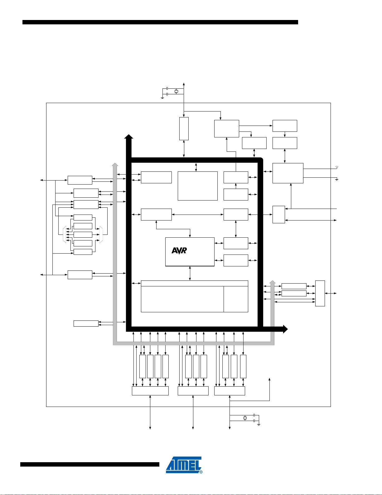
3.1 Block Diagram
Power
Supervisio n
POR/BOD &
RESET
PORT A (8)
PORT B (8)
BUS
Controller
SRAM
ADCA
ACA
OCD
PDI
CPU
PA[0..7]
PB[0..7]
Watchdog
Timer
Watchdog
Oscillator
Interrupt
Controller
DATA BUS
Prog/Debug
Controller
VCC
GND
PORT R (2)
XTAL1
XTAL2
PR[0..1]
Oscillato r
Circuits/
Clock
Generation
Oscillato r
Control
Real Time
Counter
Event System
Controller
PDI_DATA
RESET/
PDI_CLK
Sleep
Controller
Flash EEPROM
NVM Controller
IRCOM
PORT C (8)
PC[0..7]
TCC0:1
USARTC0:1
TWIC
SPIC
PD[0..7] PE[0..7]
PORT D (8)
TCD0:1
USARTD0:1
SPID
TCE0:1
USARTE0:1
Int. Refs .
AREFA
AREFB
Tempref
VCC/10
TOSC1
TOSC2
To Clock
Generator
TCF0
USARTF0
PORT F (8)
PF[0..7]
EVENT ROUTING NETWORK
DATA BUS
PORT E (8)
TWIE
Figure 3-1. XMEGA D3 Block Diagram
XMEGA D3
8134I–AVR–12/10
5

4. Resources
A comprehensive set of development tools, application notes and datasheets are available for
download on http://www.atmel.com/avr.
4.1 Recommended reading
•Atmel® AVR® XMEGATM D Manual
• XMEGA Application Notes
This device data sheet only contains part specific information and a short description of each
peripheral and module. The XMEGA D Manual describes the modules and peripherals in depth.
The XMEGA application notes contain example code and show applied use of the modules and
peripherals.
The XMEGA Manual and Application Notes are available from http://www.atmel.com/avr.
5. Disclaimer
For devices that are not available yet, typical values contained in this datasheet are based on
simulations and characterization of other AVR XMEGA microcontrollers manufactured on the
same process technology. Min. and Max values will be available after the device is
characterized.
XMEGA D3
8134I–AVR–12/10
6
6. AVR CPU
Flash
Program
Memory
Instruction
Decode
Program
Counter
OCD
32 x 8 General
Purpose
Registers
ALU
Multiplier/
DES
Instruction
Register
STATUS/
CONTROL
Peripheral
Module 1
Peripheral
Module 2
EEPROM PMICSRAM
DATA BUS
DATA BUS
6.1 Features
6.2 Overview
XMEGA D3
• 8/16-bit high performance AVR RISC Architecture
– 138 instructions
– Hardware multiplier
• 32x8-bit registers directly connected to the ALU
• Stack in RAM
• Stack Pointer accessible in I/O memory space
• Direct addressing of up to 16M bytes of program and data memory
• True 16/24-bit access to 16/24-bit I/O registers
• Support for 8-, 16- and 32-bit Arithmetic
• Configuration Change Protection of system critical features
The Atmel® AVR® XMEGA
TM
D3 uses the 8/16-bit AVR CPU. The main function of the AVR CPU
is to ensure correct program execution. The CPU must therefore be able to access memories,
perform calculations and control peripherals. Interrupt handling is described in a separate section. Figure 6-1 on page 7 shows the CPU block diagram.
Figure 6-1. CPU block diagram
8134I–AVR–12/10
The AVR uses a Harvard architecture - with separate memories and buses for program and
data. Instructions in the program memory are executed with a single level pipeline. While one
instruction is being executed, the next instruction is pre-fetched from the program memory.
7

This concept enables instructions to be executed in every clock cycle. The program memory is
In-System Re-programmable Flash memory.
6.3 Register File
The fast-access Register File contains 32 x 8-bit general purpose working registers with a single
clock cycle access time. This allows single-cycle Arithmetic Logic Unit (ALU) operation. In a typical ALU operation, two operands are output from the Register File, the operation is executed,
and the result is stored back in the Register File - in one clock cycle.
Six of the 32 registers can be used as three 16-bit indirect address register pointers for Data
Space addressing - enabling efficient address calculations. One of these address pointers can
also be used as an address pointer for look up tables in Flash program memory.
6.4 ALU - Arithmetic Logic Unit
The high performance Arithmetic Logic Unit (ALU) supports arithmetic and logic operations
between registers or between a constant and a register. Single register operations can also be
executed. Within a single clock cycle, arithmetic operations between general purpose registers
or between a register and an immediate are executed. After an arithmetic or logic operation, the
Status Register is updated to reflect information about the result of the operation.
XMEGA D3
6.5 Program Flow
The ALU operations are divided into three main categories – arithmetic, logical, and bit-functions. Both 8- and 16-bit arithmetic is supported, and the instruction set allows for easy
implementation of 32-bit arithmetic. The ALU also provides a powerful multiplier supporting both
signed and unsigned multiplication and fractional format.
When the device is powered on, the CPU starts to execute instructions from the lowest address
in the Flash Program Memory ‘0’. The Program Counter (PC) addresses the next instruction to
be fetched. After a reset, the PC is set to location ‘0’.
Program flow is provided by conditional and unconditional jump and call instructions, capable of
addressing the whole address space directly. Most AVR instructions use a 16-bit word format,
while a limited number uses a 32-bit format.
During interrupts and subroutine calls, the return address PC is stored on the Stack. The Stack
is effectively allocated in the general data SRAM, and consequently the Stack size is only limited
by the total SRAM size and the usage of the SRAM. After reset the Stack Pointer (SP) points to
the highest address in the internal SRAM. The SP is read/write accessible in the I/O memory
space, enabling easy implementation of multiple stacks or stack areas. The data SRAM can
easily be accessed through the five different addressing modes supported in the AVR CPU.
8134I–AVR–12/10
8

7. Memories
7.1 Features
7.2 Overview
XMEGA D3
• Flash Program Memory
– One linear address space
– In-System Programmable
– Self-Programming and Bootloader support
– Application Section for application code
– Application Table Section for application code or data storage
– Boot Section for application code or bootloader code
– Separate lock bits and protection for all sections
• Data Memory
– One linear address space
– Single cycle access from CPU
– SRAM
– EEPROM
Byte and page accessible
Optional memory mapping for direct load and store
– I/O Memory
Configuration and Status registers for all peripherals and modules
16 bit-accessible General Purpose Register for global variables or flags
• Production Signature Row Memory for factory programmed data
Device ID for each microcontroller device type
Serial number for each device
Oscillator calibration bytes
ADC and temperature sensor calibration data
• User Signature Row
One flash page in size
Can be read and written from software
Content is kept after chip erase
The AVR architecture has two main memory spaces, the Program Memory and the Data Memory. In addition, the XMEGA D3 features an EEPROM Memory for non-volatile data storage. All
three memory spaces are linear and require no paging. The available memory size configurations are shown in ”Ordering Information” on page 2. In addition each device has a Flash
memory signature row for calibration data, device identification, serial number etc.
Non-volatile memory spaces can be locked for further write or read/write operations. This prevents unrestricted access to the application software.
7.3 In-System Programmable Flash Program Memory
The XMEGA D3 devices contains On-chip In-System Programmable Flash memory for program
storage, see Figure 7-1 on page 10. Since all AVR instructions are 16- or 32-bits wide, each
Flash address location is 16 bits.
The Program Flash memory space is divided into Application and Boot sections. Both sections
have dedicated Lock Bits for setting restrictions on write or read/write operations. The Store Pro-
8134I–AVR–12/10
9

XMEGA D3
gram Memory (SPM) instruction must reside in the Boot Section when used to write to the Flash
memory.
A third section inside the Application section is referred to as the Application Table section which
has separate Lock bits for storage of write or read/write protection. The Application Table section can be used for storing non-volatile data or application software.
Figure 7-1. Flash Program Memory (Hexadecimal address)
Word Address
0
1EFFF / 16FFF / EFFF / 77FF
Application Section
(256K/192K/128K/64K)
...
1F000 / 17000 / F000 / 7800
1FFFF / 17FFF / FFFF / 7FFF
20000 / 18000 / 10000 / 8000
20FFF / 18FFF / 10FFF / 87FF
Application Table Section
(8K/8K/8K/4K)
Boot Section
(8K/8K/8K/4K)
The Application Table Section and Boot Section can also be used for general application
software.
8134I–AVR–12/10
10
XMEGA D3
7.4 Data Memory
The Data Memory consist of the I/O Memory, EEPROM and SRAM memories, all within one linear address space, see Figure 7-2 on page 11. To simplify development, the memory map for all
devices in the family is identical and with empty, reserved memory space for smaller devices.
Figure 7-2. Data Memory Map (Hexadecimal address)
Byte Address ATxmega192D3 Byte Address ATxmega128D3 Byte Address ATxmega64D3
0
FFF FFF FFF
1000
17FF 17FF 17FF
2000
5FFF 3FFF 2FFF
I/O Registers
(4KB)
EEPROM
(2K)
RESERVED RESERVED RESERVED
Internal SRAM
(16K)
1000
2000
0
I/O Registers
(4KB)
EEPROM
(2K)
Internal SRAM
(8K)
1000
2000
Byte Address ATxmega256D3
0
FFF
1000
1FFF
2000
5FFF
0
Internal SRAM
I/O Registers
Internal SRAM
I/O Registers
(4KB)
EEPROM
(2K)
(4K)
(4KB)
EEPROM
(4K)
(16K)
8134I–AVR–12/10
11

7.4.1 I/O Memory
All peripherals and modules are addressable through I/O memory locations in the data memory
space. All I/O memory locations can be accessed by the Load (LD/LDS/LDD) and Store
(ST/STS/STD) instructions, transferring data between the 32 general purpose registers in the
CPU and the I/O Memory.
The IN and OUT instructions can address I/O memory locations in the range 0x00 - 0x3F
directly.
I/O registers within the address range 0x00 - 0x1F are directly bit-accessible using the SBI and
CBI instructions. The value of single bits can be checked by using the SBIS and SBIC instructions on these registers.
The I/O memory address for all peripherals and modules in XMEGA D3 is shown in the ”Periph-
eral Module Address Map” on page 51.
7.4.2 SRAM Data Memory
The XMEGA D3 devices have internal SRAM memory for data storage.
7.4.3 EEPROM Data Memory
XMEGA D3
The XMEGA D3 devices have internal EEPROM memory for non-volatile data storage. It is
addressable either in a separate data space or it can be memory mapped into the normal data
memory space. The EEPROM memory supports both byte and page access.
8134I–AVR–12/10
12
7.5 Production Signature Row
The Production Signature Row is a separate memory section for factory programmed data. It
contains calibration data for functions such as oscillators and analog modules.
The production signature row also contains a device ID that identify each microcontroller device
type, and a serial number that is unique for each manufactured device. The device ID for the
available XMEGA D3 devices is shown in Table 7-1 on page 13. The serial number consist of
the production LOT number, wafer number, and wafer coordinates for the device.
The production signature row can not be written or erased, but it can be read from both application software and external programming.
Table 7-1. Device ID bytes for XMEGA D3 devices.
ATxmega64D3 4A 96 1E
ATxmega128D3 48 97 1E
ATxmega192D3 49 97 1E
XMEGA D3
Device Device ID bytes
Byte 2 Byte 1 Byte 0
7.6 User Signature Row
The User Signature Row is a separate memory section that is fully accessible (read and write)
from application software and external programming. The user signature row is one flash page
in size, and is meant for static user parameter storage, such as calibration data, custom serial
numbers or identification numbers, random number seeds etc. This section is not erased by
Chip Erase commands that erase the Flash, and requires a dedicated erase command. This
ensures parameter storage during multiple program/erase session and on-chip debug sessions.
ATxmega256D3 44 98 1E
8134I–AVR–12/10
13
XMEGA D3
7.7 Flash and EEPROM Page Size
The Flash Program Memory and EEPROM data memory is organized in pages. The pages are
word accessible for the Flash and byte accessible for the EEPROM.
Table 7-2 on page 14 shows the Flash Program Memory organization. Flash write and erase
operations are performed on one page at the time, while reading the Flash is done one byte at
the time. For Flash access the Z-pointer (Z[m:n]) is used for addressing. The most significant
bits in the address (FPAGE) gives the page number and the least significant address bits
(FWORD) gives the word in the page.
Table 7-2. Number of words and Pages in the Flash.
Devices Flash Page Size FWORD FPAGE Application Boot
Size (Bytes) (words) Size No of Pages Size No of Pages
ATxmega64D3 64K + 4K 128 Z[7:1] Z[16:8] 64K 256 4K 16
ATxmega128D3 128K + 8K 256 Z[8:1] Z[17:9] 128K 256 8K 16
ATxmega192D3 192K + 8K 256 Z[8:1] Z[18:9] 192K 384 8K 16
ATxmega256D3 256K + 8K 256 Z[8:1] Z[18:9] 256K 512 8K 16
Table 7-3 on page 14 shows EEPROM memory organization for the XMEGA D3 devices.
EEEPROM write and erase operations can be performed one page or one byte at the time, while
reading the EEPROM is done one byte at the time. For EEPROM access the NVM Address
Register (ADDR[m:n] is used for addressing. The most significant bits in the address (E2PAGE)
gives the page number and the least significant address bits (E2BYTE) gives the byte in the
page.
Table 7-3. Number of bytes and Pages in the EEPROM.
Devices EEPROM Page Size E2BYTE E2PAGE No of Pages
Size (Bytes) (Bytes)
ATxmega64D3 2K 32 ADDR[4:0] ADDR[10:5] 64
ATxmega128D3 2K 32 ADDR[4:0] ADDR[10:5] 64
ATxmega192D3 2K 32 ADDR[4:0] ADDR[10:5] 64
ATxmega256D3 4K 32 ADDR[4:0] ADDR[11:5] 128
8134I–AVR–12/10
14

8. Event System
8.1 Features
8.2 Overview
• Inter-peripheral communication and signalling with minimum latency
• CPU independent operation
• 4 Event Channels allows for up to 4 signals to be routed at the same time
• Events can be generated by
– Timer/Counters (TCxn)
– Real Time Counter (RTC)
– Analog to Digital Converters (ADC)
– Analog Comparators (AC)
– Ports (PORTx)
– System Clock (Clk
– Software (CPU)
SYS
)
• Events can be used by
– Timer/Counters (TCxn)
– Analog to Digital Converters (ADC)
– Ports (PORTx)
– IR Communication Module (IRCOM)
• The same event can be used by multiple peripherals for synchronized timing
• Advanced Features
– Manual Event Generation from software (CPU)
– Quadrature Decoding
– Digital Filtering
• Functions in Active and Idle mode
XMEGA D3
The Event System is a set of features for inter-peripheral communication. It enables the possibility for a change of state in one peripheral to automatically trigger actions in one or more
peripherals. What changes in a peripheral that will trigger actions in other peripherals are configurable by software. It is a simple, but powerful system as it allows for autonomous control of
peripherals without any use of interrupts or CPU resources.
The indication of a change in a peripheral is referred to as an event, and is usually the same as
the interrupt conditions for that peripheral. Events are passed between peripherals using a dedicated routing network called the Event Routing Network. Figure 8-1 on page 16 shows a basic
block diagram of the Event System with the Event Routing Network and the peripherals to which
it is connected. This highly flexible system can be used for simple routing of signals, pin functions or for sequencing of events.
The maximum latency is two CPU clock cycles from when an event is generated in one peripheral, until the actions are triggered in one or more other peripherals.
The Event System is functional in both Active and Idle modes.
8134I–AVR–12/10
15

Figure 8-1. Event system block diagram.
ADCx
Event Routing
Network
PORTx
CPU
ACx
RTC
T/CxnIRCOM
ClkSYS
XMEGA D3
The Event Routing Network can directly connect together ADCs, Analog Comparators (AC),
I/O ports (PORTx), the Real-time Counter (RTC), Timer/Counters (T/C) and the IR Communication Module (IRCOM). Events can also be generated from software (CPU).
All events from all peripherals are always routed into the Event Routing Network. This consist of
four multiplexers where each can be configured in software to select which event to be routed
into that event channel. All four event channels are connected to the peripherals that can use
events, and each of these peripherals can be configured to use events from one or more event
channels to automatically trigger a software selectable action.
8134I–AVR–12/10
16

9. System Clock and Clock options
9.1 Features
• Fast start-up time
• Safe run-time clock switching
• Internal Oscillators:
– 32 MHz run-time calibrated RC oscillator
– 2 MHz run-time calibrated RC oscillator
– 32.768 kHz calibrated RC oscillator
– 32 kHz Ultra Low Power (ULP) oscillator
• External clock options
– 0.4 - 16 MHz Crystal Oscillator
– 32.768 kHz Crystal Oscillator
– External clock
• PLL with internal and external clock options with 2 to 31x multiplication
• Clock Prescalers with 2 to 2048x division
• Fast peripheral clock running at 2 and 4 times the CPU clock speed
• Automatic Run-Time Calibration of internal oscillators
• Crystal Oscillator failure detection
9.2 Overview
XMEGA D3
XMEGA D3 has an advanced clock system, supporting a large number of clock sources. It incorporates both integrated oscillators, external crystal oscillators and resonators. A high frequency
Phase Locked Loop (PLL) and clock prescalers can be controlled from software to generate a
wide range of clock frequencies from the clock source input.
It is possible to switch between clock sources from software during run-time. After reset the
device will always start up running from the 2 Mhz internal oscillator.
A calibration feature is available, and can be used for automatic run-time calibration of the internal 2 MHz and 32 MHz oscillators. This reduce frequency drift over voltage and temperature.
A Crystal Oscillator Failure Monitor can be enabled to issue a Non-Maskable Interrupt and
switch to internal oscillator if the external oscillator fails. Figure 9-1 on page 18 shows the principal clock system in XMEGA D3.
8134I–AVR–12/10
17
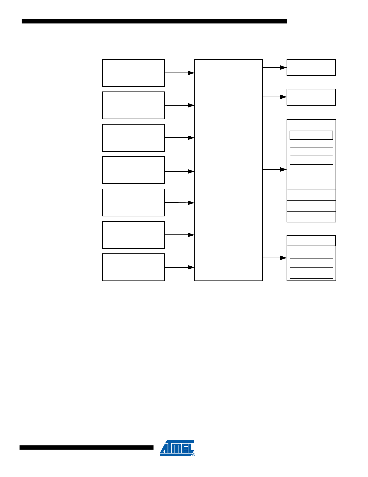
Figure 9-1. Clock system overview
32 MHz
Run-time Calibrated
Internal Oscillator
32 kHz ULP
Internal Oscillator
32.768 kHz
Calibrated Internal
Oscillator
32.768 KHz
Crystal Oscillator
0.4 - 16 MHz
Crystal Oscillator
2 MHz
Run-Time Calibrated
Internal Oscillator
External
Clock Input
CLOCK CONTROL
UNIT
with PLL and
Prescaler
WDT/BOD
clk
ULP
RTC
clk
RTC
EVSYS
PERIPHERALS
ADC
PORTS
...
clk
PER
INTERRUPT
RAM
NVM MEMORY
FLASH
EEPROM
CPU
clk
CPU
XMEGA D3
9.3 Clock Options
9.3.1 32 kHz Ultra Low Power Internal Oscillator
9.3.2 32.768 kHz Calibrated Internal Oscillator
Each clock source is briefly described in the following sub-sections.
The 32 kHz Ultra Low Power (ULP) Internal Oscillator is a very low power consumption clock
source. It is used for the Watchdog Timer, Brown-Out Detection and as an asynchronous clock
source for the Real Time Counter. This oscillator cannot be used as the system clock source,
and it cannot be directly controlled from software.
The 32.768 kHz Calibrated Internal Oscillator is a high accuracy clock source that can be used
as the system clock source or as an asynchronous clock source for the Real Time Counter. It is
calibrated during production to provide a default frequency which is close to its nominal
frequency.
8134I–AVR–12/10
18

9.3.3 32.768 kHz Crystal Oscillator
The 32.768 kHz Crystal Oscillator is a low power driver for an external watch crystal. It can be
used as system clock source or as asynchronous clock source for the Real Time Counter.
9.3.4 0.4 - 16 MHz Crystal Oscillator
The 0.4 - 16 MHz Crystal Oscillator is a driver intended for driving both external resonators and
crystals ranging from 400 kHz to 16 MHz.
9.3.5 2 MHz Run-time Calibrated Internal Oscillator
The 2 MHz Run-time Calibrated Internal Oscillator is a high frequency oscillator. It is calibrated
during production to provide a default frequency which is close to its nominal frequency. The
oscillator can use the 32.768 kHz Calibrated Internal Oscillator or the 32 kHz Crystal Oscillator
as a source for calibrating the frequency run-time to compensate for temperature and voltage
drift hereby optimizing the accuracy of the oscillator.
9.3.6 32 MHz Run-time Calibrated Internal Oscillator
The 32 MHz Run-time Calibrated Internal Oscillator is a high frequency oscillator. It is calibrated
during production to provide a default frequency which is close to its nominal frequency. The
oscillator can use the 32.768 kHz Calibrated Internal Oscillator or the 32 kHz Crystal Oscillator
as a source for calibrating the frequency run-time to compensate for temperature and voltage
drift hereby optimizing the accuracy of the oscillator.
XMEGA D3
9.3.7 External Clock input
The external clock input gives the possibility to connect a clock from an external source.
9.3.8 PLL with Multiplication factor 2 - 31x
The PLL provides the possibility of multiplying a frequency by any number from 2 to 31. In combination with the prescalers, this gives a wide range of output frequencies from all clock sources.
8134I–AVR–12/10
19

10. Power Management and Sleep Modes
10.1 Features
• 5 sleep modes
–Idle
– Power-down
–Power-save
–Standby
– Extended standby
• Power Reduction registers to disable clocks to unused peripherals
10.2 Overview
The XMEGA D3 provides various sleep modes tailored to reduce power consumption to a minimum. All sleep modes are available and can be entered from Active mode. In Active mode the
CPU is executing application code. The application code decides when and what sleep mode to
enter. Interrupts from enabled peripherals and all enabled reset sources can restore the microcontroller from sleep to Active mode.
In addition, Power Reduction registers provide a method to stop the clock to individual peripherals from software. When this is done, the current state of the peripheral is frozen and there is no
power consumption from that peripheral. This reduces the power consumption in Active mode
and Idle sleep mode.
XMEGA D3
10.3 Sleep Modes
10.3.1 Idle Mode
In Idle mode the CPU and Non-Volatile Memory are stopped, but all peripherals including the
Interrupt Controller and Event System are kept running. Interrupt requests from all enabled interrupts will wake the device.
10.3.2 Power-down Mode
In Power-down mode all system clock sources, and the asynchronous Real Time Counter (RTC)
clock source, are stopped. This allows operation of asynchronous modules only. The only interrupts that can wake up the MCU are the Two Wire Interface address match interrupts, and
asynchronous port interrupts, e.g pin change.
10.3.3 Power-save Mode
Power-save mode is identical to Power-down, with one exception: If the RTC is enabled, it will
keep running during sleep and the device can also wake up from RTC interrupts.
10.3.4 Standby Mode
Standby mode is identical to Power-down with the exception that all enabled system clock
sources are kept running, while the CPU, Peripheral and RTC clocks are stopped. This reduces
the wake-up time when external crystals or resonators are used.
8134I–AVR–12/10
20

10.3.5 Extended Standby Mode
Extended Standby mode is identical to Power-save mode with the exception that all enabled
system clock sources are kept running while the CPU and Peripheral clocks are stopped. This
reduces the wake-up time when external crystals or resonators are used.
XMEGA D3
8134I–AVR–12/10
21

11. System Control and Reset
11.1 Features
• Multiple reset sources for safe operation and device reset
– Power-On Reset
– External Reset
– Watchdog Reset
The Watchdog Timer runs from separate, dedicated oscillator
– Brown-Out Reset
Accurate, programmable Brown-Out levels
– PDI reset
– Software reset
• Asynchronous reset
– No running clock in the device is required for reset
• Reset status register
11.2 Resetting the AVR
During reset, all I/O registers are set to their initial values. The SRAM content is not reset. Application execution starts from the Reset Vector. The instruction placed at the Reset Vector should
be an Absolute Jump (JMP) instruction to the reset handling routine. By default the Reset Vector
address is the lowest Flash program memory address, ‘0’, but it is possible to move the Reset
Vector to the first address in the Boot Section.
XMEGA D3
The I/O ports of the AVR are immediately tri-stated when a reset source goes active.
The reset functionality is asynchronous, so no running clock is required to reset the device.
After the device is reset, the reset source can be determined by the application by reading the
Reset Status Register.
11.3 Reset Sources
11.3.1 Power-On Reset
The MCU is reset when the supply voltage VCC is below the Power-on Reset threshold voltage.
11.3.2 External Reset
The MCU is reset when a low level is present on the RESET pin.
11.3.3 Watchdog Reset
The MCU is reset when the Watchdog Timer period expires and the Watchdog Reset is enabled.
The Watchdog Timer runs from a dedicated oscillator independent of the System Clock. For
more details see ”WDT - Watchdog Timer” on page 23.
11.3.4 Brown-Out Reset
The MCU is reset when the supply voltage VCC is below the Brown-Out Reset threshold voltage
and the Brown-out Detector is enabled. The Brown-out threshold voltage is programmable.
11.3.5 PDI reset
8134I–AVR–12/10
The MCU can be reset through the Program and Debug Interface (PDI).
22

11.3.6 Software reset
The MCU can be reset by the CPU writing to a special I/O register through a timed sequence.
12. WDT - Watchdog Timer
12.1 Features
• 11 selectable timeout periods, from 8 ms to 8s.
• Two operation modes
– Standard mode
– Window mode
• Runs from the 1 kHz output of the 32 kHz Ultra Low Power oscillator
• Configuration lock to prevent unwanted changes
12.2 Overview
The XMEGA D3 has a Watchdog Timer (WDT). The WDT will run continuously when turned on
and if the Watchdog Timer is not reset within a software configurable time-out period, the microcontroller will be reset. The Watchdog Reset (WDR) instruction must be run by software to reset
the WDT, and prevent microcontroller reset.
XMEGA D3
The WDT has a Window mode. In this mode the WDR instruction must be run within a specified
period called a window. Application software can set the minimum and maximum limits for this
window. If the WDR instruction is not executed inside the window limits, the microcontroller will
be reset.
A protection mechanism using a timed write sequence is implemented in order to prevent
unwanted enabling, disabling or change of WDT settings.
For maximum safety, the WDT also has an Always-on mode. This mode is enabled by programming a fuse. In Always-on mode, application software can not disable the WDT.
8134I–AVR–12/10
23

13. PMIC - Programmable Multi-level Interrupt Controller
13.1 Features
• Separate interrupt vector for each interrupt
• Short, predictable interrupt response time
• Programmable Multi-level Interrupt Controller
– 3 programmable interrupt levels
– Selectable priority scheme within low level interrupts (round-robin or fixed)
– Non-Maskable Interrupts (NMI)
• Interrupt vectors can be moved to the start of the Boot Section
13.2 Overview
XMEGA D3 has a Programmable Multi-level Interrupt Controller (PMIC). All peripherals can
define three different priority levels for interrupts; high, medium or low. Medium level interrupts
may interrupt low level interrupt service routines. High level interrupts may interrupt both lowand medium level interrupt service routines. Low level interrupts have an optional round robin
scheme to make sure all interrupts are serviced within a certain amount of time.
The built in oscillator failure detection mechanism can issue a Non-Maskable Interrupt (NMI).
XMEGA D3
13.3 Interrupt vectors
When an interrupt is serviced, the program counter will jump to the interrupt vector address. The
interrupt vector is the sum of the peripheral’s base interrupt address and the offset address for
specific interrupts in each peripheral. The base addresses for the XMEGA D3 devices are
shown in Table 13-1. Offset addresses for each interrupt available in the peripheral are
described for each peripheral in the XMEGA A manual. For peripherals or modules that have
only one interrupt, the interrupt vector is shown in Table 13-1. The program address is the word
address.
Table 13-1. Reset and Interrupt Vectors
Program Address
(Base Address) Source Interrupt Description
0x000 RESET
0x002 OSCF_INT_vect Crystal Oscillator Failure Interrupt vector (NMI)
0x004 PORTC_INT_base Port C Interrupt base
0x008 PORTR_INT_base Port R Interrupt base
0x014 RTC_INT_base Real Time Counter Interrupt base
0x018 TWIC_INT_base Two-Wire Interface on Port C Interrupt base
0x01C TCC0_INT_base Timer/Counter 0 on port C Interrupt base
0x028 TCC1_INT_base Timer/Counter 1 on port C Interrupt base
0x030 SPIC_INT_vect SPI on port C Interrupt vector
0x032 USARTC0_INT_base USART 0 on port C Interrupt base
0x040 NVM_INT_base Non-Volatile Memory Interrupt base
0x044 PORTB_INT_base Port B Interrupt base
0x056 PORTE_INT_base Port E INT base
8134I–AVR–12/10
24

Table 13-1. Reset and Interrupt Vectors (Continued)
Program Address
(Base Address) Source Interrupt Description
0x05A TWIE_INT_base Two-Wire Interface on Port E Interrupt base
0x05E TCE0_INT_base Timer/Counter 0 on port E Interrupt base
0x074 USARTE0_INT_base USART 0 on port E Interrupt base
0x080 PORTD_INT_base Port D Interrupt base
0x084 PORTA_INT_base Port A Interrupt base
0x088 ACA_INT_base Analog Comparator on Port A Interrupt base
0x08E ADCA_INT_base Analog to Digital Converter on Port A Interrupt base
0x09A TCD0_INT_base Timer/Counter 0 on port D Interrupt base
0x0AE SPID_INT_vector SPI D Interrupt vector
0x0B0 USARTD0_INT_base USART 0 on port D Interrupt base
0x0D0 PORTF_INT_base Port F Interrupt base
0x0D8 TCF0_INT_base Timer/Counter 0 on port F Interrupt base
XMEGA D3
8134I–AVR–12/10
25

14. I/O Ports
14.1 Features
14.2 Overview
XMEGA D3
• Selectable input and output configuration for each pin individually
• Flexible pin configuration through dedicated Pin Configuration Register
• Synchronous and/or asynchronous input sensing with port interrupts and events
– Sense both edges
– Sense rising edges
– Sense falling edges
– Sense low level
• Asynchronous wake-up from all input sensing configurations
• Two port interrupts with flexible pin masking
• Highly configurable output driver and pull settings:
– Totem-pole
– Pull-up/-down
– Wired-AND
– Wired-OR
– Bus-keeper
– Inverted I/O
• Optional Slew rate control
• Configuration of multiple pins in a single operation
• Read-Modify-Write (RMW) support
• Toggle/clear/set registers for Output and Direction registers
• Clock output on port pin
• Event Channel 0 output on port pin 7
• Mapping of port registers (virtual ports) into bit accessible I/O memory space
The XMEGA D3 devices have flexible General Purpose I/O Ports. A port consists of up to 8 pins,
ranging from pin 0 to pin 7. The ports implement several functions, including synchronous/asynchronous input sensing, pin change interrupts and configurable output settings. All functions are
individual per pin, but several pins may be configured in a single operation.
14.3 I/O configuration
All port pins (Pn) have programmable output configuration. In addition, all port pins have an
inverted I/O function. For an input, this means inverting the signal between the port pin and the
pin register. For an output, this means inverting the output signal between the port register and
the port pin. The inverted I/O function can be used also when the pin is used for alternate
functions.
8134I–AVR–12/10
26
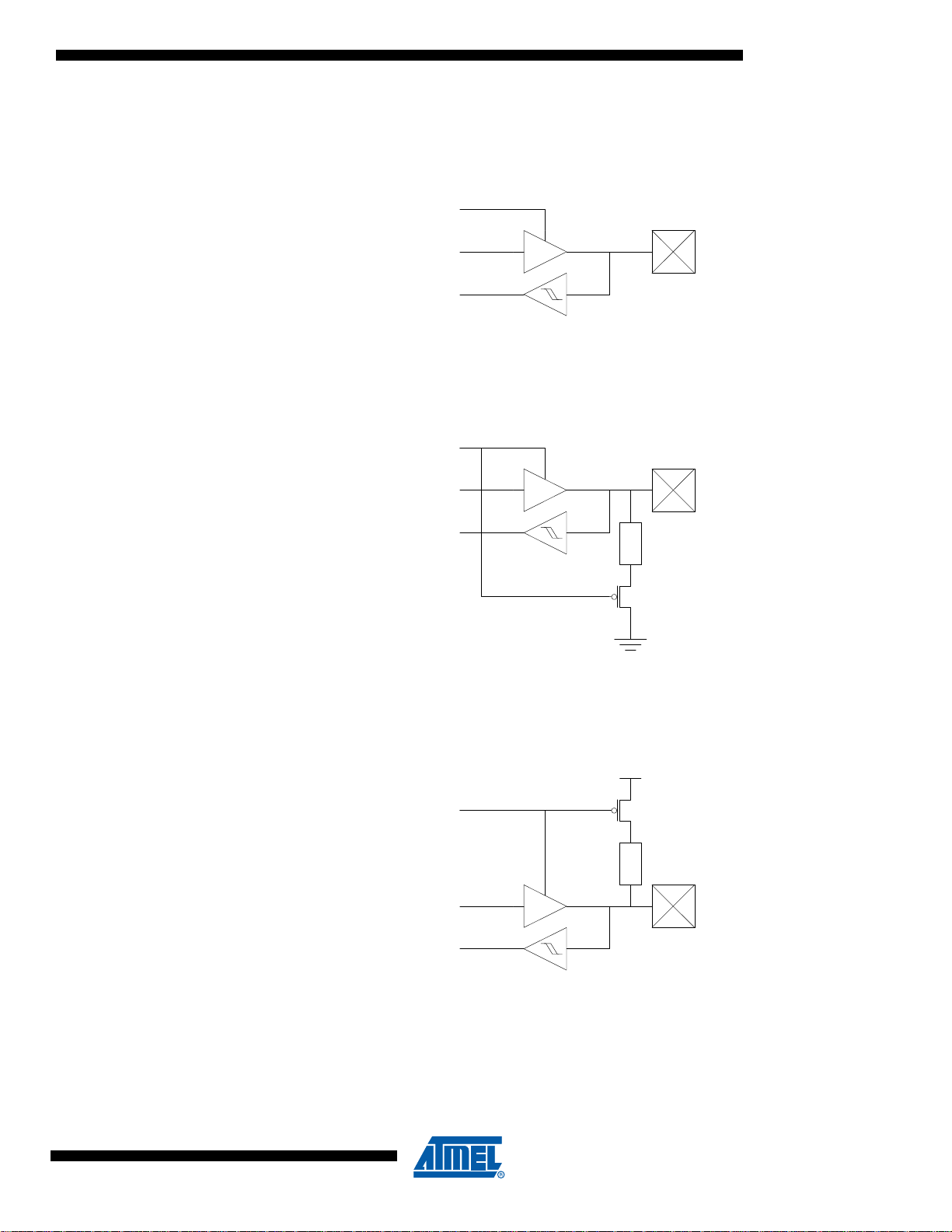
14.3.1 Push-pull
INn
OUTn
DIRn
Pn
INn
OUTn
DIRn
Pn
INn
OUTn
DIRn
Pn
14.3.2 Pull-down
XMEGA D3
Figure 14-1. I/O configuration - Totem-pole
Figure 14-2. I/O configuration - Totem-pole with pull-down (on input)
14.3.3 Pull-up
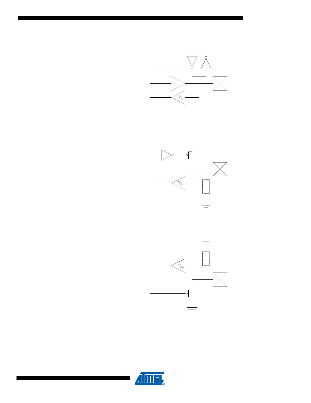
14.3.4 Bus-keeper
8134I–AVR–12/10
Figure 14-3. I/O configuration - Totem-pole with pull-up (on input)
The bus-keeper’s weak output produces the same logical level as the last output level. It acts as
a pull-up if the last level was ‘1’, and pull-down if the last level was ‘0’.
27
14.3.5 Others
INn
OUTn
DIRn
Pn
INn
OUTn
Pn
INn
OUTn
Pn
XMEGA D3
Figure 14-4. I/O configuration - Totem-pole with bus-keeper
Figure 14-5. Output configuration - Wired-OR with optional pull-down
8134I–AVR–12/10
Figure 14-6. I/O configuration - Wired-AND with optional pull-up
28

14.4 Input sensing
IN V ERTED I/O
Interrupt
Control
IR E Q
Event
Pn
D
Q
R
D
Q
R
Synchronizer
INn
EDGE
DETECT
Asynchronous sen sing
Synchronous sen sing
EDGE
DETECT
XMEGA D3
• Sense both edges
• Sense rising edges
• Sense falling edges
• Sense low level
Input sensing is synchronous or asynchronous depending on the enabled clock for the ports,
and the configuration is shown in Figure 14-7 on page 29.
Figure 14-7. Input sensing system overview
When a pin is configured with inverted I/O, the pin value is inverted before the input sensing.
14.5 Port Interrupt
Each port has two interrupts with separate priority and interrupt vector. All pins on the port can
be individually selected as source for each of the interrupts. The interrupts are then triggered
according to the input sense configuration for each pin configured as source for the interrupt.
14.6 Alternate Port Functions
In addition to the input/output functions on all port pins, most pins have alternate functions. This
means that other modules or peripherals connected to the port can use the port pins for their
functions, such as communication or pulse-width modulation. ”Pinout and Pin Functions” on
page 46 shows which modules on peripherals that enable alternate functions on a pin, and
which alternate functions that is available on a pin.
8134I–AVR–12/10
29

15. T/C - 16-bits Timer/Counter with PWM
15.1 Features
• Five 16-bit Timer/Counters
– Four Timer/Counters of type 0
– One Timer/Counters of type 1
• Four Compare or Capture (CC) Channels in Timer/Counter 0
• Two Compare or Capture (CC) Channels in Timer/Counter 1
• Double Buffered Timer Period Setting
• Double Buffered Compare or Capture Channels
• Waveform Generation:
– Single Slope Pulse Width Modulation
– Dual Slope Pulse Width Modulation
– Frequency Generation
• Input Capture:
– Input Capture with Noise Cancelling
– Frequency capture
– Pulse width capture
– 32-bit input capture
• Event Counter with Direction Control
• Timer Overflow and Timer Error Interrupts and Events
• One Compare Match or Capture Interrupt and Event per CC Channel
• Hi-Resolution Extension (Hi-Res)
• Advanced Waveform Extension (AWEX)
XMEGA D3
15.2 Overview
XMEGA D3 has five Timer/Counters, four Timer/Counter 0 and one Timer/Counter 1. The difference between them is that Timer/Counter 0 has four Compare/Capture channels, while
Timer/Counter 1 has two Compare/Capture channels.
The Timer/Counters (T/C) are 16-bit and can count any clock, event or external input in the
microcontroller. A programmable prescaler is available to get a useful T/C resolution. Updates of
Timer and Compare registers are double buffered to ensure glitch free operation. Single slope
PWM, dual slope PWM and frequency generation waveforms can be generated using the Compare Channels.
Through the Event System, any input pin or event in the microcontroller can be used to trigger
input capture, hence no dedicated pins are required for this. The input capture has a noise canceller to avoid incorrect capture of the T/C, and can be used to do frequency and pulse width
measurements.
A wide range of interrupt or event sources are available, including T/C Overflow, Compare
match and Capture for each Compare/Capture channel in the T/C.
PORTC has one Timer/Counter 0 and one Timer/Counter1. PORTD, PORTE and PORTF each
have one Timer/Counter 0. Notation of these are TCC0 (Time/Counter C0), TCC1, TCD0, TCE0,
and TCF0, respectively.
8134I–AVR–12/10
30
 Loading...