

ATMEL ATV750BL-25SC, ATV750BL-25PI, ATV750BL-25PC, ATV750BL-25JI, ATV750BL-25JC Datasheet
...
1
Features
•
Advanced, High-Speed Programmable Logic Device-Superset of 22V10
– Improved Performance - 7.5 ns tPD, 95 MHz External Operation
– Enhanced Logic Flexibility
– Backward Compatible with ATV750/L Software and Hardware
•
New Flip-Flop Features
– D- or T-Type
– Product Term or Direct Input Pin Clocking
•
High-Speed Erasable Programmable Logic Devices
– 7.5 ns Maximum Pin-to-Pin Delay
•
Highest Density Programmable Logic Available in a 24-Pin Package
•
Increased Logic Flexibility
– 42 Array Inputs, 20 Sum Terms and 20 Flip-Flops
•
Enhanced Output Logic Flexibility
– All 20 Flip-Flops Feed Back Internally
– 10 Flip-Flops are Also Available as Outputs
•
Full Military, Commercial and Industrial Temperature Ranges
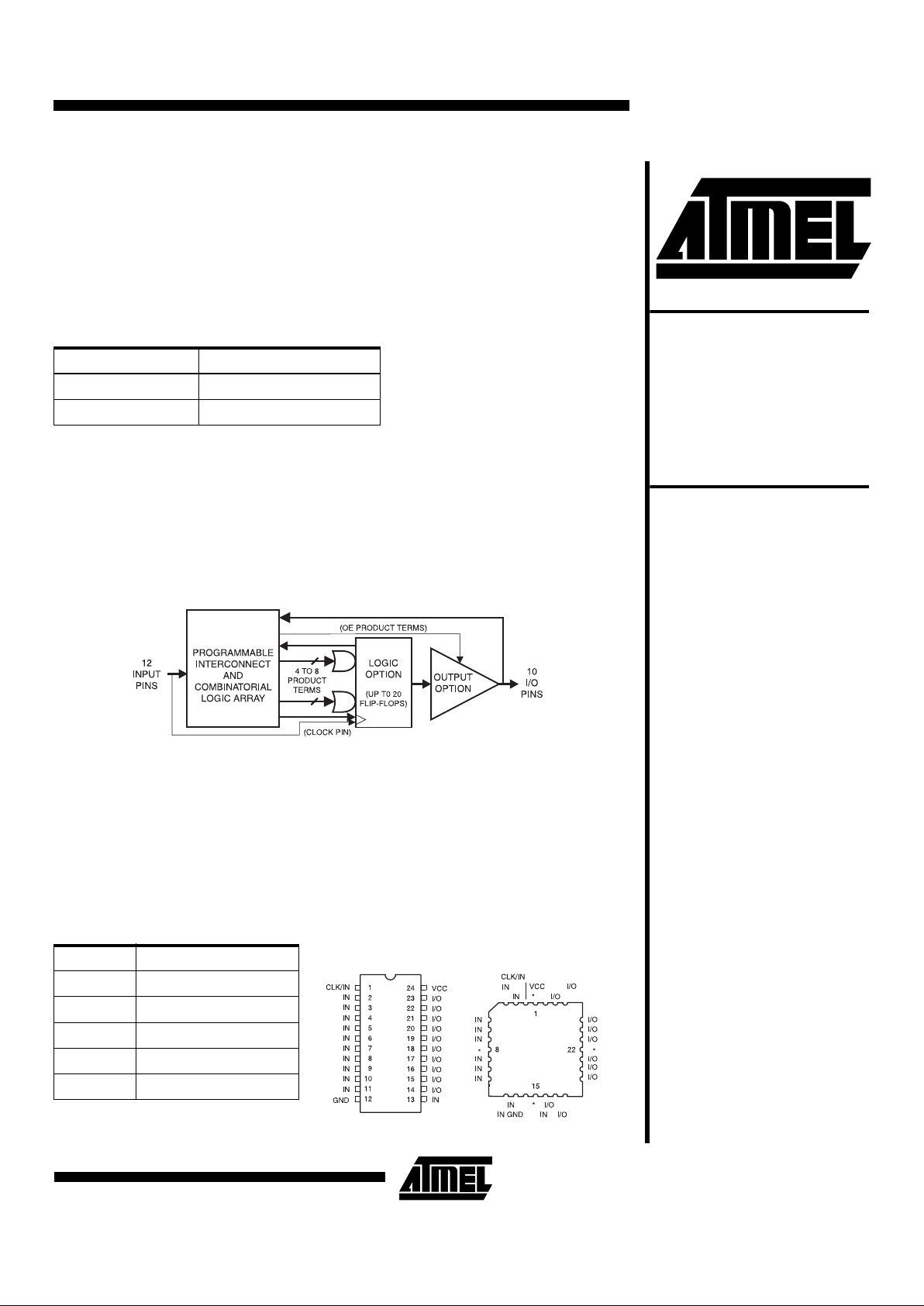
Logic Diagram
Description
The ATV750Bs are twice as powerful as most othe r 24-pin programmable logic
devices. Increased product terms, sum terms, flip-flops and output logic configurations
translate into mo re usable g ates. High-sp eed logic and unifor m, predict able delays
guarantee fast in-system performance.
Device ICC, Stand-By
ATV750B 125 mA
ATV750BL 15 mA
Rev. 0301D–05/98
High-Speed
UV-Erasable
Programmable
Logic Device
ATV750B
Pin Configurations
Pin Name Function
CLK Clock
IN Logic Inputs
I/O Bidirectional Buffers
* No Internal Connection
V
CC
+5V Supply
DIP/SOIC PLCC/LCC
T op View
(continued)
ATV750B
2
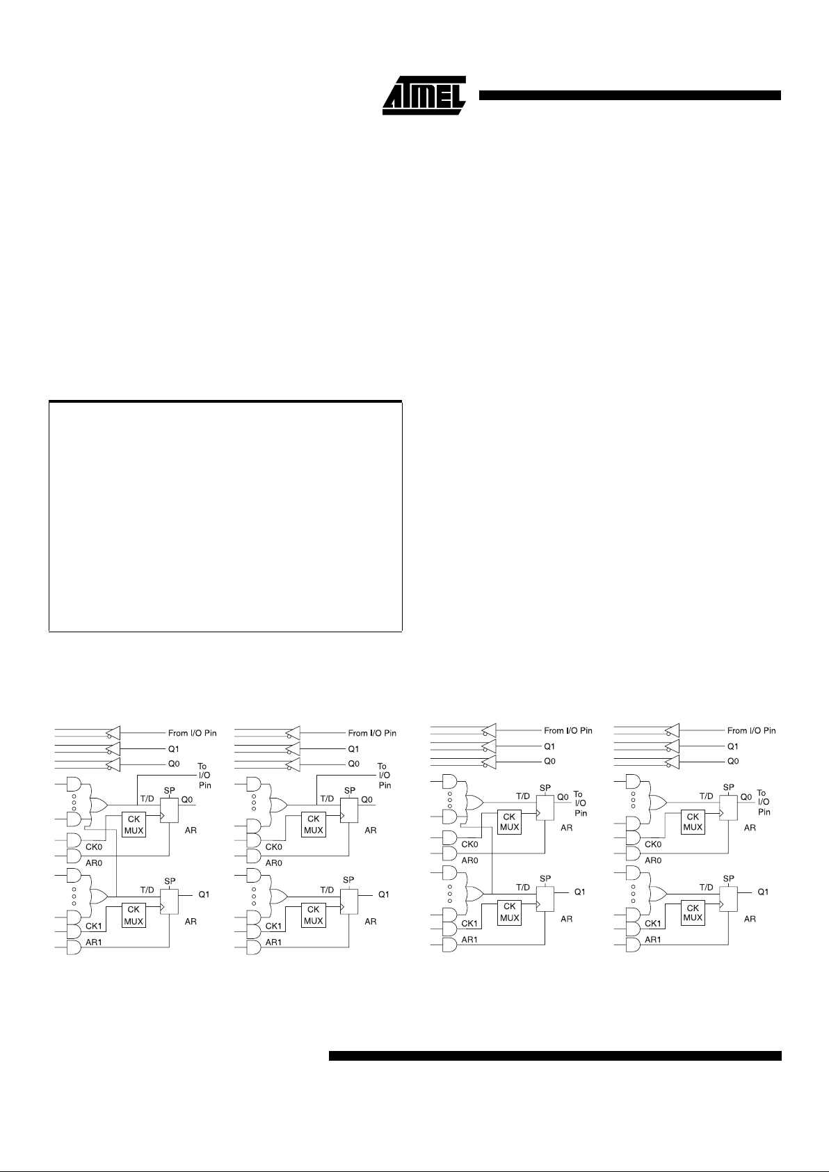
Each of the ATV750B’s 22 logic pi ns can be used as an
input. Ten of these can be used as inputs, outputs or bidirectional I/O pins. Each flip-flop is individually configurable as either D- or T-type. Each fl ip-flop output is fed
back into the array independently. This allows burying of all
the sum terms and flip-flops.
There are 171 total product terms avai lable. A va riable format is used to assign between four to eight product terms
per sum term. There are two sum terms per outpu t, providing added flexibility. Much more logic can be replaced by
this device than by any other 24-pin PLD. Wi th 20 sum
terms and flip-flops, complex state machines are easily
implemented with logic to spare.
Product terms provide individual clocks and asynchronous
resets for each flip-flop. Each flip-flop may also be individually configured to have direct input pin controlled clocking.
Each output has i ts o wn ena ble p roduct term. One produc t
term provides a com mon synchronous preset for a ll flipflops. Registe r prel oad fun ctions a re prov ided t o simp lify
testing. All registers automatically reset upon power up.
The ATV750BL is a low power device with speeds as fast
as 15 ns. The ATV750BL pro vides the optimu m low power
PLD solution, with full CMOS output levels. This device significantly reduces total system power, thereby allowing battery-powered operation.
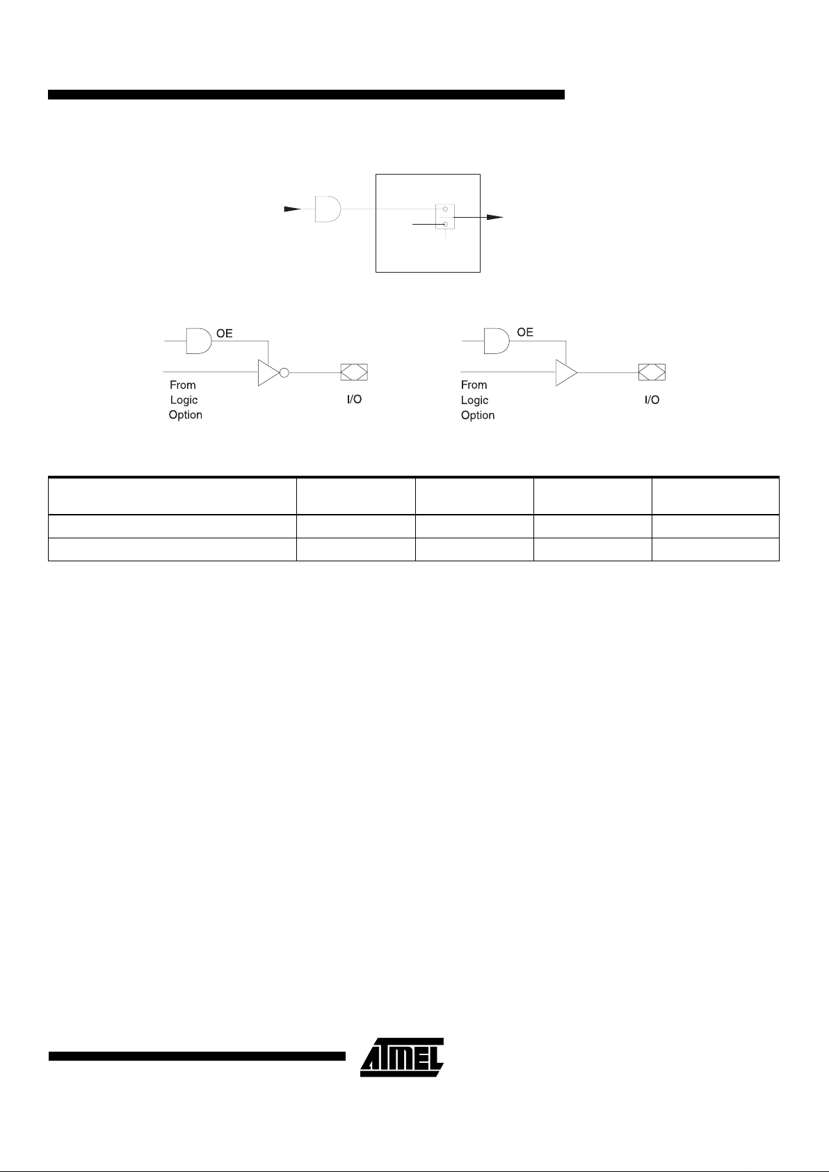
Logic Options
Combinatorial Output Registered Output
Abosute Maximum Rating*
Temperature Under Bias................................ -55°C to +125°C
*NOTICE: Stresses beyond those listed under “Absolute
Maximum Ratings” may cause permanent damage to the dev ice. Th is is a s tress rating only an d
functional oper ati on of the devi ce at t hes e o r any
other conditions beyond those indicated in the
operational sections of this specification is not
implied. Exposure to absolute maximum rating
conditions f or e xtended periods ma y af fect dev ice
reliability .
Note: 1. Minimum voltage is -0.6V DC which may under-
shoot to -2.0V for pulses of less than 20 ns.Maximum output pin v ol tage is V
CC
+ 0.75V DC which
may o versh oot to +7.0V f or pulse s of less than 20
ns.
Storage Temperature..................................... -65°C to +150°C
Voltage on Any Pin with
Respect to Ground .........................................-2.0V to +7.0V
(1)
Voltage on Input Pins
with Respect to Ground
During Programming.....................................-2.0V to +14.0V
(1)
Programming Voltage with
Respect to Ground .......................................-2.0V to +14.0V
(1)
Integrated UV Erase Dose ..............................7258 W•sec/cm
2
Combined T erms Separate Terms
Combined T erms Separate Terms
ATV750B
3
Clock MUX
Output Options
Note: 1. See ordering information for valid speed and temperature combination.
DC and AC Operating Conditions
(1)
Commercial
-7, -10, -15
Commercial
-25 Industrial Military
Operating Temperature (Case) 0°C - 70°C 0°C - 70°C -40°C - 85°C -55°C - 125°C
V
CC
Power Supply 5V ± 5% 5V ± 10% 5V ± 10% 5V ± 10%
SELECT
LOGIC
TO
CELL
CLOCK
PRODUCT
TERM
CLK
CKi
CKMUX
PIN
ATV750B
4
Notes: 1. Not more than one output at a time should be shorted. Duration of short circuit test should not exceed 30 sec.
Input Test Waveforms and
Measurement Levels
tR, tF < 3 ns (10% to 90%)
Output Test Load
DC Characteristics
Symbol Parameter Condition Min Typ Max Units
I
LI
Input Load Current VIN = -0.1V to VCC + 1V 10 µA
I
LO
Output Leakage
Current
V
OUT
= -0.1V to VCC + 0.1V 10 µA
I
CC
Po wer Supply
Current, Standby
V
CC
= MAX,
V
IN
= MAX,
Outputs Open
B-7, -10
Com. 125 180 mA
Ind.,Mil. 125 190 mA
B-15, -25
Com. 125 180 mA
Ind.,Mil. 125 190 mA
BL-15
Com. 15 30 mA
Ind.,Mil. 15 30 mA
I
OS
(1)
Output Short
Circuit Current
V
OUT
= 0.5V -120 mA
V
IL
Input Low Voltage 4.5 ≤ VCC ≤ 5.5V -0.6 0.8 V
V
IH
Input High Voltage 2.0 V
CC
+ 0.75 V
V
OL
Output Low
Voltage
VIN = VIH or VIL,
V
CC
= MIN
I
OL
= 16 mA Com.,Ind. 0.5 V
I
OL
= 12 mA Mil. 0.5 V
I
OL
= 24 mA Com. 0.8 V
V
OH
Output High
Voltage
VIN = VIH or VIL,
V
CC
= MIN
IOH = -100 µAV
CC
- 0.3 V
I
OH
= -4.0 mA 2.4 V
ATV750B
5
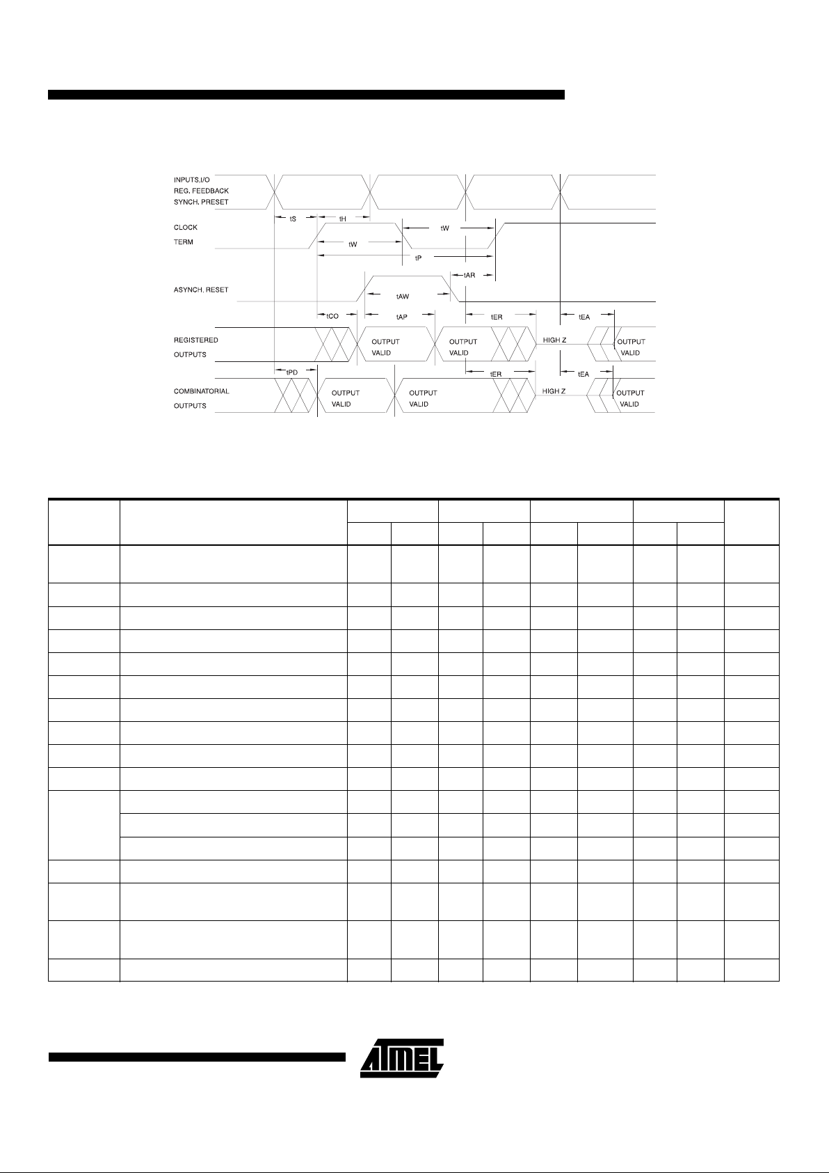
AC Wa veforms, Product Term Clock
(1)
Note: 1. Timing measurement reference is 1.5V. Input AC driving levels are 0.0V and 3.0V, unless otherwise specified.
Note: 1. See ordering information for valid par t numbers.
AC Characteristics, Product Term Clock
(1)
Symbol Parameter
-7 -10 B/BL-15 B/BL-25
UnitsMin Max Min Max Min Max Min Max
t
PD
Input or Feedback to
Non-Registered Outpu t
7.5 10 15 25 ns
t
EA
Input to Output Enable 7.5 10 15 25 ns
t
ER
Input to Output Disable 7.5 10 15 25 ns
t
CO
Clock to Output 3 7.5 4 10 5 12 6 20 ns
t
CF
Clock to Feedback 1 5 4 7.5 5 9 5 10 ns
t
S
Input Setup Time 3 4 8/12 14 ns
t
SF
Feedback Setup Time 3 4 7 7 ns
t
H
Hold Time 1 2 5/7 5/7 ns
t
P
Clock Period 7 11 14 17 ns
t
W
Clock Width 3.5 5.5 7 8.5 ns
F
MAX
External Feedback 1/(tS+tCO) 95 71 50/41 29 MHz
Internal Feedback 1/(t
SF+tCF
) 125 86 62 58 MHz
No Feedback 1/(t
P
) 142 90 71 58 MHz
t
AW
Asynchronous Reset Width 5 10 15 20 ns
t
AR
Asynchronous Reset
Recovery Time
31015 20ns
t
AP
Asynchronous Reset to
Registered Output Reset
812 1525ns
t
SP
Setup Time, Synchronous Preset 4 7 8 15 ns

ATV750B
6
A C Waveforms, Input Pin Clock
(1)
Notes: 1. Timing measurement reference is 1.5V. Input AC driving levels are 0.0V and 3.0V, unless otherwise specified.
AC Characteristics, Input Pin Clock
Symbol Parameter
-7 -10
B/BL
-15
B/BL
-25
UnitsMin Max Min Max Min Max Min Max
t
PD
Input or Feedback to
Non-Registered Output
7.5 10 15 25 ns
t
EA
Input to Output Enable 7.5 10 15 25 ns
t
ER
Input to Output Disable 7.5 10 15 25 ns
t
COS
Clock to Output 0 6.5 0 7 0 6.5 0 12 ns
t
CFS
Clock to Feedback 0 3.5 0 5 0 5.5 0 7 ns
t
SS
Input Setup Time 4 5 8/12.5 9/15 ns
t
SFS
Feedback Setup Time 4 5 7 9 ns
t
HS
Hold Time 0 0 0 0 ns
t
PS
Clock Period 7 10 12 16 ns
t
WS
Clock Width 3.5 5 6 8 ns
F
MAXS
External Feedback 1/(tSS+t
COS
) 95 83 69/52 48/37 MHz
Internal Feedback 1/(t
SFS+tCFS
) 133 100 80 62 MHz
No Feedback 1/(tPS) 142 100 83 62 MHz
t
AW
Asynchronous Reset Width 5 10 15 20 ns
t
ARS
Asynchronous Reset
Recovery Time
510 15 25 ns
t
AP
Asynchronous Reset to
Registered Output Reset
810 15 25ns
t
SPS
Setup Time, Synchronous
Preset
5 5/9 11 15 ns

ATV750B
7
Functional Logic Diagram ATV750B, Upper Half

ATV750B
8
Functional Logic Diagram ATV750B, Lower Half

ATV750B
9
Preload of Registered Outputs
The ATV750B’s registers are provided with circuitry to
allow loading of eac h regi ster async hro nously with eit her a
high or a low. This feature will simplify testing since any
state can be forced into the registers to control test
sequencing. A V
IH
level on the I/O pin will force the register
high; a V
IL
will force it low, inde pen den t of the output polar-
ity. The PRELOAD state is entered by placing a 10.25V to
10.75V signal on pin 8 on DIPs, and lead 10 on SMDs.
When the clock term is pulsed high, the data on the I/O
pins is placed into the register chosen by the Select Pin.
Power Up Reset
The registers in the ATV750Bs are designed to reset during
power up. At a point delayed slightly from V
CC
crossing
V
RST
, all registers wil l be rese t to the low state. Th e outpu t
state will depend on the polarity of the output buffer.
This feature is critical for state machine initialization. How-
ever, due to the asynchronous nature of reset and the
uncertainty of h ow V
CC
actually rises in the sys tem, the fo l-
lowing conditions are required:
1. The V
CC
rise must be monotonic,
2. After reset occurs, all input and feedback setup
times must be met before driving the clock terms or
pin high, and
3. The clock pin, or signals from which clock terms are
derived, must remain stable during t
PR
.
Level forced on registered
output pin during PRELOAD cycle Select Pin State Register #0 State after cycle Register #1 State after cycle
V
IH
Low High X
V
IL
Low Low X
V
IH
High X High
V
IL
High X Low
Parameter Description Typ Max Units
t
PR
Power-Up Reset Time 600 1000 ns
V
RST
Power-Up Reset Voltage 3.8 4.5 V
Pin Capacitance
f = 1 MHz, T = 25°C
(1)
T yp Max Units Conditions
C
IN
58 pFV
IN
= 0V
C
OUT
68 pFV
OUT
= 0V

ATV750B
10
Using the ATV750B’s Many Advanced
Features
The ATV750B’s advanced flexibility packs more usable
gates into 24-pins than any other logic device. The
ATV750Bs start with the popular 22V10 ar chitecture, an d
add several enhanced features:
•
Selectable D- and T-Type Registers -
Each ATV7 50B flip-flop can be individually configured as
either D- or T-type. Using the T-type configuration, JK
and SR flip-flops ar e also easily created. These options
allow mo re efficient product term usag e.
•
Selectable Asynchronous Clocks -
Each of the ATV 750B’s flip-flops may be clocked by its
own clock product term or directly from Pin 1 (SMD Lead
2). This removes the constraint that all registers must
use the same clock. Buried state machines, counters
and registers can a ll coexist in one device while r unning
on separate clocks. Individual flip-flop clock source
selection further allows mixing higher performance pin
clocking and flexible product term clocking within one
design.
•
A Full Bank of Ten More Registers -
The ATV750B p rovid es two f li p-f lo ps pe r output logic cell
for a total of 20. Each register has its own sum term, its
own reset term and its own clock term.
•
Independent I/O Pin and Feedback Paths -
Each I/O pin on the A TV750B has a dedicated input path.
Each of the 20 regi sters h as its own feedback ter ms int o
the array as well. This feature, combined with individual
product terms for each I/O’s output enable, facilitates
true bi-directional I/O design.
Programming Software Support
As with all other A tmel PLDs, severa l third party devel opment software products support the ATV75 0Bs. Several
third party programmers s upport the ATV750B as well.
Additionally, the ATV 750B m ay be p rogramm ed to pe rform
the ATV750/L’s functional subset (no T-type flip-flops or pin
clocking) using the ATV750/L JEDEC file. In this case, the
ATV750B becomes a direct repl ac eme nt or sp eed upgr ad e
for the ATV750/L. The ATV750/L programming algorithm is
different from the ATV750B algorithm. Choose the appropriate devic e in your p rogramm er menu to ensure proper
programming. Please refer to the
Programmable Log ic
Development Tools
section for a complete PLD software
and programmer listing.
Synchronous Preset and
Asynchronous Reset
One synchronous pres et li ne is pr ov id ed for all 20 regi sters
in the ATV750B. The appropriate input signals to cause the
internal clocks to go to a high state must be received during
a synchronous preset. Appropriate setup and hold times
must be met, as shown in the switching waveform diagram.
An individual asynchronous reset line is provided for each
of the 20 flip-flops. Both master and slave halves of the flipflops are reset when the input signals received force the
internal resets high.
Security Fuse Usage
A single fuse is provided to prevent unauthoriz ed copying
of the ATV750B fuse pa tterns. Once the securit y fuse is
programmed, all fuses will appe ar prog ramme d during verify.
The security fuse should be programmed last, as its effect
is immediate.
Erasure Characteristics
The entire memory array of an AT V750B is erased after
exposure to ultraviolet light at a wavel ength of 2537 Å.
Complete erasure is assured after a minimum of 20 minutes exposure using 1 2,000 µW/cm
2
intensity lamps
spaced one inch away from the chip. Minimum erase time
for lamps at other intensity ratings can be calc ulated from
the minimum inte grated erasur e dose of 1 5 W
•
sec/cm2. To
prevent unintentional erasure, an opaque label is recommended to cover the clear window on any UV erasable
PLD which will be subjected to continuous fluorescent
indoor lighting or sunligh t.
Atmel CMOS PLDs
The ATV750B utilizes an advanced 0.65-micron CMOS
EPROM technology. This technology’s state of the art features are the optimum comb ination for PLDs:
• CMOS techno logy provides high speed, low power, and
high noise immunity.
• EPROM technology is the most cost effective method for
producing PLDs - surpassing bipolar fusible link
technology in low cost, while providing the necessary
reprogrammability.
• EPROM reprogrammability, which is 100% tested before
shipment, provides inherently better programmability and
reliability than one-time fusible PLDs.
ATV750B
11

ATV750B
12

ATV750B
13
Ordering Information
t
PD
(ns)
t
COS
(ns)
Ext.
f
MAXS
(MHz) Ordering Code Package Operation Range
7.5 6.5 95 ATV750B-7JC
ATV750B-7PC
28J
24P3
Commercial
(0°C to 70°C)
10 7 83 ATV750B-10JC
ATV750B-10PC
ATV750B-10SC
28J
24P3
24S
Commercial
(0°C to 70°C)
ATV750B-10JI
ATV750B-10PI
ATV750B-10SI
28J
24P3
24S
Industrial
(-40°C to 85°C)
ATV750B-10DM/883
ATV750B-10LM/883
24DW3
28LW
Military/883C
(-55°C to 125°C)
Class B, Fully Compliant
15 10 58 ATV750B-15JC
ATV750B-15PC
ATV750B-15SC
28J
24P3
24S
Commercial
(0°C to 70°C)
ATV750B-15JI
ATV750B-15PI
ATV750B-15SI
28J
24P3
24S
Industrial
(-40°C to 85°C)
ATV750B-15DM/883
ATV750B-15LM/883
24DW3
28LW
Military/883C
(-55°C to 125°C)
Class B, Fully Compliant
25 15 41 ATV750B-25JC
ATV750B-25PC
ATV750B-25SC
28J
24P3
24S
Commercial
(0°C to 70°C)
ATV750B-25JI
ATV750B-25PI
ATV750B-25SI
28J
24P3
24S
Industrial
(-40°C to 85°C)
10 7 83 5962-88726 08 LA
5962-88726 08 3X
24DW3
28LW
Military/883C
(-55°C to 125°C)
Class B, Fully Compliant
15 9 58 5962-88726 09 LA
5962-88726 09 3X
24DW3
28LW
Military/883C
(-55°C to 125°C)
Class B, Fully Compliant

ATV750B
14
Ordering Information
t
PD
(ns)
t
COS
(ns)
Ext.
f
MAXS
(MHz) Ordering Code Package Operation Range
15 9 92 ATV750BL-15JC
ATV750BL-15PC
ATV750BL-15SC
28J
24P3
24S
Commercial
(0°C to 70°C)
ATV750BL-15JI
ATV750BL-15PI
ATV750BL-15SI
28J
24P3
24S
Industrial
(-40°C to 85°C)
ATV750BL-15DM/883
ATV750BL-15LM/883
24DW3
28LW
Military/883C
(-55°C to 125°C)
Class B, Fully Compliant
25 15 37 ATV750BL-25JC
ATV750BL-25PC
ATV750BL-25SC
28J
24P3
24S
Commercial
(0°C to 70°C)
ATV750BL-25JI
ATV750BL-25PI
ATV750BL-25SI
28J
24P3
24S
Industrial
(-40°C to 85°C)
15 9 92 5962-88726 11 LX
5962-88726 11 3X
24DW3
28LW
Military/883C
(-55°C to 125°C)
Class B, Fully Compliant
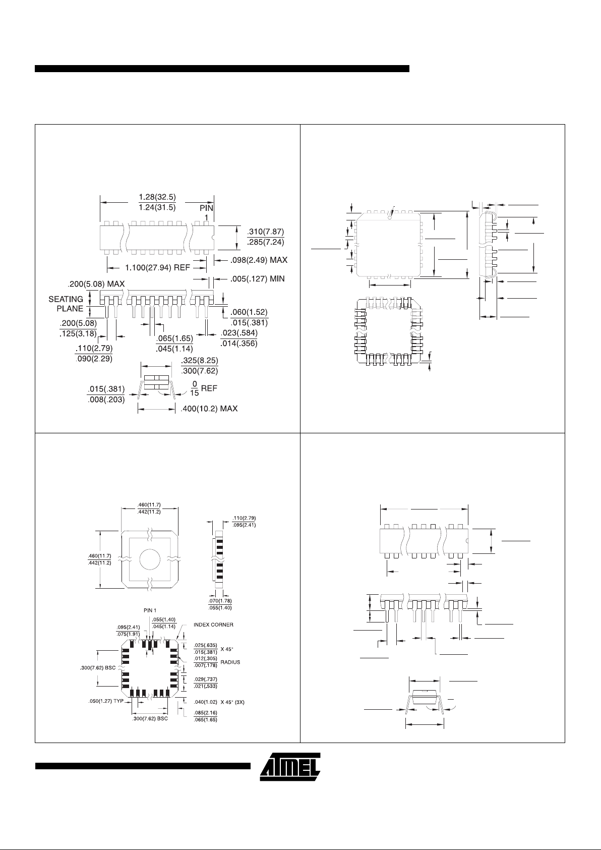
Package Type
24DW3 24-Lead, 0.300" Wide, Windowed, Ceramic Dual Inline Package (Cerdip)
28J 28-Lead, Plastic J-Leaded Chip Carrier OTP (PLCC)
28LW 28-Pad, Windowed, Ceramic Leadless Chip Carrier (LCC)
24P3 24-Lead, 0.300" Wide, Plastic Dual Inline Package OTP (PDIP)
24S 24-Lead, 0.300" Wide, Plastic Gull Wing Small Outline OTP (SOIC)
ATV750B
15
Packaging Information
.045(1.14) X 45°
PIN NO.1
IDENTIFY
.032(.813)
.026(.660)
.050(1.27) TYP
.300(7.62) REF SQ
.045(1.14) X 30° - 45°
.022(.559) X 45° MAX (3X)
.012(.305)
.008(.203)
.021(.533)
.013(.330)
.430(10.9)
.390(9.91)
SQ
.043(1.09)
.020(.508)
.120(3.05)
.090(2.29)
.180(4.57)
.165(4.19)
.456(11.6)
.450(11.4)
.495(12.6)
.485(12.3)
SQ
SQ
*Controlling dimension: millimeters
1.27(32.3)
1.25(31.7)
PIN
1
.266(6.76)
.250(6.35)
.090(2.29)
MAX
.005(.127)
MIN
.070(1.78)
.020(.508)
.023(.584)
.014(.356)
.065(1.65)
.040(1.02)
.325(8.26)
.300(7.62)
0
15
REF
.400(10.2) MAX
.012(.305)
.008(.203)
.110(2.79)
.090(2.29)
.151(3.84)
.125(3.18)
SEATING
PLANE
.200(5.06)
MAX
1.100(27.94) REF
24DW3
, 24-Lead, 0.300" Wide, WIndowed, Ceramic
Dual Inline Package (Cerdip)
Dimensions in Inches and (Millimeters)
MIL-STD-1835 D-9 CONFIG A
28J
, 28-Lead, Plastic J-Leaded Chip Carrier (PLCC)
Dimensions in Inches and (Millimeters)
JEDEC STANDARD MS-018 AB
28LW
, 28-Pad, Windowed, Ceramic Leadless Chip
Carrier (LCC)
Dimensions in Inches and (Millimeters)*
MIL-STD-1835 C-4
24P3
, 24-Lead, 0.300" Wide, Plastic Dual Inline
Package (PDIP)
Dimensions in Inches and (Millimeters)
JEDEC STANDARD MS-001 AF

Packaging Information
.020(.508)
.013(.330)
.299(7.60)
.291(7.39)
.420(10.7)
.393(9.98)
.105(2.67)
.092(2.34)
.050(1.27) BSC
.616(15.6)
.598(15.2)
.012(.305)
.003(.076)
.013(.330)
.009(.229)
.050(1.27)
.015(.381)
8
0
REF
PIN 1 ID
24S
, 24-Lead, 0.300" Wide, Plastic Gull Wing Small
Outline (SOIC)
Dimensions in Inches and (Millimeters)
© Atmel Corporation 1998.
Atmel Corporation makes no warranty for the use of its products, other than those expressly contained in the
Company’s standard warranty which is detailed in Atmel’s Terms and Conditions located on the Company’s
website. The Company assumes no responsibility for any errors which may appear in this document, reserves
the right to change devices or specifications detailed herein at any time without notice, and does not make any
commitment to update the information contained herein. No licenses to patents or other intellectual property of
Atmel are granted by the Company in connection with the sale of Atmel products, expressly or by implication. Atmel’s products are not
authorized for use as critical components in life support devices or systems.
Atmel Headquarters, 2325 Orchard Parkway, San Jose, CA 95131, TEL (408) 441-0311, FA X (408) 487-2600
Atmel Colorado Springs, 1150 E. Cheyenne Mtn. Blvd., Colorado Springs, CO 80906, TEL (719) 576-3300, FAX (719) 540-1759
Atmel Rousset, Zone Industrielle, 13106 Rousset Cedex, France, TEL (33) 4 42 53 60 00, FAX (33) 4 42 53 60 01
Marks bearing
®
and/or ™ are registered trademarks and trademarks of Atmel Corporation.
Ter ms and product names in this document may be trademarks of others.
Printed on recycled paper.
0301D–05/98/xM
 Loading...