

Using the ATV750 and ATV750B
Introduction
BDTIC www.bdtic.com/Semiconductor
This application note des cribes ho w to
use the features of the ATV750 and
ATV750B in the ABEL (and AtmelABEL) and CUPL (and Atmel-CUPL)
high level de scription lang uages. The
ATV750 and ATV750B are easy
upgrades from a 22V10. They offer twice
the logic densi ty and more fle xibility in
the same footprint. Both devices have 20
registers and individual clock and AR
product terms for each register. Each I/O
pin has a programmable polarity control
and an individual output enable product
term. Independent feedback paths fr om
each register allow all of the registers to
Table 1. Device Names
Device Type ABEL Device Name CUPL Device Name
ATV750 DIP P750 V750
ATV750 PLCC P750C V750LCC
ATV750B DIP P750B V750B
ATV750B PLCC P750BC V750BLCC
be buried without wasting the I/O pins.
For the ATV750B the registers can also
be configured as D- or T-type and the
clock can be selected as either a synchronous clock pin or a clock product
term. The ATV750 and ATV750B macrocell is shown in Figure 1.
Device Names and Pin and
Node Assignments
The device names for the ATV750 an d
ATV750B for each langu age are shown
in Table 1.
Erasable
Programmable
Logic Device
Application
Note
Table 2. Node Numbers
ABEL CUPL
Pin #
14(17) 26 (30) 25 (29) 35 (39)
15(18) 27 (31) 26 (30) 36 (40)
16(19) 28 (32) 27 (31) 37 (41)
17(20) 29 (33) 28 (32) 38 (42)
18(21) 30 (34) 29 (33) 39 (43)
19(23) 31 (35) 30 (34) 40 (44)
20(24) 32 (36) 31 (35) 41 (45)
21(25) 33 (37) 32 (36) 42 (46)
22(26) 34 (38) 33 (37) 43 (47)
23(27) 35 (39) 34 (38) 44 (48)
Note: Pin/node numbers: DIP (PLCC)
Q1 Q1 Q0
Rev. 0459C–09/99
1
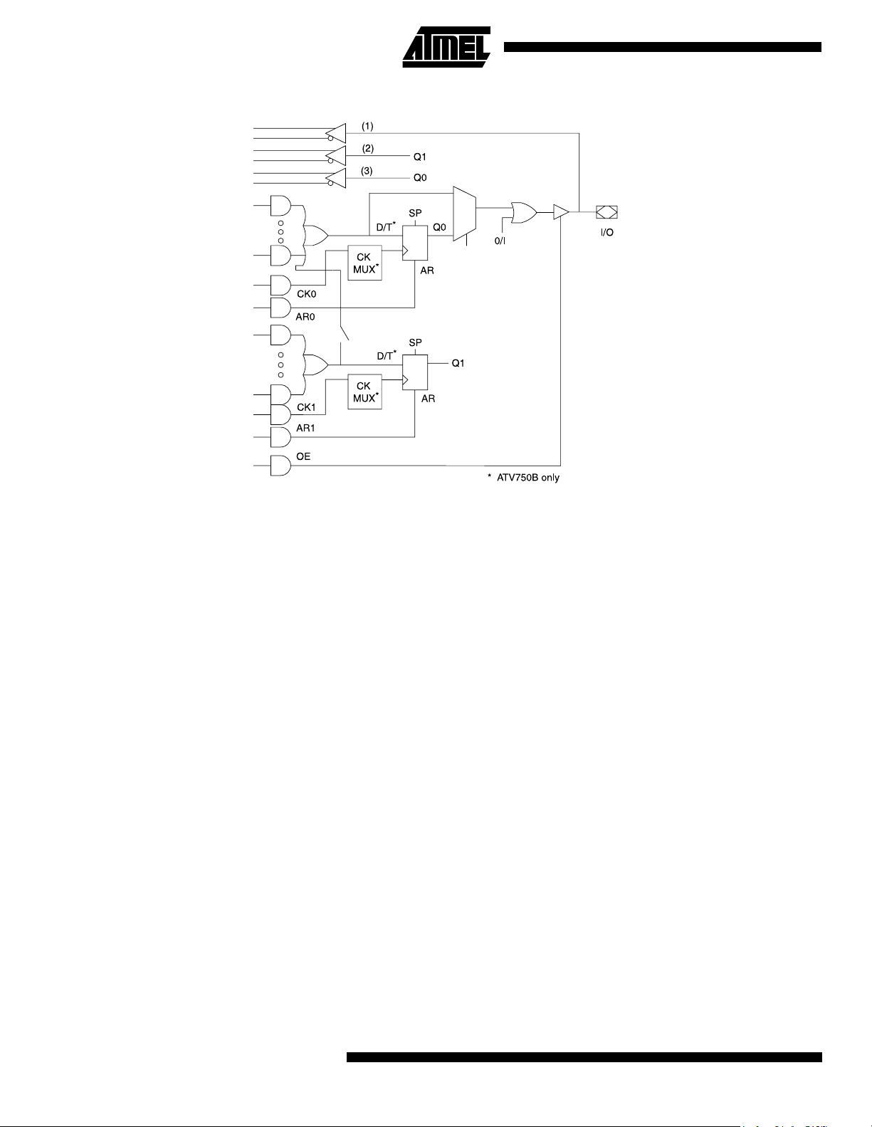
Figure 1. The ATV750 and ATV750B Macroce l l
Buried registers (Q1 in each mac rocell) are identified by
node numbers. Table 2 shows the node numbers for the
Q1 registers in the ATV750 and ATV750B. Registers which
are associated with the I/O pin (Q0 in each macrocell) are
identified by the pin numbers. The use of the Q0 node numbers in CUPL is described in the Macrocell Configurations
section.
The following ex amples s how the de vice type specif icatio n
and the pin and node assignments:
ABEL and Atmel-ABEL
device_id device ’P750B’; “device_id will be used
”for JEDEC filename
I1,I2,I3,I4,I5 pin 1,2,3,4,5;
O23,O22 pin 23,22 istype 'reg_d,buffer';
O21,O20 pin 21,20 istype 'com';
O23Q1,O20Q1 node 35,32 istype 'reg_d';
CUPL and Atmel-CUPL
device V750B;
pin [1,2,3,4,5] = [I1,I2,I3,I4,I5];
pin [20,21,22,23] = [O20,O21,O22,O23];
pinnode [34,44,31] = [O23Q1,O23Q0,O20Q1];
Pin and Node Feedbacks
Each macrocell has three feedback paths into the array,
one from each of the registers and one from the pin. For a
buried register, th e node name is u sed to refer to th e
feedback path. For a combinatoria l output, the feedb ack
comes from the pin, so th e pin name is used to refer to th e
feedback. For a registered output, the feedback can come
either from the register or from the pin. The feedback paths
are labeled (1), (2), and (3) on Figure 1. The following
examples show how the different feedback paths are
identified:
ABEL and Atmel-ABEL
O23.d = I1 # I2;
O23Q1.d = I1 & !I2;
O21 = O23 “(1)feedback from pin
# O23.fb “(2)feedback from Q0 register
# O23Q1; “(3)feedback from buried register
Note: 1. For ABEL, either “.q” or “.fb” can be used to indicate
the buried register feedback path. When “.q” extension is used, the software will select the Q outp ut of
the register, regardless of the output buffer polarity.
When the “.fb” extension is used, the software will
match the polarity of the register feedback with the
output polarity by selecting either the Q or !Q output
of the register.
(1)
CUPL and Atmel-CUPL
O23.d = I1 # I2;
O23Q1.d = I1 & !I2;
O21 = O23.io /*(1)feedback from pin */
# O23 /*(2)feedback from Q0 register */
# O23Q1; /*(3)feedback from buried register */
2
CMOS PLD
Macrocell Configurations
CMOS PLD
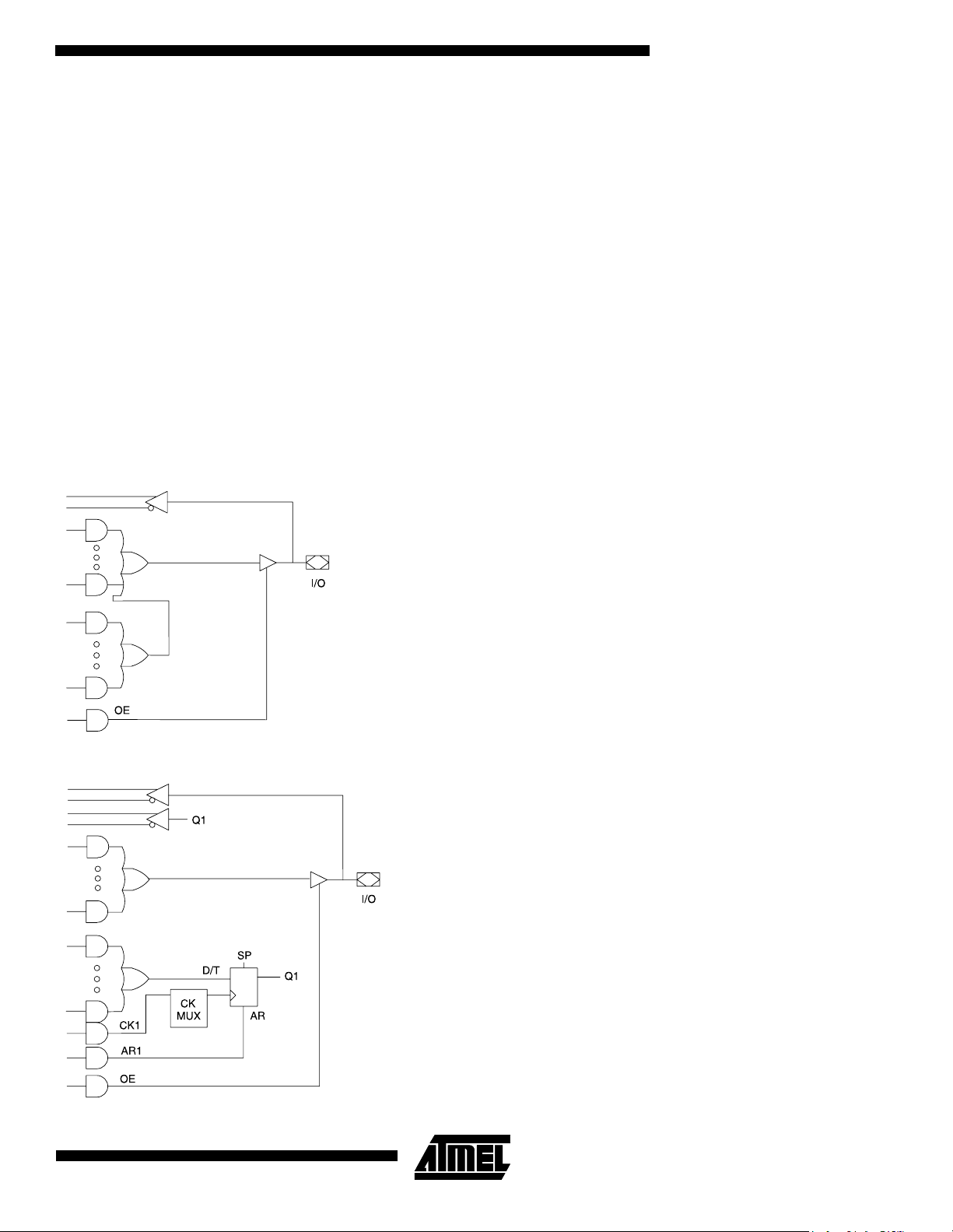
The basic m acroc ell co nfig ura tions are sh own i n Fi gur es 2
through 7. Each macrocell can be configured as either a
registered or combinatorial output. In addition, each macrocell has a buried register. The multiple feedback paths also
allow both registers to be bur ied, with th e I/O pin used as
an input pin.
The macrocells h ave a t otal of b etween 8 a nd 16 pr oduct
terms. If the buried register is used, the product terms are
automatically divided into two sum terms, each with half of
the product ter ms. If the bu ried register is not used, all o f
the product terms are available for the I/O function.
For ABEL, the Q1 register is identified by a node number.
The Q0 register is identif ied by the pin numb er. The OE
should be set to 0 to disable the outputs. The “pinname”
(with no extensions) refers to the input path. The “pin-
name.fb” refers to the register feedback path. Another
Figure 2. Combinatorial Output
name for either th e inpu t o r the register may be substi tute d
in the Declarations section of the file, to make it clearer that
they have separate functions . The pi n and no de nam es wil l
be substituted back into the equations when the file is
compiled.
For CUPL, there are node numbers for both the Q1 and Q0
registers. The Q0 node numbers sho uld onl y b e us ed if th e
Q0 register is buried and the pin is used as an inp ut. The
Q0 node name refers to the register and the pin name
refers to the pin.
For this configuration, the output should be defined as combinatorial, and the equation written as combi natorial. A
clock equation should also be written for the output. The
registered signal which is fed back into the array is identified with “.fb” or “.q” for ABEL or “.dfb” for CUPL.
ABEL and Atmel-ABEL
O21 = I1 # !I2 # I3 # !I4 # I5;
CUPL and Atmel-CUPL
O21 = I1 # !I2 # I3 # !I4 # I5;
Figure 3. Combinatorial Output plus Buried Register
ABEL and Atmel-ABEL
O20 = I3 & !I4;
O20Q1.d = I2 # I3 # I4;
CUPL and Atmel-CUPL
O20 = I3 & !I4;
O20Q1.d = I2 # I3 # I4;
3
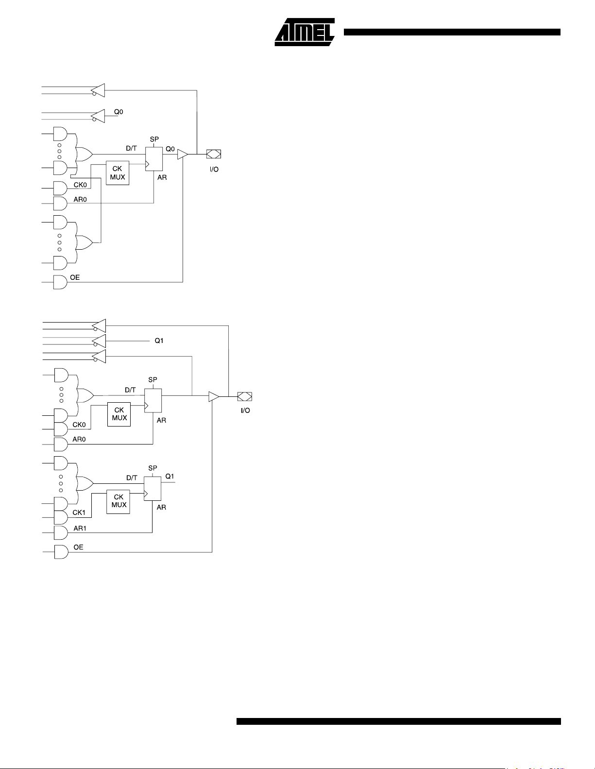
Figure 4. Registered Output
Figure 5. Registered Output plus Buried Register
ABEL and Atmel-ABEL
O23.d = I1 # I2 # I3 # I4 # I5;
CUPL and Atmel-CUPL
O23.d = I1 # I2 # I3 # I4 # I5;
ABEL and Atmel-ABEL
O23.d = I1 & I2;
O23Q1.d = I3 & I4;
CUPL and Atmel-CUPL
O23.d = I1 & I2;
O23Q1.d = I3 & I4;
4
CMOS PLD

Figure 6. Both Registers Buried, I/O Pin Used as Input
CMOS PLD
ABEL and Atmel-ABEL
Declarations
O23 pin 23 istype 'reg_d';
O23Q1 node 35 istype 'reg_d';
INPUT_FUNC = O23;
REG_FUNC = O23.fb;
Equations
O23.d = INPUT_FUNC & I3;
O23.oe = 0; “disable OE to use pin for input
O23Q1.d = REG_FUNC & I4;
CUPL and Atmel-CUPL
pin 23 = O23;
pinnode [34,44] = [O23Q1,O23Q0];
O23Q0.d = O23 & I3;
O23.oe = 'b'0; /*disable OE to use pin for */
/*input */
O23Q1.d = O23Q0 & I4;
Figure 7. Combinatorial Output, Q0 Register Used to Latch Data
ABEL and Atmel-ABEL
O21 = I3;
O21.ck = CLK;
O23.d = O21.fb; “registered O21 output
CUPL and Atmel-CUPL
O21 = I3;
O21.ck = CLK;
O23.d = O21.fb; /* registered O21 output */
Asynchronous Reset, Synchronous Preset and Output Enable
There is an indivi dual as ynchro nous res et produ ct term for
each register. A s ingle sync hronou s preset product te rm is
used to preset all registers. Since the synchronous preset
requires a clock, an individual register will only preset if it is
clocked. Each I/O pin has an individual output enable product term. The following examples show how the
asynchronous reset, synchronous preset, and output
enable functions are defined:
ABEL and Atmel-ABEL
O23.ar = I1;
O23.sp = I2; “NOTE: preset is for all registers
O23.oe = I3 & I4;
O22.oe = 1;
CUPL and Atmel-CUPL
O23.ar = I1;
O23.sp = I2; /*NOTE: preset is for all registers*/
O23.oe = I3 & I4;
O22.oe = 'b'1;
5

Programmable Polarity Control
D-type or T-type Registers
Each I/O pin has pr ogrammabl e polarity con trol. Pleas e
refer to the application note “Using the Programmable
Polarity Control” for details on using the polarity control.
Clock Options
For the ATV750, each register has an independent clock
product term. For the ATV750B, each register can be configured to use either the clock product term or a
synchronous clock pin (see Figure 8).
Figure 8. Clock Options
The following examples show how the clock is defined for
the two different modes:
ABEL and Atmel-ABEL
SYNC_CLK pin 1;
ASYNC_CLK,EN pin 2,3;
O23.ck = SYNC_CLK; “clock assigned to pin 1,
“no clock equation,
“software selects
“synchronous clock pin
“(for ATV750B only)
O23Q1.ck = ASYNC_CLK; “clock assigned to pin 2,
“software selects clock
“product term
O22.ck = ASYNC_CLK & EN; “clock uses product term,
“software selects clock
“product term
For the ATV750, the registers can only be configured as
D-type flip-flops. For the ATV750B, the registers can be
configured as eithe r D-type or T-typ e flip-f lops. The foll owing examples show ho w to co nfi gur e th e re g ister s as eit her
D- or T-type:
ABEL and Atmel-ABEL
O13 pin 13 istype 'reg_t';
O23.d = I1 & I2;
O13.t = I1 # I2;
CUPL and Atmel-CUPL
pin 13 = O13;
O23.d = I1 & I2;
O13.t = I1 # I2;
Design Example
Figure 9 shows a watchdog timer circuit which is implemented in an ATV750B. The circuit detects whether an
event occurs at a regular in terva l. For this desig n, the ti mer
is set to detect whether the WATCHDOGL input goes low
every 18 ms. An 8 bit counter running on a 1ms clock
counts the number of clock cycles between events. A small
state machine detects whether the event occurs within the
expected window. If the event occurs either too soon or too
late, an error is generated. If the event occurs during the
window, the counter is reset to time the next event.
The ABEL and CUPL descriptions for this design follow.
Figure 9. Design Example
CUPL and Atmel-CUPL
pin 1 = SYNC_CLK;
pin [2,3] = [ASYNC_CLK,EN];
O23.ckmux = SYNC_CLK; /*.ckmux extension */
/*selects synchronous */
/*clock pin */
/*(for ATV750B only) */
O23Q1.ck = SYNC_CLK; /*.ck extension selects */
O22.ck = ASYNC_CLK & EN;
6
/*clock product term */
CMOS PLD

Example ABEL Description File
module WATCH;
title ’Watchdog Timer V750B Design Example
ATMEL Corporation March 27, 1995’;
WATCH device ’P750B’;
CLK1,WATCHDOGL,PORL pin 1,2,3;
RESET,CLEARCOUNT pin 23,22 istype ’com,buffer’;
ERRPULSE,ERRPULSE2 pin 21,20 istype ’reg_d,buffer’;
WDOG,WDOG2 pin 17,16 istype ’reg_d,buffer’;
Q0,Q1,Q2,Q3,Q4,Q5,Q6,Q7 node 35,34,33,32,29,28,27,26 istype ’reg_t’;
REGA, REGB pin 18,19 istype ’reg_d,buffer’;
COUNT8 = [Q7..Q0]; "8-bit counter
H,L,Z,C,K,X,U,D = 1,0,.Z.,.C.,.K.,.X.,.U.,.D.;
"Define state values
POWERUP = ^B00;
IDLE = ^B10;
WAIT = ^B01;
ERROR = ^B11;
CMOS PLD
STATE_MACH = [REGB,REGA];
"Internal counter values used in state machine
" (these are 1 less than actual due to state machine delay)
LT18 = (COUNT8 < 16);
GT22 = (COUNT8 > 20);
MS256 = (COUNT8 == 255);
IRESET = (STATE_MACH == ERROR);
Equations
" For WATCHDOGL input, generate a 1 clock cycle wide pulse.
" Uses opposite edge of system clock from the state machine to
" insure that there are no setup or metastability problems between
" the inputs to the state machine and the state machine clock.
WDOG.d = (!WATCHDOGL & !WDOG2.fb);
WDOG2.d = (!WATCHDOGL);
WDOG.ck = !CLK1;
WDOG2.ck = !CLK1;
WDOG.ar = !PORL;
WDOG2.ar = !PORL;
" Generate 1 clock cycle wide error pulse upon entering ERROR
" state. Uses opposite clock edge from state machine to ensure
" error pulse generation is clean.
ERRPULSE.d = (IRESET & !ERRPULSE2.fb);
ERRPULSE2.d = IRESET;
ERRPULSE.ck = !CLK1;
ERRPULSE2.ck = !CLK1;
ERRPULSE.ar = !PORL;
ERRPULSE2.ar = !PORL;
7

"256mS Internal Timer
" (resets on power-up reset, watchdog input, or ERROR state)
CLEARCOUNT = (!PORL # WDOG # ERRPULSE.fb);
COUNT8.ck = CLK1;
COUNT8.ar = CLEARCOUNT;
COUNT8.t = (COUNT8 + 1) $ COUNT8;
RESET = (!PORL # IRESET); "external RESET output
"State machine clocks and resets
STATE_MACH.ck = CLK1;
STATE_MACH.ar = !PORL;
state_diagram STATE_MACH;
state POWERUP:
if (WDOG & !MS256) then IDLE;
else if (MS256) then ERROR;
else POWERUP;
state IDLE:
if (WDOG) then ERROR;
else if (!LT18) then WAIT;
else IDLE;
state WAIT:
if (WDOG) then IDLE;
else if (!WDOG & GT22) then ERROR;
else WAIT;
state ERROR:
if (MS256) then POWERUP;
else ERROR;
"Test normal powerup and normal watchdog input
TEST_VECTORS (
[CLK1, PORL,WATCHDOGL] -> [STATE_MACH,COUNT8,RESET])
[ U, 0, X ] -> [POWERUP, 0, 1 ];
[ K, 1, 1 ] -> [POWERUP, 1, 0 ];
[ K, 1, 1 ] -> [POWERUP, 2, 0 ];
[ K, 1, 1 ] -> [POWERUP, 3, 0 ];
[ K, 1, 0 ] -> [IDLE, 0, 0 ];
@@CONST CNT = 0;
@@REPEAT 9 {
@@CONST CNT = CNT + 1;
[ K, 1, 0 ] -> [ IDLE, CNT, 0 ];}
@@REPEAT 7 {
@@CONST CNT = CNT + 1;
[ K, 1, 1 ] -> [IDLE, CNT, 0 ];}
[ K, 1, 1 ] -> [WAIT, 17, 0 ];
[ K, 1, 1 ] -> [WAIT, 18, 0 ];
[ K, 1, 1 ] -> [WAIT, 19, 0 ];
[ K, 1, 0 ] -> [IDLE, 0, 0 ];
[ K, 1, 0 ] -> [IDLE, 1, 0 ];
[ K, 1, 0 ] -> [IDLE, 2, 0 ];
"Now test various state transitions and timeouts
TEST_VECTORS (
[CLK1, PORL,WATCHDOGL] -> [STATE_MACH,COUNT8,RESET])
[ U, 0, X ] -> [POWERUP, 0, 1 ];
[ K, 1, 1 ] -> [POWERUP, 1, 0 ];
[ K, 1, 1 ] -> [POWERUP, 2, 0 ];
[ K, 1, 1 ] -> [POWERUP, 3, 0 ];
[ K, 1, 0 ] -> [IDLE, 0, 0 ];
8
CMOS PLD

@@CONST CNT = 0;
@@REPEAT 15 {
@@CONST CNT = CNT + 1;
[ K, 1, 1 ] -> [IDLE, CNT, 0 ];
[ K, 1, 1 ] -> [IDLE, 16, 0 ];
[ K, 1, 1 ] -> [WAIT, 17, 0 ];
[ K, 1, 1 ] -> [WAIT, 18, 0 ];
[ K, 1, 1 ] -> [WAIT, 19, 0 ];
[ K, 1, 1 ] -> [WAIT, 20, 0 ];
[ K, 1, 1 ] -> [WAIT, 21, 0 ];
[ K, 1, 1 ] -> [ERROR, 22, 1 ]; "Input doesn’t happen
[ K, 1, 1 ] -> [ERROR, 0, 1 ];
[ K, 1, 1 ] -> [ERROR, 1, 1 ];
[ K, 0, X ] -> [POWERUP, 0, 1 ]; "RESET
[ K, 1, 1 ] -> [POWERUP, 1, 0 ];
[ K, 1, 0 ] -> [IDLE, 0, 0 ];
[ K, 1, 1 ] -> [IDLE, 1, 0 ];
[ K, 1, 0 ] -> [ERROR, 0, 1 ]; "Input hits too soon
[ K, 1, 1 ] -> [ERROR, 0, 1 ];
[ K, 1, 1 ] -> [ERROR, 1, 1 ];
[ U, 0, 1 ] -> [POWERUP, 0, 1 ];
@@REPEAT 255 { "Test POWERUP timeout
[ K, 1, 1 ] -> [POWERUP, X, 0 ];
@@REPEAT 257 { "Test ERROR timeout
[ K, 1, 1 ] -> [ ERROR, X, 1 ];
[ K, 1, 1 ] -> [POWERUP, X, 0 ];
[ K, 1, 1 ] -> [POWERUP, X, 0 ];
[ K, 1, 1 ] -> [POWERUP, X, 0 ];
CMOS PLD
END WATCH;
9

Example CUPL Description File
Name WATCH;
Partno N/A;
Date 3/27/95;
Rev. -;
Designer PLD Expert;
Company Atmel;
Assembly -;
Location -;
Device V750B;
pin [1,2,3] = [CLK1,WATCHDOGL,PORL];
pin [23,22] = [RESET,CLEARCOUNT];
pin [21,20] = [ERRPULSE,ERRPULSE2];
pin [17,16] = [WDOG,WDOG2];
pin [18,19] = REGA, REGB;
pinnode [34,33,32,31,28,27,26,25] = [Q0..Q7];
field COUNT8 = [Q7..Q0]; /* 8-bit counter */
/* Define state values */
$define POWERUP ’b’00
$define IDLE ’b’10
$define WAIT ’b’01
$define ERROR ’b’11
field STATE_MACH = [REGB,REGA];
/* Internal counter values used in state machine */
/* (these are 1 less than actual due to state machine delay) */
LT18 = COUNT8:[0..F];
GT22 = COUNT8:[15..FF];
MS256 = COUNT8:FF;
IRESET = STATE_MACH:ERROR;
/* Equations */
/* For WATCHDOGL input, generate a 1 clock cycle wide pulse.
Uses opposite edge of system clock from the state machine to
insure that there are no setup or metastability problems between
the inputs to the state machine and the state machine clock. */
WDOG.d = (!WATCHDOGL & !WDOG2);
WDOG2.d = (!WATCHDOGL);
WDOG.ck = !CLK1;
WDOG2.ck = !CLK1;
WDOG.ar = !PORL;
WDOG2.ar = !PORL;
/* Generate 1 clock cycle wide error pulse upon entering ERROR
state. Uses opposite clock edge from state machine to ensure
error pulse generation is clean. */
ERRPULSE.d = (IRESET & !ERRPULSE2);
ERRPULSE2.d = IRESET;
ERRPULSE.ck = !CLK1;
ERRPULSE2.ck = !CLK1;
ERRPULSE.ar = !PORL;
ERRPULSE2.ar = !PORL;
10
CMOS PLD

/* 256mS Internal Timer
(resets on power-up reset, watchdog input, or ERROR state) */
CLEARCOUNT = (!PORL # WDOG # ERRPULSE);
COUNT8.ck = CLK1;
COUNT8.ar = CLEARCOUNT;
Q0.t = ’b’1;
Q1.t = Q0;
Q2.t = Q1 & Q0;
Q3.t = Q2 & Q1 & Q0;
Q4.t = Q3 & Q2 & Q1 & Q0;
Q5.t = Q4 & Q3 & Q2 & Q1 & Q0;
Q6.t = Q5 & Q4 & Q3 & Q2 & Q1 & Q0;
Q7.t = Q6 & Q5 & Q4 & Q3 & Q2 & Q1 & Q0;
RESET = (!PORL # IRESET); /* external RESET output */
/* State machine clocks and resets */
STATE_MACH.ck = CLK1;
STATE_MACH.ar = !PORL;
sequence STATE_MACH {
present POWERUP
if (WDOG & !MS256) next IDLE;
if (MS256) next ERROR;
default next POWERUP;
present IDLE
if (WDOG) next ERROR;
if (!WDOG & !LT18) next WAIT;
default next IDLE;
present WAIT
if (WDOG) next IDLE;
if (!WDOG & GT22) next ERROR;
default next WAIT;
present ERROR
if (MS256) next POWERUP;
default next ERROR;
}
CMOS PLD
CUPL Simulation Input File (WATCH.SI)
Name WATCH;
Partno N/A;
Date 3/27/95;
Rev. -;
Designer PLD Expert;
Company Atmel;
Assembly -;
Location -;
Device V750B;
ORDER: CLK1,%1,PORL,%1,WATCHDOGL,%2,STATE_MACH,%1,COUNT8,%1,RESET;
BASE: decimal;
VECTORS:
$MSG “Test normal powerup and normal watchdog input”;
1 0 X “0" ”0" H
K 1 1 “0" ”1" L
K 1 1 “0" ”2" L
K 1 1 “0" ”3" L
K 1 0 “2" ”0" L
$REPEAT 9;
K 1 0 “2" ”*" L
11

$REPEAT 7;
K 1 1 “2" ”*" L
K 1 1 “1" ”17" L
K 1 1 “1" ”18" L
K 1 1 “1" ”19" L
K 1 0 “2" ”0" L
K 1 0 “2" ”1" L
K 1 0 “2" ”2" L
$MSG “Test various state transitions and timeouts”;
1 0 X “0" ”0" H
K 1 1 “0" ”1" L
K 1 1 “0" ”2" L
K 1 1 “0" ”3" L
K 1 0 “2" ”0" L
$REPEAT 15;
K 1 1 “2" ”*" L
K 1 1 “2" ”16" L
K 1 1 “1" ”17" L
K 1 1 “1" ”18" L
K 1 1 “1" ”19" L
K 1 1 “1" ”20" L
K 1 1 “1" ”21" L
K 1 1 “3" ”22" H /*Input doesn't happen*/
K 1 1 “3" ”0" H
K 1 1 “3" ”1" H
K 0 X “0" ”0" H /*RESET*/
K 1 1 “0" ”1" L
K 1 0 “2" ”0" L
K 1 1 “2" ”1" L
K 1 0 “3" ”0" H /*Input hits too soon*/
K 1 1 “3" ”0" H
K 1 1 “3" ”1" H
1 0 1 “0" ”0" H
$REPEAT 255; /*Test POWERUP timeout*/
K 1 1 “0" ”*" L
$REPEAT 257; /*Test ERROR timeout*/
K 1 1 “3" ”*" H
K 1 1 “0" ”*" L
K 1 1 “0" ”*" L
K 1 1 “0" ”*" L
12
BDTIC www.bdtic.com/Semiconductor
CMOS PLD
 Loading...