

BDTIC www.bdtic.com/Semiconductor
BDTIC 中国领先的半导体集成电路代理商
Using the ATV2500 and ATV2500B
Introduction
This application note des cribes ho w to
use the features of the ATV2500 and
ATV2500B in the ABEL (and AtmelABEL) and CUPL (and Atmel-CUPL)
high level de scription lang uages. The
ATV2500 and ATV2500B are the most
powerful programmable logic devices
available in a 40/44-pin package. They
combine high dens ity and globa l rout ing,
making them easy to use and understand. Both devi ces h ave 24 macr ocells ,
each with three sum terms, two registers, and 17 product terms. Each register
has individual cl ock and AR product
terms. Each I/O pin has a programmable
polarity contro l and an individ ual output
enable product term. Independent feedback paths from each register allow all of
the registers to be buried without wasting
the I/O pins. A universal bus routes all
input and feedbac k si gnals to a ll pr oduct
terms on all macrocells. The ATV2500B
has the additional features of D- or
T-type configurable registers, three different clock options, and buried
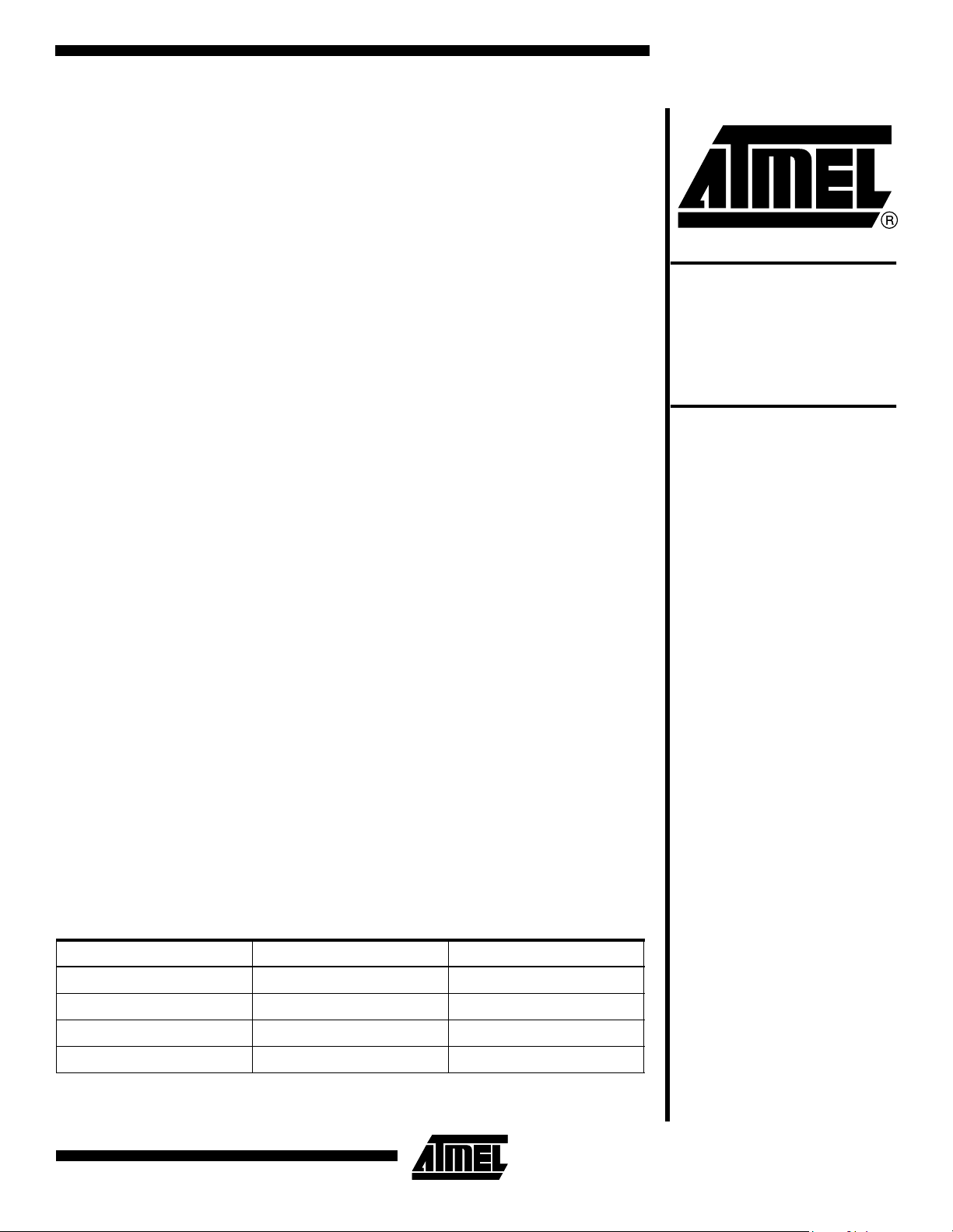
combinatorial nodes. The ATV2500 and
ATV2500B macrocell is shown in
Figure 1.
Device Names and Pin and Node Assignments
The device names for the ATV2500 and
ATV2500B for each language are shown
in Table 1.
The buried nodes (Q1 and Q2/F2 in
each macrocell) are identified by node
numbers, as shown in Table 2.
The following exampl es show t he devi ce
type specification and the pin and node
assignments:
ABEL and Atmel-ABEL
device_id device ‘P2500B’;
“device_id will be used for
“JEDEC filename
I1,I2,I3,I17,I18 pin 1,2,3,17,18;
O4,O5 pin 4,5 istype ‘reg_d,buffer’;
O6,O7 pin 6,7 istype ‘com’;
O4Q2,O7Q2 node 41,44 istype ‘reg_d’;
O6F2 node 43 istype ‘com’;
O7Q1 node 220 istype ‘reg_d’;
CUPL and Atmel-CUPL
device V2500B;
pin [1,2,3,17,18] =
[I1,I2,I3,I17,I18];
pin [7,6,5,4] = [O7,O6,O5,O4];
pinnode [41,65,44] =
[O4Q2,O4Q1,O7Q2];
pinnode [43,68] = [O6Q2,O7Q1];
Erasable
Programmable
Logic Device
Application
Note
Table 1. Device Names
Device Type ABEL Device Name CUPL Device Name
ATV2500 DIP P2500 V2500
ATV2500 PLCC P2500C V2500LCC
ATV2500B DIP P2500B V2500B
ATV2500B PLCC P2500BC V2500BLCC
Rev. 0458C–09/99
1
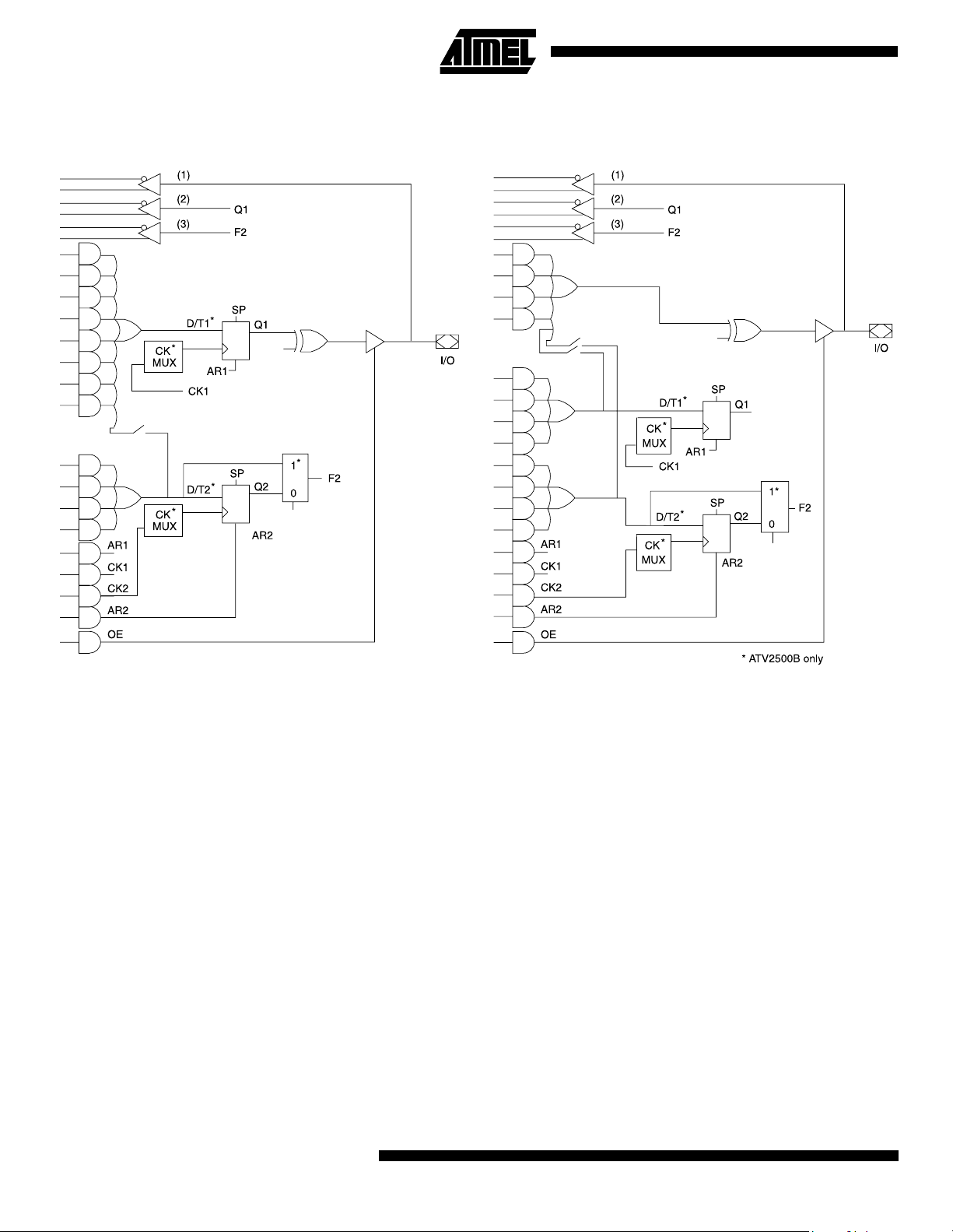
Figure 1. The ATV2500 and ATV2500B
Macrocell Output Logic, Registered Output Logic, Combinatorial
Pin and Node Feedbacks
Each macrocell has three feedback paths into the array,
one from each of the registers and one from the pin. For a
buried node, the node name is used to refer to the feedback path. For a comb in ator i al outp ut, t he feedback comes
from the pin, so the pin name is used to refer to the feedback. For a registered output, the feedback can come
either from the register or from the pin. The feedback paths
are labeled (1), (2), and (3) on Figure 1. The following
examples show how the different feedback paths are
identified:
ABEL and Atmel-ABEL
O4.d = I1 # I2;
O4Q2.d = I1 & !I2;
O6 = O4 “(1)feedback from pin
# O4.fb “(2)feedback from Q1 register
# O4Q2; “(3)feedback from buried register
2
CMOS PLD
(1)
Note: 1. For ABEL, either “.q” or “.fb” can be used to indicate
the buried register feedback path. When “.q” extension is used, the software will select the Q outp ut of
the register, regardless of the output buffer polarity.
When the “.fb” extension is used, the software will
match the polarity of the register feedback with the
output polarity by selecting either the Q or !Q output
of the register.
CUPL and Atmel-CUPL
O4.d = I1 # I2;
O4Q2.d = I1 & !I2;
O6 = O4.io /*(1)feedback from pin */
# O4 /*(2)feedback from Q1 register */
# O4Q2; /*(3)feedback from buried register */

Table 2. Node Numbers
CMOS PLD
ABEL CUPL
Pin #
4(5) 217(221) 41(45) 65(69) 41(45)
5(6) 218(222) 42(46) 66(70) 42(46)
6(7) 219(223) 43(47) 67(71) 43(47)
7(8) 220(224) 44(48) 68(72) 44(48)
8(9) 221(225) 45(49) 69(73) 45(49)
9(10) 222(226) 46(50) 70(74) 46(50)
11(13) 223(227) 47(51) 71(75) 47(51)
12(14) 224(228) 48(52) 72(76) 48(52)
13(15) 225(229) 49(53) 73(77) 49(53)
14(16) 226(230) 50(54) 74(78) 50(54)
15(17) 227(231) 51(55) 75(79) 51(55)
16(18) 228(232) 52(56) 76(80) 52(56)
24(27) 229(233) 53(57) 77(81) 53(57)
25(28) 230(234) 54(58) 78(82) 54(58)
26(29) 231(235) 55(59) 79(83) 55(59)
27(30) 232(236) 56(60) 80(84) 56(60)
28(31) 233(237) 57(61) 81(85) 57(61)
Q1 Q2/F2 Q1 Q2/F2
29(32) 234(238) 58(62) 82(86) 58(62)
31(35) 235(239) 59(63) 83(87) 59(63)
32(36) 236(240) 60(64) 84(88) 60(64)
33(37) 237(241) 61(65) 85(89) 61(65)
34(38) 238(242) 62(66) 86(90) 62(66)
35(39) 239(243) 63(67) 87(91) 63(67)
36(40) 240(244) 64(68) 88(92) 64(68)
Note: Pin/node numbers: DIP(PLCC)
3
Macrocell Configurations
The basic m acroc ell co nfig ura tions are sh own i n Fi gur es 2
through 9. Each ma crocel l has thre e sum terms , each w ith
four product terms. The sum terms can b e combined for
wider fan-in functions or separated and used for buried
logic. The output ca n be conf igure d as eit her co mbinat orial
or registered. For a combinatorial output, the other two sum
terms can be connecte d to buried regi sters. For a r egis-
Figure 2. Combinatorial Output (12 product terms)
tered output, two of the sum ter ms are combin ed for the
output and the third can be connected to a buried register.
The multiple feedbac k path s als o a ll ow b oth reg is ter s to b e
buried, with the I/O pin used as an input pin. For the
ATV2500B, the Q2 node can also be configured as a buried combinatorial node, F2, as shown in Figu re 9.
ABEL and Atmel-ABEL
O6 = I1 # !I2 # I3 # !I17 # I18;
CUPL and Atmel-CUPL
O6 = I1 # !I2 # I3 # !I17 # I18;
Figure 3. Combinatorial Output (8 product terms) plus Buri ed Regi ste r (4 prod uct terms )
ABEL and Atmel-ABEL
O7 = I1 # !I2 # I3 # !I17 # I18;
O7Q2.d = I2 # I3 # I17;
CUPL and Atmel-CUPL
O7 = I1 # !I2 # I3 # !I17 # I18;
O7Q2.d = I2 # I3 # I17;
4
CMOS PLD
CMOS PLD
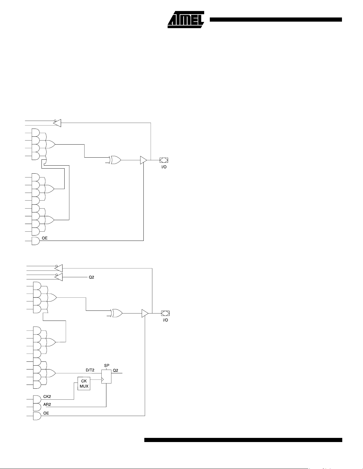
Figure 4. Combinatorial Output (4 product terms) plus 2 Buried Registers (4 product terms each)
ABEL and Atmel-ABEL
O7 = I3 & !I17;
O7Q1.d = I1 & I2
O7Q2.d = I2 # I3 # I17;
CUPL and Atmel-CUPL
O7 = I3 & !I17;
O7Q1.d = I1 & I2
O7Q2.d = I2 # I3 # I17;
Figure 5. Registered Output (12 product terms)
ABEL and Atmel-ABEL
O4.d = I1 # I2 # I3 # I17 # I18;
CUPL and Atmel-CUPL
O4.d = I1 # I2 # I3 # I17 # I18;
5

Figure 6. Registered Output (8 product terms) plus Buried Register (4 product terms)
ABEL and Atmel-ABEL
O4.d = I1 & I2;
O4Q2.d = I3 & I17;
CUPL and Atmel-CUPL
O4.d = I1 & I2;
O4Q2.d = I3 & I17;
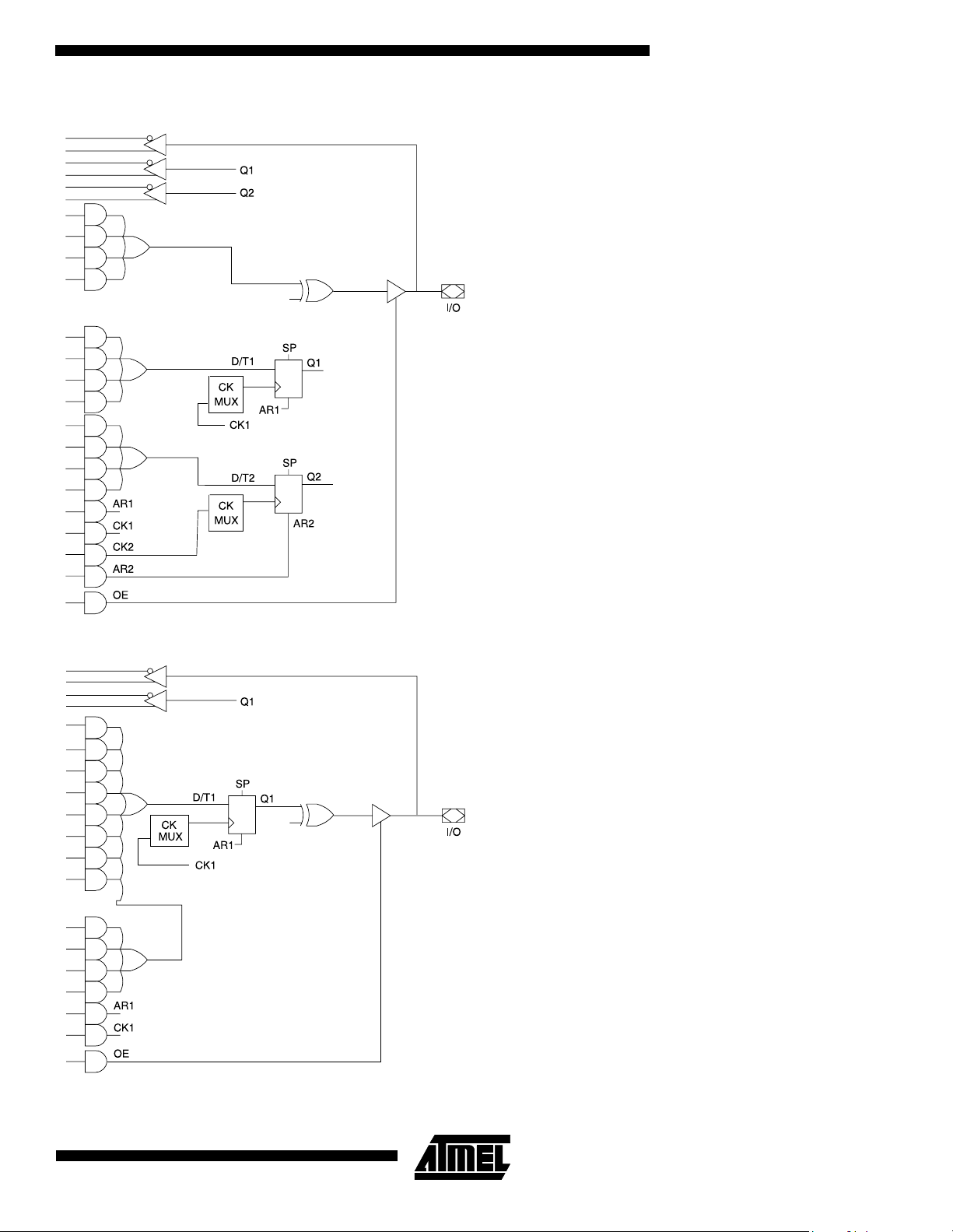
Figure 7. Both Registers Buried (Q1 - 8 product terms, Q2 - 4 product terms), I/O Pin Used as Input
ABEL and Atmel-ABEL
Declarations
O4 pin 4 istype ‘reg_d’;
O4Q2 node 41 istype ‘reg_d’;
INPUT_FUNC = O4;
REG_FUNC = O4.fb;
Equations
O4.d = INPUT_FUNC & I3;
O4.oe = 0; “disable OE to use pin for input
O4Q2.d = REG_FUNC & I17;
CUPL and Atmel-CUPL
pin 4 = O4;
pinnode [41,65] = [O4Q2,O4Q1];
O4Q1.d = O4 & I3;
O4.oe = ’b’0;/*disable OE to use pin for input */
O4Q2.d = O4Q0 & I17;
6
CMOS PLD

CMOS PLD
Figure 8. Combinatorial Output, Q1 Register Used to Latch Data
ABEL and Atmel-ABEL
O6 = I3;
O6.ck = CLK;
O4.d = O6.fb; “registered O6 output
CUPL and Atmel-CUPL
O6 = I3;
O6.ck = CLK;
O4.d = O6.fb; /* registered O6 output */
Figure 9. ATV2500B ONLY: Registered or Combinatorial Output plus Buried Combinatorial Node (4 product terms)
ABEL and Atmel-ABEL
Declarations
O4 pin 4 istype ‘reg_d’;
O4F2 node 41 istype ‘com’;
Equations
O4.d = I2 & I3;
O4F2 = I17 & I18;
For ABEL, the Q2 register is identified by a node number.
The Q1 register is identified by the pin number (the Q1
node numbers should only be used for the configuratio n
shown in Figure 4). The OE should be set to 0 to disable
the outputs. The “pinname” (with no extensions) refers to
the input path. The “pinname.fb” or “pinname.q” refers to
the register feedback path. Another name for either the
input or the regi ster m ay b e sub stituted in t he Dec larati ons
section of the file, to make it clea rer that they hav e sepa-
CUPL and Atmel-CUPL
pin 4 = O4;
pinnode 41 = O4F2;
O4.d = I2 & I3;
O4F2 = I17 & I18;
rate functions. The pi n and node na mes will be sub stitute d
back into the equations when the file is compiled.
For CUPL, there are node numbers for both the Q2 and Q1
registers. The Q1 node name re fers to the register and the
pin name refers to the pin.
For this configuration, the output should be defined as combinatorial, and the equation written as combi natorial. A
clock equation should also be written for the output. The
registered signal which is fed back into the array is identified with “.fb” or “.q” for ABEL or “.dfb” for CUPL.
7

Asynchronous Reset, Synchronous Preset, and Output Enable
There is an indivi dual as ynchro nous res et produ ct term for
each register. Each I /O pin has a n in dividua l ou tput ena ble
product term. There are eight synchronous preset product
terms which are used to preset banks of four or eight registers. Table 3 shows the groups of registers connected to
each of the synchronous preset product terms. Since the
synchronous preset requires a clock, an individual register
will only preset if it is clocked.
The following examples show how the asynchronous reset,
synchronous preset, and output enable functions are
defined:
ABEL and Atmel-ABEL
O4.ar = I1;
O4.sp = I2; “NOTE: preset is for 8 registers
O4.oe = I3 & I17;
O5.oe = 1;
CUPL and Atmel-CUPL
O4.ar = I1;
O4.sp = I2; /*NOTE: preset is for 8 registers */
O4.oe = I3 & I17;
O5.oe = ’b’1;
Programmable Polarity Control
Each I/O pin has pr ogrammabl e polarity con trol. Pleas e
refer to the application note “Using the Programmable
Polarity Control” for details on using the polarity control.
Clock Options
For the ATV2500, each register has an independent clock
product term. For the ATV2500B, each register can be configured to use either the cl ock pr odu ct t er m, a sync hr on ous
clock pin, or a gated synchronous clock (see Figure 10).
The following examples show how the clock is defined for
the different modes:
ABEL and Atmel-ABEL
SYNC_CLK pin 1;
ASYNC_CLK,EN pin 2,3;
O4.ck = 1; “synchronous clock pin
“(for ATV2500B only)
O4.ce = SYNC_CLK;
O4Q2.ck = I2 & EN; “synchronous clock pin ANDed
“with clock product term
O4Q2.ce = SYNC_CLK; “(for ATV2500B only)
O5.ck = ASYNC_CLK & EN;“clock product term
CUPL and Atmel-CUPL
pin 1 = SYNC_CLK;
pin [2,3] = [ASYNC_CLK,EN];
O4.ce = ’b’1; /*synchronous clock pin */
/*(for ATV2500B only) */
O4Q2.ce = I2 & EN; /*synchronous clock pin */
/*ANDed with clock product */
/*term (for ATV2500B only) */
O5.ck = ASYNC_CLK & EN;/*clock product term */
D-type or T-type Registers
For the ATV2500, the registers can only be configured as
D-type flip-flops . For the ATV2 500B, the r egisters c an be
configured as eithe r D-type or T-typ e flip-f lops. The foll owing examples show ho w to co nfi gur e th e re g ister s as eit her
D- or T-type:
ABEL and Atmel-ABEL
O13 pin 13 istype ‘reg_t’;
O4.d = I1 & I2;
O13.t = I1 # I2;
CUPL and Atmel-CUPL
pin 13 = O13;
O4.d = I1 & I2;
O13.t = I1 # I2;
Table 3. Synchronous Preset Groups
Preset PT DIP Pin Number + Q1, Q2 Register
SP0 4Q1,4Q2,5Q1,5Q2,6Q1,6Q2,7Q1,7Q2
SP1 8Q1,8Q2,9Q1,9Q2
SP2 33Q1,33Q2,34Q1,34Q2,35Q1,35Q2,36Q1,36Q2
SP3 31Q1,31Q2,32Q1,32Q2
SP4 13Q1,13Q2,14Q1,14Q2,15Q1,15Q2,16Q1,16Q2
SP5 11Q1,11Q2,12Q1,12Q2
SP6 24Q1,24Q2,25Q1,25Q2,26Q1,26Q2,27Q1,27Q2
SP7 28Q1,28Q2,29Q1,29Q2
8
CMOS PLD
Figure 10. Clock Options

Example ABEL Description File
module use2500b;
title ’ATV2500B Example ABEL File
Atmel Corp. - 3/27/95’
use2500b device ’P2500BC’;
declarations
"T Counter
SCLK,LD,RST pin 1,2,3;
I0,I1,I2,I3,I4,I5,I6,I7 pin 19,20,21,22,23,24,25,41;
Q0,Q1,Q2,Q3,Q4,Q5,Q6,Q7 node 45,46,47,48,49,50,51,52 istype ’reg_t’;
"Grey code counter
ACLK,HOLD,OE pin 42,43,44;
G3,G2,G1,G0 pin 5,6,7,8 istype ’reg_d,buffer’;
"Seven segment display decoder
seg1,seg2,seg3,seg4 pin 9,10,13,14 istype ’com’;
seg5,seg6,seg7 pin 15,16,17 istype ’com’;
CMOS PLD
"Shift register
S_RST,S_LD,S_IN pin 38,39,40;
S0,S1,S2,S3,S4,S5,S6 node 53,54,55,56,57,58,59 istype ’reg_d’;
S_OUT pin 27 istype ’reg_d,buffer’;
H,L,C,X,Z,P = 1,0,.C.,.X.,.Z.,.P.;
INPUTS = [I7..I0]; "Input data
T_CNT = [Q7..Q0]; "T counter
GCODE = [G3,G2,G1,G0]; "Grey code counter
SHIFT = [S_OUT,S6,S5,S4,S3,S2,S1,S0]; "Shift register
SHIFT1 = [S6,S5,S4,S3,S2,S1,S0,S_IN];
equations
"T Counter
T_CNT.t = ((T_CNT + 1) $ T_CNT) & !LD "count
T_CNT.ck = ^hFF;
T_CNT.ce = SCLK; "synchronous clock mode
T_CNT.ar = RST;
"Shift register
SHIFT.d = SHIFT1 & !S_LD "shift
SHIFT.ck = ACLK; "product term clock mode
SHIFT.ar = S_RST;
# (T_CNT $ INPUTS) & LD; "load
# INPUTS & S_LD; "load
"Grey code counter
GCODE.ck = !HOLD; "gated synchronous clock mode
GCODE.ce = SCLK;
GCODE.ar = RST;
GCODE.oe = OE;
9

"State machine will use .q feedback
STATE_DIAGRAM GCODE
state [0,0,0,0]: goto [0,0,0,1];
state [0,0,0,1]: goto [0,0,1,1];
state [0,0,1,1]: goto [0,0,1,0];
state [0,0,1,0]: goto [0,1,1,0];
state [0,1,1,0]: goto [0,1,1,1];
state [0,1,1,1]: goto [0,1,0,1];
state [0,1,0,1]: goto [0,1,0,0];
state [0,1,0,0]: goto [1,1,0,0];
state [1,1,0,0]: goto [1,1,0,1];
state [1,1,0,1]: goto [1,1,1,1];
state [1,1,1,1]: goto [1,1,1,0];
state [1,1,1,0]: goto [1,0,1,0];
state [1,0,1,0]: goto [1,0,1,1];
state [1,0,1,1]: goto [1,0,0,1];
state [1,0,0,1]: goto [1,0,0,0];
state [1,0,0,0]: goto [0,0,0,0];
"Seven segment display decoder
"Use register feedback path
truth_table (
[GCODE.fb] -> [seg1,seg2,seg3,seg4,seg5,seg6,seg7])
[ 0 ] -> [ 1, 0, 1, 1, 1, 1, 1 ];
[ 1 ] -> [ 0, 0, 0, 1, 1, 0, 0 ];
[ 2 ] -> [ 1, 1, 1, 1, 0, 0, 1 ];
[ 3 ] -> [ 1, 1, 1, 1, 1, 0, 0 ];
[ 4 ] -> [ 0, 1, 0, 1, 1, 1, 0 ];
[ 5 ] -> [ 1, 1, 1, 0, 1, 1, 0 ];
[ 6 ] -> [ 1, 1, 1, 0, 1, 1, 1 ];
[ 7 ] -> [ 1, 0, 0, 1, 1, 0, 0 ];
[ 8 ] -> [ 1, 1, 1, 1, 1, 1, 1 ];
[ 9 ] -> [ 1, 1, 0, 1, 1, 1, 0 ];
[ 10 ] -> [ 1, 1, 0, 1, 1, 1, 1 ];
[ 11 ] -> [ 0, 1, 1, 0, 1, 1, 1 ];
[ 12 ] -> [ 1, 0, 1, 0, 0, 1, 1 ];
[ 13 ] -> [ 0, 1, 1, 1, 1, 0, 1 ];
[ 14 ] -> [ 1, 1, 1, 0, 0, 1, 1 ];
[ 15 ] -> [ 1, 1, 0, 0, 0, 1, 1 ];
@@RADIX16;
@@CONST CNT = 0;
TEST_VECTORS (
[SCLK,RST,LD,INPUTS]->[T_CNT]);
[0, 1, 0, 000 ]->[000 ];
@@REPEAT OFF{
@@CONST CNT=CNT+1;
[C, 0, 0, 000 ]->[CNT ];}
[C, 0, 1, 0AB ]->[0AB ];
[C, 0, 0, 000 ]->[0AC ];
TEST_VECTORS (
[SCLK,HOLD,RST,OE]-[G3,G2,G1,G0,seg1,seg2,seg3,seg4,seg5,seg6,seg7])
[ 0, 0, 1, 1 ]->[0, 0, 0, 0, 1, 0, 1, 1, 1, 1, 1 ];
[ C, 0, 0, 1 ]->[0, 0, 0, 1, 0, 0, 0, 1, 1, 0, 0 ];
[ C, 0, 0, 1 ]->[0, 0, 1, 1, 1, 1, 1, 1, 1, 0, 0 ];
[ C, 0, 0, 1 ]->[0, 0, 1, 0, 1, 1, 1, 1, 0, 0, 1 ];
[ C, 0, 0, 1 ]->[0, 1, 1, 0, 1, 1, 1, 0, 1, 1, 1 ];
[ C, 0, 0, 1 ]->[0, 1, 1, 1, 1, 0, 0, 1, 1, 0, 0 ];
[ C, 0, 0, 1 ]->[0, 1, 0, 1, 1, 1, 1, 0, 1, 1, 0 ];
[ C, 0, 0, 1 ]->[0, 1, 0, 0, 0, 1, 0, 1, 1, 1, 0 ];
10
CMOS PLD

[ C, 0, 0, 1 ]->[1, 1, 0, 0, 1, 0, 1, 0, 0, 1, 1 ];
[ C, 0, 0, 1 ]->[1, 1, 0, 1, 0, 1, 1, 1, 1, 0, 1 ];
[ C, 0, 0, 1 ]->[1, 1, 1, 1, 1, 1, 0, 0, 0, 1, 1 ];
[ C, 0, 0, 1 ]->[1, 1, 1, 0, 1, 1, 1, 0, 0, 1, 1 ];
[ C, 0, 0, 1 ]->[1, 0, 1, 0, 1, 1, 0, 1, 1, 1, 1 ];
[ C, 0, 0, 1 ]->[1, 0, 1, 1, 0, 1, 1, 0, 1, 1, 1 ];
[ C, 0, 0, 1 ]->[1, 0, 0, 1, 1, 1, 0, 1, 1, 1, 0 ];
[ C, 0, 0, 1 ]->[1, 0, 0, 0, 1, 1, 1, 1, 1, 1, 1 ];
[ C, 0, 0, 1 ]->[0, 0, 0, 0, 1, 0, 1, 1, 1, 1, 1 ];
[ C, 0, 0, 1 ]->[0, 0, 0, 1, 0, 0, 0, 1, 1, 0, 0 ];
[ C, 1, 0, 1 ]->[0, 0, 0, 1, 0, 0, 0, 1, 1, 0, 0 ];
[ C, 0, 0, 0 ]->[Z, Z, Z, Z, 1, 1, 1, 1, 1, 0, 0 ];
TEST_VECTORS (
[ACLK,S_LD,S_RST,S_IN,INPUTS]-[S0,S1,S2,S3,S4,S5,S6,S_OUT])
[ 0, 0, 1, 0, 000 ]->[0, 0, 0, 0, 0, 0, 0, 0 ];
[ C, 0, 0, 1, 000 ]->[1, 0, 0, 0, 0, 0, 0, 0 ];
[ C, 0, 0, 0, 000 ]->[0, 1, 0, 0, 0, 0, 0, 0 ];
[ C, 0, 0, 0, 000 ]->[0, 0, 1, 0, 0, 0, 0, 0 ];
[ C, 0, 0, 0, 000 ]->[0, 0, 0, 1, 0, 0, 0, 0 ];
[ C, 0, 0, 0, 000 ]->[0, 0, 0, 0, 1, 0, 0, 0 ];
[ C, 0, 0, 0, 000 ]->[0, 0, 0, 0, 0, 1, 0, 0 ];
[ C, 0, 0, 0, 000 ]->[0, 0, 0, 0, 0, 0, 1, 0 ];
[ C, 0, 0, 0, 000 ]->[0, 0, 0, 0, 0, 0, 0, 1 ];
[ C, 0, 0, 1, 000 ]->[1, 0, 0, 0, 0, 0, 0, 0 ];
[ C, 0, 0, 1, 000 ]->[1, 1, 0, 0, 0, 0, 0, 0 ];
[ C, 0, 0, 1, 000 ]->[1, 1, 1, 0, 0, 0, 0, 0 ];
[ C, 0, 0, 1, 000 ]->[1, 1, 1, 1, 0, 0, 0, 0 ];
[ C, 0, 0, 1, 000 ]->[1, 1, 1, 1, 1, 0, 0, 0 ];
[ C, 0, 0, 1, 000 ]->[1, 1, 1, 1, 1, 1, 0, 0 ];
[ C, 0, 0, 1, 000 ]->[1, 1, 1, 1, 1, 1, 1, 0 ];
[ C, 0, 0, 1, 000 ]->[1, 1, 1, 1, 1, 1, 1, 1 ];
[ C, 0, 0, 0, 000 ]->[0, 1, 1, 1, 1, 1, 1, 1 ];
[ C, 0, 0, 1, 000 ]->[1, 0, 1, 1, 1, 1, 1, 1 ];
[ C, 0, 0, 1, 000 ]->[1, 1, 0, 1, 1, 1, 1, 1 ];
[ C, 0, 0, 1, 000 ]->[1, 1, 1, 0, 1, 1, 1, 1 ];
[ C, 0, 0, 1, 000 ]->[1, 1, 1, 1, 0, 1, 1, 1 ];
[ C, 0, 0, 1, 000 ]->[1, 1, 1, 1, 1, 0, 1, 1 ];
[ C, 0, 0, 1, 000 ]->[1, 1, 1, 1, 1, 1, 0, 1 ];
[ C, 0, 0, 1, 000 ]->[1, 1, 1, 1, 1, 1, 1, 0 ];
[ C, 0, 0, 0, 000 ]->[0, 1, 1, 1, 1, 1, 1, 1 ];
[ C, 0, 0, 0, 000 ]->[0, 0, 1, 1, 1, 1, 1, 1 ];
[ C, 0, 0, 0, 000 ]->[0, 0, 0, 1, 1, 1, 1, 1 ];
[ C, 1, 0, 0, 055 ]->[1, 0, 1, 0, 1, 0, 1, 0 ];
[ C, 0, 0, 0, 000 ]->[0, 1, 0, 1, 0, 1, 0, 1 ];
CMOS PLD
END
11

Example CUPL Description File
Name USE2500B;
Partno N/A;
Date 3/27/95;
Rev. -;
Designer ;
Company Atmel;
Assembly -;
Location -;
Device V2500BLCC;
/* Example V2500B CUPL file */
/* T Counter */
pin [1,2,3] = SCLK,LD,RST;
pin [19..25,41] = [I0..I7];
pinnode [45..52] = [Q0..Q7];
/* Grey code counter */
pin [42,43,44] = [ACLK,HOLD,OE];
pin [5..8] = [G3..G0];
/* Seven segment display decoder */
pin [9,10,13..17] = [1seg,2seg,3seg,4seg,5seg,6seg,7seg];
/* Shift register */
pin [38,39,40] = [S_RST,S_LD,S_IN];
pinnode [53..59] = [S0..S6];
pinnode 60 = S_OUT;
field INPUTS = [I7..I0]; /* Input data */
field T_CNT = [Q7..Q0]; /* T counter */
field GCODE = [G3..G0]; /* Grey code counter */
field SHIFT = [S_OUT,S6..S0];/* Shift register */
field SHIFT1 = [S6..S0,S_IN];
/* T Counter */
Q0.t = !LD
# (Q0 $ I0) & LD;
Q1.t = !LD & Q0
# LD & (Q1 $ I1);
Q2.t = !LD & Q1 & Q0
# LD & (Q2 $ I2);
Q3.t = !LD & Q2 & Q1 & Q0
# LD & (Q3 $ I3);
Q4.t = !LD & Q3 & Q2 & Q1 & Q0
# LD & (Q4 $ I4);
Q5.t = !LD & Q4 & Q3 & Q2 & Q1 & Q0
# LD & (Q5 $ I5);
Q6.t = !LD & Q5 & Q4 & Q3 & Q2 & Q1 & Q0
# LD & (Q6 $ I6);
Q7.t = !LD & Q6 & Q5 & Q4 & Q3 & Q2 & Q1 & Q0
# LD & (Q7 $ I7);
T_CNT.ce = ’h’FF; /* synchronous clock mode */
T_CNT.ar = RST;
12
CMOS PLD

/* Shift register */
SHIFT.d = SHIFT1 & !S_LD /* shift */
# INPUTS & S_LD; /* load */
SHIFT.ck = ACLK; /* product term clock mode */
SHIFT.ar = S_RST;
/* Greycode counter */
GCODE.ce = !HOLD; /* gated synchronous clock mode */
GCODE.ar = RST;
GCODE.oe = OE;
/* State machine will use register feedback path */
SEQUENCE GCODE {
present ’b’0000 next ’b’0001;
present ’b’0001 next ’b’0011;
present ’b’0011 next ’b’0010;
present ’b’0010 next ’b’0110;
present ’b’0110 next ’b’0111;
present ’b’0111 next ’b’0101;
present ’b’0101 next ’b’0100;
present ’b’0100 next ’b’1100;
present ’b’1100 next ’b’1101;
present ’b’1101 next ’b’1111;
present ’b’1111 next ’b’1110;
present ’b’1110 next ’b’1010;
present ’b’1010 next ’b’1011;
present ’b’1011 next ’b’1001;
present ’b’1001 next ’b’1000;
present ’b’1000 next ’b’0000;}
CMOS PLD
/* Seven segment display decoder */
TABLE GCODE = [1seg,2seg,3seg,4seg,5seg,6seg,7seg] {
0 => ’b’1011111;
1 => ’b’0001100;
2 => ’b’1111001;
3 => ’b’1111100;
4 => ’b’0101110;
5 => ’b’1110110;
6 => ’b’1110111;
7 => ’b’1001100;
8 => ’b’1111111;
9 => ’b’1101110;
A => ’b’1101111;
B => ’b’0110111;
C => ’b’1010011;
D => ’b’0111101;
E => ’b’1110011;
F => ’b’1100011; }
13

CUPL Simulation Input File (Use 2500B.SI)
Name USE2500B;
Partno N/A;
Date 3/27/95;
Rev. -;
Designer PLD Expert;
Company Atmel;
Assembly -;
Location -;
Device V2500BLCC;
FIELD SEVSEG=[1seg,2seg,3seg,4seg,5seg,6seg,7seg];
FIELD TST_SHIFT=[S0,S1,S2,S3,S4,S5,S6,S_OUT];
ORDER: SCLK,%1,RST,%1,LD,%1,HOLD,%1,OE,%1,INPUTS,%1,
ACLK,%1,S_LD,%1,S_RST,%1,S_IN,%2,
T_CNT,%2,GCODE,%2,SEVSEG,%2,TST_SHIFT;
BASE: hex;
VECTORS:
/* Test T-counter */
0 1 0 1 1 '00' 0 0 0 0 “00" ”*" “*” “*”
$REPEAT 255;
C 0 0 1 1 '00' 0 0 0 0 “*” “*” “*” “*”
C 0 1 1 1 'AB' 0 0 0 0 “AB” “*” “*” “*”
C 0 0 1 1 '00' 0 0 0 0 “AC” “*” “*” “*”
/* Test greycode counter and seven segment decoder */
0 1 0 0 1 '00' 0 0 0 0 “*” “0" HLHHHHH ”*"
C 0 0 0 1 '00' 0 0 0 0 “*” “1" LLLHHLL ”*"
C 0 0 0 1 '00' 0 0 0 0 “*” “3" HHHHHLL ”*"
C 0 0 0 1 '00' 0 0 0 0 “*” “2" HHHHLLH ”*"
C 0 0 0 1 '00' 0 0 0 0 “*” “6" HHHLHHH ”*"
C 0 0 0 1 '00' 0 0 0 0 “*” “7" HLLHHLL ”*"
C 0 0 0 1 '00' 0 0 0 0 “*” “5" HHHLHHL ”*"
C 0 0 0 1 '00' 0 0 0 0 “*” “4" LHLHHHL ”*"
C 0 0 0 1 '00' 0 0 0 0 “*” “C” HLHLLHH “*”
C 0 0 0 1 '00' 0 0 0 0 “*” “D” LHHHHLH “*”
C 0 0 0 1 '00' 0 0 0 0 “*” “F” HHLLLHH “*”
C 0 0 0 1 '00' 0 0 0 0 “*” “E” HHHLLHH “*”
C 0 0 0 1 '00' 0 0 0 0 “*” “A” HHLHHHH “*”
C 0 0 0 1 '00' 0 0 0 0 “*” “B” LHHLHHH “*”
C 0 0 0 1 '00' 0 0 0 0 “*” “9" HHLHHHL ”*"
C 0 0 0 1 '00' 0 0 0 0 “*” “8" HHHHHHH ”*"
C 0 0 0 1 '00' 0 0 0 0 “*” “0" HLHHHHH ”*"
C 0 0 0 1 '00' 0 0 0 0 “*” “1" LLLHHLL ”*"
C 0 0 1 1 '00' 0 0 0 0 “*” “1" LLLHHLL ”*"
C 0 0 0 0 '00' 0 0 0 0 “*” “Z” HHHHHLL “*”
/* Test shift register */
0 0 0 0 1 '00' 0 0 1 0 “*” “*” “*” LLLLLLLL
0 0 0 0 1 '00' C 0 0 1 “*” “*” “*” HLLLLLLL
0 0 0 0 1 '00' C 0 0 0 “*” “*” “*” LHLLLLLL
0 0 0 0 1 '00' C 0 0 0 “*” “*” “*” LLHLLLLL
0 0 0 0 1 '00' C 0 0 0 “*” “*” “*” LLLHLLLL
0 0 0 0 1 '00' C 0 0 0 “*” “*” “*” LLLLHLLL
0 0 0 0 1 '00' C 0 0 0 “*” “*” “*” LLLLLHLL
0 0 0 0 1 '00' C 0 0 0 “*” “*” “*” LLLLLLHL
0 0 0 0 1 '00' C 0 0 0 “*” “*” “*” LLLLLLLH
0 0 0 0 1 '00' C 0 0 1 “*” “*” “*” HLLLLLLL
0 0 0 0 1 '00' C 0 0 1 “*” “*” “*” HHLLLLLL
0 0 0 0 1 '00' C 0 0 1 “*” “*” “*” HHHLLLLL
0 0 0 0 1 '00' C 0 0 1 “*” “*” “*” HHHHLLLL
14
CMOS PLD

0 0 0 0 1 '00' C 0 0 1 “*” “*” “*” HHHHHLLL
0 0 0 0 1 '00' C 0 0 1 “*” “*” “*” HHHHHHLL
0 0 0 0 1 '00' C 0 0 1 “*” “*” “*” HHHHHHHL
0 0 0 0 1 '00' C 0 0 1 “*” “*” “*” HHHHHHHH
0 0 0 0 1 '00' C 0 0 0 “*” “*” “*” LHHHHHHH
0 0 0 0 1 '00' C 0 0 1 “*” “*” “*” HLHHHHHH
0 0 0 0 1 '00' C 0 0 1 “*” “*” “*” HHLHHHHH
0 0 0 0 1 '00' C 0 0 1 “*” “*” “*” HHHLHHHH
0 0 0 0 1 '00' C 0 0 1 “*” “*” “*” HHHHLHHH
0 0 0 0 1 '00' C 0 0 1 “*” “*” “*” HHHHHLHH
0 0 0 0 1 '00' C 0 0 1 “*” “*” “*” HHHHHHLH
0 0 0 0 1 '00' C 0 0 1 “*” “*” “*” HHHHHHHL
0 0 0 0 1 '00' C 0 0 0 “*” “*” “*” LHHHHHHH
0 0 0 0 1 '00' C 0 0 0 “*” “*” “*” LLHHHHHH
0 0 0 0 1 '00' C 0 0 0 “*” “*” “*” LLLHHHHH
0 0 0 0 1 '55' C 1 0 0 “*” “*” “*” HLHLHLHL
0 0 0 0 1 '00' C 0 0 0 “*” “*” “*” LHLHLHLH
CMOS PLD
BDTIC www.bdtic.com/Semiconductor
15
 Loading...