

BDTIC www.bdtic.com/ATMEL
Appendix B - ATtiny24V/ATtiny44V/ATtiny84V
Automotive Specification at 1.8V
This document contains information specific to devices operating at voltage between
1.8V and 3.6V. Only deviations with standard operating characteristics are covered in
this appendix, all other information can be found in the complete Automotive
datasheet. The complete ATtiny24/ATtiny44/ATtiny84 automotive datasheet can be
found on www.atmel.com
8-bit
Microcontroller
with 2/4/8K
Bytes In-System
Programmable
Flash
ATtiny24V
ATtiny44V
ATtiny84V
Appendix B
Preliminary
7819A–AVR–01/09
1. Electrical Characteristics
1.1 Absolute Maximum Ratings
Stresses beyond those listed under “Absolute Maximum Ratings” may cause permanent damage to the device. This is a stress rating
only and functional operation of the device at these or any other conditions beyond those indicated in the operational sections of this
specification is not implied. Exposure to absolute maximum rating conditions for extended periods may affect device reliability.
Parameters Value Unit
Operating temperature –40 to +85 °C
Storage temperature –65 to +175 °C
Voltage on any pin except RESET
Maximum operating voltage 6.0 V
DC current per I/O pin 30.0 mA
V
DC current
and GND pins 200.0 mA
CC
1.2 DC Characteristics
TA = –40° C to +85°C, VCC = 1.8V to 3.6V (unless otherwise noted)
Symbol Parameters Condition Min. Typ. Max. Unit
V
V
V
V
V
V
V
V
I
CC
V
ACIO
I
ACLK
Notes: 1. “Max” means the highest value where the pin is guaranteed to be read as low
Input low voltage, except XTAL1 and
IL
IH
IL1
IH1
IL2
IH2
OL
OH
pin
RESET
Input high voltage, except XTAL1
and RESET pins
Input low voltage, XTAL1 pin VCC = 1.8V to 3.6V –0.5 +0.2V
Input high voltage, XTAL1 pin VCC = 1.8V to 3.6V 0.9V
Input low voltage, RESET pin VCC = 1.8V to 3.6V –0.5 +0.2V
Input high voltage, RESET pin VCC = 1.8V to 3.6V 0.9V
Output low voltage
I/O pin except RESET
Output high voltage
I/O pin except RESET
Power supply current
Power-down mode
Analog comparator
Input offset voltage
Analog comparator
Input leakage current
2. “Min” means the lowest value where the pin is guaranteed to be read as high
3. Although each I/O port can sink more than the test conditions (2 mA at VCC = 1.8V) under steady state conditions (nontransient), the following must be observed: (1) The sum of all IOL, for all ports, should not exceed 50 mA. If IOL exceeds the test
condition, VOL may exceed the related specification. Pins are not guaranteed to sink current greater than the listed test
condition.
4. Although each I/O port can source more than the test conditions (0.5 mA at VCC = 1.8V) under steady state conditions
(nontransient), the following must be observed: (1) The sum of all IOL, for ports B0 to B5, should not exceed 50 mA. If IOL
exceeds the test condition, VOL may exceed the related specification. Pins are not guaranteed to sink current greater than
the listed test condition.
with respect to ground –0.5 to VCC + 0.5 V
24
30
CC
CC
CC
(1)
(1)
(1)
= 1.8V to 3.6V –0.5 +0.2V
V
CC
= 1.8V to 3.6V 0.7V
V
CC
(3)
,
(4)
,
= 2 mA, VCC = 1.8V 0.2 V
I
OL
= –2mA, VCC = 1.8V 1.2 V
I
OH
Active 4 MHz, V
Idle 4 MHz, V
WDT disabled, V
WDT enabled, V
= 3V 0.8 2.5 mA
CC
= 3V 0.2 0.5 mA
CC
= 3V
CC
= 3V
CC
VCC = 2.7V
= VCC/2
V
in
VCC = 2.7V
= VCC/2
V
in
CC
CC
CC
(2)
(2)
(2)
VCC + 0.5 V
VCC + 0.5 V
VCC + 0.5 V
0.2
4
<10 40 mV
–50 +50 nA
V
V
V
µA
2
ATtiny24V/ATtiny44V/ATtiny84V [Preliminary]
7819A–AVR–01/09
ATtiny24V/ATtiny44V/ATtiny84V [Preliminary]
4 MHz
8 MHz
1.8V 2.7V 3.6V
Safe Operating Area
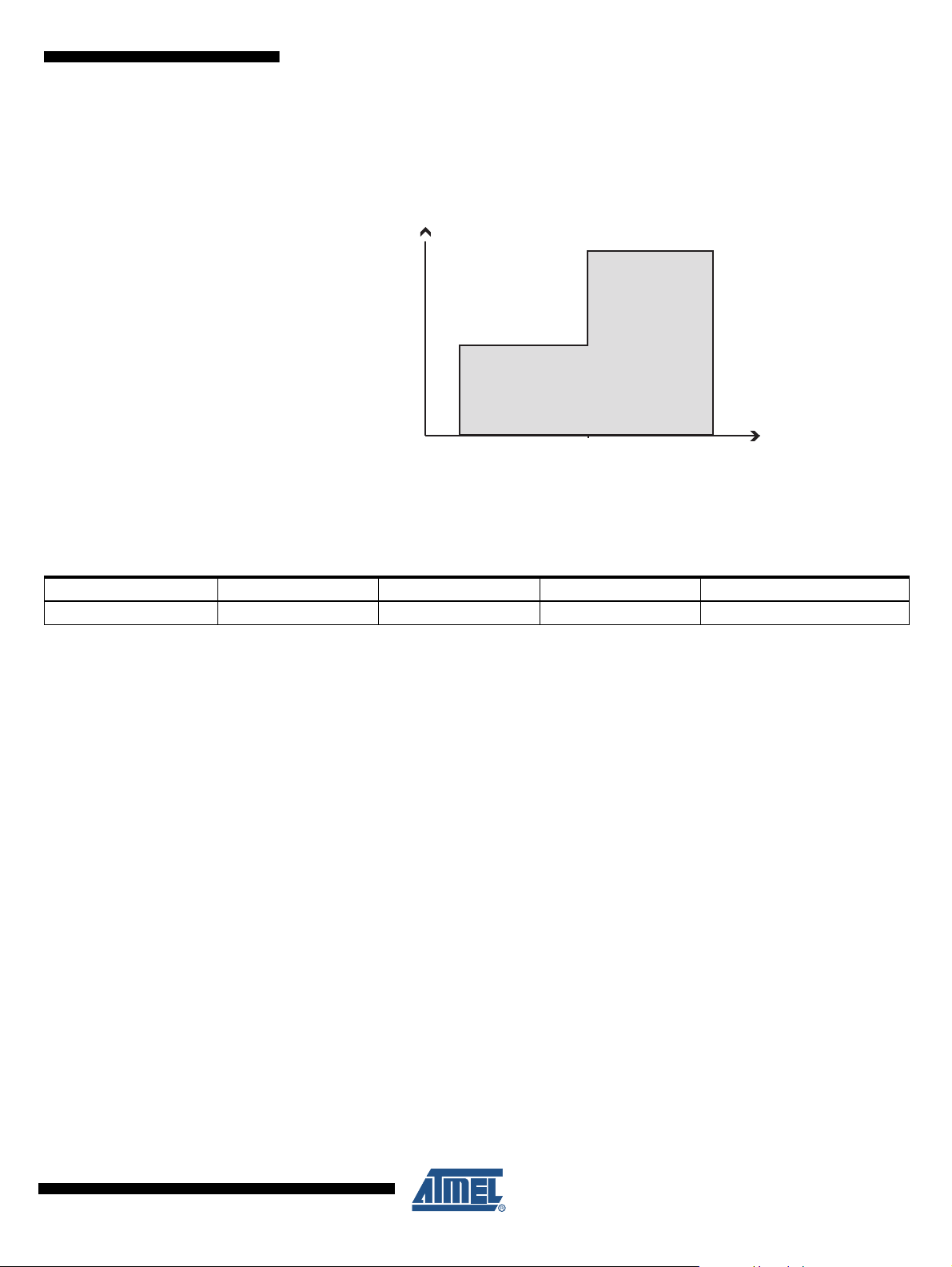
1.3 Maximum Speed versus V
Maximum frequency is dependent on V
V
curve is linear between 1.8V < VCC < 3.6V.
CC
Figure 1-1. Maximum Frequency versus V
CC
As shown in Figure 1-1, the Maximum Frequency vs.
CC.
CC
1.4 Clock Characterizations
Table 1-1. Calibration Accuracy of Internal RC Oscillator
Frequency V
User Calibration 7.3 MHz to 8.1 MHz 1.8V to 3.6V –40°C to +85°C ±25%
CC
Temperature Accuracy
7819A–AVR–01/09
3

1.5 ADC Characteristics
TA = –40° C to +85°C, VCC = 1.8V to 3.6V (unless otherwise noted)
Symbol Parameters Test Conditions Min. Typ. Max. Unit
Resolution Single ended conversion 10 Bits
Absolute accuracy (Including INL,
DNL, quantization error, gain and
offset error)
= 1.8V, V
V
CC
ADC clock = 200 kHz
= 1.8V, V
V
CC
ADC clock = 200 kHz
= 1.8V,
Ref
= 1.8V,
Ref
24.0LSB
24.0LSB
Noise Reduction Mode
= 1.8V, V
V
Integral Non-Linearity (INL)
Differential Non-Linearity (DNL)
Gain error
Offset error
V
REF
Reference voltage 1.8 AV
CC
ADC clock = 200 kHz
= 1.8V, V
V
CC
ADC clock = 200 kHz
= 1.8V, V
V
CC
ADC clock = 200 kHz
= 1.8V, V
V
CC
ADC clock = 200 kHz
= 1.8V,
Ref
= 1.8V,
Ref
= 1.8V,
Ref
= 1.8V,
Ref
0.5 1.5 LSB
0.2 0.7 LSB
–7.0 –3.0 +5.0 LSB
–3.5 +1.5 +3.5 LSB
CC
1.6 ADC Characteristics
TA = –40° C to +85°C, VCC = 1.8V to 3.6V (unless otherwise noted)
Symbol Parameters Test Conditions Min. Typ. Max. Unit
Resolution
Absolute accuracy (Including INL,
DNL, quantization error, gain and
offset error)
Integral Non-Linearity (INL)
Differential Non-Linearity (DNL)
Gain Error
Offset Error
V
REF
Reference Voltage 1.30
Differential conversion, gain = 1x
BIPOLAR mode only
Gain = 1x, V
= 1.8V, V
CC
Ref
=1.3V,
ADC clock = 125 kHz
Gain = 1x, VCC = 1.8V,
= 1.3V,
V
Ref
ADC clock = 125kHz
Gain = 1x, V
= 1.3V,
V
Ref
= 1.8V,
CC
ADC clock = 125 kHz
Gain = 1x, V
V
= 1.3V,
Ref
= 1.8V,
CC
ADC clock = 125 kHz
Gain = 1x, V
= 1.3V,
V
Ref
= 1.8V.
CC
ADC clock = 125 kHz
8Bits
1.6 5.0 LSB
0.7 2.5 LSB
0.3 1.0 LSB
–7.0 +1.50 +7.0 LSB
–4.0 0.0 +4.0 LSB
AVC C –
0.5
V
V
4
ATtiny24V/ATtiny44V/ATtiny84V [Preliminary]
7819A–AVR–01/09

ATtiny24V/ATtiny44V/ATtiny84V [Preliminary]
2. Ordering Information
Power Supply Speed (MHz) ISP Flash Ordering Code Package Operation Range
1.8V to 3.6V 4-8 2 KB ATtiny24V-15SST TU Automotive (–40°C to +85°C)
1.8V to 3.6V 4-8 2 KB ATtiny24V-15MT PN Automotive (–40°C to +85°C)
1.8V to 3.6V 4-8 4 KB ATtiny44V-15SST TU Automotive (–40°C to +85°C)
1.8V to 3.6V 4-8 4 KB ATtiny44V-15MT PN Automotive (–40°C to +85°C)
1.8V to 3.6V 4-8 8 KB ATtiny84V-15MT PN Automotive (–40°C to +85°C)
3. Package Information
Table 3-1. Package Types
Package Type Description
TU
PN
TU 14-Lead, 0.150” Body Width
Plastic Gull Wing Small Outline Package (SOIC)
PN 32-Lead, 5.0 x 5.0 mm Body, 0.50 mm Pitch
Quad Flat No Lead ackage (QFN)
7819A–AVR–01/09
5

Figure 3-1. TU
6
ATtiny24V/ATtiny44V/ATtiny84V [Preliminary]
7819A–AVR–01/09

Figure 3-2. PN
ATtiny24V/ATtiny44V/ATtiny84V [Preliminary]
7819A–AVR–01/09
7

Headquarters International
Atmel Corporation
2325 Orchard Parkway
San Jose, CA 95131
USA
Tel: 1(408) 441-0311
Fax: 1(408) 487-2600
Atmel Asia
Unit 1-5 & 16, 19/F
BEA Tower, Millennium City 5
418 Kwun Tong Road
Kwun Tong, Kowloon
Hong Kong
Tel: (852) 2245-6100
Fax: (852) 2722-1369
Product Contact
Web Site
www.atmel.com
Literature Requests
www.atmel.com/literature
Atmel Europe
Le Krebs
8, Rue Jean-Pierre Timbaud
BP 309
78054
Saint-Quentin-en-Yvelines Cedex
France
Tel: (33) 1-30-60-70-00
Fax: (33) 1-30-60-71-11
Technical Support
avr@atmel.com
Atmel Japan
9F, Tonetsu Shinkawa Bldg.
1-24-8 Shinkawa
Chuo-ku, Tokyo 104-0033
Japan
Tel: (81) 3-3523-3551
Fax: (81) 3-3523-7581
Sales Contact
www.atmel.com/contacts
Disclaimer: The information in this document is provided in connection with Atmel products. No license, express or implied, by estoppel or otherwise, to any
intellectual property right is granted by this document or in connection with the sale of Atmel products. EXCEPT AS SET FORTH IN ATMEL’S TERMS AND CONDI-
TIONS OF SALE LOCATED ON ATMEL’S WEB SITE, ATMEL ASSUMES NO LIABILITY WHATSOEVER AND DISCLAIMS ANY EXPRESS, IMPLIED OR STATUTORY
WARRANTY RELATING TO ITS PRODUCTS INCLUDING, BUT NOT LIMITED TO, THE IMPLIED WARRANTY OF MERCHANTABILITY, FITNESS FOR A PARTICULAR
PURPOSE, OR NON-INFRINGEMENT. IN NO EVENT SHALL ATMEL BE LIABLE FOR ANY DIRECT, INDIRECT, CONSEQUENTIAL, PUNITIVE, SPECIAL OR INCIDENTAL DAMAGES (INCLUDING, WITHOUT LIMITATION, DAMAGES FOR LOSS OF PROFITS, BUSINESS INTERRUPTION, OR LOSS OF INFORMATION) ARISING OUT OF
THE USE OR INABILITY TO USE THIS DOCUMENT, EVEN IF ATMEL HAS BEEN ADVISED OF THE POSSIBILITY OF SUCH DAMAGES. Atmel makes no
representations or warranties with respect to the accuracy or completeness of the contents of this document and reserves the right to make changes to specifications
and product descriptions at any time without notice. Atmel does not make any commitment to update the information contained herein. Unless specifically provided
otherwise, Atmel products are not suitable for, and shall not be used in, automotive applications. Atmel’s products are not intended, authorized, or warranted for use
as components in applications intended to support or sustain life.
© 2009 Atmel Corporation. All rights reserved. Atmel®, logo and combinations thereof, AVR® and others are registered trademarks or trade-
marks of Atmel Corporation or its subsidiaries. Other terms and product names may be trademarks of others.
7819A–AVR–01/09
 Loading...