


Features
• High-performance, Low-power AVR
• RISC Architecture
– 118 Powerful Instructions – Most Single Clock Cycle Execution
– 32 x 8 General Purpose Working Registers
– Fully Static Operation
– Up to 16 MIPS Throughput at 16 MHz
• Data and Non-volatile Program Memory
– 2K Bytes of In-System Programmable Program Memory Flash
Endurance: 10,000 Write/Erase Cycles
– 128 Bytes of In-System Programmable EEPROM
Endurance: 100,000 Write/Erase Cycles
– 128 Bytes Internal SRAM
– Programming Lock for Flash Program and EEPROM Data Security
• Peripheral Features
– 8-bit Timer/Counter with Separate Prescaler
– 8-bit High-speed Timer with Separate Prescaler
2 High Frequency PWM Outputs with Separate Output Compare Registers
Non-overlapping Inverted PWM Output Pins
– Universal Serial Interface with Start Condition Detector
– 10-bit ADC
11 Single Ended Channels
8 Differential ADC Channels
7 Differential ADC Channel Pairs with Programmable Gain (1x, 20x)
– On-chip Analog Comparator
– External Interrupt
– Pin Change Interrupt on 11 Pins
– Programmable Watchdog Timer with Separate On-chip Oscillator
• Special Microcontroller Features
– Low Power Idle, Noise Reduction, and Power-down Modes
– Power-on Reset and Programmable Brown-out Detection
– External and Internal Interrupt Sources
– In-System Programmable via SPI Port
– Internal Calibrated RC Oscillator
• I/O and Packages
– 20-lead PDIP/SOIC: 16 Programmable I/O Lines
– 32-lead QFN/MLF: 16 programmable I/O Lines
• Operating Voltages
– 2.7V - 5.5V for ATtiny26L
– 4.5V - 5.5V for ATtiny26
• Speed Grades
– 0 - 8 MHz for ATtiny26L
– 0 - 16 MHz for ATtiny26
• Power Consumption at 1 MHz, 3V and 25°C for ATtiny26L
– Active 16 MHz, 5V and 25°C: Typ 15 mA
– Active 1 MHz, 3V and 25°C: 0.70 mA
– Idle Mode 1 MHz, 3V and 25°C: 0.18 mA
– Power-down Mode: < 1 µA
®
8-bit Microcontroller
8-bit
Microcontroller
with 2K Bytes
Flash
ATtiny26
ATtiny26L
1477F–AVR–12/04
Rev. 1477F–AVR–12/04
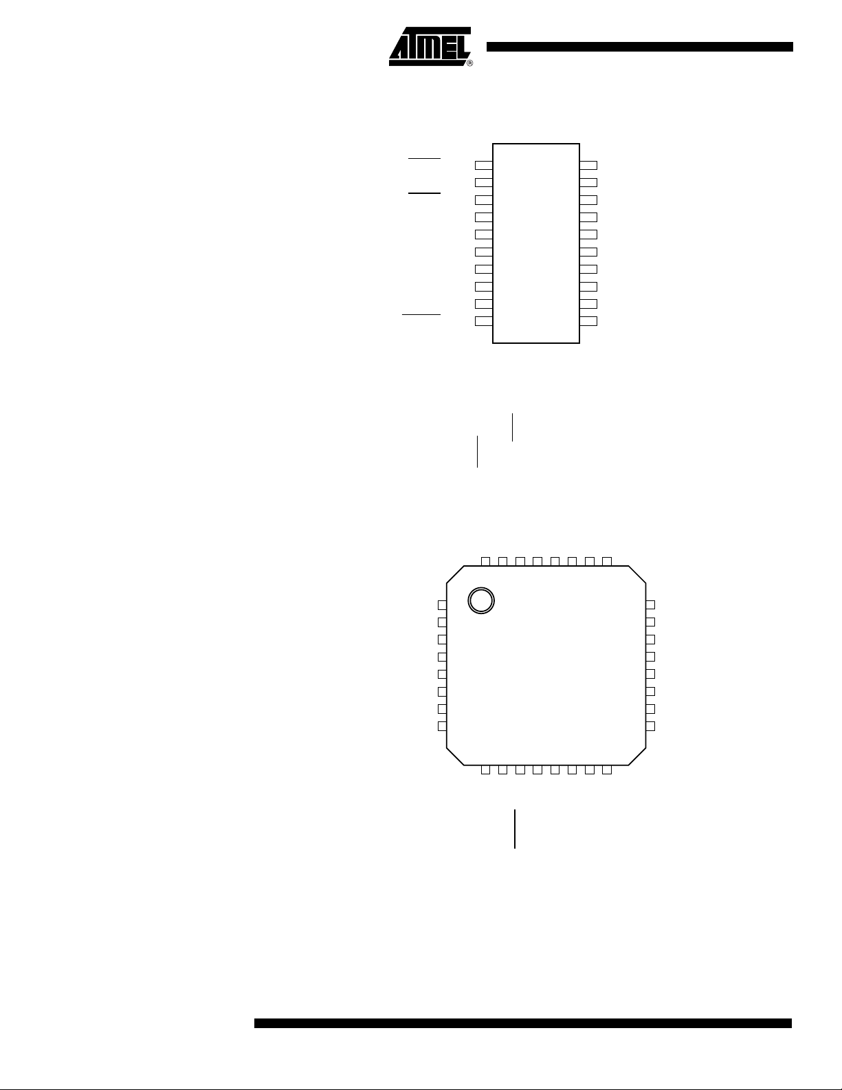
Pin Configuration
PDIP/SOIC
(MOSI/DI/SDA/OC1A) PB0
(MISO/DO/OC1A) PB1
(SCK/SCL/OC1B) PB2
(OC1B) PB3
VCC
GND
(ADC7/XTAL1) PB4
(ADC8/XTAL2) PB5
(ADC9/INT0/T0) PB6
(ADC10/RESET) PB7
1
2
3
4
5
6
7
8
9
10
20
19
18
17
16
15
14
13
12
11
MLF Top View
PB2 (SCK/SCL/OC1B)
PB1 (MISO/DO/OC1A)
PB0 (MOSI/DI/SDA/OC1A)
NCNCNC
PA0 (ADC0)
PA0 (ADC0)
PA1 (ADC1)
PA2 (ADC2)
PA3 (AREF)
GND
AVCC
PA4 (ADC3)
PA5 (ADC4)
PA6 (ADC5/AIN0)
PA7 (ADC6/AIN1)
PA1 (ADC1)
NC
(OC1B) PB3
NC
VCC
GND
NC
(ADC7/XTAL1) PB4
(ADC8/XTAL2) PB5
32313029282726
1
2
3
4
5
6
7
8
9
10111213141516
NC
(ADC9/INT0/T0) PB6
NC
(ADC6/AIN1) PA7
(ADC10/RESET) PB7
25
NC
24
PA2 (ADC2)
23
PA3 (AREF)
22
GND
21
NC
20
NC
19
AVCC
18
PA4 (ADC3)
17
NC
(ADC4) PA5
(ADC5/AIN0) PA6
Note: Note: The bottom pad under the QFN/MLF package should be soldered to ground.
2
ATtiny26(L)
1477F–AVR–12/04

ATtiny26(L)
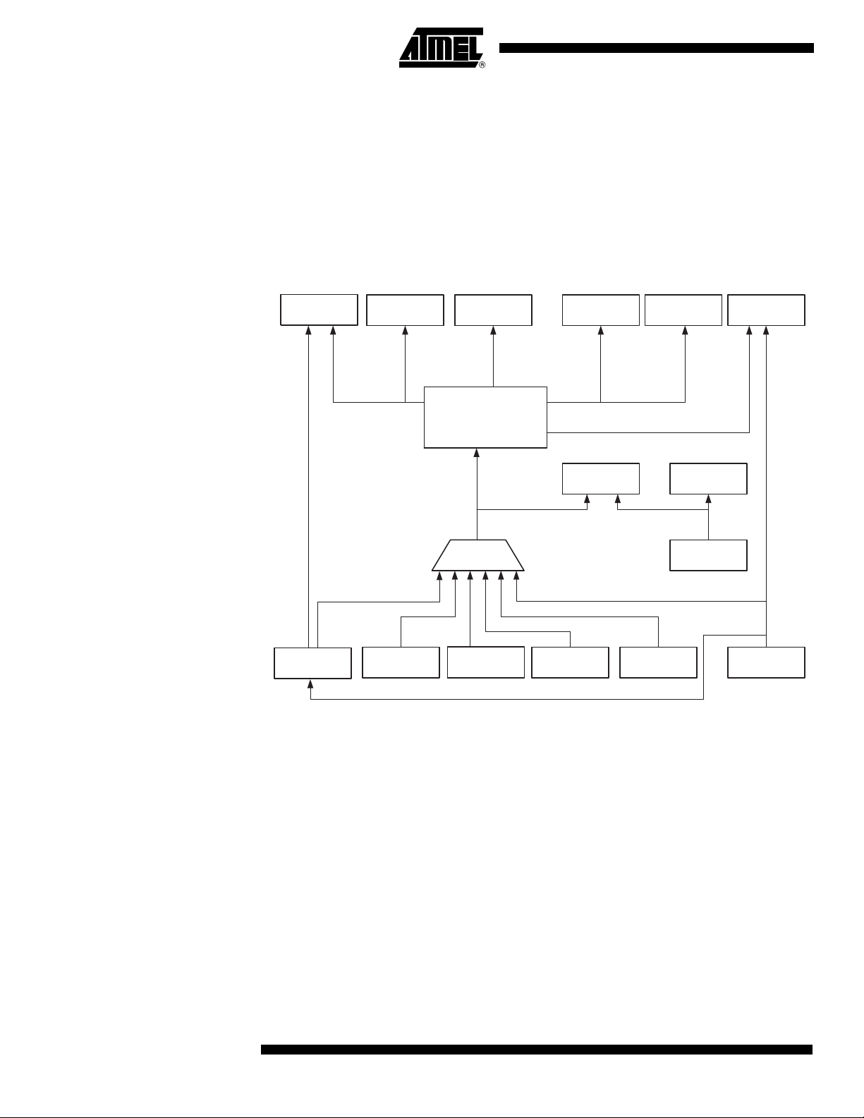
Description The ATtiny26(L) is a low-power CMOS 8-bit microcontroller based on the AVR
enhanced RISC architecture. By executing powerful instructions in a single clock cycle,
the ATtiny26(L) achieves throughputs approaching 1 MIPS per MHz allowing the system
designer to optimize power consumption versus processing speed.
The AVR core combines a rich instruction set with 32 general purpose working registers.
All the 32 registers are directly connected to the Arithmetic Logic Unit (ALU), allowing
two independent registers to be accessed in one single instruction executed in one clock
cycle. The resulting architecture is more code efficient while achieving throughputs up to
ten times faster than conventional CISC microcontrollers. The ATtiny26(L) has a high
precision ADC with up to 11 single ended channels and 8 differential channels. Seven
differential channels have an optional gain of 20x. Four out of the seven differential
channels, which have the optional gain, can be used at the same time. The ATtiny26(L)
also has a high frequency 8-bit PWM module with two independent outputs. Two of the
PWM outputs have inverted non-overlapping output pins ideal for synchronous rectification. The Universal Serial Interface of the ATtiny26(L) allows efficient software
implementation of TWI (Two-wire Serial Interface) or SM-bus interface. These features
allow for highly integrated battery charger and lighting ballast applications, low-end thermostats, and firedetectors, among other applications.
The ATtiny26(L) provides 2K bytes of Flash, 128 bytes EEPROM, 128 bytes SRAM, up
to 16 general purpose I/O lines, 32 general purpose working registers, two 8-bit
Timer/Counters, one with PWM outputs, internal and external Oscillators, internal and
external interrupts, programmable Watchdog Timer, 11-channel, 10-bit Analog to Digital
Converter with two differential voltage input gain stages, and four software selectable
power saving modes. The Idle mode stops the CPU while allowing the Timer/Counters
and interrupt system to continue functioning. The ATtiny26(L) also has a dedicated ADC
Noise Reduction mode for reducing the noise in ADC conversion. In this sleep mode,
only the ADC is functioning. The Power-down mode saves the register contents but
freezes the oscillators, disabling all other chip functions until the next interrupt or hardware reset. The Standby mode is the same as the Power-down mode, but external
oscillators are enabled. The wakeup or interrupt on pin change features enable the
ATtiny26(L) to be highly responsive to external events, still featuring the lowest power
consumption while in the Power-down mode.
1477F–AVR–12/04
The device is manufactured using Atmel’s high density non-volatile memory technology.
By combining an enhanced RISC 8-bit CPU with Flash on a monolithic chip, the
ATtiny26(L) is a powerful microcontroller that provides a highly flexible and cost effective solution to many embedded control applications.
The ATtiny26(L) AVR is supported with a full suite of program and system development
tools including: Macro assemblers, program debugger/simulators, In-circuit emulators,
and evaluation kits.
3
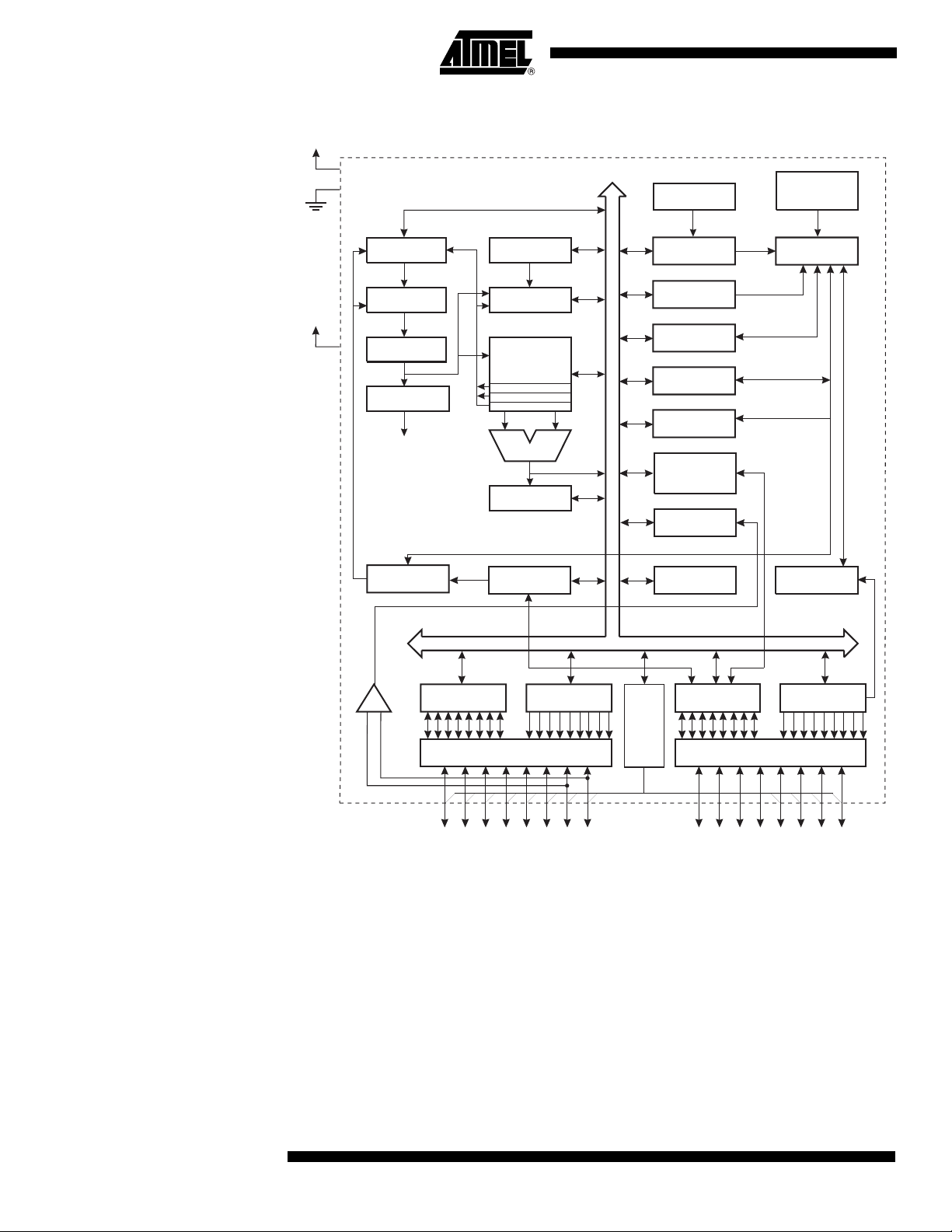
Block Diagram Figure 1. The ATtiny26(L) Block Diagram
VCC
GND
AVCC
PROGRAM
COUNTER
PROGRAM
FLASH
INSTRUCTION
REGISTER
INSTRUCTION
DECODER
CONTROL
LINES
PROGRAMMING
LOGIC
STACK
POINTER
SRAM
GENERAL
PURPOSE
REGISTERS
X
Y
Z
ALU
STATUS
REGISTER
ISP INTERFACE
8-BIT DATA BUS
INTERNAL
OSCILLATOR
WATCHDOG
TIMER
MCU CONTROL
REGISTER
MCU STATUS
REGISTER
TIMER/
COUNTER0
TIMER/
COUNTER1
UNIVERSAL
SERIAL
INTERFACE
INTERRUPT
UNIT
EEPROM
INTERNAL
CALIBRATED
OSCILLATOR
TIMING AND
CONTROL
OSCILLATORS
+
-
DATA REGISTER
PORT A
ANALOG
COMPARATOR
DATA DIR.
REG.PORT A
PORT A DRIVERS
PA0-PA7
ADC
DATA REGISTER
PORT B
PORT B DRIVERS
PB0-PB7
DATA DIR.
REG.PORT B
4
ATtiny26(L)
1477F–AVR–12/04

ATtiny26(L)
Pin Descriptions
VCC Digital supply voltage pin.
GND Digital ground pin.
AVCC AVCC is the supply voltage pin for Port A and the A/D Converter (ADC). It should be
externally connected to V
connected to V
ADC.
Port A (PA7..PA0) Port A is an 8-bit general purpose I/O port. PA7..PA0 are all I/O pins that can provide
internal pull-ups (selected for each bit). Port A has alternate functions as analog inputs
for the ADC and analog comparator and pin change interrupt as described in “Alternate
Port Functions” on page 46.
Port B (PB7..PB0) Port B is an 8-bit general purpose I/O port. PB6..0 are all I/O pins that can provide inter-
nal pull-ups (selected for each bit). PB7 is an I/O pin if not used as the reset. To use pin
PB7 as an I/O pin, instead of RESET pin, program (“0”) RSTDISBL Fuse. Port B has
alternate functions for the ADC, clocking, timer counters, USI, SPI programming, and
pin change interrupt as described in “Alternate Port Functions” on page 46.
through a low-pass filter. See page 94 for details on operating of the
CC
, even if the ADC is not used. If the ADC is used, it should be
CC
An External Reset is generated by a low level on the PB7/RESET
longer than 50 ns will generate a reset, even if the clock is not running. Shorter pulses
are not guaranteed to generate a reset.
XTAL1 Input to the inverting oscillator amplifier and input to the internal clock operating circuit.
XTAL2 Output from the inverting oscillator amplifier.
About Code Examples
This datasheet contains simple code examples that briefly show how to use various
parts of the device. These code examples assume that the part specific header file is
included before compilation. Be aware that not all C compiler vendors include bit definitions in the header files and interrupt handling in C is compiler dependent. Please
confirm with the C compiler documentation for more details.
pin. Reset pulses
1477F–AVR–12/04
5
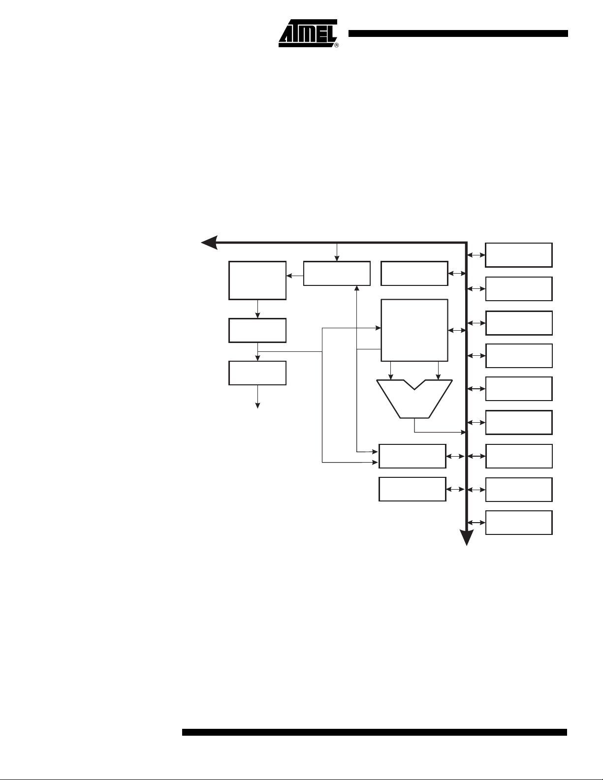
AVR CPU Core
Architectural Overview The fast-access Register File concept contains 32 x 8-bit general purpose working reg-
isters with a single clock cycle access time. This means that during one single clock
cycle, one ALU (Arithmetic Logic Unit) operation is executed. Two operands are output
from the Register File, the operation is executed, and the result is stored back in the
Register File – in one clock cycle.
Six of the 32 registers can be used as 16-bit pointers for indirect memory access. These
pointers are called the X-, Y-, and Z-pointers, and they can address the Register File
and the Flash program memory.
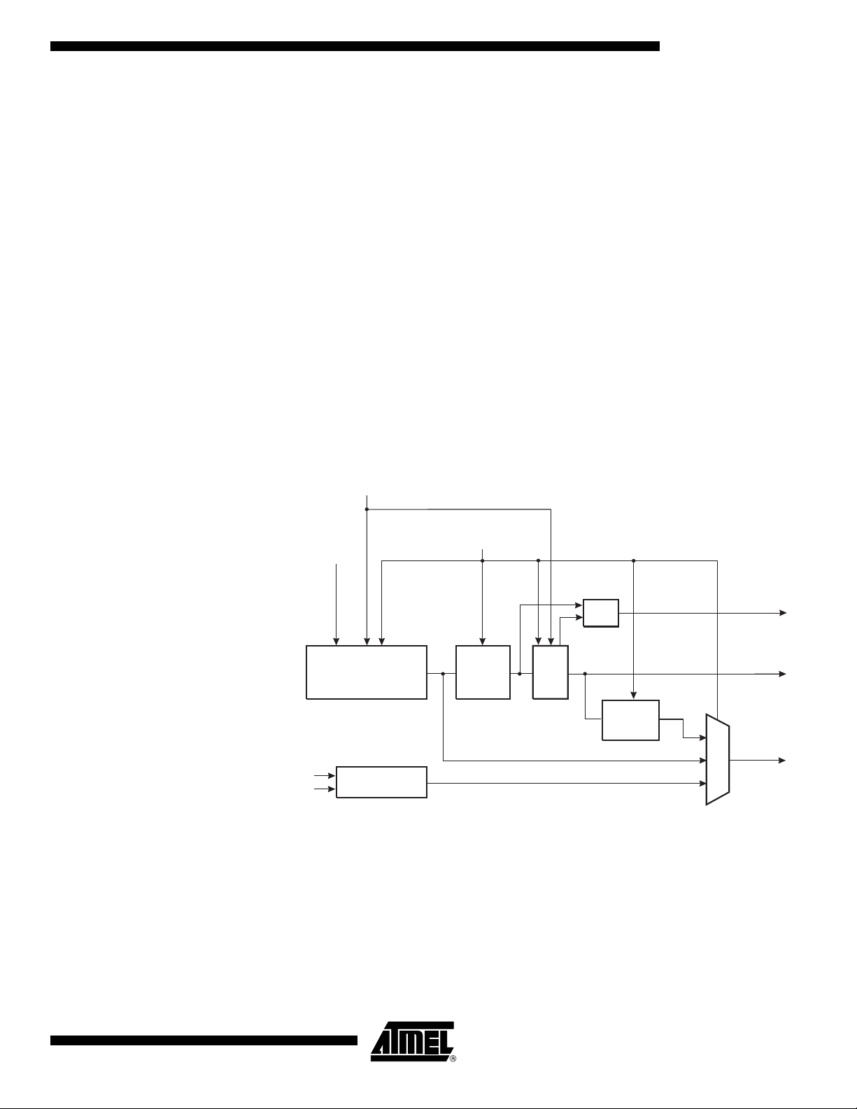
Figure 2. The ATtiny26(L) AVR Enhanced RISC Architecture
8-bit Data Bus
Control
Registers
Interrupt
Unit
1024 x 16
Program
FLASH
Program
Counter
Status
and Test
Instruction
Register
Instruction
Decoder
Control Lines
Direct Addressing
Indirect Addressing
32 x 8
General
Purpose
Registers
ALU
128 x 8
SRAM
128 byte
EEPROM
Universal
Serial Interface
ISP Unit
2 x 8-bit
Timer/Counter
Watchdog
Timer
ADC
Analog
Comparator
I/O Lines
The ALU supports arithmetic and logic functions between registers or between a constant and a register. Single register operations are also executed in the ALU. Figure 2
shows the ATtiny26(L) AVR Enhanced RISC microcontroller architecture. In addition to
the register operation, the conventional memory addressing modes can be used on the
Register File as well. This is enabled by the fact that the Register File is assigned the 32
lowermost Data Space addresses ($00 - $1F), allowing them to be accessed as though
they were ordinary memory locations.
The I/O memory space contains 64 addresses for CPU peripheral functions as Control
Registers, Timer/Counters, A/D Converters, and other I/O functions. The I/O Memory
can be accessed directly, or as the Data Space locations following those of the Register
File, $20 - $5F.
6
ATtiny26(L)
1477F–AVR–12/04

ATtiny26(L)
The AVR uses a Harvard architecture concept with separate memories and buses for
program and data memories. The program memory is accessed with a two stage
pipelining. While one instruction is being executed, the next instruction is pre-fetched
from the program memory. This concept enables instructions to be executed in every
clock cycle. The program memory is In-System programmable Flash memory.
With the relative jump and relative call instructions, the whole address space is directly
accessed. All AVR instructions have a single 16-bit word format, meaning that every
program memory address contains a single 16-bit instruction.
During interrupts and subroutine calls, the return address program counter (PC) is
stored on the Stack. The Stack is effectively allocated in the general data SRAM, and
consequently the stack size is only limited by the total SRAM size and the usage of the
SRAM. All user programs must initialize the SP in the reset routine (before subroutines
or interrupts are executed). The 8-bit Stack Pointer SP is read/write accessible in the I/O
space. For programs written in C, the stack size must be declared in the linker file. Refer
to the C user guide for more information.
The 128 bytes data SRAM can be easily accessed through the five different addressing
modes supported in the AVR architecture.
The memory spaces in the AVR architecture are all linear and regular memory maps.
The I/O memory space contains 64 addresses for CPU peripheral functions as Control
Registers, Timer/Counters, and other I/O functions. The memory spaces in the AVR
architecture are all linear and regular memory maps.
General Purpose Register File
A flexible interrupt module has its control registers in the I/O space with an additional
Global Interrupt Enable bit in the Status Register. All the different interrupts have a separate Interrupt Vector in the Interrupt Vector table at the beginning of the program
memory. The different interrupts have priority in accordance with their Interrupt Vector
position. The lower the Interrupt Vector address, the higher the priority.
Figure 3 shows the structure of the 32 general purpose working registers in the CPU.
Figure 3. AVR CPU General Purpose Working Registers
7 0 Addr.
R0 $00
R1 $01
R2 $02
…
R13 $0D
General R14 $0E
Purpose R15 $0F
Working R16 $10
Registers R17 $11
…
R26 $1A X-register Low Byte
R27 $1B X-register High Byte
R28 $1C Y-register Low Byte
R29 $1D Y-register High Byte
R30 $1E Z-register Low Byte
R31 $1F Z-register High Byte
1477F–AVR–12/04
7

All of the register operating instructions in the instruction set have direct and single cycle
access to all registers. The only exceptions are the five constant arithmetic and logic
instructions SBCI, SUBI, CPI, ANDI, and ORI between a constant and a register, and
the LDI instruction for load immediate constant data. These instructions apply to the
second half of the registers in the Register File – R16..R31. The general SBC, SUB, CP,
AND, and OR, and all other operations between two registers or on a single register
apply to the entire Register File.
As shown in Figure 3, each register is also assigned a data memory address, mapping
them directly into the first 32 locations of the user Data Space. Although not being physically implemented as SRAM locations, this memory organization provides flexibility in
access of the registers, as the X-, Y-, and Z-registers can be set to index any register in
the file.
X-register, Y-register, and Zregister
ALU – Arithmetic Logic
Unit
The registers R26..R31 have some added functions to their general purpose usage.
These registers are address pointers for indirect addressing of the Data Space. The
three indirect address registers X, Y, and Z are defined as:
Figure 4. X-, Y-, and Z-register
15 0
X-register 7 0 7 0
R27 ($1B) R26 ($1A)
15 0
Y-register 7 0 7 0
R29 ($1D) R28 ($1C)
15 0
Z-register 7 0 7 0
R31 ($1F) R30 ($1E)
In the different addressing modes, these address registers have functions as fixed displacement, automatic increment and decrement (see the descriptions for the different
instructions).
The high-performance AVR ALU operates in direct connection with all 32 general purpose working registers. Within a single clock cycle, ALU operations between registers in
the Register File are executed. The ALU operations are divided into three main categories – Arithmetic, Logical, and Bit-functions.
8
ATtiny26(L)
1477F–AVR–12/04

ATtiny26(L)
Status Register – SREG The AVR Status Register – SREG – at I/O space location $3F is defined as:
Bit 76543210
$3F ($5F) I T H S V N Z C SREG
Read/Write R/W R/W R/W R/W R/W R/W R/W R/W
Initial Value 0 0 0 0 0 0 0 0
• Bit 7 – I: Global Interrupt Enable
The Global Interrupt Enable bit must be set (one) for the interrupts to be enabled. The
individual interrupt enable control is then performed in the Interrupt Mask Registers –
GIMSK and TIMSK. If the Global Interrupt Enable Register is cleared (zero), none of the
interrupts are enabled independent of the GIMSK and TIMSK values. The I-bit is cleared
by hardware after an interrupt has occurred, and is set by the RETI instruction to enable
subsequent interrupts. The I-bit can also be set and cleared by the application with the
SEI and CLI instructions, as described in the instruction set reference.
• Bit 6 – T: Bit Copy Storage
The Bit Copy instructions BLD (Bit LoaD) and BST (Bit STore) use the T-bit as source
and destination for the operated bit. A bit from a register in the Register File can be copied into T by the BST instruction, and a bit in T can be copied into a bit in a register in the
Register File by the BLD instruction.
• Bit 5 – H: Half Carry Flag
The Half Carry Flag H indicates a Half Carry in some arithmetic operations. See the
Instruction Set Description for detailed information.
• Bit 4 – S: Sign Bit, S = N ⊕ V
The S-bit is always an exclusive or between the Negative Flag N and the Two’s Complement Overflow Flag V. See the Instruction Set Description for detailed information.
• Bit 3 – V: Two’s Complement Overflow Flag
The Two’s Complement Overflow Flag V supports two’s complement arithmetics. See
the Instruction Set Description for detailed information.
• Bit 2 – N: Negative Flag
The Negative Flag N indicates a negative result after the different arithmetic and logic
operations. See the Instruction Set Description for detailed information.
• Bit 1 – Z: Zero Flag
The Zero Flag Z indicates a zero result after the different arithmetic and logic operations. See the Instruction Set Description for detailed information.
• Bit 0 – C: Carry Flag
The Carry Flag C indicates a carry in an arithmetic or logic operation. See the Instruction
Set Description for detailed information.
1477F–AVR–12/04
9
Stack Pointer – SP The ATtiny26(L) Stack Pointer is implemented as an 8-bit register in the I/O space loca-
tion $3D ($5D). As the ATtiny26(L) data memory has 224 ($E0) locations, eight bits are
used.
Bit 76543210
$3D ($5D) SP7 SP6 SP5 SP4 SP3 SP2 SP1 SP0 SP
Read/Write R/W R/W R/W R/W R/W R/W R/W R/W
Initial Value 0 0 0 0 0 0 0 0
The Stack Pointer points to the data SRAM stack area where the Subroutine and Interrupt Stacks are located. This Stack space in the data SRAM must be defined by the
program before any subroutine calls are executed or interrupts are enabled. The Stack
Pointer must be set to point above $60. The Stack Pointer is decremented by one when
data is pushed onto the Stack with the PUSH instruction, and it is decremented by two
when an address is pushed onto the Stack with subroutine calls and interrupts. The
Stack Pointer is incremented by one when data is popped from the Stack with the POP
instruction, and it is incremented by two when an address is popped from the Stack with
return from subroutine RET or return from interrupt RETI.
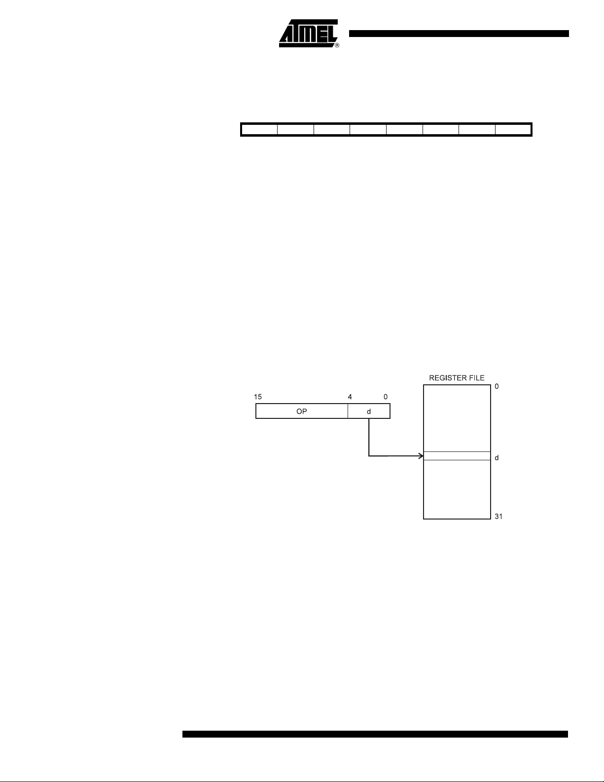
Program and Data Addressing Modes
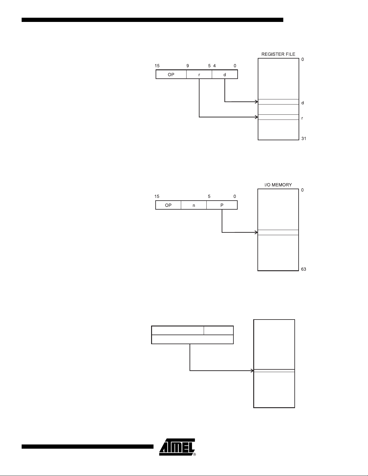
Register Direct, Single Register Rd
The ATtiny26(L) AVR Enhanced RISC microcontroller supports powerful and efficient
addressing modes for access to the Flash program memory, SRAM, Register File, and
I/O Data memory. This section describes the different addressing modes supported by
the AVR architecture. In the figures, OP means the operation code part of the instruction
word. To simplify, not all figures show the exact location of the addressing bits.
Figure 5. Direct Single Register Addressing
The operand is contained in register d (Rd).
10
ATtiny26(L)
1477F–AVR–12/04
ATtiny26(L)
Register Direct, Two Registers
Figure 6. Direct Register Addressing, Two Registers
Rd and Rr
Operands are contained in register r (Rr) and d (Rd). The result is stored in register d
(Rd).
I/O Direct Figure 7. I/O Direct Addressing
Operand address is contained in 6 bits of the instruction word. n is the destination or
source register address.
Data Direct Figure 8. Direct Data Addressing
31
OP Rr/Rd
15 0
1477F–AVR–12/04
20 19
16 LSBs
16
Data Space
$0000
$00DF
11
A 16-bit Data Address is contained in the 16 LSBs of a two-word instruction. Rd/Rr
specify the destination or source register.
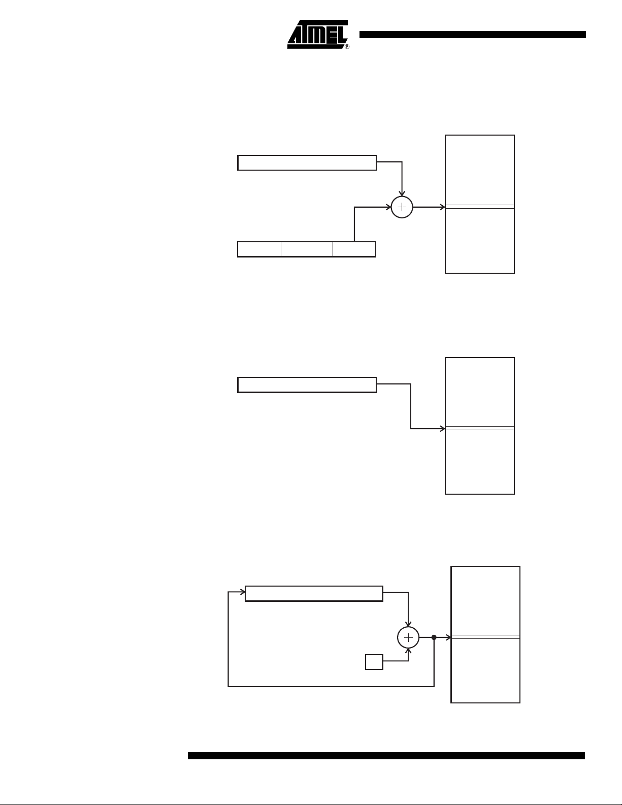
Data Indirect with
Figure 9. Data Indirect with Displacement
Displacement
15
Y OR Z - REGISTER
15
OP an
Operand address is the result of the Y- or Z-register contents added to the address contained in 6 bits of the instruction word.
Data Indirect Figure 10. Data Indirect Addressing
X-, Y-, OR Z-REGISTER
Data Space
$0000
0
05610
$00DF
Data Space
$0000
015
Data Indirect with Predecrement
12
ATtiny26(L)
$00DF
Operand address is the contents of the X-, Y-, or the Z-register.
Figure 11. Data Indirect Addressing with Pre-decrement
Data Space
$0000
015
X-, Y-, OR Z-REGISTER
-1
$00DF
1477F–AVR–12/04
ATtiny26(L)
The X-, Y-, or Z-register is decremented before the operation. Operand address is the
decremented contents of the X-, Y-, or Z-register.
Data Indirect with Postincrement
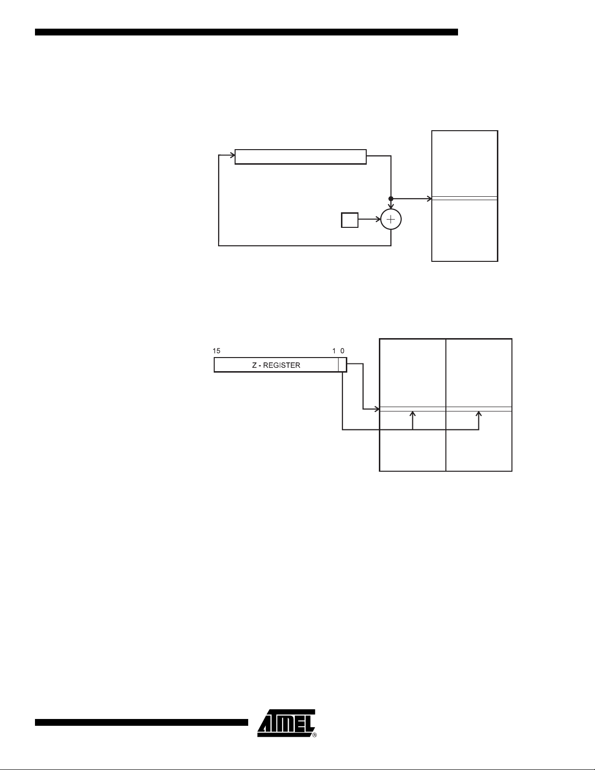
Constant Addressing Using the LPM Instruction
Figure 12. Data Indirect Addressing with Post-increment
Data Space
015
X-, Y-, OR Z-REGISTER
1
$0000
$00DF
The X-, Y-, or Z-register is incremented after the operation. Operand address is the content of the X-, Y-, or Z-register prior to incrementing.
Figure 13. Code Memory Constant Addressing
PROGRAM MEMORY
$000
1477F–AVR–12/04
$3FF
Constant byte address is specified by the Z-register contents. The 15 MSBs select word
address (0 - 1K), the LSB selects low byte if cleared (LSB = 0) or high byte if set
(LSB = 1).
13

Indirect Program Addressing, IJMP and ICALL
Figure 14. Indirect Program Memory Addressing
PROGRAM MEMORY
$000
$3FF
Program execution continues at address contained by the Z-register (i.e., the PC is
loaded with the contents of the Z-register).
Relative Program Addressing, RJMP and RCALL
Figure 15. Relative Program Memory Addressing
PROGRAM MEMORY
+1
$000
$3FF
Program execution continues at address PC + k + 1. The relative address k is from
-2048 to 2047.
14
ATtiny26(L)
1477F–AVR–12/04
ATtiny26(L)
Memories The AVR CPU is driven by the System Clock Ø, directly generated from the external
clock crystal for the chip. No internal clock division is used.
Figure 16 shows the parallel instruction fetches and instruction executions enabled by
the Harvard architecture and the fast-access Register File concept. This is the basic
pipelining concept to obtain up to 1 MIPS per MHz with the corresponding unique results
for functions per cost, functions per clocks, and functions per power-unit.
Figure 16. The Parallel Instruction Fetches and Instruction Executions
T1 T2 T3 T4
System Clock Ø
1st Instruction Fetch
1st Instruction Execute
2nd Instruction Fetch
2nd Instruction Execute
3rd Instruction Fetch
3rd Instruction Execute
4th Instruction Fetch
Figure 17 shows the internal timing concept for the Register File. In a single clock cycle
an ALU operation using two register operands is executed, and the result is stored back
to the destination register.
Figure 17. Single Cycle ALU Operation
T1 T2 T3 T4
System Clock Ø
Total Execution Time
Register Operands Fetch
ALU Operation Execute
Result Write Back
The internal data SRAM access is performed in two System Clock cycles as described
in Figure 18.
1477F–AVR–12/04
15
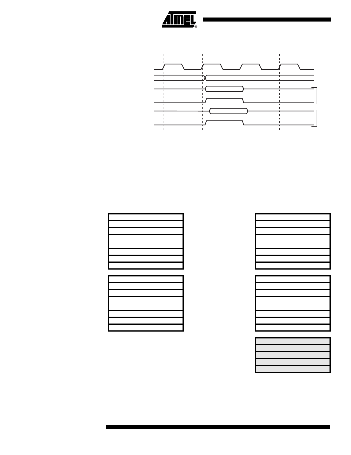
Figure 18. On-chip Data SRAM Access Cycles
T1 T2 T3 T4
System Clock Ø
In-System Programmable Flash Program Memory
Address
Prev. Address
Address
Data
WR
Write
Data
RD
Read
The ATtiny26(L) contains 2K bytes On-chip In-System Programmable Flash memory for
program storage. Since all instructions are 16- or 32-bit words, the Flash is organized as
1K x 16. The Flash memory has an endurance of at least 10,000 write/erase cycles. The
ATtiny26(L) Program Counter – PC – is 10 bits wide, thus addressing the 1024 program
memory addresses, see “Memory Programming” on page 107 for a detailed description
on Flash data downloading. See “Program and Data Addressing Modes” on page 10 for
the different program memory addressing modes.
Figure 19. SRAM Organization
Register File Data Address Space
R0 $0000
R1 $0001
R2 $0002
... ...
R29 $001D
R30 $001E
R31 $001F
I/O Registers
$00 $0020
$01 $0021
$02 $0022
… …
$3D $005D
$3E $005E
$3F $005F
Internal SRAM
$0060
$0061
$00DE
$00DF
SRAM Data Memory Figure 19 above shows how the ATtiny26(L) SRAM Memory is organized.
The lower 224 Data Memory locations address the Register File, the I/O Memory and
the internal data SRAM. The first 96 locations address the Register File and I/O Memory, and the next 128 locations address the internal data SRAM.
...
16
ATtiny26(L)
1477F–AVR–12/04

ATtiny26(L)
The five different addressing modes for the data memory cover: Direct, Indirect with Displacement, Indirect, Indirect with Pre-decrement, and Indirect with Post-increment. In
the Register File, registers R26 to R31 feature the indirect addressing pointer registers.
The direct addressing reaches the entire data space. The Indirect with Displacement
mode features a 63 address locations reach from the base address given by the Y- or Zregister.
When using register indirect addressing modes with automatic pre-decrement and postincrement, the address registers X, Y, and Z are decremented and incremented.
The 32 general purpose working registers, 64 I/O Registers and the 128 bytes of internal data SRAM in the ATtiny26(L) are all accessible through all these addressing
modes.
See “Program and Data Addressing Modes” on page 10 for a detailed description of the
different addressing modes.
EEPROM Data Memory The ATtiny26(L) contains 128 bytes of data EEPROM memory. It is organized as a sep-
arate data space, in which single bytes can be read and written (see “Memory
Programming” on page 107). The EEPROM has an endurance of at least 100,000
write/erase cycles per location.
EEPROM Read/Write Access The EEPROM Access Registers are accessible in the I/O space.
The write access time is typically 8.3 ms. A self-timing function lets the user software
detect when the next byte can be written. A special EEPROM Ready Interrupt can be
set to trigger when the EEPROM is ready to accept new data.
An ongoing EEPROM write operation will complete even if a reset condition occurs.
In order to prevent unintentional EEPROM writes, a two state write procedure must be
followed. Refer to the description of the EEPROM Control Register for details on this.
When the EEPROM is written, the CPU is halted for two clock cycles before the next
instruction is executed.
When the EEPROM is read, the CPU is halted for four clock cycles before the next
instruction is executed.
EEPROM Address Register –
EEAR
Bit 76543210
$1E ($3E) – EEAR6 EEAR5 EEAR4 EEAR3 EEAR2 EEAR1 EEAR0 EEAR
Read/Write R R/W R/W R/W R/W R/W R/W R/W
Initial Value0XXXXXXX
• Bit 7 – RES: Reserved Bits
This bit are reserved bit in the ATtiny26(L) and will always read as zero.
• Bit 6..0 – EEAR6..0: EEPROM Address
The EEPROM Address Register – EEAR – specifies the EEPROM address in the 128
bytes EEPROM space. The EEPROM data bytes are addressed linearly between 0 and
127. The initial value of EEAR is undefined. A proper value must be written before the
EEPROM may be accessed.
1477F–AVR–12/04
17

EEPROM Data Register –
EEDR
Bit 76543210
$1D ($3D) MSB LSB EEDR
Read/Write R/W R/W R/W R/W R/W R/W R/W R/W
Initial Value00000000
• Bit 7..0 – EEDR7..0: EEPROM Data
For the EEPROM write operation, the EEDR Register contains the data to be written to
the EEPROM in the address given by the EEAR Register. For the EEPROM read operation, the EEDR contains the data read out from the EEPROM at the address given by
EEAR.
EEPROM Control Register –
EECR
Bit 76543210
$1C ($3C) ––––EERIEEEMWEEEWEEEREEECR
Read/WriteRRRRR/WR/WR/WR/W
Initial Value00000000
• Bit 7..4 – RES: Reserved Bits
These bits are reserved bits in the ATtiny26(L) and will always read as zero.
• Bit 3 – EERIE: EEPROM Ready Interrupt Enable
When the I-bit in SREG and EERIE are set (one), the EEPROM Ready Interrupt is
enabled. When cleared (zero), the interrupt is disabled. The EEPROM Ready Interrupt
generates a constant interrupt when EEWE is cleared (zero).
• Bit 2 – EEMWE: EEPROM Master Write Enable
The EEMWE bit determines whether setting EEWE to one causes the EEPROM to be
written. When EEMWE is set (one), setting EEWE will write data to the EEPROM at the
selected address. If EEMWE is zero, setting EEWE will have no effect. When EEMWE
has been set (one) by software, hardware clears the bit to zero after four clock cycles.
See the description of the EEWE bit for an EEPROM write procedure.
• Bit 1 – EEWE: EEPROM Write Enable
The EEPROM Write Enable Signal – EEWE – is the write strobe to the EEPROM. When
address and data are correctly set up, the EEWE bit must be set to write the value in to
the EEPROM. The EEMWE bit must be set when the logical one is written to EEWE,
otherwise no EEPROM write takes place. The following procedure should be followed
when writing the EEPROM (the order of steps 2 and 3 is unessential):
1. Wait until EEWE becomes zero.
2. Write new EEPROM address to EEAR (optional).
3. Write new EEPROM data to EEDR (optional).
4. Write a logical one to the EEMWE bit in EECR.
5. Within four clock cycles after setting EEMWE, write a logical one to EEWE.
18
Caution: An interrupt between step 4 and step 5 will make the write cycle fail, since the
EEPROM Master Write Enable will time-out. If an interrupt routine accessing the
EEPROM is interrupting another EEPROM access, the EEAR or EEDR Register will be
modified, causing the interrupted EEPROM access to fail. It is recommended to have
the Global Interrupt Flag cleared during all the steps to avoid these problems.
When the access time (typically 8.3 ms) has elapsed, the EEWE bit is cleared (zero) by
hardware. The user software can poll this bit and wait for a zero before writing the next
byte. When EEWE has been set, the CPU is halted for two cycles before the next
instruction is executed.
ATtiny26(L)
1477F–AVR–12/04

ATtiny26(L)
• Bit 0 – EERE: EEPROM Read Enable
The EEPROM Read Enable Signal – EERE – is the read strobe to the EEPROM. When
the correct address is set up in the EEAR Register, the EERE bit must be set. When the
EERE bit is cleared (zero) by hardware, requested data is found in the EEDR Register.
The EEPROM read access takes one instruction and there is no need to poll the EERE
bit. When EERE has been set, the CPU is halted for four cycles before the next instruction is executed.
The user should poll the EEWE bit before starting the read operation. If a write operation
is in progress when new data or address is written to the EEPROM I/O Registers, the
write operation will be interrupted, and the result is undefined.
Table 1 . EEPROM Programming Time
EEPROM Write During Powerdown Sleep Mode
Preventing EEPROM Corruption
Number of Calibrated RC
Symbol
EEPROM Write (from CPU) 8448 8.5 ms
Note: 1. Uses 1 MHz clock, independent of CKSEL-Fuse settings.
Oscillator Cycles
(1)
Typical Programming
Time
When entering Power-down sleep mode while an EEPROM write operation is active, the
EEPROM write operation will continue, and will complete before the write access time
has passed. However, when the write operation is completed, the crystal Oscillator continues running, and as a consequence, the device does not enter Power-down entirely.
It is therefore recommended to verify that the EEPROM write operation is completed
before entering Power-down.
During periods of low V
the EEPROM data can be corrupted because the supply volt-
CC,
age is too low for the CPU and the EEPROM to operate properly. These issues are the
same as for board level systems using the EEPROM, and the same design solutions
should be applied.
An EEPROM data corruption can be caused by two situations when the voltage is too
low. First, a regular write sequence to the EEPROM requires a minimum voltage to
operate correctly. Secondly, the CPU itself can execute instructions incorrectly, if the
supply voltage for executing instructions is too low.
EEPROM data corruption can easily be avoided by following these design recommendations (one is sufficient):
1. Keep the AVR RESET active (low) during periods of insufficient power supply
voltage. This can be done by enabling the internal Brown-out Detector (BOD) if
the operating voltage matches the detection level. If not, an external Brown-out
Reset Protection circuit can be applied.
2. Keep the AVR core in Power-down Sleep mode during periods of low V
CC
. This
will prevent the CPU from attempting to decode and execute instructions, effectively protecting the EEPROM Registers from unintentional writes.
1477F–AVR–12/04
Store constants in Flash memory if the ability to change memory contents from software
is not required. Flash memory can not be updated by the CPU, and will not be subject to
corruption.
19

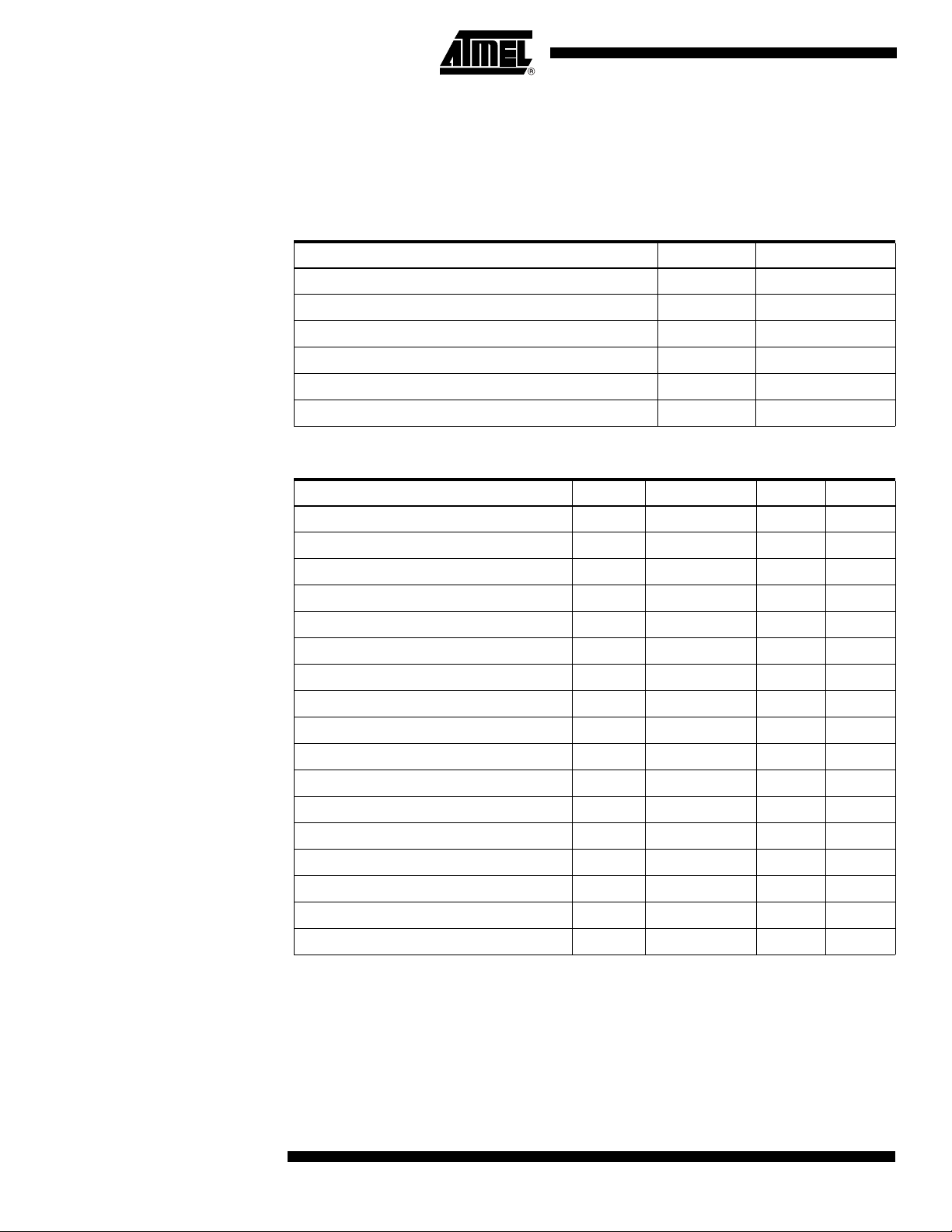
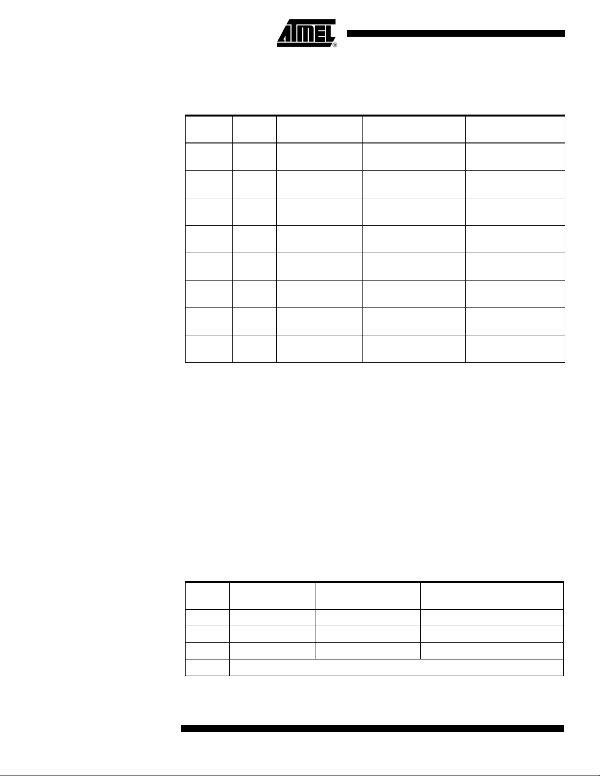
I/O Memory The I/O space definition of the ATtiny26(L) is shown in Table 2
Table 2 . ATtiny26(L) I/O Space
Address Hex Name Function
$3F ($5F) SREG Status Register
$3D ($5D) SP Stack Pointer
$3B ($5B) GIMSK General Interrupt Mask Register
$3A ($5A) GIFR General Interrupt Flag Register
$39 ($59) TIMSK Timer/Counter Interrupt Mask Register
$38 ($58) TIFR Timer/Counter Interrupt Flag Register
$35 ($55) MCUCR MCU Control Register
$34 ($54) MCUSR MCU Status Register
$33 ($53) TCCR0 Timer/Counter0 Control Register
$32 ($52) TCNT0 Timer/Counter0 (8-bit)
$31 ($51) OSCCAL Oscillator Calibration Register
$30 ($50) TCCR1A Timer/Counter1 Control Register A
$2F ($4F) TCCR1B Timer/Counter1 Control Register B
$2E ($4E) TCNT1 Timer/Counter1 (8-bit)
$2D ($4D) OCR1A Timer/Counter1 Output Compare Register A
$2C ($4C) OCR1B Timer/Counter1 Output Compare Register B
(1)
$2B ($4B) OCR1C Timer/Counter1 Output Compare Register C
$29 ($29) PLLCSR PLL Control and Status Register
$21 ($41) WDTCR Watchdog Timer Control Register
$1E ($3E) EEAR EEPROM Address Register
$1D ($3D) EEDR EEPROM Data Register
$1C ($3C) EECR EEPROM Control Register
$1B ($3B) PORTA Data Register, Port A
$1A ($3A) DDRA Data Direction Register, Port A
$19 ($39) PINA Input Pins, Port A
$18 ($38) PORTB Data Register, Port B
$17 ($37) DDRB Data Direction Register, Port B
$16 ($36) PINB Input Pins, Port B
$0F ($2F) USIDR Universal Serial Interface Data Register
$0E ($2E) USISR Universal Serial Interface Status Register
$0D ($2D) USICR Universal Serial Interface Control Register
$08 ($28) ACSR Analog Comparator Control and Status Register
$07 ($27) ADMUX ADC Multiplexer Select Register
20
ATtiny26(L)
1477F–AVR–12/04

ATtiny26(L)
Table 2 . ATtiny26(L) I/O Space
Address Hex Name Function
$06($26) ADCSR ADC Control and Status Register
$05($25) ADCH ADC Data Register High
$04($24) ADCL ADC Data Register Low
Note: 1. Reserved and unused locations are not shown in the table.
(1)
(Continued)
All ATtiny26(L) I/O and peripheral registers are placed in the I/O space. The I/O locations are accessed by the IN and OUT instructions transferring data between the 32
general purpose working registers and the I/O space. I/O Registers within the address
range $00 - $1F are directly bit-accessible using the SBI and CBI instructions. In these
registers, the value of single bits can be checked by using the SBIS and SBIC instructions. Refer to the instruction set chapter for more details. For compatibility with future
devices, reserved bits should be written zero if accessed. Reserved I/O memory
addresses should never be written.
1477F–AVR–12/04
21
System Clock and Clock Options
Clock Systems and their Distribution
Figure 20 presents the principal clock systems in the AVR and their distribution. All of
the clocks need not be active at a given time. In order to reduce power consumption, the
clocks to modules not being used can be halted by using different sleep modes, as
described in “Power Management and Sleep Modes” on page 36. The clock systems
are detailed below.
Figure 20. Clock Distribution
Timer/Counter1
General I/O
modules
clk
I/O
ADC CPU Core RAM
clk
ADC
AVR Clock
Control Unit
Clock
Multiplexer
Source clock
clk
CPU
clk
FLASH
Reset Logic
Watchdog Timer
Watchdog clock
Watchdog
Oscillator
Flash and
EEPROM
CPU Clock – clk
I/O Clock – clk
I/O
Flash Clock – clk
ADC Clock – clk
CPU
FLASH
ADC
clk
clk
PCK
PLL
PLL
External RC
Oscillator
External clock
Crystal
Oscillator
Low-Frequency
Crystal Oscillator
Calibrated RC
Oscillator
The CPU clock is routed to parts of the system concerned with operation of the AVR
core. Examples of such modules are the General Purpose Register File, the Status Register and the data memory holding the Stack Pointer. Halting the CPU clock inhibits the
core from performing general operations and calculations.
The I/O clock is used by the majority of the I/O modules, like Timer/Counters, and USI.
The I/O clock is also used by the External Interrupt module, but note that some external
interrupts are detected by asynchronous logic, allowing such interrupts to be detected
even if the I/O clock is halted.
The Flash clock controls operation of the Flash interface. The Flash clock is usually
active simultaneously with the CPU clock.
The ADC is provided with a dedicated clock domain. This allows halting the CPU and
I/O clocks in order to reduce noise generated by digital circuitry. This gives more accurate ADC conversion results.
22
ATtiny26(L)
1477F–AVR–12/04
ATtiny26(L)
Internal PLL for Fast
Peripheral Clock Generation –
clk
PCK
The internal PLL in ATtiny26(L) generates a clock frequency that is 64x multiplied from
nominally 1 MHz input. The source of the 1 MHz PLL input clock is the output of the
internal RC Oscillator which is automatically divided down to 1 MHz, if needed. See the
Figure 21 on page 23. When the PLL reference frequency is the nominal 1 MHz, the fast
peripheral clock is 64 MHz. The fast peripheral clock, or a clock prescaled from that, can
be selected as the clock source for Timer/Counter1.
The PLL is locked on the RC Oscillator and adjusting the RC Oscillator via OSCCAL
Register will adjust the fast peripheral clock at the same time. However, even if the possibly divided RC Oscillator is taken to a higher frequency than 1 MHz, the fast peripheral
clock frequency saturates at 70 MHz (worst case) and remains oscillating at the maximum frequency. It should be noted that the PLL in this case is not locked any more with
the RC Oscillator clock.
Therefore it is recommended not to take the OSCCAL adjustments to a higher frequency than 1 MHz in order to keep the PLL in the correct operating range. The internal
PLL is enabled only when the PLLE bit in the register PLLCSR is set or the PLLCK Fuse
is programmed (“0”). The bit PLOCK from the register PLLCSR is set when PLL is
locked.
Both internal 1 MHz RC Oscillator and PLL are switched off in Power-down and Standby
sleep modes.
Figure 21. PCK Clocking System
PLLE
RC OSCILLATOR
XTAL1
XTAL2
OSCCAL
1
2
4
8 MHz
OSCILLATORS
PLLCK &
CKSEL
FUSES
DIVIDE
TO 1 MHz
PLL
64x
Lock
Detector
PLOCK
PCK
DIVIDE
BY 4
CK
1477F–AVR–12/04
23
Clock Sources The device has the following clock source options, selectable by Flash Fuse bits as
shown below on Table 3. The clock from the selected source is input to the AVR clock
generator, and routed to the appropriate modules.The use of pins PB5 (XTAL2), and
PB4 (XTAL1) as I/O pins is limited depending on clock settings, as shown below in
Table 4.
Table 3 . Device Clocking Options Select
Device Clocking Option PLLCK CKSEL3..0
External Crystal/Ceramic Resonator 1 1111 - 1010
External Low-frequency Crystal 1 1001
External RC Oscillator 1 1000 - 0101
Calibrated Internal RC Oscillator 1 0100 - 0001
External Clock 1 0000
PLL Clock 0 0001
Table 4 . PB5, and PB4 Functionality vs. Device Clocking Options
Device Clocking Option PLLCK CKSEL [3:0] PB4 PB5
External Clock 1 0000 XTAL1 I/O
Internal RC Oscillator 1 0001 I/O I/O
Internal RC Oscillator 1 0010 I/O I/O
Internal RC Oscillator 1 0011 I/O I/O
Internal RC Oscillator 1 0100 I/O I/O
External RC Oscillator 1 0101 XTAL1 I/O
External RC Oscillator 1 0110 XTAL1 I/O
External RC Oscillator 1 0111 XTAL1 I/O
External RC Oscillator 1 1000 XTAL1 I/O
External Low-frequency Oscillator 1 1001 XTAL1 XTAL2
External Crystal/Resonator Oscillator 1 1010 XTAL1 XTAL2
External Crystal/Resonator Oscillator 1 1011 XTAL1 XTAL2
External Crystal/Resonator Oscillator 1 1100 XTAL1 XTAL2
External Crystal/Resonator Oscillator 1 1101 XTAL1 XTAL2
External Crystal/Resonator Oscillator 1 1110 XTAL1 XTAL2
External Crystal/Resonator Oscillator 1 1111 XTAL1 XTAL2
(1)
24
PLL 0 0001 I/O I/O
Note: 1. For all fuses “1” means unprogrammed while “0” means programmed.
The various choices for each clocking option is given in the following sections. When the
CPU wakes up from Power-down, the selected clock source is used to time the start-up,
ensuring stable oscillator operation before instruction execution starts. When the CPU
starts from Reset, there is as an additional delay allowing the power to reach a stable
level before commencing normal operation. The Watchdog Oscillator is used for timing
this real-time part of the start-up time. The number of WDT Oscillator cycles used for
ATtiny26(L)
1477F–AVR–12/04
ATtiny26(L)
each time-out is shown in Table 5. The frequency of the Watchdog Oscillator is voltage
dependent as shown in the Electrical Characteristics section.
Table 5 . Number of Watchdog Oscillator Cycles
Typ Time-out (VCC = 5.0V) Typ Time-out (VCC = 3.0V) Number of Cycles
4.1 ms 4.3 ms 4K (4,096)
65 ms 69 ms 64K (65,536)
Default Clock Source The deviced is shipped with CKSEL = “0001”, SUT = “10”, and PLLCK unprogrammed.
The default clock source setting is therefore the internal RC Oscillator with longest startup time. This default setting ensures that all users can make their desired clock source
setting using an In-System or Parallel Programmer.
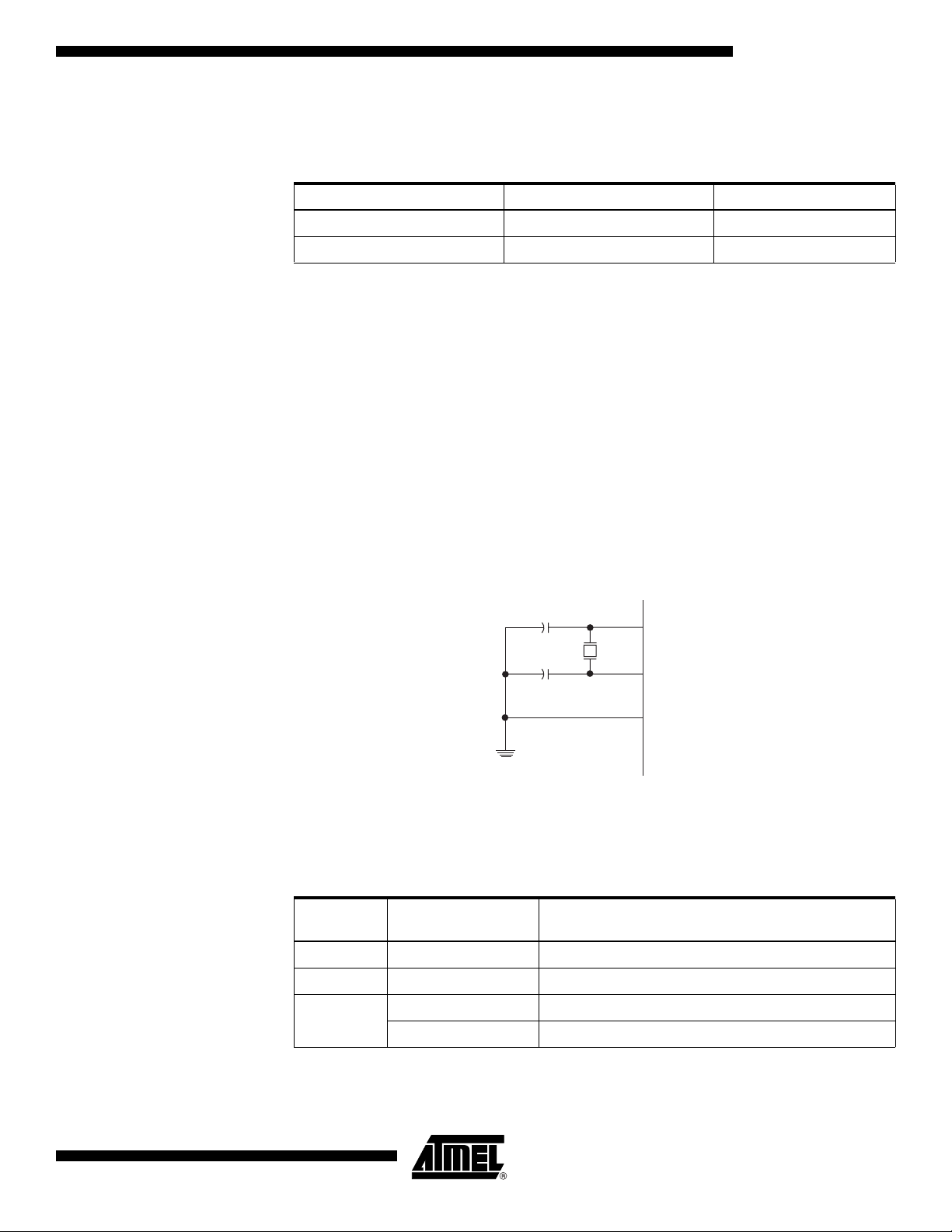
Crystal Oscillator XTAL1 and XTAL2 are input and output, respectively, of an inverting amplifier which can
be configured for use as an On-chip Oscillator, as shown in Figure 22. Either a quartz
crystal or a ceramic resonator may be used. The maximum frequency for resonators is
12 MHz. The CKOPT Fuse should always be unprogrammed when using this clock
option. C1 and C2 should always be equal. The optimal value of the capacitors depends
on the crystal or resonator in use, the amount of stray capacitance, and the electromagnetic noise of the environment. Some initial guidelines for choosing capacitors for use
with crystals are given in Table 6. For ceramic resonators, the capacitor values given by
the manufacturer should be used.
Figure 22. Crystal Oscillator Connections
C2
C1
XTAL2
XTAL1
GND
The Oscillator can operate in three different modes, each optimized for a specific frequency range. The operating mode is selected by the fuses CKSEL3..1 as shown in
Table 6.
Table 6 . Crystal Oscillator Operating Modes
Frequency
CKSEL3..1
(1)
101
110 0.9 - 3.0 12 - 22
111
Range (MHz)
0.4 - 0.9 –
3.0 - 16 12 - 22
16 - 12 - 15
Recommended Range for Capacitors C1 and
C2 for Use with Crystals (pF)
1477F–AVR–12/04
Note: 1. This option should not be used with crystals, only with ceramic resonators.
25
The CKSEL0 Fuse together with the SUT1..0 Fuses select the start-up times as shown
in Table 7.
Table 7 . Start-up Times for the Crystal Oscillator Clock Selection
Start-up Time
CKSEL0 SUT1..0
0 00 258 CK
0 01 258 CK
010 1K CK
011 1K CK
100 1K CK
1 01 16K CK – Crystal Oscillator,
1 10 16K CK 4.1 ms Crystal Oscillator, fast
1 11 16K CK 65 ms Crystal Oscillator,
Notes: 1. These options should only be used when not operating close to the maximum fre-
quency of the device, and only if frequency stability at start-up is not important for the
application.
2. These options are intended for use with ceramic resonators and will ensure frequency stability at start-up. They can also be used with crystals when not operating
close to the maximum frequency of the device, and if frequency stability at start-up is
not important for the application.
from Power-down
(1)
(1)
(2)
(2)
(2)
Additional Delay from
Reset (VCC = 5.0V)
4.1 ms Ceramic resonator,
65 ms Ceramic resonator,
– Ceramic resonator,
4.1 ms Ceramic resonator,
65 ms Ceramic resonator,
Recommended
Usage
fast rising power
slowly rising power
BOD enabled
fast rising power
slowly rising power
BOD enabled
rising power
slowly rising power
Low-frequency Crystal Oscillator
26
ATtiny26(L)
To use a 32.768 kHz watch crystal as the clock source for the device, the Low-frequency Crystal Oscillator must be selected by setting the PLLCK to “1” and CKSEL
Fuses to “1001”. The crystal should be connected as shown in Figure 22. By programming the CKOPT Fuse, the user can enable internal capacitors on XTAL1 and XTAL2,
thereby removing the need for external capacitors. The internal capacitors have a nominal value of 36 pF.
When this oscillator is selected, start-up times are determined by the SUT Fuses as
shown in Table 8.
Table 8 . Start-up Times for the Low-frequency Crystal Oscillator Clock Selection
Start-up Time
SUT1..0
00 1K CK
01 1K CK
10 32K CK 65 ms Stable frequency at start-up
11 Reserved
Note: 1. These options should only be used if frequency stability at start-up is not important
from Power-down
(1)
(1)
for the application.
Additional Delay from
Reset (VCC = 5.0V) Recommended Usage
4.1 ms Fast rising power or BOD enabled
65 ms Slowly rising power
1477F–AVR–12/04
ATtiny26(L)
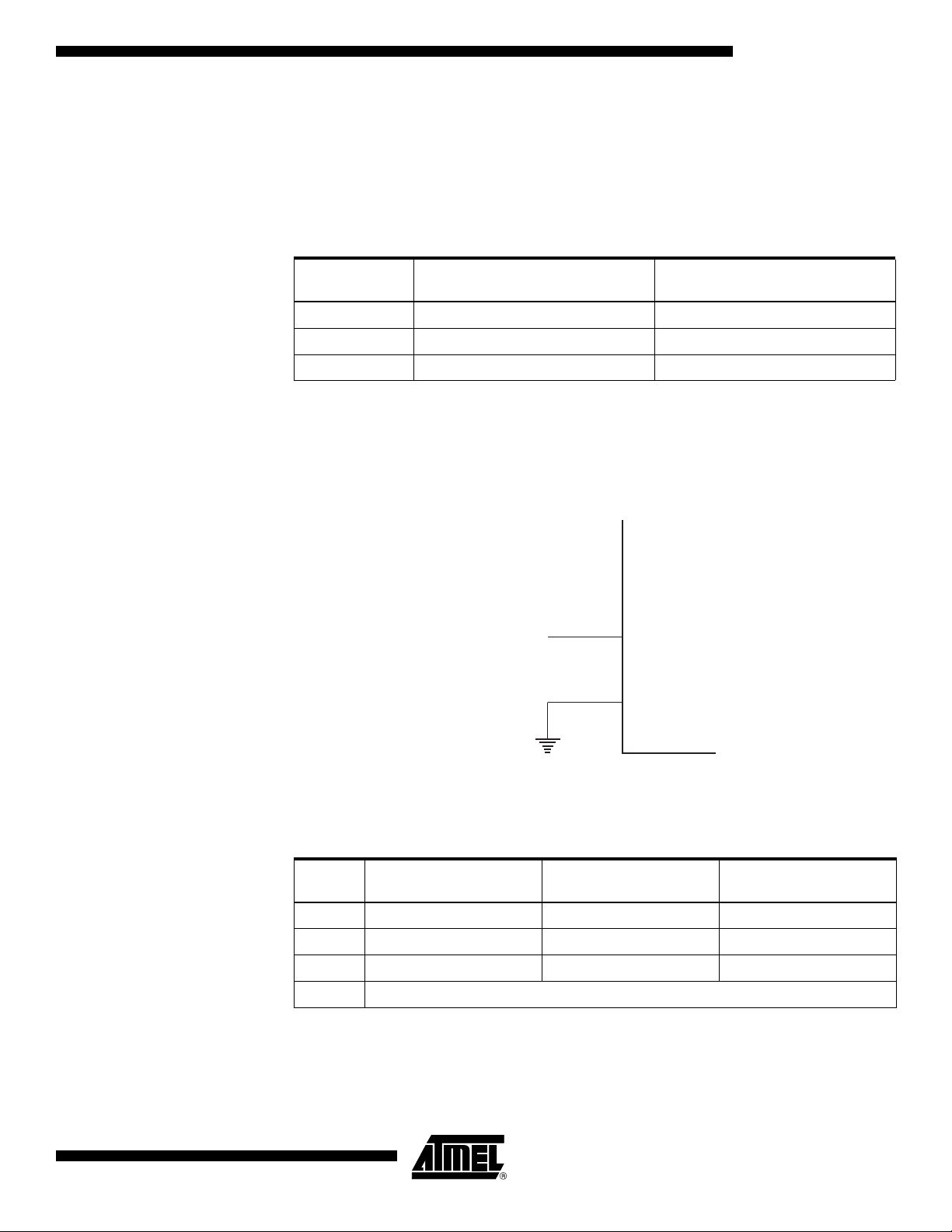
External RC Oscillator For timing insensitive applications, the external RC configuration shown in Figure 23
can be used. The frequency is roughly estimated by the equation f = 1/(3RC). C should
be at least 22 pF. By programming the CKOPT Fuse, the user can enable an internal
36 pF capacitor between XTAL1 and GND, thereby removing the need for an external
capacitor.
Figure 23. External RC Configuration
V
CC
PB5 (XTAL2)
R
XTAL1
C
GND
The oscillator can operate in four different modes, each optimized for a specific frequency range. The operating mode is selected by the fuses CKSEL3..0 as shown in
Table 9.
Table 9 . External RC Oscillator Operating Modes
CKSEL3..0 Frequency Range (MHz)
0101 0.1 - 0.9
0110 0.9 - 3.0
0111 3.0 - 8.0
1000 8.0 - 12.0
When this oscillator is selected, start-up times are determined by the SUT Fuses as
shown in Table 10.
Table 10. Start-up Times for the External RC Oscillator Clock Selection
1477F–AVR–12/04
Start-up Time
SUT1..0
00 18 CK – BOD enabled
01 18 CK 4.1 ms Fast rising power
10 18 CK 65 ms Slowly rising power
11 6 CK
Notes: 1. This option should not be used when operating close to the maximum frequency of
from Power-down
(1)
the device.
Additional Delay from
Reset (VCC = 5.0V) Recommended Usage
4.1 ms Fast rising power or BOD enabled
27
Calibrated Internal RC Oscillator
The calibrated internal RC Oscillator provides a fixed 1.0, 2.0, 4.0, or 8.0 MHz clock. All
frequencies are nominal values at 5V and 25°C. This clock may be selected as the system clock by programming the CKSEL Fuses as shown in Table 11. If selected, it will
operate with no external components. The CKOPT Fuse should always be unprogrammed when using this clock option. During Reset, hardware loads the calibration
byte into the OSCCAL Register and thereby automatically calibrates the RC Oscillator.
At 5V, 25°C and 1.0 MHz Oscillator frequency selected, this calibration gives a frequency within ± 3% of the nominal frequency. Using run-time calibration methods as
described in application notes available at www.atmel.com/avr it is possible to achieve ±
1% accuracy at any given V
and Temperature. When this oscillator is used as the chip
CC
clock, the Watchdog Oscillator will still be used for the Watchdog Timer and for the reset
time-out. For more information on the pre-programmed calibration value, see the section
“Calibration Byte” on page 109.
Table 11. Internal Calibrated RC Oscillator Operating Modes
CKSEL3..0 Nominal Frequency (MHz)
(1)
0001
0010 2.0
0011 4.0
0100 8.0
Note: 1. The device is shipped with this option selected.
1.0
When this oscillator is selected, start-up times are determined by the SUT Fuses as
shown in Table 12. PB4 (XTAL1) and PB5 (XTAL2) can be used as general I/O ports.
Oscillator Calibration Register
– OSCCAL
Table 12. Start-up Times for the Internal Calibrated RC Oscillator Clock Selection
Start-up Time from
SUT1..0
00 6 CK – BOD enabled
01 6 CK 4.1 ms Fast rising power
(1)
10
11 Reserved
Note: 1. The device is shipped with this option selected.
Bit 76543210
$31 ($51) CAL7 CAL6 CAL5 CAL4 CAL3 CAL2 CAL1 CAL0 OSCCAL
Read/Write R/W R/W R/W R/W R/W R/W R/W R/W
Initial Value Device Specific Calibration Value
Power-down
6 CK 65 ms Slowly rising power
Additional Delay from
Reset (VCC = 5.0V) Recommended Usage
• Bits 7..0 – CAL7..0: Oscillator Calibration Value
Writing the calibration byte to this address will trim the internal oscillator to remove process variations from the oscillator frequency. During Reset, the 1 MHz calibration value
which is located in the signature row high byte (address 0x00) is automatically loaded
into the OSCCAL Register. If the internal RC is used at other frequencies, the calibration
value must be loaded manually. This can be done by first reading the signature row by a
programmer, and then store the calibration values in the Flash or EEPROM. Then the
value can be read by software and loaded into the OSCCAl Register. When OSCCAL is
zero, the lowest available frequency is chosen. Writing non-zero values to this register
28
ATtiny26(L)
1477F–AVR–12/04
ATtiny26(L)
will increase the frequency of the internal oscillator. Writing $FF to the register gives the
highest available frequency. The calibrated Oscillator is used to time EEPROM and
Flash access. If EEPROM or Flash is written, do not calibrate to more than 10% above
the nominal frequency. Otherwise, the EEPROM or Flash write may fail. Note that the
oscillator is intended for calibration to 1.0, 2.0, 4.0, or 8.0 MHz. Tuning to other values is
not guaranteed, as indicated in Table 13.
Table 13. Internal RC Oscillator Frequency Range.
Min Frequency in Percentage of
OSCCAL Value
$00 50% 100%
$7F 75% 150%
$FF 100% 200%
Nominal Frequency
Max Frequency in Percentage of
Nominal Frequency
External Clock To drive the device from an external clock source, XTAL1 should be driven as shown in
Figure 24. To run the device on an external clock, the CKSEL Fuses must be programmed to “0000” and PLLCK to “1”. By programming the CKOPT Fuse, the user can
enable an internal 36 pF capacitor between XTAL1 and GND.
Figure 24. External Clock Drive Configuration
PB5 (XTAL2)
EXTERNAL
CLOCK
SIGNAL
XTAL1
GND
1477F–AVR–12/04
When this clock source is selected, start-up times are determined by the SUT Fuses as
shown in Table 14.
Table 14. Start-up Times for the External Clock Selection
Start-up Time from
SUT1..0
00 6 CK – BOD enabled
01 6 CK 4.1 ms Fast rising power
10 6 CK 65 ms Slowly rising power
11 Reserved
Power-down
Additional Delay from
Reset (VCC = 5.0V) Recommended Usage
When applying an external clock, it is required to avoid sudden changes in the applied
clock frequency to ensure stable operation of the MCU. A variation in frequency of more
than 2% from one clock cycle to the next can lead to unpredictable behaviour. It is
required to ensure that the MCU is kept in reset during such changes in the clock
frequency.
29

High Frequency PLL
Clock – PLL
CLK
There is an internal PLL that provides nominally 64 MHz clock rate locked to the RC
Oscillator for the use of the Peripheral Timer/Counter1 and for the system clock source.
When selected as a system clock source, by programming (“0”) the fuse PLLCK, it is
divided by four. When this option is used, the CKSEL3..0 must be set to “0001”. This
clocking option can be used only when operating between 4.5 - 5.5V to guaratee safe
operation. The system clock frequency will be 16 MHz (64 MHz/4). When using this
clock option, start-up times are determined by the SUT Fuses as shown in Table 15.
See also “PCK Clocking System” on page 23.
Table 15. Start-up Times for the PLLCK
Start-up Time from
SUT1..0
00 1K CK – BOD enabled
01 1K CK 4.1 ms Fast rising power
10 1K CK 65 ms Slowly rising power
11 16K CK – Slowly rising power
Power-down
Additional Delay from
Reset (VCC = 5.0V) Recommended Usage
30
ATtiny26(L)
1477F–AVR–12/04

ATtiny26(L)
System Control and Reset
The ATtiny26(L) provides four sources of reset:
Power-on Reset. The MCU is reset when the supply voltage is below the Power-on Reset
•
threshold (V
POT
).
• External Reset. To use the PB7/RESET pin as an External Reset, instead of I/O pin,
unprogram (“1”) the RSTDISBL Fuse. The MCU is reset when a low level is present on the
pin for more than 50 ns.
RESET
• Watchdog Reset. The MCU is reset when the Watchdog timer period expires and the
Watchdog is enabled.
• Brown-out Reset. The MCU is reset when the supply voltage V
Reset threshold (V
BOT
).
is below the Brown-out
CC
During reset, all I/O Registers are then set to their initial values, and the program starts
execution from address $000. The instruction placed in address $000 must be an RJMP
– Relative Jump – instruction to the reset handling routine. If the program never enables
an interrupt source, the interrupt vectors are not used, and regular program code can be
placed at these locations. Figure 25 shows the reset logic for the ATtiny26(L). Table 16
shows the timing and electrical parameters of the reset circuitry for ATtiny26(L).
Figure 25. Reset Logic for the ATtiny26(L)
DATA BU S
MCU Status
Register (MCUSR)
BORF
PORF
WDRF
EXTRF
BODEN
BODLEVEL
Brown-Out
Reset Circuit
Clock
Generator
CKSEL[3:0]
CK
Delay Counters
TIMEOUT
1477F–AVR–12/04
31

Table 16. Reset Characteristics
Symbol Parameter Condition Min Typ Max Units
Power-on Reset Threshold
Voltage (rising)
V
V
V
V
POT
RST
t
RST
BOT
t
BOD
HYST
Power-on Reset Threshold
Voltage (falling)
(1)
RESET Pin Threshold Voltage 0.2 0.9 V
Minimum pulse width on
RESET Pin
Brown-out Reset Threshold
(2)
Voltage
Minimum low voltage period for
Brown-out Detection
BODLEVEL = 1 2.4 2.7 2.9
BODLEVEL = 0 3.7 4.0 4.5
BODLEVEL = 1 2 µs
BODLEVEL = 0 2 µs
Brown-out Detector hysteresis 130 mV
Notes: 1. The Power-on Reset will not work unless the supply voltage has been below V
1.4 2.3 V
1.3 2.3 V
CC
1.5 µs
V
POT
(falling)
2. V
may be below nominal minimum operating voltage for some devices. For
BOT
devices where this is the case, the device is tested down to VCC = V
during the
BOT
production test. This guarantees that a Brown-out Reset will occur before V
CC
drops
to a voltage where correct operation of the microcontroller is no longer guaranteed.
The test is performed using BODLEVEL=1 for ATtiny26L and BODLEVEL=0 for
ATtiny26. BODLEVEL=1 is not applicable for ATtiny26.
See start-up times from reset from “System Clock and Clock Options” on page 22.
When the CPU wakes up from Power-down, only the clock counting part of the start-up
time is used. The Watchdog Oscillator is used for timing the real-time part of the start-up
time.
Power-on Reset A Power-on Reset (POR) pulse is generated by an On-chip Detection circuit. The detec-
32
ATtiny26(L)
tion level is defined in Table 16 The POR is activated whenever V
detection level. The POR circuit can be used to trigger the Start-up Reset, as well as
detect a failure in supply voltage.
The Power-on Reset (POR) circuit ensures that the device is reset from Power-on.
Reaching the Power-on Reset threshold voltage invokes a delay counter, which determines the delay, for which the device is kept in RESET after V
CC
period of the delay counter can be defined by the user through the CKSEL Fuses. The
different selections for the delay period are presented in “System Clock and Clock
Options” on page 22. The RESET signal is activated again, without any delay, when the
V
decreases below detection level.
CC
is below the
CC
rise. The time-out
1477F–AVR–12/04

Figure 26. MCU Start-up, RESET Tied to VCC
V
VCC
RESET
TIME-OUT
INTERNAL
RESET
POT
V
RST
t
TOUT
ATtiny26(L)
Figure 27. MCU Start-up, RESET
V
VCC
RESET
TIME-OUT
INTERNAL
RESET
POT
Controlled Externally
V
RST
t
TOUT
External Reset An External Reset is generated by a low level on the RESET pin. Reset pulses longer
than 500 ns will generate a reset, even if the clock is not running. Shorter pulses are not
guaranteed to generate a reset. When the applied signal reaches the Reset Threshold
Voltage – V
period t
TOUT
Figure 28. External Reset During Operation
VCC
– on its positive edge, the delay timer starts the MCU after the Time-out
RST
has expired.
1477F–AVR–12/04
RESET
TIME-OUT
INTERNAL
RESET
V
RST
t
TOUT
33

Brown-out Detection ATtiny26(L) has an On-chip Brown-out Detection (BOD) circuit for monitoring the V
level during the operation. The BOD circuit can be enabled/disabled by the fuse
BODEN. When the BOD is enabled (BODEN programmed), and V
the trigger level, the Brown-out Reset is immediately activated. When V
above the trigger level, the Brown-out Reset is deactivated after a delay. The delay is
defined by the user in the same way as the delay of POR signal, in Table 29. The trigger
level for the BOD can be selected by the fuse BODLEVEL to be 2.7V (BODLEVEL
unprogrammed), or 4.0V (BODLEVEL programmed). The trigger level has a hysteresis
of 50 mV to ensure spike free Brown-out Detection.
decreases below
CC
increases
CC
CC
The BOD circuit will only detect a drop in V
for longer than t
given in Table 16.
BOD
if the voltage stays below the trigger level
CC
Figure 29. Brown-out Reset During Operation
V
CC
V
BOT-
V
BOT+
RESET
t
TIME-OUT
TOUT
INTERNAL
RESET
Watchdog Reset When the Watchdog times out, it will generate a short reset pulse of one CK cycle dura-
tion. On the falling edge of this pulse, the delay timer starts counting the Time-out period
t
. Refer to page 78 for details on operation of the Watchdog.
TOUT
34
Figure 30. Watchdog Time-out
1 CK Cycle
ATtiny26(L)
1477F–AVR–12/04

ATtiny26(L)
MCU Status Register –
MCUSR
Bit 76543210
$34 ($54) ––––WDRFBORFEXTRFPORFMCUSR
Read/Write R R R R R/W R/W R/W R/W
Initial Value0000 See Bit Description
• Bit 7..4 – Res: Reserved Bits
These bits are reserved bits in the ATtiny26(L) and always read as zero.
• Bit 3 – WDRF: Watchdog Reset Flag
This bit is set (one) if a Watchdog Reset occurs. The bit is reset (zero) by a Power-on
Reset, or by writing a logic zero to the flag.
• Bit 2 – BORF: Brown-out Reset Flag
This bit is set (one) if a Brown-out Reset occurs. The bit is reset (zero) by a Power-on
Reset, or by writing a logic zero to the flag.
• Bit 1 – EXTRF: External Reset Flag
This bit is set (one) if an External Reset occurs. The bit is reset (zero) by a Power-on
Reset, or by writing a logic zero to the flag.
• Bit 0 – PORF: Power-on Reset Flag
This bit is set (one) if a Power-on Reset occurs. The bit is reset (zero) by writing a logic
zero to the flag.
To make use of the reset flags to identify a reset condition, the user should read and
then reset (zero) the MCUSR as early as possible in the program. If the register is
cleared before another reset occurs, the source of the reset can be found by examining
the reset flags.
1477F–AVR–12/04
35

Power Management and Sleep Modes
Sleep modes enable the application to shut down unused modules in the MCU, thereby
saving power. The AVR provides various sleep modes allowing the user to tailor the
power consumption to the application’s requirements.
To enter any of the four sleep modes, the SE bit in MCUCR must be written to logic one
and a SLEEP instruction must be executed. The SM1, and SM0 bits in the MCUCR
Register select which sleep mode (Idle, ADC Noise Reduction, Power Down, or Standby) will be activated by the SLEEP instruction. See Table 17 for a summary. If an
enabled interrupt occurs while the MCU is in a sleep mode, the MCU wakes up. The
MCU is then halted for four cycles in addition to the start-up time, it executes the interrupt routine, and resumes execution from the instruction following SLEEP. The contents
of the Register File and SRAM are unaltered when the device wakes up from sleep. If a
Reset occurs during sleep mode, the MCU wakes up and executes from the Reset
Vector.
Table 19 on page 38 presents the different clock systems in the ATtiny26, and their distribution. The figure is helpful in selecting an appropriate sleep mode.
MCU Control Register –
MCUCR
The MCU Control Register contains control bits for general MCU functions.
Bit 76543210
$35 ($55) – PUD SE SM1 SM0 – ISC01 ISC00 MCUCR
Read/Write R R/W R/W R/W R/W R R/W R/W
Initial Value00000000
• Bits 7 – Res: Reserved Bit
This bit is a reserved bit in the ATtiny26(L) and always reads as zero.
• Bit 6 – PUD: Pull-up Disable
When this bit is set (one), the pull-ups in the I/O ports are disabled even if the DDxn and
PORTxn Registers are configured to enable the pull-ups ({DDxn, PORTxn} = 0b01). See
“Configuring the Pin” on page 42 for more details about this feature.
• Bit 5 – SE: Sleep Enable
The SE bit must be set (one) to make the MCU enter the Sleep mode when the SLEEP
instruction is executed. To avoid the MCU entering the Sleep mode unless it is the programmers purpose, it is recommended to set the Sleep Enable SE bit just before the
execution of the SLEEP instruction.
• Bits 4,3 – SM1/SM0: Sleep Mode Select Bits 1 and 0
These bits select between the four available Sleep modes, as shown in the following
table.
Table 17. Sleep Modes
36
SM1 SM0 Sleep Mode
0 0 Idle mode
0 1 ADC Noise Reduction mode
1 0 Power-down mode
1 1 Standby mode
For details, refer to the paragraph “Sleep Modes” below.
• Bit 2 – Res: Reserved Bit
This bit is a reserved bit in the ATtiny26(L) and always reads as zero.
ATtiny26(L)
1477F–AVR–12/04

ATtiny26(L)
• Bits 1, 0 – ISC01, ISC00: Interrupt Sense Control 0 Bit 1 and Bit 0
The External Interrupt 0 is activated by the external pin INT0 if the SREG I-flag and the
corresponding interrupt mask is set (one). The activity on the external INT0 pin that activates the interrupt is defined in the following table.
Table 18. Interrupt 0 Sense Control
ISC01 ISC00 Description
0 0 The low level of INT0 generates an interrupt request.
0 1 Any change on INT0 generates an interrupt request.
1 0 The falling edge of INT0 generates an interrupt request.
1 1 The rising edge of INT0 generates an interrupt request.
Note: 1. When changing the ISC10/ISC00 bits, INT0 must be disabled by clearing its Interrupt
Enable bit in the GIMSK Register. Otherwise an interrupt can occur when the bits are
changed.
(1)
Idle Mode When the SM1..0 bits are written to “00”, the SLEEP instruction makes the MCU enter
Idle mode, stopping the CPU but allowing Analog Comparator, ADC, USI,
Timer/Counters, Watchdog, and the interrupt system to continue operating. This sleep
mode basically halts clk
Idle mode enables the MCU to wake up from external triggered interrupts as well as
internal ones like the Timer Overflow and USI Start and Overflow interrupts. If wake-up
from the Analog Comparator interrupt is not required, the Analog Comparator can be
powered down by setting the ACD bit in the Analog Comparator Control and Status
Register – ACSR. This will reduce power consumption in Idle mode. If the ADC is
enabled, a conversion starts automatically when this mode is entered.
CPU
and clk
, while allowing the other clocks to run.
FLASH
ADC Noise Reduction Mode
When the SM1..0 bits are written to “01”, the SLEEP instruction makes the MCU enter
ADC Noise Reduction mode, stopping the CPU but allowing the ADC, the External Interrupts, the USI start condition detection, and the Watchdog to continue operating (if
enabled). This sleep mode basically halts clk
I/O
, clk
, and clk
CPU
, while allowing the
FLASH
other clocks to run.
This improves the noise environment for the ADC, enabling higher resolution measurements. If the ADC is enabled, a conversion starts automatically when this mode is
entered. Apart form the ADC Conversion Complete interrupt, only an External Reset, a
Watchdog Reset, a Brown-out Reset, USI start condition interrupt, an EEPROM ready
interrupt, an External Level Interrupt on INT0, or a pin change interrupt can wake up the
MCU from ADC Noise Reduction mode.
Power-down Mode When the SM1..0 bits are written to “10”, the SLEEP instruction makes the MCU enter
Power-down mode. In this mode, the External Oscillator is stopped, while the External
Interrupts, the USI start condition detection, and the Watchdog continue operating (if
enabled). Only an External Reset, a Watchdog Reset, a Brown-out Reset, USI start condition interrupt, an External Level Interrupt on INT0, or a pin change interrupt can wake
up the MCU. This sleep mode basically halts all generated clocks, allowing operation of
asynchronous modules only.
When waking up from Power-down mode, there is a delay from the wake-up condition
occurs until the wake-up becomes effective. This allows the clock to restart and become
stable after having been stopped. The wake-up period is defined by the same CKSEL
Fuses that define the reset time-out period, as described in “Clock Sources” on page 24.
1477F–AVR–12/04
37

Note that if a level triggered external interrupt or pin change interrupt is used from
Power-down mode, the changed level must be held for some time to wake up the MCU.
This makes the MCU less sensitive to noise.
If the wake-up condition disappears before the MCU wakes up and starts to execute,
e.g., a low level on INT0 is not held long enough, the interrupt causing the wake-up will
not be executed.
Standby Mode When the SM1..0 bits are “11” and an External Crystal/Resonator clock option is
selected, the SLEEP instruction forces the MCU into the Standby mode. This mode is
identical to Power-down with the exception that the Oscillator is kept running. From
Standby mode, the device wakes up in only six clock cycles.
Table 19. Active Clock Domains and Wake-up Sources in the different Sleep Modes.
Active Clock domains Oscillators Wake-up Sources
Sleep Mode
clk
CPU
clk
FLASH
clkIOclk
ADC
Main Clock
Source Enabled
Idle X X X X X X X X
ADC Noise
Reduction X X X
Power-down X
Standby
(1)
XX
INT0, and Pin
Change
(2)
(2)
(2)
USI Start
Condition
EEPROM
Ready
ADC Other I/O
XXX
X
X
Notes: 1. Only recommended with external crystal or resonator selected as clock source.
2. Only level interrupt INT0.
38
ATtiny26(L)
1477F–AVR–12/04

ATtiny26(L)
Minimizing Power Consumption
There are several issues to consider when trying to minimize the power consumption in
an AVR controlled system. In general, sleep modes should be used as much as possible, and the sleep mode should be selected so that as few as possible of the device’s
functions are operating. All functions not needed should be disabled. In particular, the
following modules may need special consideration when trying to achieve the lowest
possible power consumption.
Analog to Digital Converter If enabled, the ADC will be enabled in all sleep modes. To save power, the ADC should
be disabled before entering any sleep mode. When the ADC is turned off and on again,
the next conversion will be an extended conversion. Refer to “Analog to Digital Converter” on page 94 for details on ADC operation.
Analog Comparator When entering Idle mode, the Analog Comparator should be disabled if not used. When
entering ADC Noise Reduction mode, the Analog Comparator should be disabled. In the
other sleep modes, the Analog Comparator is automatically disabled. However, if the
Analog Comparator is set up to use the Internal Voltage Reference as input, the Analog
Comparator should be disabled in all sleep modes. Otherwise, the Internal Voltage Reference will be enabled, independent of sleep mode. Refer to “Analog Comparator” on
page 91 for details on how to configure the Analog Comparator.
Brown-out Detector If the Brown-out Detector is not needed in the application, this module should be turned
off. If the Brown-out Detector is enabled by the BODEN Fuse, it will be enabled in all
sleep modes, and hence, always consume power. In the deeper sleep modes, this will
contribute significantly to the total current consumption. Refer to “Brown-out Detection”
on page 34 for details on how to configure the Brown-out Detector.
Internal Voltage Reference The Internal Voltage Reference (see Table 20) will be enabled when needed by the
Brown-out Detector, the Analog Comparator or the ADC. If these modules are disabled
as described in the sections above, the Internal Voltage Reference will be disabled and
it will not be consuming power. When turned on again, the user must allow the reference
to start up before the output is used. If the reference is kept on in sleep mode, the output
can be used immediately.
Table 20. Internal Voltage Reference
Symbol Parameter Min Typ Max Units
V
BG
t
BG
I
BG
Bandgap reference voltage 1.15 1.18 1.40 V
Bandgap reference start-up time 40 70 µs
Bandgap reference current consumption 10 µA
Watchdog Timer If the Watchdog Timer is not needed in the application, this module should be turned off.
If the Watchdog Timer is enabled, it will be enabled in all sleep modes, and hence,
always consume power. In the deeper sleep modes, this will contribute significantly to
the total current consumption. Refer to “Watchdog Timer” on page 78 for details on how
to configure the Watchdog Timer.
Port Pins When entering a sleep mode, all port pins should be configured to use minimum power.
The most important thing is then to ensure that no pins drive resistive loads. In sleep
modes where the both the I/O clock (clk
) and the ADC clock (clk
I/O
) are stopped, the
ADC
input buffers of the device will be disabled. This ensures that no power is consumed by
the input logic when not needed. In some cases, the input logic is needed for detecting
wake-up conditions, and it will then be enabled. Refer to “Digital Input Enable and Sleep
Modes” on page 45 for details on which pins are enabled. If the input buffer is enabled
1477F–AVR–12/04
39

and the input signal is left floating or have an analog signal level close to VCC/2, the
input buffer will use excessive power.
40
ATtiny26(L)
1477F–AVR–12/04

ATtiny26(L)
I/O Ports
Introduction All AVR ports have true Read-Modify-Write functionality when used as general digital
I/O ports. This means that the direction of one port pin can be changed without unintentionally changing the direction of any other pin with the SBI and CBI instructions. The
same applies when changing drive value (if configured as output) or enabling/disabling
of pull-up resistors (if configured as input). Each output buffer, except reset, has symmetrical drive characteristics with both high sink and source capability. The pin driver is
strong enough to drive LED displays directly. All port pins have individually selectable
pull-up resistors with a supply-voltage invariant resistance. All I/O pins have protection
diodes to both V
Figure 31. I/O Pin Equivalent Schematic
and Ground as indicated in Figure 31.
CC
R
pu
Pxn
C
pin
All registers and bit references in this section are written in general form. A lower case
“x” represents the numbering letter for the port, and a lower case “n” represents the bit
number. However, when using the register or bit defines in a program, the precise form
must be used. For example, PORTB3 for bit no. 3 in Port B, here documented generally
as PORTxn. The physical I/O Registers and bit locations are listed in “Register Description for I/O Ports” on page 56.
Three I/O memory address locations are allocated for each port, one each for the Data
Register – PORTx, Data Direction Register – DDRx, and the Port Input Pins – PINx. The
Port Input Pins I/O location is read only, while the Data Register and the Data Direction
Register are read/write. In addition, the Pull-up Disable – PUD bit in MCUCR disables
the pull-up function for all pins in all ports when set.
Using the I/O port as General Digital I/O is described in “Ports as General Digital I/O” on
page 42. Most port pins are multiplexed with alternate functions for the peripheral features on the device. How each alternate function interferes with the port pin is described
in “Alternate Port Functions” on page 46. Refer to the individual module sections for a
full description of the alternate functions.
See Figure
"General Digital I/O" for
Logic
Details
1477F–AVR–12/04
Note that enabling the alternate function of some of the port pins does not affect the use
of the other pins in the port as general digital I/O.
41

Ports as General Digital I/O
The ports are bi-directional I/O ports with optional internal pull-ups. Figure 32 shows a
functional description of one I/O-port pin, here generically called Pxn.
Figure 32. General Digital I/O
Pxn
PUD: PULLUP DISABLE
SLEEP: SLEEP CONTROL
clk
: I/O CLOCK
I/O
(1)
SLEEP
Q
D
DDxn
Q
CLR
RESET
Q
D
PORTxn
Q
CLR
RESET
SYNCHRONIZER
D
DLQ
WDx: WRITE DDRx
RDx: READ DDRx
WPx: WRITE PORTx
RRx: READ PORTx REGISTER
RPx: READ PORTx PIN
Q
PINxn
Q
Q
PUD
WDx
RDx
WPx
RRx
RPx
clk
DATA B US
I/O
Note: 1. WPx, WDx, RRx, RPx, and RDx are common to all pins within the same port. clk
I/O
SLEEP, and PUD are common to all ports.
Configuring the Pin Each port pin consists of 3 Register bits: DDxn, PORTxn, and PINxn. As shown in “Reg-
ister Description for I/O Ports” on page 56, the DDxn bits are accessed at the DDRx I/O
address, the PORTxn bits at the PORTx I/O address, and the PINxn bits at the PINx I/O
address.
The DDxn bit in the DDRx Register selects the direction of this pin. If DDxn is written
logic one, Pxn is configured as an output pin. If DDxn is written logic zero, Pxn is configured as an input pin.
If PORTxn is written logic one when the pin is configured as an input pin, the pull-up
resistor is activated. To switch the pull-up resistor off, PORTxn has to be written logic
zero or the pin has to be configured as an output pin. The port pins are tri-stated when a
reset condition becomes active, even if no clocks are running.
If PORTxn is written logic one when the pin is configured as an output pin, the port pin is
driven high (one). If PORTxn is written logic zero when the pin is configured as an output pin, the port pin is driven low (zero).
When switching between tri-state ({DDxn, PORTxn} = 0b00) and output high ({DDxn,
PORTxn} = 0b11), an intermediate state with either pull-up enabled ({DDxn, PORTxn} =
0b01) or output low ({DDxn, PORTxn} = 0b10) must occur. Normally, the pull-up
enabled state is fully acceptable, as a high-impedant environment will not notice the
,
42
ATtiny26(L)
1477F–AVR–12/04

ATtiny26(L)
difference between a strong high driver and a pull-up. If this is not the case, the PUD bit
in the MCUCR Register can be set to disable all pull-ups in all ports.
Switching between input with pull-up and output low generates the same problem. The
user must use either the tri-state ({DDxn, PORTxn} = 0b00) or the output high state
({DDxn, PORTxn} = 0b11) as an intermediate step.
Table 21 summarizes the control signals for the pin value.
Table 21. Port Pin Configurations
PUD
DDxn PORTxn
0 0 X Input No Tri-state (Hi-Z)
0 1 0 Input Yes
0 1 1 Input No Tri-state (Hi-Z)
1 0 X Output No Output Low (Sink)
1 1 X Output No Output High (Source)
Reading the Pin Value Independent of the setting of Data Direction bit DDxn, the port pin can be read through
the PINxn Register Bit. As shown in Figure 32, the PINxn Register bit and the preceding
latch constitute a synchronizer. This is needed to avoid metastability if the physical pin
changes value near the edge of the internal clock, but it also introduces a delay. Figure
33 shows a timing diagram of the synchronization when reading an externally applied
pin value. The maximum and minimum propagation delays are denoted t
respectively.
(in MCUCR) I/O Pull-up Comment
Pxn will source current if ext. pulled
low
pd,max
and t
pd,min
Figure 33. Synchronization when Reading an Externally Applied Pin Value
SYSTEM CLK
INSTRUCTIONS
SYNC LATCH
PINxn
r17
XXX in r17, PINx
XXX
0x00 0xFF
t
pd, max
t
pd, min
Consider the clock period starting shortly after the first falling edge of the system clock.
The latch is closed when the clock is low, and goes transparent when the clock is high,
as indicated by the shaded region of the “SYNC LATCH” signal. The signal value is
latched when the system clock goes low. It is clocked into the PINxn Register at the succeeding positive clock edge. As indicated by the two arrows t
pd,max
and t
pd,min
, a single
1477F–AVR–12/04
43

signal transition on the pin will be delayed between ½ and 1½ system clock period
depending upon the time of assertion.
When reading back a software assigned pin value, a nop instruction must be inserted as
indicated in Figure 34. The out instruction sets the “SYNC LATCH” signal at the positive
edge of the clock. In this case, the delay t
through the synchronizer is one system
pd
clock period.
Figure 34. Synchronization when Reading a Software Assigned Pin Value
SYSTEM CLK
r16
INSTRUCTIONS
SYNC LATCH
PINxn
r17
0xFF
out PORTx, r16 nop in r17, PINx
0x00 0xFF
t
pd
44
ATtiny26(L)
1477F–AVR–12/04

ATtiny26(L)
The following code example shows how to set port B pins 0 and 1 high, 2 and 3 low, and
define the port pins from 4 to 7 as input with pull-ups assigned to port pins 6 and 7. The
resulting pin values are read back again, but as previously discussed, a nop instruction
is included to be able to read back the value recently assigned to some of the pins.
Assembly Code Example
...
; Define pull-ups and set outputs high
; Define directions for port pins
ldi r16,(1<<PB7)|(1<<PB6)|(1<<PB1)|(1<<PB0)
ldi r17,(1<<DDB3)|(1<<DDB2)|(1<<DDB1)|(1<<DDB0)
out PORTB,r16
out DDRB,r17
; Insert nop for synchronization
nop
; Read port pins
in r16,PINB
...
C Code Example
(1)
Digital Input Enable and Sleep Modes
unsigned char i;
...
/* Define pull-ups and set outputs high */
/* Define directions for port pins */
PORTB = (1<<PB7)|(1<<PB6)|(1<<PB1)|(1<<PB0);
DDRB = (1<<DDB3)|(1<<DDB2)|(1<<DDB1)|(1<<DDB0);
/* Insert nop for synchronization*/
_NOP();
/* Read port pins */
i = PINB;
...
Note: 1. For the assembly program, two temporary registers are used to minimize the time
from pull-ups are set on pins 0, 1, 6, and 7, until the direction bits are correctly set,
defining bit 2 and 3 as low and redefining bits 0 and 1 as strong high drivers.
As shown in Figure 32, the digital input signal can be clamped to ground at the input of
the schmitt-trigger. The signal denoted SLEEP in the figure, is set by the MCU Sleep
Controller in Power-down mode, Standby mode, and ADC Noise Reduction mode to
avoid high power consumption if some input signals are left floating, or have an analog
signal level close to V
CC
/2.
SLEEP is overridden for port pins enabled as External Interrupt pins. If the External
Interrupt Request is not enabled, SLEEP is active also for these pins. SLEEP is also
overridden by various other alternate functions as described in “Alternate Port Functions” on page 46.
1477F–AVR–12/04
If a logic high level (“one”) is present on an Asynchronous External Interrupt pin configured as “Interrupt on a Rising Edge, Falling Edge, or Any Logic Change on Pin” while
the external interrupt is not enabled, the corresponding External Interrupt Flag will be set
when resuming from the above mentioned sleep modes, as the clamping in these sleep
modes produces the requested logic change.
45

Unconnected Pins If some pins are unused, it is recommended to ensure that these pins have a defined
level. Even though most of the digital inputs are disabled in the deep sleep modes as
described above, floating inputs should be avoided to reduce current consumption in all
other modes where the digital inputs are enabled (Reset, Active mode, and Idle mode).
The simplest method to ensure a defined level of an unused pin, is to enable the internal
pullup. In this case, the pullup will be disabled during reset. If low power consumption
during reset is important, it is recommended to use an external pullup or pulldown. Connecting unused pins directly to V
or GND is not recommended, since this may cause
CC
excessive currents if the pin is accidentally configured as an output.
Alternate Port Functions Most port pins have alternate functions in addition to being general digital I/Os. Figure
35 shows how the port pin control signals from the simplified Figure 32 can be overridden by alternate functions. The overriding signals may not be present in all port pins, but
the figure serves as a generic description applicable to all port pins in the AVR microcontroller family.
Figure 35. Alternate Port Functions
1
0
1
0
Pxn
1
0
1
0
(1)
PUOExn
PUOVxn
DDOExn
DDOVxn
PVOExn
PVOVxn
DIEOExn
DIEOVxn
SLEEP
SYNCHRONIZER
SET
DLQ
D
PINxn
Q
CLR
PUD
D
Q
DDxn
Q
CLR
RESET
D
Q
PORTxn
Q
CLR
RESET
Q
Q
CLR
WDx
RDx
WPx
RRx
RPx
clk
DATA B U S
I/O
46
ATtiny26(L)
DIxn
AIOxn
PUOExn: Pxn PULL-UP OVERRIDE ENABLE
PUOVxn: Pxn PULL-UP OVERRIDE VALUE
DDOExn: Pxn DATA DIRECTION OVERRIDE ENABLE
DDOVxn: Pxn DATA DIRECTION OVERRIDE VALUE
PVOExn: Pxn PORT VALUE OVERRIDE ENABLE
PVOVxn: Pxn PORT VALUE OVERRIDE VALUE
DIEOExn: Pxn DIGITAL INPUT-ENABLE OVERRIDE ENABLE
DIEOVxn: Pxn DIGITAL INPUT-ENABLE OVERRIDE VALUE
SLEEP: SLEEP CONTROL
PUD: PULLUP DISABLE
WDx: WRITE DDRx
RDx: READ DDRx
RRx: READ PORTx REGISTER
WPx: WRITE PORTx
RPx: READ PORTx PIN
: I/O CLOCK
clk
I/O
DIxn: DIGITAL INPUT PIN n ON PORTx
AIOxn: ANALOG INPUT/OUTPUT PIN n ON PORTx
Note: 1. WPx, WDx, RLx, RPx, and RDx are common to all pins within the same port. clk
SLEEP, and PUD are common to all ports. All other signals are unique for each pin.
1477F–AVR–12/04
I/O
,

ATtiny26(L)
Table 22 summarizes the function of the overriding signals. The pin and port indexes
from Figure 35 are not shown in the succeeding tables. The overriding signals are generated internally in the modules having the alternate function.
Table 22. Generic Description of Overriding Signals for Alternate Functions
Signal Name Full Name Description
PUOE Pull-up Override
Enable
PUOV Pull-up Override
Valu e
DDOE Data Direction
Override Enable
DDOV Data Direction
Override Value
PVOE Port Value
Override Enable
PVOV Port Value
Override Value
DIEOE Digital Input Enable
Override Enable
DIEOV Digital Input Enable
Override Value
DI Digital Input This is the Digital Input to alternate functions. In the
AIO Analog Input/output This is the Analog Input/Output to/from alternate
If this signal is set, the pull-up enable is controlled by
the PUOV signal. If this signal is cleared, the pull-up is
enabled when {DDxn, PORTxn, PUD} = 0b010.
If PUOE is set, the pull-up is enabled/disabled when
PUOV is set/cleared, regardless of the setting of the
DDxn, PORTxn, and PUD Register bits.
If this signal is set, the Output Driver Enable is
controlled by the DDOV signal. If this signal is cleared,
the Output driver is enabled by the DDxn Register bit.
If DDOE is set, the Output Driver is enabled/disabled
when DDOV is set/cleared, regardless of the setting of
the DDxn Register bit.
If this signal is set and the Output Driver is enabled,
the port value is controlled by the PVOV signal. If
PVOE is cleared, and the Output Driver is enabled, the
port Value is controlled by the PORTxn Register bit.
If PVOE is set, the port value is set to PVOV,
regardless of the setting of the PORTxn Register bit.
If this bit is set, the Digital Input Enable is controlled by
the DIEOV signal. If this signal is cleared, the Digital
Input Enable is determined by MCU-state (Normal
mode, sleep modes).
If DIEOE is set, the Digital Input is enabled/disabled
when DIEOV is set/cleared, regardless of the MCU
state (Normal mode, sleep modes).
figure, the signal is connected to the output of the
schmitt trigger but before the synchronizer. Unless the
Digital Input is used as a clock source, the module with
the alternate function will use its own synchronizer.
functions. The signal is connected directly to the pad,
and can be used bidirectionally.
1477F–AVR–12/04
The following subsections shortly describes the alternate functions for each port, and
relates the overriding signals to the alternate function. Refer to the alternate function
description for further details.
47

MCU Control Register –
MCUCR
The MCU Control Register contains control bits for general MCU functions.
Bit 76543210
$35 ($55)
Read/Write R R/W R/W R/W R/W R R/W R/W
Initial Value00000000
–PUDSE SM1 SM0 – ISC01 ISC00 MCUCR
• Bit 6 – PUD: Pull-up Disable
When this bit is set (one), the pull-ups in the I/O ports are disabled even if the DDxn and
PORTxn Registers are configured to enable the pull-ups ({DDxn, PORTxn} = 0b01). See
“Configuring the Pin” on page 42 for more details about this feature.
Alternate Functions of Port A Port A has an alternate functions as analog inputs for the ADC and Analog Comparator
and pin change interrupt as shown in Table 23. If some Port A pins are configured as
outputs, it is essential that these do not switch when a conversion is in progress. This
might corrupt the result of the conversion. The ADC is described in “Analog to Digital
Converter” on page 94. Analog Comparator is described in “Analog Comparator” on
page 91. Pin change interrupt triggers on pins PA7, PA6 and PA3 if interrupt is enabled
and it is not masked by the alternate functions even if the pin is configured as an output.
See details from “Pin Change Interrupt” on page 62.
Table 23. Port A Pins Alternate Functions
Port Pin Alternate Function
PA7 ADC6 (ADC input channel 6)
AIN1 (Analog Comparator negative input)
PCINT1 (Pin Change Interrupt 1)
PA6 ADC5 (ADC input channel 5)
AIN0 (Analog Comparator positive input)
PCINT1 (Pin Change Interrupt 1)
PA5 ADC4 (ADC input channel 4)
PA4 ADC3 (ADC input channel 3)
48
ATtiny26(L)
PA3 AREF (ADC external reference)
PCINT1 (Pin Change Interrupt 1)
PA2 ADC2 (ADC input channel 2)
PA1 ADC1 (ADC input channel 1)
PA0 ADC0 (ADC input channel 0)
Table 24 and Table 25 relates the alternate functions of Port A to the overriding signals
shown in Figure 35 on page 46. Thera are changes on PA7, PA6, and PA3 digital
inputs. PA3 output and pullup driver are also overridden.
• ADC6/AIN1 Port – A, Bit 7
AIN1: Analog Comparator Negative input and ADC6: ADC input channel 6
. Configure
the port pin as input with the internal pull-up switched off to avoid the digital port function
from interfering with the function of the analog comparator or analog to digital converter.
PCINT1: Pin Change Interrupt 1 pin. Pin change interrupt is enabled on pin when global
interrupt is enabled, pin change interrupt is enabled and the alternate function do not
mask the interrupt. The masking alternate function is the Analog Comparator. Digital
input is enabled on pin PA7 also in SLEEP modes, if the pin change interrupt is enabled
and not masked by the alternate function.
• ADC5/AIN0 Port – A, Bit 6
1477F–AVR–12/04

ATtiny26(L)
AIN0: Analog Comparator Positive input and ADC5: ADC input channel 5. Configure the
port pin as input with the internal pull-up switched off to avoid the digital port function
from interfering with the function of the Analog Comparator or analog to digital
converter.
PCINT1: Pin Change Interrupt 1 pin. Pin change interrupt is enabled on pin when global
interrupt is enabled, pin change interrupt is enabled and the alternate function do not
mask the interrupt. The masking alternate function is the Analog Comparator. Digital
input is enabled on pin PA6 also in SLEEP modes, if the pin change interrupt is enabled
and not masked by the alternate function.
• ADC4, ADC3 Port – A, Bit 5, 4
ADC4/ADC3: ADC Input Channel 4 and 3. Configure the port pins as inputs with the
internal pull-ups switched off to avoid the digital port function from interfering with the
function of the analog to digital converter.
• AREF/PCINT1 Port – A, Bit 3
AREF: External Reference for ADC. Pullup and output driver are disabled on PA3 when
the pin is used as an external reference or Internal Voltage Reference (2.56V) with
external capacitor at the AREF pin by setting (one) the bit REFS0 in the ADC Multiplexer
Selection Register (ADMUX).
PCINT1: Pin Change Interrupt 1 pin. Pin change interrupt is enabled on pin when global
interrupt is enabled, pin change interrupt is enabled and the alternate function do not
mask the interrupt. The masking alternate function is the pin usage as an analog reference for the ADC. Digital input is enabled on pin PA3 also in SLEEP modes, if the pin
change interrupt is enabled and not masked by the alternate function.
Table 24. Overriding Signals for Alternate Functions in PA7..PA4
Signal
Name
PUOE 0 0 0 0
PUOV 0 0 0 0
DDOE 0 0 0 0
DDOV 0 0 0 0
PVOE 0 0 0 0
PVOV 0 0 0 0
DIEOE PCINT1_ENABLE
DIEOV 1 1 0 0
DI PCINT1 PCINT1 – –
AIO ADC6 INPUT, AIN1 ADC5 INPUT, AIN0 ADC4 INPUT ADC3 INPUT
PA7/ADC6/
AIN1/PCINT1
ACSR[ACD]
PA6/ADC5/
AIN0/PCINT1 PA5/ADC4 PA4/ADC3
(1)
•
PCINT1_ENABLE
ACSR[ACD]
(1)
•
00
1477F–AVR–12/04
49

Table 25. Overriding Signals for Alternate Functions in PA3..PA0
Signal
Name PA3/AREF/PCINT1 PA2/ADC2 PA1/ADC1 PA0/ADC0
PUOE ADMUX[REFS0] 0 0 0
PUOV0 000
DDOE ADMUX[REFS0] 0 0 0
DDOV 0 0 0 0
PVOE0 000
PVOV0 000
DIEOE PCINT1_ENABLE
(2)
~
ADMUX[REFS0]
•
000
(1)
DIEOV1 000
DIPCINT1 –––
AIO ANALOG REFERENCE INPUT ADC2 INPUT ADC1 INPUT ADC0 INPUT
Notes: 1. Note that the PCINT1 Interrupt is only enabled if both the Global Interrupt Flag is
enabled, the PCIE1 flag in GIMSK is set and the alternate function of the pin is disabled as described in “Pin Change Interrupt” on page 62
2. Not operator is marked with “~”.
50
ATtiny26(L)
1477F–AVR–12/04

ATtiny26(L)
Alternate Functions Of Port B Port B has an alternate functions for the ADC, Clocking, Timer/Counters, USI, SPI pro-
gramming and pin change interrupt. The ADC is described in “Analog to Digital
Converter” on page 94, Clocking in “AVR CPU Core” on page 6, timers in
“Timer/Counters” on page 64 and USI in “Universal Serial Interface – USI” on page 80.
Pin change interrupt triggers on pins PB7 - PB0 if interrupt is enabled and it is not
masked by the alternate functions even if the pin is configured as an output. See details
from “Pin Change Interrupt” on page 62. Pin functions in programming modes are
described in “Memory Programming” on page 107. The alternate functions are shown in
Table 26.
Table 26. Port B Pins Alternate Functions
Port Pin Alternate Functions
PB7 ADC10 (ADC Input Channel 10)
(External Reset Input)
RESET
PCINT1 (Pin Change Interrupt 1)
PB6 ADC9 (ADC Input Channel 9)
INT0 (External Interrupt 0 Input)
T0 (Timer/Counter 0 External Counter Clock Input)
PCINT1 (Pin Change Interrupt 1)
PB5 ADC8 (ADC Input Channel 8)
XTAL2 (Crystal Oscillator Output)
PCINT1 (Pin Change Interrupt 1)
PB4 ADC7 (ADC Input Channel 7)
XTAL1 (Crystal Oscillator Input)
PCINT1 (Pin Change Interrupt 1)
PB3 OC1B (Timer/Counter1 PWM Output B, Timer/Counter1Output Compare B Match
Output)
PCINT0 (Pin Change Interrupt 0)
PB2 SCK (USI Clock Input/Output)
SCL (USI External Open-collector Serial Clock)
(Inverted Timer/Counter1 PWM Output B)
OC1B
PCINT0 (Pin Change Interrupt 0)
1477F–AVR–12/04
PB1 DO (USI Data Output)
OC1A (Timer/Counter1 PWM Output A, Timer/Counter1 Output Compare A Match
Output)
PCINT0 (Pin Change Interrupt 0)
PB0 DI (USI Data Input)
SDA (USI Serial Data)
(Inverted Timer/Counter1 PWM Output A)
OC1A
PCINT0 (Pin Change Interrupt 0)
The alternate pin configuration is as follows:
• ADC10/RESET
/PCINT1 – Port B, Bit 7
ADC10: ADC Input Channel 10. Configure the port pins as inputs with the internal pullups switched off to avoid the digital port function from interfering with the function of the
analog to digital converter.
RESET
: External Reset input is active low and enabled by unprogramming (“1”) the
RSTDISBL Fuse. Pullup is activated and output driver and digital input are deactivated
when the pin is used as the RESET
pin.
51

PCINT1: Pin Change Interrupt 1 pin. Pin change interrupt is enabled on pin when global
interrupt is enabled, pin change interrupt is enabled and the alternate function do not
mask the interrupt. The masking alternate function is the pin usage as RESET. Digital
input is enabled on pin PB7 also in SLEEP modes, if the pin change interrupt is enabled
and not masked by the alternate function.
• ADC9/INT0/T0/PCINT1 – Port B, Bit 6
ADC9: ADC Input Channel 9. Configure the port pins as inputs with the internal pull-ups
switched off to avoid the digital port function from interfering with the function of the analog to digital converter.
INT0: External Interrupt source 0: The PB6 pin can serve as an external interrupt source
enabled by setting (one) the bit INT0 in the General Input Mask Register (GIMSK).
T0: Timer/Counter0 External Counter Clock input is enabled by setting (one) the bits
CS02 and CS01 in the Timer/Counter0 Control Register (TCCR0).
PCINT1: Pin Change Interrupt 1 pin. Pin change interrupt is enabled on pin when global
interrupt is enabled, pin change interrupt is enabled and the alternate functions do not
mask the interrupt. The masking alternate functions are the external low level Interrupt
source 0 (INT0) and the Timer/Counter0 External Counter clock input (T0). Digital input
is enabled on pin PB6 also in SLEEP modes, if the pin change interrupt is enabled and
not masked by the alternate functions.
• ADC8/XTAL2/PCINT1 – Port B, Bit 5
ADC8: ADC Input Channel 8. Configure the port pins as inputs with the internal pull-ups
switched off to avoid the digital port function from interfering with the function of the analog to digital converter.
XTAL2: Chip Clock Oscillator pin 2. Used as clock pin for all chip clock sources except
internal calibrateble RC Oscillator, external clock and PLL clock. When used as a clock
pin, the pin can not be used as an I/O pin. When using internal calibratable RC Oscillator, External clock or PLL clock as Chip clock sources, PB5 serves as an ordinary I/O
pin.
PCINT1: Pin Change Interrupt 1 pin. Pin change interrupt is enabled on pin when global
interrupt is enabled, pin change interrupt is enabled and the alternate functions do not
mask the interrupt. The masking alternate functions are the XTAL2 outputs. Digital input
is enabled on pin PB5 also in SLEEP modes, if the pin change interrupt is enabled and
not masked by the alternate functions.
• ADC7/XTAL1/PCINT1 – Port B, Bit 4
ADC7: ADC Input Channel 7. Configure the port pins as inputs with the internal pull-ups
switched off to avoid the digital port function from interfering with the function of the analog to digital converter.
XTAL1: Chip Clock Oscillator pin 1. Used for all chip clock sources except internal calibrateble RC oscillator and PLL clock. When used as a clock pin, the pin can not be used
as an I/O pin. When using internal calibratable RC Oscillator or PLL clock as chip clock
sources, PB4 serves as an ordinary I/O pin.
PCINT1: Pin Change Interrupt 1 pin. Pin change interrupt is enabled on pin when global
interrupt is enabled, pin change interrupt is enabled and the alternate functions do not
mask the interrupt. The masking alternate functions are the XTAL1 inputs. Digital input
is enabled on pin PB4 also in SLEEP modes, if the pin change interrupt is enabled and
not masked by the alternate functions.
• OC1B/PCINT0 – Port B, Bit 3
52
ATtiny26(L)
1477F–AVR–12/04

ATtiny26(L)
OC1B: Output Compare match output: The PB3 pin can serve as an output for the
Timer/Counter1 compare match B. The PB3 pin has to be configured as an output
(DDB3 set (one)) to serve this function. The OC1B pin is also the output pin for the PWM
mode.
PCINT0: Pin Change Interrupt 0 pin. Pin change interrupt is enabled on pin when global
interrupt is enabled, pin change interrupt is enabled and the alternate functions do not
mask the interrupt. The masking alternate function is the output compare match output
OC1B. Digital input is enabled on pin PB3 also in SLEEP modes, if the pin change interrupt is enabled and not masked by the alternate functions.
• SCK/SCL/OC1B
SCK: Clock input or output in USI Three-wire mode. When the SPI is enabled this pin is
configured as an input. In the USI Three-wire mode the bit DDRB2 controls the direction
of the pin, output for the Master mode and input for the Slave mode.
SCL: USI External Open-collector Serial Clock for USI Two-wire mode. The SCL pin is
pulled low when PORTB2 is cleared (zero) or USI start condition is detected and
DDRB2 is set (one). Pull-up is disabled in USI Two-wire mode.
OC1B
: Inverted Timer/Counter1 PWM Output B: The PB2 pin can serve as an inverted
output for the Timer/Counter1 PWM mode if USI is not enabled. The PB2 pin has to be
configured as an output (DDB2 set (one)) to serve this function.
/PCINT0 – Port B, Bit 2
PCINT1: Pin Change Interrupt 0 pin. Pin change interrupt is enabled on pin when global
interrupt is enabled, pin change interrupt is enabled and the alternate functions do not
mask the interrupt. The masking alternate function are the inverted output compare
match output OC1B
in SLEEP modes, if the pin change interrupt is enabled and not masked by the alternate
functions.
• DO/OC1A/PCINT0 – Port B, Bit 1
DO: Data Output in USI Three-wire mode. Data output (DO) overrides PORTB1 value
and it is driven to the port when the data direction bit DDB1 is set (one). However the
PORTB1 bit still controls the pullup, enabling pullup if direction is input and PORTB1 is
set(one).
OC1A: Output Compare match output: The PB1 pin can serve as an output for the
Timer/Counter1 compare match A. The PB1 pin has to be configured as an output
(DDB1 set (one)) to serve this function. The OC1B pin is also the output pin for the PWM
mode timer function if not used in programming or USI.
PCINT0: Pin Change Interrupt 0 pin. Pin change interrupt is enabled on pin when global
interrupt is enabled, pin change interrupt is enabled and the alternate functions do not
mask the interrupt. The masking alternate functions are the output compare match output OC1A and Data Output (DO) in USI Three-wire mode. Digital input is enabled on pin
PB1 also in SLEEP modes, if the pin change interrupt is enabled and not masked by the
alternate functions.
and USI clocks SCK/SCL. Digital input is enabled on pin PB2 also
1477F–AVR–12/04
53

• DI/SDA/OC1A/PCINT0 – Port B, Bit 0
DI: Data Input in USI Three-wire mode. USI Three-wire mode does not override normal
port functions., so pin must be configure as an input.
SDA: Serial Data in USI Two-wire mode. Serial data pin is bi-directional and uses opencollector output. The SDA pin is enabled by setting the pin as an output. The pin is
pulled low when the PORTB0 or USI shiftRegister is zero when DDB0 is set (one). Pullup is disabled in USI Two-wire mode.
OC1A
: Inverted Timer/Counter1 PWM output A: The PB0 pin can serve as an Inverted
output for the PWM mode if not used in programming or USI. The PB0 pin has to be
configured as an output (DDB0 set (one)) to serve this function.
PCINT0: Pin Change Interrupt 0 pin. Pin change interrupt is enabled on pin when global
interrupt is enabled, pin change interrupt is enabled and the alternate functions do not
mask the interrupt. The masking alternate functions are the inverted output compare
match output OC1A
and USI data DI or SDA. Digital input is enabled on pin PB0 also in
SLEEP modes, if the pin change interrupt is enabled and not masked by the alternate
functions. Table 27 and Table 28 relate the alternate functions of Port B to the overriding
signals shown in “Alternate Port Functions” on page 46.
Table 27. Overriding Signals for Alternate Functions in PB7..PB4
Signal
Name
PUOE RSTDSBL
PB7/ADC10/RESET/
PCINT1
(1)
PB6/ADC9/INT0/TO/
PCINT1
0~
PB5/ADC8/XTAL2/
PCINT1 PB4/ADC7/XTAL1
(5)
PB5IOENABLE
(3)
~PB4IOENABLE
(3)
PUOV 1 0 0 0
DDOE RSTDSBL
(1)
0 ~PB5IOENABLE
(3)
~PB4IOENABLE
(3)
DDOV 0 0 0 0
PVOE 0 0 0 0
PVOV 0 0 0 0
DIEOE PCINT1_ENABLE
DIEOV PCINT1_ENABLE
(5)
RSTDSBL
~
(1)
(2)
| RSTDSBL
(2)
•
(1)
~T0_EXT_CLOCK
PCINT1_ENABLE
INT0_ENABLE
1 PCINT1_ENABLE
(6)
•
(2)
(4)
PCINT1_ENABLE
|
~PB5IOENABLE
PB5IOENABLE
(2)
|
(3)
PCINT_ ENABLE
~PB4IOENABLE
(2)
(3)
|
EXT_CLOCK_ENABLE
(2)
•
(3)
PCINT1_ENABLE
PB4IOENABLE
(2)
(3)
|
EXT_CLOCK_ENABLE
DI PCINT1 INT0, T0, PCINT1 PCINT1 External Clock, PCINT1
AIO ADC10, RESET INPUT ADC9 ADC8, XTAL2 XTAL1
Notes: 1. RSTDISBL Fuse (active low) is described in section “System Control and Reset” on page 31.
2. Note that the PCINT1 Interrupt is only enabled if both the Global Interrupt Flag is enabled, the PCIE1 flag in GIMSK is set
and the alternate function of the pin is disabled as described in “Pin Change Interrupt” on page 62.
3. PB5IOENABLE and PB4IOENABLE are given by the PLLCK and CKSEL Fuses as described in “Clock Sources” on page
24.
4. External low level interrupt is enabled if both the Global Interrupt Flag is enabled and the INT0 flag in GIMSK is set as
described in “External Interrupt” on page 62.
5. Not operator is marked with “~”.
6. The operation of the Timer/Counter0 with external clock disabled is described in “8-bit Timer/Counter0” on page 65.
7. External clock is selected by the PLLCK and CKSEL Fuses as described in “Clock Sources” on page 24.
|
(7)
•
54
ATtiny26(L)
1477F–AVR–12/04

Table 28. Overriding Signals for Alternate Functions in PB3..PB0
ATtiny26(L)
PB2/SCK/SCL/OC1B
Signal Name PB3/OC1B/PCINT0
NT0 PB1/DO/OC1A/PCINT0 PB0/DI/SDA/OC1A
PUOE 0 USI_TWO-WIRE
/PCI
(3)
0 USI_TWO-WIRE
(3)
PUOV0000
DDOE 0 USI_TWO-WIRE
DDOV 0 (USI_SCL_HOLD
PVOE OC1B_ENABLE
(1)
(8)
PORTB2) • DDB2
~
USI_TWO-WIRE
(3)
(4)
(3)
•
DDB2 | OC1B_ENABLE
PVOV OC1B ~(USI_TWO-WIRE •
DDB2) • OC1B
0USI_TWO-WIRE
|
0 (~SDA | ~PORTB0) •
DDB0
USI_THREE-WIRE
(1)
OC1A_ENABLE
USI_THREE-WIRE
(6)
| ~USI_THREE-
DO
WIRE • OC1A_ENABLE
(3)
|
(1)
(3)
•
USI_TWO-WIRE
|
_ENABLE
OC1A
~(USI_TWO-WIRE•
DDB0) •
(1)
OC1A_ENABLE
(3)
(3)
• DDB0
(1)
(1)
• OC1A
• OC1A
DIEOE PCINT0_ENABLE
~OC1B_ENABLE
(2)
•
(1)
~(USI_TWO-WIRE |
USI_THREE-WIRE |
_ENABLE) •
OC1B
PCINT0_ENABLE
(2)
|
USI_START_I.ENABLE
~(USI_THREE-WIRE |
OC1A_ENABLE) •
PCINT0_ENABLE
(5)
~(USI_TWO-WIRE
USI_THREE-WIRE
(2)
OC1A
_ENABLE
PCINT0_ENABLE
USI_START_I.ENABLE
(3)
|
(3)
|
(1)
) •
(2)
|
(5)
DIEOV1111
DI PCINT0 PCINT0, SCL, SCK PCINT0 PCINT0, SDA
AIO––––
Notes: 1. Enabling of the Timer/Counter1 Compare match outputs and Timer/Counter1 PWM Outputs OC1A/OC1B and OC1A/OC1B
are described in the section “8-bit Timer/Counter1” on page 67.
2. Note that the PCINT0 Interrupt is only enabled if both the Global Interrupt Flag is enabled, the PCIE0 flag in GIMSK is set
and the alternate function of the pin is disabled as described in “Pin Change Interrupt” on page 62.
3. The Two-wire and Three-wire USI-modes are described in “Universal Serial Interface – USI” on page 80.
4. Shift clock (SCL) hold for USI is in described “Universal Serial Interface – USI” on page 80.
5. USI start up interrupt is enabled if both the Global Interrupt Flag is enabled and the USISIE flag in the USICR Register is set
as described in “Universal Serial Interface – USI” on page 80.
6. Data Output (DO) is valid in USI Three-wire mode and the operation is described in “Universal Serial Interface – USI” on
page 80.
7. Operation of the data pin SDA in USI Two-wire mode and DI in USI Three-wire mode in “Universal Serial Interface – USI” on
page 80.
8. Not operator is marked with “~”.
1477F–AVR–12/04
55

Register Description for I/O Ports
Port A Data Register – PORTA
Port A Data Direction Register
– DDRA
Port A Input Pins Address –
PINA
Port B Data Register – PORTB
Port B Data Direction Register
– DDRB
Bit 76543210
$1B ($3B)
Read/Write R/W R/W R/W R/W R/W R/W R/W R/W
Initial Value00000000
Bit 76543210
$1A ($3A) DDA7 DDA6 DDA5 DDA4 DDA3 DDA2 DDA1 DDA0 DDRA
Read/Write R/W R/W R/W R/W R/W R/W R/W R/W
Initial Value00000000
Bit 76543210
$19 ($39) PINA7 PINA6 PINA5 PINA4 PINA3 PINA2 PINA1 PINA0 PINA
Read/WriteRRRRRRRR
Initial Value N/A N/A N/A N/A N/A N/A N/A N/A
Bit 76543210
$18 ($38) PORTB7 PORTB6 PORTB5 PORTB4 PORTB3 PORTB2 PORTB1 PORTB0 PORTB
Read/Write R/W R/W R/W R/W R/W R/W R/W R/W
Initial Value00000000
Bit 76543210
$17 ($37) DDB7 DDB6 DDB5 DDB4 DDB3 DDB2 DDB1 DDB0 DDRB
Read/Write R/W R/W R/W R/W R/W R/W R/W R/W
Initial Value00000000
PORTA7 PORTA6 PORTA5 PORTA4 PORTA3 PORTA2 PORTA1 PORTA0 PORTA
Port B Input Pins Address –
PINB
56
ATtiny26(L)
Bit 76543210
$16 ($36) PINB7 PINB6 PINB5 PINB4 PINB3 PINB2 PINB1 PINB0 PINB
Read/WriteRRRRRRRR
Initial Value N/A N/A N/A N/A N/A N/A N/A N/A
1477F–AVR–12/04

ATtiny26(L)
Interrupts
Interrupt Vectors The ATtiny26(L) provides eleven interrupt sources. These interrupts and the separate
Reset Vector, each have a separate program vector in the program memory space. All
the interrupts are assigned individual enable bits which must be set (one) together with
the I-bit in the Status Register in order to enable the interrupt.
The lowest addresses in the program memory space are automatically defined as the
Reset and Interrupt vectors. The complete list of vectors is shown in Table 29. The list
also determines the priority levels of the different interrupts. The lower the address the
higher is the priority level. RESET has the highest priority, and next is INT0 – the External Interrupt Request 0 etc.
Table 29. Reset and Interrupt Vectors
Vector No Program Address Source Interrupt Definition
1 $000 RESET Hardware Pin and Watchdog Reset
2 $001 INT0 External Interrupt Request 0
3 $002 I/O Pins Pin Change Interrupt
4 $003 TIMER1, CMPA Timer/Counter1 Compare Match 1A
5 $004 TIMER1, CMPB Timer/Counter1 Compare Match 1B
6 $005 TIMER1, OVF1 Timer/Counter1 Overflow
7 $006 TIMER0, OVF0 Timer/Counter0 Overflow
8 $007 USI_STRT USI Start
9 $008 USI_OVF USI Overflow
A $009 EE_RDY EEPROM Ready
B $00A ANA_COMP Analog Comparator
C $00B ADC ADC Conversion Complete
The most typical and general program setup for the Reset and Interrupt Vector
Addresses are:
Address Labels Code Comments
$000 rjmp RESET ; Reset handler
$001 rjmp EXT_INT0 ; IRQ0 handler
$002 rjmp PIN_CHANGE ; Pin change handler
$003 rjmp TIM1_CMP1A ; Timer1 compare match 1A
$004 rjmp TIM1_CMP1B ; Timer1 compare match 1B
$005 rjmp TIM1_OVF ; Timer1 overflow handler
$006 rjmp TIM0_OVF ; Timer0 overflow handler
$007 rjmp USI_STRT ; USI Start handler
$008 rjmp USI_OVF ; USI Overflow handler
$009 rjmp EE_RDY ; EEPROM Ready handler
$00A rjmp ANA_COMP ; Analog Comparator handler
$00B rjmp ADC ; ADC Conversion Handler
;
$009 RESET: ldi r16, RAMEND ; Main program start
$00A out SP, r16
1477F–AVR–12/04
57

$00B sei
… … … …
Interrupt Handling The ATtiny26(L) has two 8-bit Interrupt Mask Control Registers; GIMSK – General Inter-
rupt Mask Register and TIMSK – Timer/Counter Interrupt Mask Register.
When an interrupt occurs, the Global Interrupt Enable I-bit is cleared (zero) and all interrupts are disabled. The user software can set (one) the I-bit to enable nested interrupts.
The I-bit is set (one) when a Return from Interrupt instruction – RETI – is executed.
When the Program Counter is vectored to the actual Interrupt Vector in order to execute
the interrupt handling routine, hardware clears the corresponding flag that generated the
interrupt. Some of the interrupt flags can also be cleared by writing a logic one to the flag
bit position(s) to be cleared.
If an interrupt condition occurs when the corresponding interrupt enable bit is cleared
(zero), the interrupt flag will be set and remembered until the interrupt is enabled, or the
flag is cleared by software.
If one or more interrupt conditions occur when the Global Interrupt Enable bit is cleared
(zero), the corresponding interrupt flag(s) will be set and remembered until the Global
Interrupt Enable bit is set (one), and will be executed by order of priority.
Note that external level interrupt does not have a flag, and will only be remembered for
as long as the interrupt condition is active.
Note that the Status Register is not automatically stored when entering an interrupt routine and restored when returning from an interrupt routine. This must be handled by
software.
Interrupt Response Time The interrupt execution response for all the enabled AVR interrupts is four clock cycles
minimum. After the four clock cycles the program vector address for the actual interrupt
handling routine is executed. During this four clock cycle period, the Program Counter
(10 bits) is pushed onto the Stack. The vector is a relative jump to the interrupt routine,
and this jump takes two clock cycles. If an interrupt occurs during execution of a multicycle instruction, this instruction is completed before the interrupt is served.
A return from an interrupt handling routine takes four clock cycles. During these four
clock cycles, the Program Counter (10 bits) is popped back from the Stack. When AVR
exits from an interrupt, it will always return to the main program and execute one more
instruction before any pending interrupt is served. Note that the Status Register – SREG
– is not handled by the AVR hardware, neither for interrupts nor for subroutines. For the
routines requiring a storage of the SREG, this must be performed by user software.
General Interrupt Mask
Register – GIMSK
Bit 76543210
$3B ($5B) – INT0 PCIE1 PCIE0 – – – – GIMSK
Read/Write R R/W R/W R/W R R R R
Initial Value00000000
• Bit 7 – Res: Reserved Bit
This bit is a reserved bit in the ATtiny26(L) and always reads as zero.
• Bit 6 – INT0: External Interrupt Request 0 Enable
When the INT0 bit is set (one) and the I-bit in the Status Register (SREG) is set (one),
the external pin interrupt is enabled. The Interrupt Sense Control0 bits 1/0 (ISC01 and
ISC00) in the MCU general Control Register (MCUCR) define whether the external
58
ATtiny26(L)
1477F–AVR–12/04

ATtiny26(L)
interrupt is activated on rising or falling edge, on pin change, or low level of the INT0 pin.
Activity on the pin will cause an interrupt request even if INT0 is configured as an output.
The corresponding interrupt of External Interrupt Request 0 is executed from program
memory address $001. See also “External Interrupt” on page 62.
• Bit 5 – PCIE1: Pin Change Interrupt Enable1
When the PCIE1 bit is set (one) and the I-bit in the Status Register (SREG) is set (one),
the interrupt pin change is enabled on analog pins PB[7:4], PA[7:6] and PA[3]. Unless
the alternate function masks out the interrupt, any change on the pin mentioned before
will cause an interrupt. The corresponding interrupt of Pin Change Interrupt Request is
executed from program memory address $002. See also “Pin Change Interrupt” on
page 62.
• Bit 4– PCIE0: Pin Change Interrupt Enable0
When the PCIE0 bit is set (one) and the I-bit in the Status Register (SREG) is set (one),
the interrupt pin change is enabled on digital pins PB[3:0]. Unless the alternate function
masks out the interrupt, any change on the pin mentioned before will cause an interrupt.
The corresponding interrupt of Pin Change Interrupt Request is executed from program
memory address $002. See also “Pin Change Interrupt” on page 62.
• Bits 3..0 – Res: Reserved Bits
These bits are reserved bits in the ATtiny26(L) and always read as zero.
General Interrupt Flag
Register – GIFR
Bit 76543210
$3A ($5A) – INTF0 PCIF – – – – – GIFR
Read/Write R R/W R/W R R R R R
Initial Value00000000
• Bit 7 – Res: Reserved Bit
This bit is a reserved bit in the ATtiny26(L) and always reads as zero.
• Bit 6 – INTF0: External Interrupt Flag0
When an event on the INT0 pin triggers an interrupt request, INTF0 becomes set (one).
If the I-bit in SREG and the INT0 bit in GIMSK are set (one), the MCU will jump to the
Interrupt Vector at address $001. The flag is cleared when the interrupt routine is executed. Alternatively, the flag can be cleared by writing a logical one to it. The flag is
always cleared when INT0 is configured as level interrupt.
• Bit 5 – PCIF: Pin Change Interrupt Flag
When an event on pins PB[7:0], PA[7:6], or PA[3] triggers an interrupt request, PCIF
becomes set (one). PCIE1 enables interrupt from analog pins PB[7:4], PA[7:6], and
PA[3]. PCIE0 enables interrupt on digital pins PB[3:0]. Note that pin change interrupt
enable bits PCIE1 and PCIE0 also mask the flag if they are not set. For example, if
PCIE0 is cleared, a pin change on PB[3:0] does not set PCIF. If an alternate function is
enabled on a pin, PCIF is masked from that individual pin. If the I-bit in SREG and the
PCIE bit in GIMSK are set (one), the MCU will jump to the Interrupt Vector at address
$002. The flag is cleared when the interrupt routine is executed. Alternatively, the flag
can be cleared by writing a logical one to it. See also “Pin Change Interrupt” on page 62.
• Bits 4..0 – Res: Reserved Bits
Timer/Counter Interrupt Mask
Register – TIMSK
1477F–AVR–12/04
These bits are reserved bits in the ATtiny26(L) and always read as zero.
Bit 7 6 5 4 3 2 1 0
$39 ($59) – OCIE1A OCIE1B – – TOIE1 TOIE0 – TIMSK
59

Read/Write R R/W R/W R R R/W R/W R
Initial Value 0 0 0 0 0 0 0 0
• Bit 7 – Res: Reserved Bit
This bit is a reserved bit in the ATtiny26(L) and always reads as zero.
• Bit 6 – OCIE1A: Timer/Counter1 Output Compare Interrupt Enable
When the OCIE1A bit is set (one) and the I-bit in the Status Register is set (one), the
Timer/Counter1 compare match A, interrupt is enabled. The corresponding interrupt at
vector $003 is executed if a compare match A occurs. The Compare Flag in
Timer/Counter1 is set (one) in the Timer/Counter Interrupt Flag Register.
• Bit 5 – OCIE1B: Timer/Counter1 Output Compare Interrupt Enable
When the OCIE1B bit is set (one) and the I-bit in the Status Register is set (one), the
Timer/Counter1 compare match B, interrupt is enabled. The corresponding interrupt at
vector $004 is executed if a compare match B occurs. The Compare Flag in
Timer/Counter1 is set (one) in the Timer/Counter Interrupt Flag Register.
• Bit 4..3 – Res: Reserved Bits
These bits are reserved bits in the ATtiny26(L) and always read as zero.
• Bit 2 – TOIE1: Timer/Counter1 Overflow Interrupt Enable
When the TOIE1 bit is set (one) and the I-bit in the Status Register is set (one), the
Timer/Counter1 Overflow interrupt is enabled. The corresponding interrupt (at vector
$005) is executed if an overflow in Timer/Counter1 occurs. The Overflow Flag (Timer1)
is set (one) in the Timer/Counter Interrupt Flag Register – TIFR.
• Bit 1 – TOIE0: Timer/Counter0 Overflow Interrupt Enable
Timer/Counter Interrupt Flag
Register – TIFR
When the TOIE0 bit is set (one) and the I-bit in the Status Register is set (one), the
Timer/Counter0 Overflow interrupt is enabled. The corresponding interrupt (at vector
$006) is executed if an overflow in Timer/Counter0 occurs. The Overflow Flag (Timer0)
is set (one) in the Timer/Counter Interrupt Flag Register – TIFR.
• Bit 0 – Res: Reserved Bit
This bit is a reserved bit in the ATtiny26(L) and always reads as zero.
Bit 7 6 5 4 3 2 1 0
$38 ($58) – OCF1A OCF1B – – TOV1 TOV0 – TIFR
Read/Write R R/W R/W R R R/W R/W R
Initial Value 0 0 0 0 0 0 0 0
• Bit 7 – Res: Reserved Bit
This bit is a reserved bit in the ATtiny26(L) and always reads as zero.
• Bit 6 – OCF1A: Output Compare Flag 1A
The OCF1A bit is set (one) when compare match occurs between Timer/Counter1 and
the data value in OCR1A – Output Compare Register 1A. OCF1A is cleared by hardware when executing the corresponding interrupt handling vector. Alternatively, OCF1A
is cleared, after synchronization clock cycle, by writing a logic one to the flag. When the
I-bit in SREG, OCIE1A, and OCF1A are set (one), the Timer/Counter1 A Compare
Match interrupt is executed.
• Bit 5 – OCF1B: Output Compare Flag 1B
60
The OCF1B bit is set (one) when compare match occurs between Timer/Counter1 and
the data value in OCR1B – Output Compare Register 1A. OCF1B is cleared by hard-
ATtiny26(L)
1477F–AVR–12/04

ATtiny26(L)
ware when executing the corresponding interrupt handling vector. Alternatively, OCF1B
is cleared, after synchronization clock cycle, by writing a logic one to the flag. When the
I-bit in SREG, OCIE1B, and OCF1B are set (one), the Timer/Counter1 B Compare
Match interrupt is executed.
• Bits 4..3 – Res: Reserved Bits
These bits are reserved bits in the ATtiny26(L) and always read as zero.
• Bit 2 – TOV1: Timer/Counter1 Overflow Flag
The bit TOV1 is set (one) when an overflow occurs in Timer/Counter1. TOV1 is cleared
by hardware when executing the corresponding interrupt handling vector. Alternatively,
TOV1 is cleared, after synchronization clock cycle, by writing a logical one to the flag.
When the SREG I-bit, and TOIE1 (Timer/Counter1 Overflow Interrupt Enable), and
TOV1 are set (one), the Timer/Counter1 Overflow interrupt is executed.
• Bit 1 – TOV0: Timer/Counter0 Overflow Flag
The bit TOV0 is set (one) when an overflow occurs in Timer/Counter0. TOV0 is cleared
by hardware when executing the corresponding interrupt handling vector. Alternatively,
TOV0 is cleared by writing a logical one to the flag. When the SREG I-bit, and TOIE0
(Timer/Counter0 Overflow Interrupt Enable), and TOV0 are set (one), the
Timer/Counter0 Overflow interrupt is executed.
• Bit 0 – Res: Reserved Bit
This bit is a reserved bit in the ATtiny26(L) and always reads as zero.
1477F–AVR–12/04
61

External Interrupt The External Interrupt is triggered by the INT0 pin. Observe that, if enabled, the interrupt
will trigger even if the INT0 pin is configured as an output. This feature provides a way of
generating a software interrupt. The External Interrupt can be triggered by a falling or
rising edge, a pin change, or a low level. This is set up as indicated in the specification
for the MCU Control Register – MCUCR. When the External Interrupt is enabled and is
configured as level triggered, the interrupt will trigger as long as the pin is held low.
The changed level is sampled twice by the Watchdog Oscillator clock, and if both these
samples have the required level, the MCU will wake up. The period of the Watchdog
Oscillator is 1.0
tor is voltage dependent as shown in “Electrical Characteristics” on page 126.
Pin Change Interrupt The pin change interrupt is triggered by any change on any I/O pin of Port B and pins
PA3, PA6, and PA7, if the interrupt is enabled and alternate function of the pin does not
mask out the interrupt. The bit PCIE1 in GIMSK enables interrupt from pins PB[7:4],
PA[7:6], and PA[3]. PCIE0 enables interrupt on digital pins PB[3:0].
The pin change interrupt is different from other interrupts in two ways. First, pin change
interrupt enable bits PCIE1 and PCIE0 also mask the flag if they are not set. The normal
operation on most interrupts is that the flag is always active and only the execution of
the interrupt is masked by the interrupt enable.
Secondly, please note that pin change interrupt is disabled for any pin that is configured
as an alternate function. For example, no pin change interrupt is generated from pins
that are configured as AREF, AIN0 or AIN1, OC1A, OC1A
XTAL2 in a fuse selected clock option, Timer0 clocking, or RESET
30 for alternate functions which mask the pin change interrupt and how the function is
enabled. For example pin change interrupt on the PB0 is disabled when USI Two-wire
mode or USI Three-wire mode or Timer/Counter1 inverted output compare is enabled.
µs (nominal) at 3.0V and 25°C. The frequency of the Watchdog Oscilla-
, OC1B, OC1B, XTAL1, or
function. See Table
If the interrupt is enabled, the interrupt will trigger even if the changing pin is configured
as an output. This feature provides a way of generating a software interrupt. Also
observe that the pin change interrupt will trigger even if the pin activity triggers another
interrupt, for example the external interrupt. This implies that one external event might
cause several interrupts.
The value of the programmed fuse is “0” and unprogrammed is “1”. Each of the lines
enables the alternate function so “or” function of the lines enables the function.
62
ATtiny26(L)
1477F–AVR–12/04

Table 30. Alternative Functions
ATtiny26(L)
Control Register[Bit Name] which
Pin Alternate Function
PA3 AREF ADMUX[REFS0] 1
PA6 Analog Comparator ACSR[ACD] 0
PA7 Analog Comparator ACSR[ACD] 0
PB0 USI Two-wire mode
USI Three-wire mode
TC1 compare/PWM
PB1 USI Three-wire mode
TC1 compare/PWM
PB2 USI Two-wire mode
USI Three-wire mode
TC1 compare/PWM
PB3 TC1 compare/PWM TCCR1A[COM1B1]
PB4 XTAL1, clock source FUSE[PLLCK,CKSEL]
PB5 XTAL2, clock source FUSE[PLLCK,CKSEL] 11001-11111
PB6 External interrupt
TC0 clock
PB7 RESET RSTDISBL FUSE 1
set the Alternate Function
USICR[USIWM1]
USICR[USIWM1,USIWM0]
TCCR1A[COM1A1,COM1A0,PWM1A]
USICR[USIWM1,USIWM0]
TCCR1A[COM1A1]
TCCR1A[COM1A0]
USICR[USIWM1]
USICR[USIWM1,USIWM0]
TCCR1A[COM1B1,COM1B0,PWM1B]
TCCR1A[COM1B0]
FUSE[PLLCK,CKSEL]
GIMSK[INT0],MCUCR[ISC01,ISC01]
TCCR0[CS02,CS01]
(1)
Bit or Fuse
10101-11111
100
11
Val ue
1
01
011
01
1
1
1
01
011
1
1
10000
()
Notes: 1. Each line represents a bit or fuse combination which enables the function.
A fuse value of “0” is programmed, “1” is unprogrammed.
1477F–AVR–12/04
63

Timer/Counters The ATtiny26(L) provides two general purpose 8-bit Timer/Counters. The
Timer/Counters have separate prescaling selection from the separate prescaler. The
Timer/Counter0 clock (CK) as the clock timebase. The Timer/Counter1 has two clocking
modes, a synchronous mode and an asynchronous mode. The synchronous mode uses
the system clock (CK) as the clock timebase and asynchronous mode uses the fast
peripheral clock (PCK) as the clock time base.
Timer/Counter0 Prescaler
Figure 36 below shows the Timer/Counter prescaler.
Figure 36. Timer/Counter0 Prescaler
CK
PSR0
T0(PB6)
CS00
CS01
CS02
CLEAR
10-BIT T/C PRESCALER
CK/8
0
TIMER/COUNTER0 CLOCK SOURCE
CK/64
CK/256
CK/1024
The four prescaled selections are: CK/8, CK/64, CK/256, and CK/1024 where CK is the
oscillator clock. CK, external source, and stop, can also be selected as clock sources.
64
ATtiny26(L)
1477F–AVR–12/04

ATtiny26(L)
Timer/Counter1 Prescaler
Figure 37 shows the Timer/Counter1 prescaler. For Timer/Counter1 the clock selections
are between PCK to PCK/16384 and stop in asynchronous mode and CK to CK/16384
and stop in synchronous. The clock options are described in Table 34 on page 72 and
the Timer/Counter1 Control Register, TCCR1B. Setting the PSR1 bit in TCCR1B Register resets the prescaler. The PCKE bit in the PLLCSR Register enables the
asynchronous mode.
Figure 37. Timer/Counter1 Prescaler
S
A
PSR1
CS10
CS11
CS12
CS13
T1CK
14-BIT
T/C PRESCALER
0
T1CK
T1CK/2
T1CK/4
T1CK/8
T1CK/16
T1CK/32
T1CK/64
T1CK/128
T1CK/256
TIMER/COUNTER1 COUNT ENABLE
T1CK/512
T1CK/1024
T1CK/2048
T1CK/4096
T1CK/16384
T1CK/8192
PCKE
CK
PCK
(64 MHz)
8-bit Timer/Counter0 Figure 38 shows the block diagram for Timer/Counter0.
The 8-bit Timer/Counter0 can select clock source from CK, prescaled CK, or an external
pin. In addition, it can be stopped as described in the specification for the
Timer/Counter0 Control Register – TCCR0. The overflow status flag is found in the
Timer/Counter Interrupt Flag Register – TIFR. Control signals are found in the
Timer/Counter0 Control Register – TCCR0. The interrupt enable/disable settings for
Timer/Counter0 are found in the Timer/Counter Interrupt Mask Register – TIMSK.
When Timer/Counter0 is externally clocked, the external signal is synchronized with the
oscillator frequency of the CPU. To ensure proper sampling of the external clock, the
minimum time between two external clock transitions must be at least one internal CPU
clock period. The external clock signal is sampled on the rising edge of the internal CPU
clock.
The 8-bit Timer/Counter0 features both a high resolution and a high accuracy usage
with the lower prescaling opportunities. Similarly, the high prescaling opportunities make
the Timer/Counter0 useful for lower speed functions or exact timing functions with infrequent actions.
1477F–AVR–12/04
65

Figure 38. Timer/Counter0 Block Diagram
Timer/Counter0 Control
Register – TCCR0
Bit 76 5 4 3 210
$33 ($53) – – – – PSR0 CS02 CS01 CS00 TCCR0
Read/Write R R R R R/W R/W R/W R/W
Initial Value 0 0 0 0 0 0 0 0
• Bits 7..4 – Res: Reserved Bits
These bits are reserved bits in the ATtiny26(L) and always read as zero.
• Bit 3 – PSR0: Prescaler Reset Timer/Counter0
When this bit is set (one), the prescaler of the Timer/Counter0 will be reset. The bit will
be cleared by hardware after the operation is performed. Writing a zero to this bit will
have no effect. This bit will always be read as zero.
• Bits 2, 1, 0 – CS02, CS01, CS00: Clock Select0, Bit 2, 1, and 0
The Clock Select0 bits 2, 1, and 0 define the prescaling source of Timer0.
Table 31. Clock 0 Prescale Select
CS02 CS01 CS00 Description
0 0 0 Stop, the Timer/Counter0 is stopped
001CK
010CK/8
011CK/64
66
100CK/256
101CK/1024
1 1 0 External Pin T0, falling edge
1 1 1 External Pin T0, rising edge
ATtiny26(L)
1477F–AVR–12/04

ATtiny26(L)
The Stop condition provides a Timer Enable/Disable function. The CK down divided
modes are scaled directly from the CK oscillator clock. If the external pin modes are
used, the corresponding setup must be performed in the actual Data Direction Control
Register (cleared to zero gives an input pin).
Timer/Counter0 – TCNT0
Bit 76543210
$32 ($52) MSB LSB TCNT0
Read/Write R/W R/W R/W R/W R/W R/W R/W R/W
Initial Value00000000
The Timer/Counter0 is implemented as an up-counter with read and write access. If the
Timer/Counter0 is written and a clock source is present, the Timer/Counter0 continues
counting in the timer clock cycle following the write operation.
8-bit Timer/Counter1 The Timer/Counter1 has two clocking modes: a synchronous mode and an asynchro-
nous mode. The synchronous mode uses the system clock (CK) as the clock timebase
and asynchronous mode uses the fast peripheral clock (PCK) as the clock time base.
The PCKE bit from the PLLCSR Register enables the asynchronous mode when it is set
(“1”). The Timer/Counter1 general operation is described in the asynchronous mode and
the operation in the synchronous mode is mentioned only if there is differences between
these two modes. Figure 39 shows Timer/Counter1 synchronization register block diagram and synchronization delays in between registers. Note that all clock gating details
are not shown in the figure. The Timer/Counter1 Register values go through the internal
synchronization registers, which cause the input synchronization delay, before affecting
the counter operation. The registers TCCR1A, TCCR1B, OCR1A, OCR1B, and OCR1C
can be read back right after writing the register. The read back values are delayed for
the Timer/Counter1 (TCNT1) Register and flags (OCF1A, OCF1B, and TOV1), because
of the input and output synchronization.
This module features a high resolution and a high accuracy usage with the lower prescaling opportunities. Timer/Counter1 can also support two accurate, high speed, 8-bit
Pulse Width Modulators using clock speeds up to 64 MHz. In this mode, Timer/Counter1
and the Output Compare Registers serve as dual stand-alone PWMs with non-overlapping non-inverted and inverted outputs. Refer to page 74 for a detailed description on
this function. Similarly, the high prescaling opportunities make this unit useful for lower
speed functions or exact timing functions with infrequent actions.
1477F–AVR–12/04
67

Figure 39. Timer/Counter1 Synchronization Register Block Diagram
8-BIT DATABUS
PCKE
IO-registers
OCR1A
OCR1B
OCR1C
TCCR1A
TCCR1B
TCNT1
OCF1A
OCF1B
TOV1
Input syncronization
registe rs
OCR1A_SI
OCR1B_SI
OCR1C_SI
TCCR1A_SI
TCCR1B_SI
TCNT1_SI
OCF1A_SI
OCF1B_SI
TOV1_SI
Timer/Counter1
TCNT1
Output
syncronization
registers
TCNT_SO
OCF1A_SO
OCF1B_SO
TOV1_SO
Output
m ultiplexe rs
TCNT1
S
A
OCF1A
S
A
OCF1B
S
A
TOV1
S
A
CK
PCK
SYNC
MODE
ASYNC
MODE
S
A
1CK delay
S
A
1PCK delay 1/2PCK -1CK delay 1/2PCK -1CK delay
no delay
no delay
Timer/Counter1 and the prescaler allow running the CPU from any clock source while
the prescaler is operating on the fast 64 MHz PCK clock in the asynchronous mode.
Note that the system clock frequency must be lower than one half of the PCK frequency.
Only when the system clock is generated from PCK dividing that by two, the ratio of the
PCK/system clock can be exactly two. The synchronization mechanism of the asynchronous Timer/Counter1 needs at least two edges of the PCK when the system clock is
high. If the frequency of the system clock is too high, it is a risk that data or control values are lost.
The following Figure 40 shows the block diagram for Timer/Counter1.
68
ATtiny26(L)
1477F–AVR–12/04

Figure 40. Timer/Counter1 Block Diagram
T/C1 OVER-
FLOW IRQ
TOIE1
TOIE0
OCIE1A
OCIE1B
TIMER INT. MASK
REGISTER (TIMSK)
TIMER/COUNTER1
TIMER/COUNTER1
(TCNT1)
T/C1 COMPARE
MATCH A IRQ
T/C1 COMPARE
MATCH B IRQ
OCF1B
OCF1A
TIMER INT. FLAG
REGISTER (TIFR)
OCF1A
OCF1B
T/C CLEAR
TOV1
TOV1
TOV0
OC1A
(PB0)
OC1A
(PB1)
T/C CONTROL
T/C CONTROL
REGISTER 1 (TCCR1A)
REGISTER 1 (TCCR1A)
FOC1B
FOC1A
PWM1A
COM1B0
COM1A0
COM1B1
COM1A1
T/C1 CONTROL
LOGIC
ATtiny26(L)
OC1B
(PB2)
PWM1B
OC1B
(PB3)
T/C CONTROL
REGISTER 1 (TCCR1B)
CS11
CS12
PSR1
CS13
CTC1
CS10
CK
PCK
8-BIT COMPARATOR
T/C1 OUTPUT
COMPARE REGISTER
8-BIT DATA BUS
(OCR1A) (OCR1B) (OCR1C)
8-BIT COMPARATOR
T/C1 OUTPUT
COMPARE REGISTER
8-BIT COMPARATOR
T/C1 OUTPUT
COMPARE REGISTER
Three status flags (overflow and compare matches) are found in the Timer/Counter
Interrupt Flag Register – TIFR. Control signals are found in the Timer/Counter Control
Registers TCCR1A and TCCR1B. The interrupt enable/disable settings are found in the
Timer/Counter Interrupt Mask Register – TIMSK.
The Timer/Counter1 contains three Output Compare Registers, OCR1A, OCR1B, and
OCR1C, as the data source to be compared with the Timer/Counter1 contents. In normal mode the Output Compare functions are operational with all three Output Compare
Registers. OCR1A determines action on the OC1A pin (PB1), and it can generate
Timer1 OC1A interrupt in normal mode and in PWM mode. Likewise, OCR1B determines action on the OC1B pin (PB3) and it can generate Timer1 OC1B interrupt in
normal mode and in PWM mode. OCR1C holds the Timer/Counter maximum value, i.e.,
the clear on compare match value. An overflow interrupt (TOV1) is generated when
Timer/Counter1 counts from $FF to $00 or from OCR1C to $00. This function is the
same for both normal and PWM mode. The inverted PWM outputs OC1A
and OC1B are
not connected in normal mode.
1477F–AVR–12/04
In PWM mode, OCR1A and OCR1B provide the data values against which the
Timer/Counter value is compared. Upon compare match the PWM outputs (OC1A,
OC1A
, OC1B, OC1B) are generated. In PWM mode, the Timer/Counter counts up to the
value specified in the Output Compare Register OCR1C and starts again from $00. This
feature allows limiting the counter “full” value to a specified value, lower than $FF.
Together with the many prescaler options, flexible PWM frequency selection is provided.
Table 37 lists clock selection and OCR1C values to obtain PWM frequencies from 20
kHz to 250 kHz in 10 kHz steps and from 250 kHz to 500 kHz in 50 kHz steps. Higher
PWM frequencies can be obtained at the expense of resolution.
69

Timer/Counter1 Control
Register A – TCCR1A
Bit 7 6 5 4 3 2 1 0
$30 ($50)
Read/Write R/W R/W R/W R/W R/W R/W R/W R/W
Initial Value 0 0 0 0 0 0 0 0
COM1A1 COM1A0 COM1B1 COM1B0 FOC1A FOC1B PWM1A PWM1B TCCR1A
• Bits 7, 6 – COM1A1, COM1A0: Comparator A Output Mode, Bits 1 and 0
The COM1A1 and COM1A0 control bits determine any output pin action following a
Compare Match with Compare Register A in Timer/Counter1. Output pin actions affect
pin PB1 (OC1A). Since this is an alternative function to an I/O port, the corresponding
direction control bit must be set (one) in order to control an output pin. Note that OC1A
is
not connected in normal mode.
Table 32. Comparator A Mode Select
COM1A1 COM1A0 Description
0 0 Timer/Counter Comparator A disconnected from output pin OC1A.
0 1 Toggle the OC1A output line.
1 0 Clear the OC1A output line.
1 1 Set the OC1A output line.
In PWM mode, these bits have different functions. Refer to Table 35 on page 75 for a
detailed description.
• Bits 5, 4 – COM1B1, COM1B0: Comparator B Output Mode, Bits 1 and 0
The COM1B1 and COM1B0 control bits determine any output pin action following a
Compare Match with Compare Register B in Timer/Counter1. Output pin actions affect
pin PB3 (OC1B). Since this is an alternative function to an I/O port, the corresponding
direction control bit must be set (one) in order to control an output pin. Note that OC1B
is
not connected in normal mode.
Table 33. Comparator B Mode Select
COM1B1 COM1B0 Description
0 0 Timer/Counter Comparator B disconnected from output pin OC1B.
0 1 Toggle the OC1B output line.
1 0 Clear the OC1B output line.
1 1 Set the OC1B output line.
In PWM mode, these bits have different functions. Refer to Table 35 on page 75 for a
detailed description.
• Bit 3 – FOC1A: Force Output Compare Match 1A
Writing a logical one to this bit forces a change in the Compare Match output pin PB1
(OC1A) according to the values already set in COM1A1 and COM1A0. If COM1A1 and
COM1A0 written in the same cycle as FOC1A, the new settings will be used. The Force
Output Compare bit can be used to change the output pin value regardless of the timer
value. The automatic action programmed in COM1A1 and COM1A0 takes place as if a
compare match had occurred, but no interrupt is generated. The FOC1A bit always
reads as zero. FOC1A is not in use if PWM1A bit is set.
• Bit 2 – FOC1B: Force Output Compare Match 1B
70
ATtiny26(L)
1477F–AVR–12/04

ATtiny26(L)
Writing a logical one to this bit forces a change in the Compare Match output pin PB3
(OC1B) according to the values already set in COM1B1 and COM1B0. If COM1B1 and
COM1B0 written in the same cycle as FOC1B, the new settings will be used. The Force
Output Compare bit can be used to change the output pin value regardless of the timer
value. The automatic action programmed in COM1B1 and COM1B0 takes place as if a
compare match had occurred, but no interrupt is generated. The FOC1B bit always
reads as zero. FOC1B is not in use if PWM1B bit is set.
• Bit 1 – PWM1A: Pulse Width Modulator A Enable
When set (one) this bit enables PWM mode based on comparator OCR1A in
Timer/Counter1 and the counter value is reset to $00 in the CPU clock cycle after a
compare match with OCR1C Register value.
• Bit 0 – PWM1B: Pulse Width Modulator B Enable
When set (one) this bit enables PWM mode based on comparator OCR1B in
Timer/Counter1 and the counter value is reset to $00 in the CPU clock cycle after a
compare match with OCR1C Register value.
Timer/Counter1 Control
Register B – TCCR1B
Bit 7 6 5 4 3 2 1 0
$2F ($4F) CTC1 PSR1 – – CS13 CS12 CS11 CS10 TCCR1B
Read/Write R/W R/W R R R/W R/W R/W R/W
Initial Value 0 0 0 0 0 0 0 0
• Bit 7 – CTC1: Clear Timer/Counter on Compare Match
When the CTC1 control bit is set (one), Timer/Counter1 is reset to $00 in the CPU clock
cycle after a compare match with OCR1C Register value. If the control bit is cleared,
Timer/Counter1 continues counting and is unaffected by a compare match.
• Bit 6 – PSR1: Prescaler Reset Timer/Counter1
When this bit is set (one), the Timer/Counter prescaler will be reset. The bit will be
cleared by hardware after the operation is performed. Writing a zero to this bit will have
no effect. This bit will always read as zero.
• Bit 5..4 – Res: Reserved Bits
These bits are reserved bits in the ATtiny26(L) and always read as zero.
1477F–AVR–12/04
71

• Bits 3..0 – CS13, CS12, CS11, CS10: Clock Select Bits 3, 2, 1, and 0
The Clock Select bits 3, 2, 1, and 0 define the prescaling source of Timer/Counter1.
Table 34. Timer/Counter1 Prescale Select
Description
CS13 CS12 CS11 CS10
0000Timer/Counter1 is stopped.Timer/Counter1 is stopped.
0001PCK CK
0010PCK/2 CK/2
0011PCK/4 CK/4
0100PCK/8 CK/8
0101PCK/16 CK/16
0110PCK/32 CK/32
0111PCK/64 CK/64
1000PCK/128 CK/128
1001PCK/256 CK/256
1010PCK/512 CK/512
1011PCK/1024 CK/1024
1100PCK/2048 CK/2048
1101PCK/4096 CK/4096
1110PCK/8192 CK/8192
1111PCK/16384 CK/16384
Asynchronous Mode
Description
Synchronous Mode
Timer/Counter1 – TCNT1
Timer/Counter1 Output
Compare RegisterA – OCR1A
The Stop condition provides a Timer Enable/Disable function.
Bit 76543210
$2E ($4E) MSB LSB TCNT1
Read/Write R/W R/W R/W R/W R/W R/W R/W R/W
Initial Value 0 0 0 0 0 0 0 0
This 8-bit register contains the value of Timer/Counter1.
Timer/Counter1 is realized as an up counter with read and write access. Due to synchronization of the CPU, Timer/Counter1 data written into Timer/Counter1 is delayed by
one CPU clock cycle in synchronous mode and at most two CPU clock cycles for asynchronous mode.
Bit 76543210
$2D ($4D) MSB LSB OCR1A
Read/Write R/W R/W R/W R/W R/W R/W R/W R/W
Initial Value 0 0 0 0 0 0 0 0
The Output Compare Register A is an 8-bit read/write register.
The Timer/Counter Output Compare Register A contains data to be continuously compared with Timer/Counter1. Actions on compare matches are specified in TCCR1A. A
compare match does only occur if Timer/Counter1 counts to the OCR1A value. A soft-
72
ATtiny26(L)
1477F–AVR–12/04

ATtiny26(L)
ware write that sets TCNT1 and OCR1A to the same value does not generate a
compare match.
A compare match will set the compare interrupt flag OCF1A after a synchronization
delay following the compare event.
Timer/Counter1 Output
Compare RegisterB – OCR1B
Timer/Counter1 Output
Compare RegisterC – OCR1C
Bit 76543210
$2C ($4C) MSB LSB OCR1B
Read/Write R/W R/W R/W R/W R/W R/W R/W R/W
Initial Value 0 0 0 0 0 0 0 0
The Output Compare Register B is an 8-bit read/write register.
The Timer/Counter Output Compare Register B contains data to be continuously compared with Timer/Counter1. Actions on compare matches are specified in TCCR1A. A
compare match does only occur if Timer/Counter1 counts to the OCR1B value. A software write that sets TCNT1 and OCR1B to the same value does not generate a
compare match.
A compare match will set the compare interrupt flag OCF1B after a synchronization
delay following the compare event.
Bit 76543210
$2B ($4B) MSB LSB OCR1C
Read/Write R/W R/W R/W R/W R/W R/W R/W R/W
Initial Value 0 0 0 0 0 0 0 0
The Output Compare Register C is an 8-bit read/write register.
The Timer/Counter Output Compare Register C contains data to be continuously compared with Timer/Counter1. A compare match does only occur if Timer/Counter1 counts
to the OCR1C value. A software write that sets TCNT1 and OCR1C to the same value
does not generate a compare match.
PLL Control and Status
Register – PLLCSR
1477F–AVR–12/04
If the CTC1 bit in TCCR1B is set, a compare match will clear TCNT1 and set an Overflow Interrupt Flag (TOV1). The flag is set after a synchronization delay following the
compare event.
This register has the same function in normal mode and PWM mode.
Bit 76543210
$29 ($29) –––––PCKEPLLEPLOCKPLLCSR
Read/Write R R R R R R/W R/W R
Initial Value 0 0 0 0 0 0 0/1 0
• Bit 7..3 – Res: Reserved Bits
These bits are reserved bits in the ATtiny26(L) and always read as zero.
• Bit 2 – PCKE: PCK Enable
The PCKE bit change the Timer/Counter1 clock source. When it is set, the asynchronous clock mode is enabled and fast 64 MHz PCK clock is used as Timer/Counter1
clock source. If this bit is cleared, the synchronous clock mode is enabled, and system
clock CK is used as Timer/Counter1 clock source. This bit can be set only if PLLE bit is
set. It is safe to set this bit only when the PLL is locked i.e., the PLOCK bit is 1.
• Bit 1 – PLLE: PLL Enable
73

When the PLLE is set, the PLL is started and if needed internal RC Oscillator is started
as a PLL reference clock. If PLL is selected as a system clock source the value for this
bit is always 1.
• Bit 0 – PLOCK: PLL Lock Detector
When the PLOCK bit is set, the PLL is locked to the reference clock, and it is safe to
enable PCK for Timer/Counter1. After the PLL is enabled, it takes about 64 µs/100 µs
(typical/worst case) for the PLL to lock.
Timer/Counter1 Initialization for Asynchronous Mode
To change Timer/Counter1 to the asynchronous mode, first enable PLL, and poll the
PLOCK bit until it is set, and then set the PCKE bit.
Timer/Counter1 in PWM Mode When the PWM mode is selected, Timer/Counter1 and the Output Compare Register C
– OCR1C form a dual 8-bit, free-running and glitch-free PWM generator with outputs on
the PB1(OC1A) and PB3(OC1B) pins. Also inverted, non-overlapping outputs are available on pins PB0(OC1A
pairs (OC1A - OC1A
) and PB2(OC1B), respectively. The non-overlapping output
and OC1B - OC1B) are never both set at the same time. This
allows driving power switches directly. The non-overlap time is one prescaled clock
cycle, and the high time is one cycle shorter than the low time.
The non-overlap time is generated by delaying the rising edge, i.e., the positive edge is
one prescaled and one PCK cycle delayed and the negative edge is one PCK cycle
delayed in the asynchronous mode. In the synchronous mode he positive edge is one
prescaled and one CK cycle delayed and the negative edge is one CK cycle delayed.
The high time is also one prescaled cycle shorter in the both operation modes.
Figure 41. The Non-overlapping Output Pair
OC1x
OC1x
74
ATtiny26(L)
t
non-overlap
x = A or B
When the counter value match the contents of OCR1A and OCR1B, the OC1A and
OC1B outputs are set or cleared according to the COM1A1/COM1A0 or
COM1B1/COM1B0 bits in the Timer/Counter1 Control Register A – TCCR1A, as shown
in Table 35 below.
Timer/Counter1 acts as an up-counter, counting from $00 up to the value specified in
the Output Compare Register (OCR1C), and starting from $00 up again. A compare
match with OC1C will set an Overflow Interrupt Flag (TOV1) after a synchronization
delay following the compare event.
1477F–AVR–12/04

ATtiny26(L)
Table 35. Compare Mode Select in PWM Mode
COM1x1 COM1x0 Effect on Output Compare Pins
00
01
10
11
Note that in PWM mode, writing to the Output Compare Registers OCR1A or OCR1B,
the data value is first transferred to a temporary location. The value is latched into
OCR1A or OCR1B when the Timer/Counter reaches OCR1C. This prevents the occurrence of odd-length PWM pulses (glitches) in the event of an unsynchronized OCR1A or
OCR1B. See Figure 42 for an example.
OC1x not connected.
OC1x
not connected.
OC1x cleared on compare match. Set when TCNT1 = $01.
set one prescaled cycle after compare match. Cleared when
OC1x
TCNT1 = $00.
OC1x cleared on compare match. Set when TCNT1 = $01.
not connected.
OC1x
OC1x set one prescaled cycle after compare match. Cleared when
TCNT = $00
not connected.
OC1x
Figure 42. Effects of Unsynchronized OCR Latching
Compare Value Changes
Counter Value
Compare Value
PWM Output OC1x
Synchronized OC1x Latch
Compare Value changes
Counter Value
Compare Value
PWM Output OC1x
Unsynchronized OC1x Latch
Glitch
During the time between the write and the latch operation, a read from OCR1A or
OCR1B will read the contents of the temporary location. This means that the most
recently written value always will read out of OCR1A or OCR1B.
When OCR1A or OCR1B contain $00 or the top value, as specified in OCR1C Register,
the output PB1(OC1A) or PB3(OC1B) is held low or high according to the settings of
COM1A1/COM1A0. This is shown in Table 36.
1477F–AVR–12/04
75

Table 36. PWM Outputs OCR1x = $00 or OCR1C, x = A or B
COM1x1 COM1x0 OCR1x Output OC1x Output OC1x
0 1 $00 L H
0 1 OCR1C H L
1 0 $00 L Not connected
1 0 OCR1C H Not connected
1 1 $00 H Not connected
1 1 OCR1C L Not connected
In PWM mode, the Timer Overflow Flag – TOV1, is set as in normal Timer/Counter
mode. Timer Overflow Interrupt1 operates exactly as in normal Timer/Counter mode,
i.e., it is executed when TOV1 is set provided that Timer Overflow Interrupt and global
interrupts are enabled. This also applies to the Timer Output Compare flags and
interrupts.
The frequency of the PWM will be Timer Clock 1 Frequency divided by (OCR1C
value + 1). See the following equation:
f
TCK1
f
PWM
----------------------------------- -=
OCR1C + 1()
Resolution shows how many bit is required to express the value in the OCR1C Register.
It is calculated by following equation
Resolution
= log2(OCR1C + 1)
PWM
76
ATtiny26(L)
1477F–AVR–12/04

ATtiny26(L)
Table 37. Timer/Counter1 Clock Prescale Select in the Asynchronous Mode
PWM Frequency (kHz) Clock Selection CS13..CS10 OCR1C RESOLUTION (Bits)
20 PCK/16 0101 199 7.6
30 PCK/16 0101 132 7.1
40 PCK/8 0100 199 7.6
50 PCK/8 0100 159 7.3
60 PCK/8 0100 132 7.1
70 PCK/4 0011 228 7.8
80 PCK/4 0011 199 7.6
90 PCK/4 0011 177 7.5
100 PCK/4 0011 159 7.3
110 PCK/4 0011 144 7.2
120 PCK/4 0011 132 7.1
130 PCK/2 0010 245 7.9
140 PCK/2 0010 228 7.8
150 PCK/2 0010 212 7.7
160 PCK/2 0010 199 7.6
170 PCK/2 0010 187 7.6
180 PCK/2 0010 177 7.5
190 PCK/2 0010 167 7.4
200 PCK/2 0010 159 7.3
250 PCK 0001 255 8.0
300 PCK 0001 212 7.7
350 PCK 0001 182 7.5
400 PCK 0001 159 7.3
450 PCK 0001 141 7.1
500 PCK 0001 127 7.0
1477F–AVR–12/04
77

Watchdog Timer The Watchdog Timer is clocked from a separate On-chip Oscillator which runs at 1
MHz. This is the typical value at V
other V
levels. By controlling the Watchdog Timer prescaler, the Watchdog Reset
CC
interval can be adjusted from 16 to 2048 ms. The WDR – Watchdog Reset – instruction
resets the Watchdog Timer. Eight different clock cycle periods can be selected to determine the reset period. If the reset period expires without another Watchdog Reset, the
ATtiny26(L) resets and executes from the Reset Vector. For timing details on the Watchdog Reset, refer to page 34.
To prevent unintentional disabling of the Watchdog, a special turn-off sequence must be
followed when the Watchdog is disabled. Refer to the description of the Watchdog Timer
Control Register for details.
Figure 43. Watchdog Timer
= 5V. See characterization data for typical values at
CC
Watchdog Timer Control
Register – WDTCR
Normally 1 MHz
WATCHDOG
RESET
WDP0
WDP1
WDP2
WDE
Bit 7654 3210
$21 ($41) – – – WDCE WDE WDP2 WDP1 WDP0 WDTCR
Read/Write R R R R/W R/W R/W R/W R/W
Initial Value000 0 0000
WATCHDOG
PRESCLALER
MCU RESET
• Bits 7..5 – Res: Reserved Bits
These bits are reserved bits in the ATtiny26(L) and will always read as zero.
• Bit 4 – WDCE: Watchdog Change Enable
78
This bit must be set when the WDE bit is written to logic zero. Otherwise, the Watchdog
will not be disabled. Once written to one, hardware will clear this bit after four clock
cycles. Refer to the description of the WDE bit for a Watchdog disable procedure. In
Safety Level 1 and 2, this bit must also be set when changing the prescaler bits.
• Bit 3 – WDE: Watchdog Enable
When the WDE is set (one) the Watchdog Timer is enabled, and if the WDE is cleared
(zero) the Watchdog Timer function is disabled. WDE can be cleared only when the
WDCE bit is set(one). To disable an enabled Watchdog Timer, the following procedure
must be followed:
ATtiny26(L)
1477F–AVR–12/04

ATtiny26(L)
1. In the same operation, write a logical one to WDCE and WDE. A logical one
must be written to WDE even though it is set to one before the disable operation
starts.
2. Within the next four clock cycles, write a logical 0 to WDE. This disables the
Watchdog.
• Bits 2..0 – WDP2, WDP1, WDP0: Watchdog Timer Prescaler 2, 1, and 0
The WDP2, WDP1 and WDP0 bits determine the Watchdog Timer prescaling when the
Watchdog Timer is enabled. The different prescaling values and their corresponding
time-out periods are shown in Table 38.
Table 38. Watchdog Timer Prescale Select
Number of WDT
WDP2 WDP1 WDP0
0 0 0 16K (16,384) 17.1 ms 16.3 ms
0 0 1 32K (32,768) 34.3 ms 32.5 ms
0 1 0 64K (65,536) 68.5 ms 65 ms
0 1 1 128K (131,072) 0.14 s 0.13 s
1 0 0 256K (262,144) 0.27 s 0.26 s
1 0 1 512K (524,288) 0.55 s 0.52 s
1 1 0 1,024K (1,048,576) 1.1 s 1.0 s
1 1 1 2,048K (2,097,152) 2.2 s 2.1 s
Note: 1. The frequency of the Watchdog Oscillator is voltage dependent. The WDR – Watch-
dog Reset – instruction should always be executed before the Watchdog Timer is
enabled. This ensures that the reset period will be in accordance with the Watchdog
Timer prescale settings. If the Watchdog Timer is enabled without reset, the Watchdog Timer may not start counting from zero.
Oscillator Cycles
(1)
Typical Time-out
at VCC = 3.0V
Typical Time-out
at VCC = 5.0V
1477F–AVR–12/04
79

Universal Serial
Interface – USI
The Universal Serial Interface, or USI, provides the basic hardware resources needed
for serial communication. Combined with a minimum of control software, the USI allows
significantly higher transfer rates and uses less code space than solutions based on
software only. Interrupts are included to minimize the processor load. The main features
of the USI are:
•
Two-wire Synchronous Data Transfer (Master or Slave, f
• Three-wire Synchronous Data Transfer (Master, f
SCLmax
= fCK/2, Slave f
SCKmax
• Data Received Interrupt
• Wakeup from Idle Mode
• In Two-wire Mode: Wake-up from All Sleep Modes, Including Power-down Mode
• Two-wire Start Condition Detector with Interrupt Capability
Overview A simplified block diagram of the USI is shown on Figure 44.
Figure 44. Universal Serial Interface, Block Diagram
DQ
LE
Bit0
USIDR
3
2
1
0
TIM0 OVF
= fCK/16)
SCKmax
PB1
PB0
= fCK/4)
DO
(Output only)
DI/SDA
(Input/Open Drain)
DATA BUS
USISIF
USISIE Bit7
USIOIFUSIOIE
USIPF
USIWM1
USIDC
USISR
USICS1
USIWM0
USICR
2
4-bit Counter
USICLK
USICS0
USITC
3
2
1
0
0
1
[1]
Two-wire Clock
Control Unit
CLOCK
HOLD
PB2
SCK/SCL
(Input/Open Drain)
The 8-bit Shift Register is directly accessible via the data bus and contains the incoming
and outgoing data. The register has no buffering so the data must be read as quickly as
possible to ensure that no data is lost. The most significant bit is connected to one of two
output pins depending of the wire mode configuration. A transparent latch is inserted
between the serial register output and output pin, which delays the change of data output to the opposite clock edge of the data input sampling. The serial input is always
sampled from the Data Input (DI) pin independent of the configuration.
The 4-bit counter can be both read and written via the data bus, and can generate an
overflow interrupt. Both the serial register and the counter are clocked simultaneously
by the same clock source. This allows the counter to count the number of bits received
or transmitted and generate an interrupt when the transfer is complete. Note that when
an external clock source is selected the counter counts both clock edges. In this case
the counter counts the number of edges, and not the number of bits. The clock can be
selected from three different sources: the SCK pin, Timer 0 overflow, or from software.
80
The Two-wire clock control unit can generate an interrupt when a start condition is
detected on the Two-wire bus. It can also generate wait states by holding the clock pin
low after a start condition is detected, or after the counter overflows.
ATtiny26(L)
1477F–AVR–12/04

Register Descriptions
ATtiny26(L)
USI Data Register – USIDR
Bit 7 6 5 4 3 2 1 0
$0F ($2F) MSB LSB USIDR
Read/Write R/W R/W R/W R/W R/W R/W R/W R/W
Initial Value 0 0 0 0 0 0 0 0
The USI uses no buffering of the serial register, i.e., when accessing the Data Register
(USIDR) the serial register is accessed directly. If a serial clock occurs at the same cycle
the register is written, the register will contain the value written and no shift is performed.
A (left) shift operation is performed depending of the USICS1..0 bits setting. The shift
operation can be controlled by an external clock edge, by a Timer/Counter0 overflow, or
directly by software using the USICLK strobe bit. Note that even when no wire mode is
selected (USIWM1..0 = 0) both the external data input (DI/SDA) and the external clock
input (SCK/SCL) can still be used by the Shift Register.
The output pin in use, DO or SDA depending on the wire mode, is connected via the output latch to the most significant bit (bit 7) of the Data Register. The output latch is open
(transparent) during the first half of a serial clock cycle when an external clock source is
selected (USICS1 = 1), and constantly open when an internal clock source is used
(USICS1 = 0). The output will be changed immediately when a new MSB written as long
as the latch is open. The latch ensures that data input is sampled and data output is
changed on opposite clock edges.
Note that the corresponding Data Direction Register (DDRB2/1) to the pin must be set to
one for enabling data output from the Shift Register.
USI Status Register – USISR
Bit 76543 210
$0E ($2E)
Read/Write R/W R/W R/W R R/W R/W R/W R/W
Initial Value 0 0 0 0 0 0 0 0
USISIF USIOIF USIPF USIDC USICNT3 USICNT2 USICNT1 USICNT0 USISR
The Status Register contains interrupt flags, line status flags and the counter value.
Note that doing a Read-Modify-Write operation on USISR Register, i.e., using the SBI or
CBI instructions, will clear pending interrupt flags. It is recommended that register contents is altered by using the OUT instruction only.
• Bit 7 – USISIF: Start Condition Interrupt Flag
When Two-wire mode is selected, the USISIF flag is set (to one) when a start condition
is detected. When output disable mode or Three-wire mode is selected and (USICSx =
0b11 & USICLK = 0) or (USICS = 0b10 & USICLK = 0), any edge on the SCK pin sets
the flag.
An interrupt will be generated when the flag is set while the USISIE bit in USICR and the
Global Interrupt Enable Flag are set. The flag will only be cleared by writing a logical one
to the USISIF bit. Clearing this bit will release the start detection hold of SCL in Two-wire
mode.
A start condition interrupt will wakeup the processor from all four sleep modes.
• Bit 6 – USIOIF: Counter Overflow Interrupt Flag
This flag is set (one) when the 4-bit counter overflows (i.e., at the transition from 15 to
0). An interrupt will be generated when the flag is set while the USIOIE bit in USICR and
the Global Interrupt Enable Flag are set. The flag will only be cleared if a one is written
1477F–AVR–12/04
81

to the USIOIF bit. Clearing this bit will release the counter overflow hold of SCL in Twowire mode.
A counter overflow interrupt will wakeup the processor from Idle sleep mode.
• Bit 5 – USIPF: Stop Condition Flag
When Two-wire mode is selected, the USIPF flag is set (one) when a stop condition is
detected. The flag is cleared by writing a one to this bit. Note that this is not an interrupt
flag. This signal is useful when implementing Two-wire bus master arbitration.
• Bit 4 – USIDC: Data Output Collision
This bit is logical one when bit 7 in the Shift Register differs from the physical pin value.
The flag is only valid when Two-wire mode is used. This signal is useful when implementing Two-wire bus master arbitration.
• Bits 3..0 – USICNT3..0: Counter Value
These bits reflect the current 4-bit counter value. The 4-bit counter value can directly be
read or written by the CPU.
The 4-bit counter increments by one for each clock generated either by the external
clock edge detector, by a Timer/Counter0 overflow, or by software using USICLK or
USITC strobe bits. The clock source depends of the setting of the USICS1..0 bits. For
external clock operation a special feature is added that allows the clock to be generated
by writing to the USITC strobe bit. This feature is enabled by write a one to the USICLK
bit while setting an external clock source (USICS1 = 1).
Note that even when no wire mode is selected (USIWM1..0 = 0) the external clock input
(SCK/SCL) are can still be used by the counter.
USI Control Register – USICR
Bit 7 6 5 4 3 2 1 0
$0D ($2D) USISIE USIOIE USIWM1 USIWM0 USICS1 USICS0 USICLK USITC USICR
Read/Write R/W R/W R/W R/W R/W R/W W W
Initial Value 0 0 0 0 0 0 0 0
The Control Register includes interrupt enable control, wire mode setting, clock select
setting, and clock strobe.
• Bit 7 – USISIE: Start Condition Interrupt Enable
Setting this bit to one enables the Start Condition detector interrupt. If there is a pending
interrupt when the USISIE and the Global Interrupt Enable Flag is set to one, this will
immediately be executed. Refer to the description of “Bit 7 – USISIF: Start Condition
Interrupt Flag” on page 81 for further details.
When Two-wire mode is selected, the USISIF flag is set (to one) when a start condition
is detected. When output disable mode or Three-wire mode is selected and (USICSx =
0b11 & USICLK = 0) or (USICS = 0b10 & USICLK = 0), any edge on the SCK pin sets
the flag.
• Bit 6 – USIOIE: Counter Overflow Interrupt Enable
Setting this bit to one enables the Counter Overflow interrupt. If there is a pending interrupt when the USIOIE and the Global Interrupt Enable Flag is set to one, this will
immediately be executed. Refer to the description of “Bit 6 – USIOIF: Counter Overflow
Interrupt Flag” on page 81 for further details.
82
ATtiny26(L)
1477F–AVR–12/04

ATtiny26(L)
• Bit 5..4 – USIWM1..0: Wire Mode
These bits set the type of wire mode to be used. Basically only the function of the
outputs are affected by these bits. Data and clock inputs are not affected by the mode
selected and will always have the same function. The counter and Shift Register can
therefore be clocked externally, and data input sampled, even when outputs are
disabled. The relations between USIWM1..0 and the USI operation is summarized in
Table 39.
When Two-wire mode is selected, the USISIF flag is set (to one) when a start condition
is detected. When output disable mode or Three-wire mode is selected and (USICSx =
0b11 & USICLK = 0) or (USICS = 0b10 & USICLK = 0), any edge on the SCK pin sets
the flag.
Table 39. Relations between USIWM1..0 and the USI Operation
USIWM1 USIWM0 Description
0 0 Outputs, clock hold, and start detector disabled. Port pins operates as
normal.
0 1 Three-wire mode. Uses DO, DI, and SCK pins.
The Data Output (DO) pin overrides the PORTB1 bit in the PORTB
Register in this mode. However, the corresponding DDRB1 bit still
controls the data direction. When the port pin is set as input
(DDRB1 = 0) the pins pull-up is controlled by the PORTB1 bit.
The Data Input (DI) and Serial Clock (SCK) pins do not affect the
normal port operation. When operating as master, clock pulses are
software generated by toggling the PORTB2 bit while DDRB2 is set to
output. The USITC bit in the USICR Register can be used for this
purpose.
(1)
1 0 Two-wire mode. Uses SDA (DI) and SCL (SCK) pins
The Serial Data (SDA) and the Serial Clock (SCL) pins are bidirectional and uses open-collector output drives. The output drivers
are enabled by the DDRB0/2 bit in the DDRB Register.
When the output driver is enabled for the SDA pin, the output driver will
force the line SDA low if the output of the Shift Register or the PORTB0
bit in the PORTB Register is zero. Otherwise the SDA line will not be
driven (i.e., it is released). When the SCL pin output driver is enabled
the SCL line will be forced low if the PORTB2 bit in the PORTB
Register is zero, or by the start detector. Otherwise the SCL line will
not be driven.
The SCL line is held low when a start detector detects a start condition
and the output is enabled. Clearing the start condition flag (USISIF)
releases the line. The SDA and SCL pin inputs is not affected by
enabling this mode. Pull-ups on the SDA and SCL port pin are
disabled in Two-wire mode.
1 1 Two-wire mode. Uses SDA and SCL pins.
Same operation as for the Two-wire mode described above, except
that the SCL line is also held low when a counter overflow occurs, and
is held low until the Counter Overflow Flag (USIOIF) is cleared.
.
1477F–AVR–12/04
Note: 1. The DI and SCK pins are renamed to Serial Data (SDA) and Serial Clock (SCL)
respectively to avoid confusion between the modes of operation.
83

• Bit 3..2 – USICS1..0: Clock Source Select
These bits set the clock source for the Shift Register and counter. The data output latch
ensures that the output is changed at the opposite edge of the sampling of the data
input (DI/SDA) when using external clock source (SCK/SCL). When software strobe or
Timer0 overflow clock option is selected the output latch is transparent and therefore the
output is changed immediately. Clearing the USICS1..0 bits enables software strobe
option. When using this option, writing a one to the USICLK bit clocks both the Shift
Register and the counter. For external clock source (USICS1 = 1), the USICLK bit is no
longer used as a strobe, but selects between external clocking, and software clocking by
the USITC strobe bit.
Table 40 shows the relationship between the USICS1..0 and USICLK setting and clock
source used for the Shift Register and the 4-bit counter.
Table 40. Relations between the USICS1..0 and USICLK Setting
Shift Register Clock
USICS1 USICS0 USICLK
0 0 0 No Clock No Clock
0 0 1 Software clock strobe
0 1 X Timer/Counter0 overflow Timer/Counter0 overflow
1 0 0 External, positive edge External, both edges
1 1 0 External, negative edge External, both edges
1 0 1 External, positive edge Software clock strobe
1 1 1 External, negative edge Software clock strobe
Source
(USICLK)
4-bit Counter Clock
Source
Software clock strobe
(USICLK)
(USITC)
(USITC)
• Bit 1 – USICLK: Clock Strobe
Writing a one to this bit location strobes the Shift Register to shift one step and the
counter to increment by one provided that the USICS1..0 bits are set to zero and by
doing so selects the software clock strobe option. The output will change immediately
when the clock strobe is executed i.e. in the same instruction cycle. The value shifted
into the Shift Register is sampled the previous instruction cycle. The bit will be read as
zero.
When an external clock source is selected (USICS1 = 1), the USICLK function is
changed from a clock strobe to a Clock Select Register. Setting the USICLK bit in this
case will select the USITC strobe bit as clock source for the 4-bit counter (see Table 40).
• Bit 0 – USITC: Toggle Clock Port Pin
84
Writing a one to this bit location toggles the PORTB2 (SCK/SCL) value from either from
0 to 1, or 1 to 0. The toggling is independent of the DDRB2 setting, but if the PORTB2
value is to be shown on the pin the DDRB2 must be set as output (to one). This feature
allows easy clock generation when implementing master devices. The bit will be read as
zero.
When an external clock source is selected (USICS1 = 1) and the USICLK bit is set to
one, writing to the USITC strobe bit will directly clock the 4-bit counter. This allows an
early detection of when the transfer is done when operating as a master device.
ATtiny26(L)
1477F–AVR–12/04

ATtiny26(L)
Functional Descriptions
Three-wire Mode The USI Three-wire mode is compliant to the Serial Peripheral Interface (SPI) mode 0
and 1, but does not have the slave select (SS) pin functionality. However, this feature
can be implemented in software if necessary. Pin names used by this mode are: DI, DO,
and SCK.
Figure 45. Three-wire Mode Operation, Simplified Diagram
DO
PBx
DI
Bit7 Bit6 Bit5 Bit4 Bit3 Bit2 Bit1 Bit0
SLAVE
PBy
PBz
PBx
SCK
DO
DI
Bit7 Bit6 Bit5 Bit4 Bit3 Bit2 Bit1 Bit0
PORTBz
MASTER
PBy
PBz
SCK
Figure 45 shows two USI units operating in Three-wire mode, one as master and one as
slave. The two shift Registers are interconnected in such way that after eight SCK
clocks, the data in each register are interchanged. The same clock also increments the
USI’s 4-bit counter. The Counter Overflow (interrupt) flag, or USIOIF, can therefore be
used to determine when a transfer is completed. The clock is generated by the master
device software by toggling the PB2 pin via the PORTB Register or by writing a one to
the USITC bit in USICR.
Figure 46. Three-wire Mode, Timing Diagram
CYCLE
SCK
SCK
DO
( Reference )
DI
1 2 3 4 5 6 7 8
MSB
MSB
654321LSB
654321LSB
1477F–AVR–12/04
DCBA E
The Three-wire mode timing is shown in Figure 46. At the top of the figure is a SCK
cycle reference. One bit is shifted into the USI Shift Register (USIDR) for each of these
cycles. The SCK timing is shown for both external clock modes. In external clock mode
0 (USICS0 = 0), DI is sampled at positive edges, and DO is changed (Data Register is
85

shifted by one) at negative edges. External clock mode 1 (USICS0 = 1) uses the opposite edges versus mode 0, i.e., samples data at negative and changes the output at
positive edges. The USI clock modes corresponds to the SPI data mode 0 and 1.
Referring to the timing diagram (Figure 46.), a bus transfer involves the following steps:
1. The slave device and master device sets up its data output and, depending on
the protocol used, enables its output driver (mark A and B). The output is set up
by writing the data to be transmitted to the serial Data Register. Enabling of the
output is done by setting the corresponding bit in the port data direction register
(DDRB2). Note that point A and B does not have any specific order, but both
must be at least one half SCK cycle before point C where the data is sampled.
This must be done to ensure that the data setup requirement is satisfied. The 4bit counter is reset to zero.
2. The master generates a clock pulse by software toggling the SCK line twice (C
and D). The bit value on the slave and master’s data input (DI) pin is sampled by
the USI on the first edge (C), and the data output is changed on the opposite
edge (D). The 4-bit counter will count both edges.
3. Step 2. is repeated eight times for a comlpete register (byte) transfer.
4. After eight clock pulses (i.e., 16 clock edges) the counter will overflow and indi-
cate that the transfer is completed. The data bytes transferred must now be
processed before a new transfer can be initiated. The overflow interrupt will wake
up the processor if it is set to Idle mode. Depending of the protocol used the
slave device can now set its output to high impedance.
SPI Master Operation Example
The following code demonstrates how to use the USI module as a SPI master:
SPITransfer:
out USIDR,r16
ldi r16,(1<<USIOIF)
out USISR,r16
ldi r16,(1<<USIWM0)+(1<<USICS1)+(1<<USICLK)+(1<<USITC)
SPITransfer_loop:
out USICR,r16
sbis USISR,USIOIF
rjmp SPITransfer_loop
in r16,USIDR
ret
The code is size optimized using only 8 instructions (+ ret). The code example assumes
that the DO and SCK pins are enabled as output in the DDRB Register. The value
stored in register r16 prior to the function is called is transferred to the slave device, and
when the transfer is completed the data received from the slave is stored back into the
r16 register.
The second and third instructions clears the USI Counter Overflow Flag and the USI
counter value. The fourth and fifth instruction set Three-wire mode, positive edge Shift
Register clock, count at USITC strobe, and toggle SCK (PORTB2). The loop is repeated
16 times.
86
ATtiny26(L)
1477F–AVR–12/04

ATtiny26(L)
The following code demonstrates how to use the USI module as a SPI Master with maximum speed (fsck = fck/2):
SPITransfer_Fast:
out USIDR,r16
ldi r16,(1<<USIWM0)+(0<<USICS0)+(1<<USITC)
ldi r17,(1<<USIWM0)+(0<<USICS0)+(1<<USITC)+(1<<USICLK)
out USICR,r16 ; MSB
out USICR,r17
out USICR,r16
out USICR,r17
out USICR,r16
out USICR,r17
out USICR,r16
out USICR,r17
out USICR,r16
out USICR,r17
out USICR,r16
out USICR,r17
out USICR,r16
out USICR,r17
out USICR,r16 ; LSB
out USICR,r17
in r16,USIDR
ret
SPI Slave Operation Example The following code demonstrates how to use the USI module as a SPI slave:
init:
ldi r16,(1<<USIWM0)+(1<<USICS1)
out USICR,r16
...
SlaveSPITransfer:
out USIDR,r16
ldi r16,(1<<USIOIF)
out USISR,r16
SlaveSPITransfer_loop:
sbis USISR,USIOIF
rjmp SlaveSPITransfer_loop
in r16,USIDR
ret
The code is size optimized using only 8 instructions (+ ret). The code example assumes
that the DO is configured as output and SCK pin is configured as input in the DDRB
Register. The value stored in register r16 prior to the function is called is transferred to
1477F–AVR–12/04
87

the master device, and when the transfer is completed the data received from the master is stored back into the r16 register.
Note that the first two instructions is for initialization only and needs only to be executed
once.These instructions sets Three-wire mode and positive edge Shift Register clock.
The loop is repeated until the USI Counter Overflow Flag is set.
Two-wire Mode The USI Two-wire mode is compliant to the Inter IC (TWI) bus protocol, but without slew
rate limiting on outputs and input noise filtering. Pin names used by this mode are SCL
and SDA.
Figure 47. Two-wire Mode Operation, Simplified Diagram
VCC
SDA
HOLD
SCL
PBy
PBz
SCL
Bit7 Bit6 Bit5 Bit4 Bit3 Bit2 Bit1 Bit0
SLAVE
Two-wire Clock
Control Unit
SDA
Bit7 Bit6 Bit5 Bit4 Bit3 Bit2 Bit1 Bit0
PORTBz
MASTER
PBy
PBz
SCL
Figure 47 shows two USI units operating in Two-wire mode, one as master and one as
slave. It is only the physical layer that is shown since the system operation is highly
dependent of the communication scheme used. The main differences between the master and slave operation at this level, is the serial clock generation which is always done
by the master, and only the slave uses the clock control unit. Clock generation must be
implemented in software, but the shift operation is done automatically by both devices.
Note that only clocking on negative edge for shifting data is of practical use in this mode.
The slave can insert wait states at start or end of transfer by forcing the SCL clock low.
This means that the master must always check if the SCL line was actually released
after it has generated a positive edge.
Since the clock also increments the counter, a counter overflow can be used to indicate
that the transfer is completed. The clock is generated by the master by toggling the PB2
pin via the PORTB Register.
The data direction is not given by the physical layer. A protocol, like the one used by the
TWI-bus, must be implemented to control the data flow.
88
ATtiny26(L)
1477F–AVR–12/04

ATtiny26(L)
Figure 48. Two-wire Mode, Typical Timing Diagram
SDA
SCL
A B D EC F
1 - 7 8 9
ADDRESS
R/W ACK ACK
Referring to the timing diagram (Figure 48.), a bus transfer involves the following steps:
1. The a start condition is generated by the master by forcing the SDA low line while
the SCL line is high (A). SDA can be forced low either by writing a zero to bit 7 of
the Shift Register, or by setting the PORTB0 bit to zero. Note that DDRB0 must
be set to one for the output to be enabled. The slave device’s start detector logic
(Figure 49.) detects the start condition and sets the USISIF flag. The flag can
generate an interrupt if necessary.
2. In addition, the start detector will hold the SCL line low after the master has
forced an negative edge on this line (B). This allows the slave to wake up from
sleep or complete its other tasks, before setting up the Shift Register to receive
the address by clearing the start condition flag and reset the counter.
3. The master set the first bit to be transferred and releases the SCL line (C). The
slave samples the data and shift it into the serial register at the positive edge of
the SCL clock.
4. After eight bits are transferred containing slave address and data direction (read
or write), the slave counter overflows and the SCL line is forced low (D). If the
slave is not the one the master has addressed it releases the SCL line and waits
for a new start condition.
5. If the slave is addressed it holds the SDA line low during the acknowledgment
cycle before holding the SCL line low again (i.e., the Counter Register must be
set to 14 before releasing SCL at (D)). Depending of the R/W bit the master or
slave enables its output. If the bit is set, a master read operation is in progress
(i.e., the slave drives the SDA line) The slave can hold the SCL line low after the
acknowledge (E).
6. Multiple bytes can now be transmitted, all in same direction, until a stop condition
is given by the master (F). Or a new start condition is given.
1 - 8 9
DATA ACK
1 - 8 9
DATA
PS
1477F–AVR–12/04
If the slave is not able to receive more data it does not acknowledge the data byte it has
last received. When the master does a read operation it must terminate the operation by
force the acknowledge bit low after the last byte transmitted.
Figure 49. Start Condition Detector, Logic Diagram
USISIF
CLOCK
HOLD
SDA
SCL
Write( USISIF)
DQ
CLR
DQ
CLR
89

Start Condition Detector The start condition detector is shown in Figure 49. The SDA line is delayed (in the range
of 50 to 300 ns) to ensure valid sampling of the SCL line. The start condition detector is
only enabled in Two-wire mode.
When Two-wire mode is selected, the USISIF flag is set (to one) when a start condition
is detected. When output disable mode or Three-wire mode is selected and (USICSx =
0b11 & USICLK = 0) or (USICS = 0b10 & USICLK = 0), any edge on the SCK pin sets
the flag.
The start condition detector is working asynchronously and can therefore wake up the
processor from the Power-down sleep mode. However, the protocol used might have
restrictions on the SCL hold time. Therefore, when using this feature in this case the
oscillator start-up time set by the CKSEL Fuses (see “Clock Systems and their Distribution” on page 22) must also be taken into the consideration. Refer to the description of
“Bit 7 – USISIF: Start Condition Interrupt Flag” on page 81 for further details.
Alternative USI Usage When the USI unit is not used for serial communication, it can be set up to do alternative
tasks due to its flexible design.
Half-duplex Asynchronous Data Transfer
4-bit Counter The 4-bit counter can be used as a stand-alone counter with overflow interrupt. Note
12-bit Timer/Counter Combining the USI 4-bit counter and Timer/Counter0 allows them to be used as a 12-bit
Edge Triggered External Interrupt
Software Interrupt The counter overflow interrupt can be used as a software interrupt triggered by a clock
By utilizing the Shift Register in Three-wire mode, it is possible to implement a more
compact and higher performance UART than by software only.
that if the counter is clocked externally, both clock edges will generate an increment.
counter.
By setting the counter to maximum value (F) it can function as an additional external
interrupt. The overflow flag and interrupt enable bit are then used for the external interrupt. This feature is selected by the USICS1 bit.
strobe.
90
ATtiny26(L)
1477F–AVR–12/04

ATtiny26(L)
Analog Comparator The Analog Comparator compares the input values on the positive pin PA6 (AIN0) and
negative pin PA7 (AIN1). When the voltage on the positive pin PA6 (AIN0) is higher than
the voltage on the negative pin PA7 (AIN1), the Analog Comparator Output, ACO is set
(one). The comparator’s output can trigger a separate interrupt, exclusive to the Analog
Comparator. The user can select Interrupt triggering on comparator output rise, fall or
toggle. A block diagram of the comparator and its surrounding logic is shown in the Figure 50.
Figure 50. Analog Comparator Block Diagram
ACBG
PA6
(AIN0)
PA7
(AIN1)
MUX
MUX
MUX
Analog Comparator Control
and Status Register – ACSR
ACME
MULTIPLEXER OUTPUT
Bit 76543210
$08 ($28) ACD ACBG ACO ACI ACIE ACME ACIS1 ACIS0 ACSR
Read/Write R/W R/W R R/W R/W R/W R/W R/W
Initial Value 0 0 X 0 0 0 0 0
ADC
• Bit 7 – ACD: Analog Comparator Disable
When this bit is set(one), the power to the Analog Comparator is switched off. This bit
can be set at any time to turn off the Analog Comparator. When changing the ACD bit,
the Analog Comparator Interrupt must be disabled by clearing the ACIE bit in ACSR.
Otherwise an interrupt can occur when the bit is changed.
• Bit 6 – ACBG: Analog Comparator Bandgap Select
When this bit is set (one), it selects internal bandgap reference voltage (1.18V) as the
positive comparator input.
• Bit 5 – ACO: Analog Comparator Output
ACO is directly connected to the comparator output.
1477F–AVR–12/04
91

• Bit 4 – ACI: Analog Comparator Interrupt Flag
This bit is set (one) when a comparator output event triggers the interrupt mode defined
by ACI1 and ACI0. The Analog Comparator Interrupt routine is executed if the ACIE bit
is set (one) and the I-bit in SREG is set (one). ACI is cleared by hardware when executing the corresponding interrupt handling vector. Alternatively, ACI is cleared by writing a
logic one to the flag.
• Bit 3 – ACIE: Analog Comparator Interrupt Enable
When the ACIE bit is set (one) and the I-bit in the Status Register is set (one), the Analog Comparator interrupt is activated. When cleared (zero), the interrupt is disabled.
• Bit 2 – ACME: Analog Comparator Multiplexer Enable
When the ACME bit is set (one) and the ADC is switched off (ADEN in ADCSR is zero),
MUX3...0 in ADMUX select the input pin to replace the negative input to the Analog
Comparator, as shown in Table 42 on page 93. If ACME is cleared (zero) or ADEN is set
(one), PA7(AIN1) is applied to the negative input to the Analog Comparator.
• Bits 1, 0 – ACIS1, ACIS0: Analog Comparator Interrupt Mode Select
These bits determine which comparator events that trigger the Analog Comparator interrupt. The different settings are shown in Table 41.
Table 41. ACIS1/ACIS0 Settings
ACIS1 ACIS0 Interrupt Mode
0 0 Comparator Interrupt on Output Toggle
01Reserved
1 0 Comparator Interrupt on Falling Output Edge
1 1 Comparator Interrupt on Rising Output Edge
Note: 1. When changing the ACIS1/ACIS0 bits, the Analog Comparator Interrupt must be dis-
abled by clearing its Interrupt Enable bit in the ACSR Register. Otherwise an interrupt
can occur when the bits are changed.
(1)
92
ATtiny26(L)
1477F–AVR–12/04

ATtiny26(L)
Table 42. Analog Comparator Input Selection
ACME ADEN MUX3...0
0 X XXXX AIN1
1 1 XXXX AIN1
1 0 0000 ADC0
1 0 0001 ADC1
1 0 0010 ADC2
1 0 0011 ADC3
1 0 0100 ADC4
1 0 0101 ADC5
1 0 0110 ADC6
1 0 0111 ADC7
1 0 1000 ADC8
1 0 1001 ADC9
1 0 1010 ADC10
1 0 1011 Undefined
1 0 1100 Undefined
(3)
Analog Comparator Negative Input
(2)
(2)
(1)
1 0 1101 Undefined
1 0 1110 Undefined
1 0 1111 Undefined
Notes: 1. MUX4 does not affect Analog Comparator input selection.
2. Pin change interrupt on PA6 and PA7 is disabled if the Analog Comparator is
enabled. This happens regardless of whether AIN1 or AIN0 has been replaced as
inputs to the Analog Comparator.
3. The MUX3...0 selections go into effect after one clock cycle delay.
1477F–AVR–12/04
93

Analog to Digital Converter
Features • 10-bit Resolution
• ±2 LSB Absolute Accuracy
• 0.5 LSB Integral Non-linearity
• Optional Offset Cancellation
• 13 - 260 µs Conversion Time
• 11 Multiplexed Single Ended Input Channels
• 8 Differential Input Channels
• 7 Differential Input Channels with Optional Gain of 20x
• Optional Left Adjustment for ADC Result Readout
• 0 - AVCC ADC Input Voltage Range
• Selectable ADC Reference Voltage
• Free Running or Single Conversion Mode
• Interrupt on ADC Conversion Complete
• Sleep Mode Noise Canceler
The ATtiny26(L) features a 10-bit successive approximation ADC. The ADC is connected to an 11-channel Analog Multiplexer which allows eight differential voltage input
combinations or 11 single-ended voltage inputs constructed from seven pins from Port A
and four pins from Port B. Seven of the differential inputs are equipped with a programmable gain stage, providing amplification steps of 0 dB (1x) and 26 dB (20x) on the
differential input voltage before the A/D conversion. There are four groups of three differential analog input channel selections. All input channels in each group share a
common negative terminal, while another ADC input can be selected as the positive
input terminal. The single-ended voltage inputs refer to 0V (GND).
The ADC contains a Sample and Hold Amplifier which ensures that the input voltage to
the ADC is held at a constant level during conversion. A block diagram of the ADC is
shown in Figure 51.
The ADC has an analog supply voltage pin, AVCC. The voltage on AVCC must not differ
more than ±0.3V from V
page 105 on how to connect these pins.
An internal reference voltage of nominally 2.56V is provided On-chip, and this reference
may be externally decoupled at the AREF pin by a capacitor.
. See the paragraph “ADC Noise Canceling Techniques” on
CC
94
ATtiny26(L)
1477F–AVR–12/04

Figure 51. Analog to Digital Converter Block Schematic
ADC CONVERSION
COMPLETE IRQ
8-BIT DATA BUS
ADC MULTIPLEXER
SELECT (ADMUX)
REFS0
REFS1
ADLAR
MUX2
MUX4
MUX1
MUX3
MUX DECODER
MUX0
ADC CTRL. & STATUS
REGISTER (ADCSR)
ADIF
ADFR
ADEN
ADSC
ADIE
ADIF
ADPS1
ADPS2
PRESCALER
ATtiny26(L)
15 0
ADC DATA REGISTER
(ADCH/ADCL)
ADPS0
ADC[9:0]
VCC
AREF
GND
ADC10
ADC9
ADC8
ADC7
ADC6
ADC5
ADC4
ADC3
ADC2
ADC1
ADC0
INTERNAL
2.56 V
REFERENCE
INTERNAL 1.18 V
REFERENCE
POS.
INPUT
MUX
NEG.
INPUT
MUX
CHANNEL SELECTION
GAIN SELECTION
SINGLE ENDED /
DIFFERENTIAL SELECTION
GAIN
AMPLIFIER
+
-
10-BIT DAC
CONVERSION LOGIC
SAMPLE & HOLD
COMPARATOR
-
+
ADC
MULTIPLEXER OUTPUT
Operation The ADC converts an analog input voltage to a 10-bit digital value through successive
approximation. The minimum value represents GND and the maximum value represents
the voltage on the AREF pin minus 1 LSB. Optionally, AVCC or and internal 2.56V reference voltage may be connected to the AREF pin by writing to the REFS bits in ADMUX.
The internal voltage reference may thus be decoupled by an external capacitor at the
AREF pin to improve noise immunity.
The analog input channel and differential gain are selected by writing to the MUX bits in
ADMUX. Any of the 11 ADC input pins ADC10..0, as well as GND and a fixed bandgap
voltage reference of nominally 1.18V (V
the ADC. A selection of ADC input pins can be selected as positive and negative inputs
to the differential gain amplifier.
If differential channels are selected, the differential gain stage amplifies the voltage difference between the selected input channel pair by the selected gain factor. Note that
the voltage on the positive input terminal must be higher than on the negative input ter-
1477F–AVR–12/04
), can be selected as single ended inputs to
BG
95

minal, otherwise the gain stage will saturate at 0V (GND). This amplified value then
becomes the analog input to the ADC. If single ended channels are used, the gain
amplifier is bypassed altogether.
The ADC can operate in two modes – Single Conversion and Free Running mode. In
Single Conversion mode, each conversion will have to be initiated by the user. In Free
Running mode, the ADC is constantly sampling and updating the ADC Data Register.
The ADFR bit in ADCSR selects between the two available modes.
The ADC is enabled by setting the ADC Enable bit, ADEN in ADCSR. Voltage reference
and input channel selections will not go into effect until ADEN is set. The ADC does not
consume power when ADEN is cleared, so it is recommended to switch off the ADC
before entering power saving sleep modes.
A conversion is started by writing a logical one to the ADC Start Conversion bit, ADSC.
This bit stays high as long as the conversion is in progress and will be set to zero by
hardware when the conversion is completed. If a different data channel is selected while
a conversion is in progress, the ADC will finish the current conversion before performing
the channel change.
The ADC generates a 10-bit result, which is presented in the ADC Data Registers,
ADCH and ADCL. By default, the result is presented right adjusted, but can optionally
be presented left adjusted by setting the ADLAR bit in ADMUX.
If the result is left adjusted and no more than 8-bit precision is required, it is sufficient to
read ADCH. Otherwise, ADCL must be read first, then ADCH, to ensure that the content
of the data registers belongs to the same conversion. Once ADCL is read, ADC access
to data registers is blocked. This means that if ADCL has been read, and a conversion
completes before ADCH is read, neither register is updated and the result from the conversion is lost. When ADCH is read, ADC access to the ADCH and ADCL Registers is
re-enabled.
Prescaling and Conversion Timing
The ADC has its own interrupt which can be triggered when a conversion completes.
When ADC access to the Data Registers is prohibited between reading of ADCH and
ADCL, the interrupt will trigger even if the result is lost.
Figure 52. ADC Prescaler
ADEN
CK
ADPS0
ADPS1
ADPS2
Reset
7-BIT ADC PRESCALER
CK/2
CK/4
ADC CLOCK SOURCE
CK/8
CK/16
CK/32
CK/64
CK/128
96
ATtiny26(L)
1477F–AVR–12/04

ATtiny26(L)
The successive approximation circuitry requires an input clock frequency between
50 kHz and 200 kHz. The ADC module contains a prescaler, which divides the system
clock to an acceptable ADC clock frequency.
The ADPS bits in ADCSR are used to generate a proper ADC clock input frequency
from any chip clock frequency above 100 kHz. The prescaler starts counting from the
moment the ADC is switched on by setting the ADEN bit in ADCSR. The prescaler
keeps running for as long as the ADEN bit is set, and is continuously reset when ADEN
is low.
When initiating a conversion by setting the ADSC bit in ADCSR, the conversion starts at
the following rising edge of the ADC clock cycle. If differential channels are selected, the
conversion will only start at every other rising edge of the ADC clock cycle after ADEN
was set.
A normal conversion takes 13 ADC clock cycles. In certain situations, the ADC needs
more clock cycles to initialization and minimize offset errors. Extended conversions take
25 ADC clock cycles and occur as the first conversion after the ADC is switched on
(ADEN in ADCSR is set).
Special care should be taken when changing differential channels. Once a differential
channel has been selected, the gain stage may take as much as 125 µs to stabilize to
the new value. Thus conversions should not be started within the first 125 µs after
selecting a new differential channel. Alternatively, conversions results obtained within
this period should be discarded. The same settling time should be observed for the first
differential conversion after changing ADC reference (by changing the REFS1:0 bits in
ADMUX).
The actual sample-and-hold takes place 1.5 ADC clock cycles after the start of a normal
conversion and 13.5 ADC clock cycles after the start of an extended conversion. When
a conversion is complete, the result is written to the ADC Data Registers, and ADIF is
set. In Single Conversion mode, ADSC is cleared simultaneously. The software may
then set ADSC again, and a new conversion will be initiated on the first rising ADC clock
edge. In Free Running mode, a new conversion will be started immediately after the
conversion completes, while ADSC remains high. Using Free Running mode and an
ADC clock frequency of 200 kHz gives the lowest conversion time, 65
µs, equivalent to
15 kSPS. For a summary of conversion times, see Table 43.
Figure 53. ADC Timing Diagram, Extended Conversion (Single Conversion Mode)
Next
Conversion
1 2
MSB of Result
LSB of Result
3
MUX and REFS
Update
Cycle Number
ADC Clock
ADEN
ADSC
ADIF
ADCH
ADCL
1 2121314 15
MUX and REFS
Update
Extended Conversion
16 17
Sample & Hold
18 19 20 21 22 23
Conversion
Complete
24 25
1477F–AVR–12/04
97

Figure 54. ADC Timing Diagram, Single Conversion
One Conversion Next Conversion
Cycle Number
ADC Clock
ADSC
ADIF
ADCH
ADCL
1 2 3 4 5 6 7 8 9 10 11 12 13
Sample & Hold
MUX and REFS
Update
Conversion
Complete
Figure 55. ADC Timing Diagram, Free Running Conversion
One Conversion Next Conversion
Cycle Number
ADC Clock
ADSC
ADIF
ADCH
11 12 13
12
MSB of Result
34
12
MSB of Result
LSB of Result
MUX and REFS
Update
3
Changing Channel or Reference Selection
ADCL
Conversion
Complete
LSB of Result
Sample & Hold
MUX and REFS
Update
Table 43. ADC Conversion Time
Sample & Hold (Cycles from
Condition
Start of Conversion)
Extended conversion 13.5 25 125 - 500
Normal conversions 1.5 13 65 - 260
Conversion
Time (Cycles)
Conversion
Time (µs)
The MUXn and REFS1:0 bits in the ADMUX Register are single buffered through a temporary register to which the CPU has random access. This ensures that the channels
and reference selection only takes place at a safe point during the conversion. The
channel and reference selection is continuously updated until a conversion is started.
Once the conversion starts, the channel and reference selection is locked to ensure a
sufficient sampling time for the ADC. Continuous updating resumes in the last ADC
clock cycle before the conversion completes (ADIF in ADCSR is set). Note that the conversion starts on the following rising ADC clock edge after ADSC is written. The user is
thus advised not to write new channel or reference selection values to ADMUX until one
ADC clock cycle after ADSC is written.
98
ATtiny26(L)
1477F–AVR–12/04

ATtiny26(L)
Special care should be taken when changing differential channels. Once a differential
channel has been selected, the gain stage may take as much as 125 µs to stabilize to
the new value. Thus conversions should not be started within the first 125 µs after
selecting a new differential channel. Alternatively, conversion results obtained within this
period should be discarded.
The same settling time should be observed for the first differential conversion after
changing ADC reference (by changing the REFS1:0 bits in ADMUX).
ADC Noise Canceler Function
The ADC features a noise canceler that enables conversion during ADC Noise Reduction mode (see “Power Management and Sleep Modes” on page 36) to reduce noise
induced from the CPU core and other I/O peripherals. If other I/O peripherals must be
active during conversion, this mode works equivalently for Idle mode. To make use of
this feature, the following procedure should be used:
1. Make sure that the ADC is enabled and is not busy converting. Single Conversion mode must be selected and the ADC conversion complete interrupt must be
enabled.
ADEN = 1
ADSC = 0
ADFR = 0
ADIE = 1
2. Enter ADC Noise Reduction mode (or Idle mode). The ADC will start a conversion once the CPU has been halted.
3. If no other interrupts occur before the ADC conversion completes, the ADC interrupt will wake up the CPU and execute the ADC Conversion Complete interrupt
routine.
ADC Conversion Result After the conversion is complete (ADIF is high), the conversion result can be found in
the ADC Result Registers (ADCL, ADCH).
For single ended conversion, the result is
V
1024⋅
ADC
IN
--------------------------=
V
REF
1477F–AVR–12/04
where V
is the voltage on the selected input pin and V
IN
the selected voltage refer-
REF
ence (see Table 45 on page 101 and Table 46 on page 102). 0x000 represents analog
ground, and 0x3FF represents the selected reference voltage minus one LSB.
If differential channels are used, the result is
V
–()GAIN 1024⋅⋅
ADC
where V
is the voltage on the positive input pin, V
POS
input pin, GAIN the selected gain factor, and V
in mind that V
must be higher than V
POS
POSVNEG
---------------------------------------------------------------------------=
V
REF
the voltage on the negative
NEG
the selected voltage reference. Keep
REF
, otherwise, the ADC value will saturate at
NEG
0x000. Figure 56 shows the decoding of the differential input range.
Table 44 shows the resulting output codes if the differential input channel pair (ADCn ADCm) is selected with a gain of GAIN and a reference voltage of V
REF
.
99

Figure 56. Differential Measurement Range
Output Code
0x3FF
0x000
0
V
REF
/GAIN
Differential Input
Voltage (Volts)
Table 44. Correlation Between Input Voltage and Output Codes
V
ADCn
V
+ V
ADCm
+ (1023/1024) V
V
ADCm
+ (1022/1024) V
V
ADCm
/GAIN 0x3FF 1023
REF
/GAIN 0x3FF 1023
REF
/GAIN 0x3FE 1022
REF
Read code Corresponding decimal value
... ... ...
V
V
ADCm
ADCm
+ (1/1024) V
/GAIN 0x001 1
REF
0x000 0
Example:
ADMUX = 0xEB (ADC0 - ADC1, 20x gain, 2.56V reference, left adjusted result)
Voltage on ADC0 is 400 mV, voltage on ADC1 is 300 mV.
ADCR = 1024 * 20 * (400 - 300) / 2560 = 800 = 0x320
ADCL will thus read 0x00, and ADCH will read 0xC8. Writing zero to ADLAR right
adjusts the result: ADCL = 0x20, ADCH = 0x03.
100
ATtiny26(L)
1477F–AVR–12/04
 Loading...