

Page 1

Features
• High-performance, Low-power AVR
• RISC Architecture
– 130 Powerful Instructions – Most Single Clock Cycle Execution
– 32 x 8 General Purpose Working Registers
– Fully Static Operation
– Up to 16 MIPS Throughput at 16 MHz
– On-chip 2-cycle Multiplier
• Nonvolatile Program and Data Memories
– 8K Bytes of In-System Self-programmable Flash
Endurance: 10,000 Write/Erase Cycles
– Optional Boot Code Section with Independent Lock bits
In-System Programming by On-chip Boot Program
T rue R ead- While -W ri te Operation
– 512 Bytes EEPROM
Endurance: 100,000 Write/Erase Cycles
– 512 Bytes Internal SRAM
– Up to 64K Bytes Optional External Memory Space
– Programming Lock for Software Security
• Peripheral Features
– One 8-bit Timer/Counter with Separate Prescaler and Compare Mode
– One 16-bit Timer/Counter with Separate Prescaler, Compare Mode, and Capture
Mode
– Three PWM Chan nels
– Programmable Serial USART
– Master/Sl ave SPI Serial Interface
– Programmable Watchdog Timer with Separate On-chip Oscillator
– On-chip Analog Comparator
• Special Microcontroller Features
– Power-on Reset and Programmable Brown-out Detection
– Internal Calibrated RC Oscillator
– External and Internal Interrupt Sources
– Three Sleep Modes: Idle, Power-down and Standby
• I/O and Packages
– 35 Programmable I/O Lines
– 40-pin PDIP, 44-lead TQFP, 44-lead PLCC, and 44-pad MLF
• Operating Voltages
– 2.7 - 5.5V for ATmega8515L
– 4.5 - 5.5V for ATmega8515
• Speed Grades
– 0 - 8 MHz for ATmega8515L
– 0 - 16 MHz for ATmega8515
®
8-bit Microcontroller
8-bit
Microcontroller
with 8K Bytes
In-System
Programmable
Flash
ATmega8515
ATmega8515L
2512F–AVR–12/03
Rev. 2512 F–AVR–12 /03
Page 2
Pin Configurations
(May
)
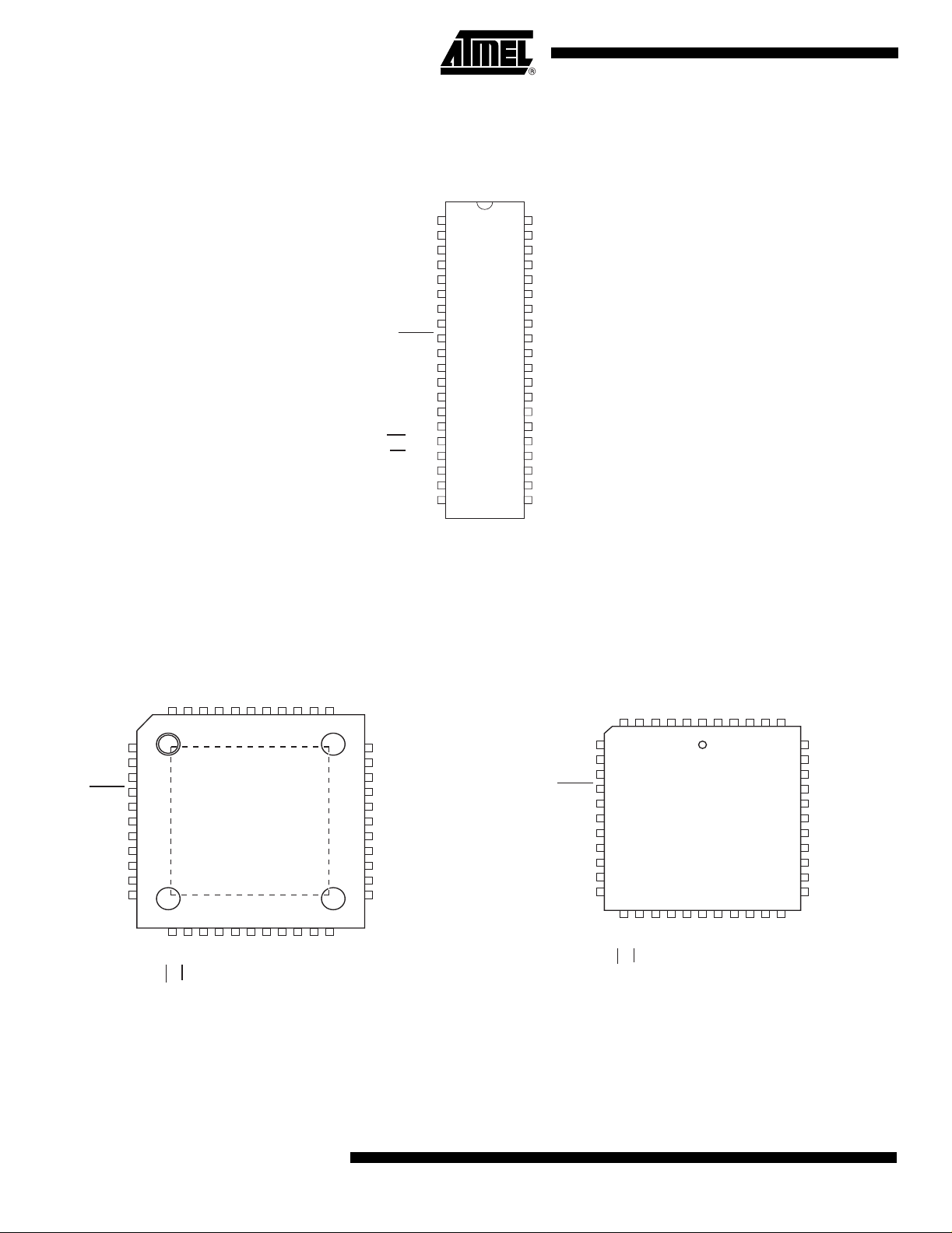
Figure 1. Pinout ATmega8515
PDIP
TQFP/MLF
(OC0/T0) PB0
(T1) PB1
(AIN0) PB2
(AIN1) PB3
(SS) PB4
(MOSI) PB5
(MISO) PB6
(SCK) PB7
RESET
(RXD) PD0
(TDX) PD1
(INT0) PD2
(INT1) PD3
(XCK) PD4
(OC1A) PD5
(WR) PD6
(RD) PD7
XTAL2
XTAL1
GND
1
2
3
4
5
6
7
8
9
10
11
12
13
14
15
16
17
18
19
20
40
VCC
39
PA0 (AD0)
38
PA1 (AD1)
37
PA2 (AD2)
36
PA3 (AD3)
35
PA4 (AD4)
34
PA5 (AD5)
33
PA6 (AD6)
32
PA7 (AD7)
31
PE0 (ICP/INT2)
30
PE1 (ALE)
29
PE2 (OC1B)
28
PC7 (A15)
27
PC6 (A14)
26
PC5 (A13)
25
PC4 (A12)
24
PC3 (A11)
23
PC2 (A10)
22
PC1 (A9)
21
PC0 (A8)
PLCC
(MOSI) PB5
(MISO) PB6
(SCK) PB7
RESET
(RXD) PD0
NC*
(TXD) PD1
(INT0) PD2
(INT1) PD3
(XCK) PD4
(OC1A) PD5
PB4 (SS)
PB3 (AIN1)
PB2 (AIN0)
PB1 (T1)
PB0 (OC0/T0)
NC*
4443424140393837363534
1
2
3
4
5
6
7
8
9
10
11
1213141516171819202122
NC*
GND
XTAL2
XTAL1
(RD) PD7
(WR) PD6
VCC
PA0 (AD0)
PA1 (AD1)
(A8) PC0
(A9) PC1
(A10) PC2
PA2 (AD2)
PA3 (AD3)
33
32
31
30
29
28
27
26
25
24
23
(A11) PC3
(A12) PC4
NC*
7
8
9
10
11
12
13
14
15
16
17
PA4 (AD4)
PA5 (AD5)
PA6 (AD6)
PA7 (AD7)
PE0 (ICP/INT2)
NC*
PE1 (ALE)
PE2 (OC1B)
PC7 (A15)
PC6 (A14)
PC5 (A13)
NOTES:
1. MLF bottom pad should be soldered to ground.
2. * NC = Do not connect
(MOSI) PB5
(MISO) PB6
(SCK) PB7
RESET
(RXD) PD0
(TXD) PD1
(INT0) PD2
(INT1) PD3
(XCK) PD4
(OC1A) PD5
be used in future devices
PB4 (SS)
PB3 (AIN1)
PB2 (AIN0)
PB1 (T1)
PB0 (OC0/T0)
NC*
VCC
PA0 (AD0)
PA1 (AD1)
PA2 (AD2)
65432
1
4443424140
1819202122232425262728
NC*
GND
XTAL2
(RD) PD7
(WR) PD6
XTAL1
(A8) PC0
(A9) PC1
(A10) PC2
(A11) PC3
PA3 (AD3)
39
PA4 (AD4)
38
PA5 (AD5)
37
PA6 (AD6)
36
PA7 (AD7)
35
PE0 (ICP/INT2)
34
NC*
33
PE1 (ALE)
32
PE2 (OC1B)
31
PC7 (A15)
30
PC6 (A14)
29
PC5 (A13)
(A12) PC4
2
ATmega8515(L)
2512F–AVR–12/03
Page 3
ATmega8515(L)
Overview The ATmega8515 is a low-powe r CMOS 8-bit microcontroller base d on the AVR
enhanced RISC architecture. By executing powerful instructions in a single clock cycle,
the ATmega8515 achieves throughputs approaching 1 MIPS per MHz allowing the system designer to optimize power consumption versus processing speed.
Block Diagram Figure 2. Block Diagram
VCC
PA0 - PA7 PC0 - PC7
PORTA DRIVERS/BUFFERS
PE0 - PE2
PORTE
DRIVERS/
BUFFERS
PORTC DRIVERS/BUFFERS
GND
PORTA DIGITAL INTERFACE
PROGRAM
COUNTER
PROGRAM
FLASH
INSTRUCTION
REGISTER
INSTRUCTION
DECODER
CONTROL
LINES
AVR CPU
PROGRAMMING
LOGIC
STACK
POINTER
SRAM
GENERAL
PURPOSE
REGISTERS
X
Y
Z
ALU
STATUS
REGISTER
SPI
PORTE
DIGITAL
INTERFACE
PORTC DIGITAL INTERFACE
TIMERS/
COUNTERS
INTERNAL
OSCILLATOR
WATCHDOG
TIMER
MCU CTRL.
& TIMING
INTERRUPT
UNIT
EEPROM
USART
OSCILLATOR
INTERNAL
CALIBRATED
OSCILLATOR
XTAL1
XTAL2
RESET
2512F–AVR–12/03
+
-
PORTB DIGITAL INTERFACE
PORTB DRIVERS/BUFFERS
COMP.
INTERFACE
PORTD DIGITAL INTERFACE
PORTD DRIVERS/BUFFERS
PD0 - PD7PB0 - PB7
3
Page 4

The AVR core combines a ric h instr uctio n set wit h 32 general purpose worki ng regi sters .
All the 32 regi sters are dire ctly conn ected to the Arithm etic Logic U nit (A LU), all owing
two independent regist ers t o be acces sed i n one sing le inst ructi on execut ed in one clo ck
cycle. The resulting arc hitect ur e is more code eff icient whil e achievi ng throug hput s up to
ten times faster than conventional CISC microcontrollers.
The ATmega8515 provides the foll owing featur es: 8K bytes of In-Sy stem Progra mmable
Flash with Read-While-Write capabilities, 512 bytes EEPROM, 512 bytes SRAM, an
External memory interfa ce, 35 genera l purpose I/O lines, 32 ge neral purpo se working
registers, two flexible Timer/Counters with compare modes, Internal and External interrupts, a Serial Prog rammabl e U SART, a pr ogramma ble Watch dog T imer w ith in ternal
Oscillator, a SPI se rial port, and three s oft ware sel ectabl e power saving modes . The Idl e
mode stops the CPU while allowing the SRAM, Timer/Counters, SPI port, and Interrupt
system to continue functioning. The Power-down mode saves the Register contents but
freezes the Oscillator, disab ling all other chip f unctions unt il the ne xt interrupt or ha rdware reset. In St andby mode, the crystal/resonator Oscillator is running while the rest of
the device is sleeping. This allows very fast start-up combined with low-power
consumption.
The device is manufactured using Atmel’s high density nonvolatile memory technology.
The On-chip ISP Flash allows the Program memory to be reprogrammed In-System
through an SPI serial interf ace, by a convent ional nonvol atile memory p rogrammer, or
by an On-chip Boot program running on the AVR core. The boot program can u se any
interface to download the application program in the Application Flash memory. Software in the Boot Flash section will continue to run while the Application Flash section is
updated, providing true Read-While-Write operation. By combining an 8-bit RISC C PU
with In-System Self-programmable Flash on a monolithic chip, the Atmel ATmega8515
is a powerful microcontroller that provides a highly flexible and cost effective solution to
many embedded control applications.
The ATmega8515 is supported with a full suite of program and system development
tools including: C Com pilers, M acro assembl ers, Program debugge r/simulators, In-circuit Emulators, and Evaluation kits.
Disclaimer Typical values contained i n this dat asheet are based on simulatio ns and ch aracteriza-
tion of other AVR microcontrollers manufactured on the same process technology. Min
and Max values will be available after the device is characterized.
AT90S4414/8515 and ATmega8515 Compatibility
A T90S4414/8515 Compatibility Mode
The ATmega8515 provides all the features of the AT90S4414/8515. In addition, several
new features are added. The ATmeg a8515 is backward compatible with
AT90S4414/8515 in most c ases. However, some inco mpatibilities be tween the two
microcontrollers exist. To solve this problem, an AT90S4414/8515 com patibility mode
can be selected by programming the S8515C Fuse. ATmega8515 is 100% pin compatible with AT90S4414/8515, and can replace the AT90S4414/8515 on current printed
circuit boards. However, the location of Fuse bits and the electrical characteris tics differs between the two devices.
Programming the S8515C Fuse will change the following functi onality:
• The timed sequence for changing the Watchdog Time-out period i s disabled. See
“Timed Sequences for Changing t he Configurat ion of the Watchdog Timer” on page
52 for details .
• The double buffering of the USART Receive Registers is disabl ed. See “AVR
USART vs. AVR UART – Compatibility” on page 135 for details.
• PORTE(2:1) will be set as output, and PORTE0 will be set as input.
4
ATmega8515(L)
2512F–AVR–12/03
Page 5

ATmega8515(L)
Pin Descriptions
VCC Digital supply voltage. GND Ground. Port A (PA7..PA0) Port A is an 8-bit bi-directional I/O port with internal pull-up resistors (selected for each
bit). The Port A output buf fers have symmetrical drive char acteristics with both high sink
and source capability. When pins PA0 to PA7 are used as inputs and are externally
pulled low, they will source current if the internal pull-u p resistors are activated. The Por t
A pins are tri-stated when a reset condition becomes active, even if the clock is not
running.
Port A also serves the functions of vario us special features of the ATmega8515 as listed
on page 66.
Port B (PB7..PB0) Port B is an 8-bit bi-directional I/O port with internal pull-up resistors (selected for each
bit). The Port B output buf fers have symmetrical drive char acteristics with both high sink
and source capability. As inputs, Por t B pins that are externally p ulled low w ill source
current if the pull-up resistors are activated. The Port B pins are tri-stated when a reset
condition becomes active, even if the clock is not running.
Port B also serves the functions of vario us special features of the ATmega8515 as listed
on page 66.
Port C (PC7..PC0) Port C is an 8-bit bi-directional I/O port with internal pull-up resistors (selected for each
bit). The Port C output buffers have symmetri cal drive character ist ics with both high sink
and source capability. As inputs, Port C pins that are externally pulled low will source
current if the pull-up resistors are activated. The Port C pins are tri-stated when a reset
condition becomes active, even if the clock is not running.
Port D (PD7..PD0) Port D is an 8-bit bi-directional I/O port with internal pull-up resistors (selected for each
bit). The Port D output buffers have symmetri cal drive character ist ics with both high sink
and source capability. As inputs, Port D pins that are externally pulled low will source
current if the pull-up resistors are activated. The Port D pins are tri-stated when a reset
condition becomes active, even if the clock is not running.
Port D also serves the functi ons of vari ous spe cial featu res of the ATmega85 15 as list ed
on page 71.
Port E(PE2..PE0) Port E is an 3-bit bi-directional I/O port with internal pull-up resistors (selected for each
bit). The Port E output buf fers have symmetrical drive char acteristics with both high sink
and source capability. As inputs, Por t E pins that are externally p ulled low w ill source
current if the pull-up resistors are activated. The Port E pins are tri-stated when a reset
condition becomes active, even if the clock is not running.
Port E also serves the functions of vario us special features of the ATmega8515 as listed
on page 73.
RESET
XTAL1 Input to the inverting Osci ll ator amplifier and input to the internal clock operating circuit. XTAL2 Output from the inverting Oscillator amplifier.
2512F–AVR–12/03
Reset input. A low level on this pin for longer than the minimum pulse length will generate a reset, even if the clock is not running. The minimum pulse length is given in Table
18 on page 45. Shorter pulses are not guara nteed to generate a reset.
5
Page 6

About Code Examples
This documentation contai ns simpl e code examples that bri efly show how to use var ious
parts of the device. These cod e example s assume tha t the part speci fic header file is
included before compilation. Be aware that not all C Compiler vendors include bit definitions in the header files and interrupt handling in C is compiler dependent. Please
confirm with the C Compiler documentation for more det ails.
6
ATmega8515(L)
2512F–AVR–12/03
Page 7
ATmega8515(L)
AVR CPU Core
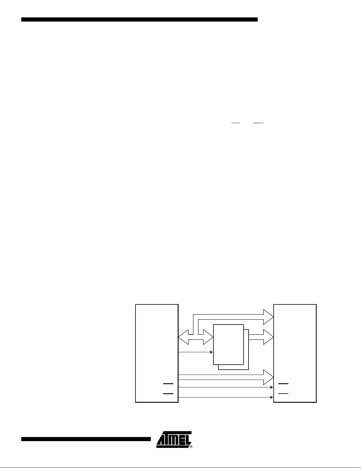
Introduction This section discusses the AV R core architecture in general. The main function of the
CPU core is to e nsu re corre ct program exec ution. The CP U mu st there fore b e abl e to
access memories, perform cal culations, control peripher als, and handle interrupts.
Architectural Overview Figure 3. Block Diagram of the AVR Architecture
Data Bus 8-bit
Flash
Program
Memory
Instruction
Register
Instruction
Decoder
Control Lines
Program
Counter
Direct Addressing
Status
and Control
32 x 8
General
Purpose
Registrers
ALU
Indirect Addressing
Data
SRAM
EEPROM
Interrupt
Unit
SPI
Unit
Watchdog
Timer
Analog
Comparator
I/O Module1
I/O Module 2
I/O Module n
2512F–AVR–12/03
I/O Lines
In order to maximize per formance and parallelism, the AVR uses a Harvard architecture
– with separate memories and buses for program and data. Instructions in the Program
memory are executed with a single level pipelining. While one instruction is being executed, the next instruction is pre-fetched from the Program memory. This concept
enables in struc tions to be exec uted in ever y clock cy cle. Th e Progr am mem ory is I nSystem re programmable Flash memory.
The fast-access Regist er File contains 32 x 8-bit general purpose working registers with
a single clock cycle a ccess time. This a llows single -cycle Arithmetic Logic Unit (ALU)
operation. In a typical AL U operation, two operands are out put from the Registe r File,
the operation is executed, and the result is stored back in the Register File – in one
clock cycle.
7
Page 8

Six of the 32 registers can be used as three 16-bit indirect address register pointers for
Data Space addressing – enabling efficient address calculations. One of the these
address pointers can also be used as an address pointer for loo k up tables in Flash Program memory. These adde d function registers are the 1 6-bit X-, Y-, and Z-register,
described later in t his section.
The ALU supports arithmetic and logic operations between registers or between a constant and a register. Single register operations can also be executed in the ALU. After
an arithmetic operation, the St atus Regist er is updat ed to reflect i nformation a bout the
result of the operation.
Program flow is provided by conditional and unconditional jump and call instructions,
able to directly address the whole address space. Most AVR instructions have a single
16-bit word format. Every Program memory address contains a 16- or 32-bit instruction.
Program Flash memory space is divided in two sections, the Boot Program section and
the Application Program secti on. Both sections hav e dedicated Lock bits for write and
read/write protect ion. The SPM instruction that writ es into the Application Flash memory
section must reside in the Boot Program section.
During interrupts and subroutine cal ls, the return address Program Counter (PC) is
stored on the Stack . Th e Stac k is effectiv ely al locat ed in t he general data SRAM , a nd
consequently the Stack size is only limited by the total SRAM size and the usage of the
SRAM. All user programs must initialize the SP in the reset routine (before subroutines
or interrupts are executed). The Stack Pointer SP is read/write accessible in the I/O
space. The data SRAM can easily be accessed through the five different addressing
modes supported in the AVR architecture.
ALU – Arithmetic Logic Unit
The memory spaces in the AVR architecture are all linear and regular memory maps.
A flexible interrupt module has its Control Registers in the I/O space with an additional
Global Interrupt Enable bit in the Status Registe r. All interrupts have a separat e interrupt
vector in the Interrupt Vector table. The interrupts have priority in accordance with their
Interrupt Vector pos ition. The lower the Interrupt Vect or address, the higher the priorit y.
The I/O memory space contains 64 addresses for CPU peripheral functions as Control
Registers, SPI, and other I/O functions. The I/O Memory can be accessed directly, or as
the Data Space locations follo wing those of the Register File, $20 - $5F.
The high-performance AVR ALU operates in direct connection with all the 32 general
purpose worki ng register s. Withi n a single cl ock cycle, arithmet ic operat ions betw een
general purp ose regis ters or be tween a re giste r and an imme diate ar e ex ecuted . T he
ALU operations are divided i nto three main categories – ari thmet ic, logical, and bit-functions. Some implementations of the architecture also provide a powerful multiplier
supporting both signed/unsi gned m ultiplic ation and fractio nal format. See the “Ins truction Set” section for a detailed description.
8
ATmega8515(L)
2512F–AVR–12/03
Page 9

ATmega8515(L)
Status Register The Status Register contains information about the result of the most recently executed
arithmetic instruction. This information can be used for altering program flow in order to
perform conditi onal opera tions. Note that the Stat us Registe r is update d after all AL U
operations, as specified in the Instruction Set Reference. This will in many cases
remove the need for using the dedicated compare instructions, resulting in faster and
more compact code.
The Status Register is not a utomaticall y stored wh en ent ering an i nterrupt routine and
restored when returning from an interrupt. This must be handled by software.
The AVR Status Register – SREG – is defined as:
Bit 76543210
ITHSVNZCSREG
Read/Write R/W R/W R/W R/W R/W R/W R/W R/W
Initial Value00000000
• Bit 7 – I: Glob a l In te r ru p t En a bl e
The Global Interrupt Enable bit must be set for the interrupts to be enabled. The individual interrupt enable cont rol i s then pe rf ormed in se parat e Contro l Reg isters. I f the Global
Interrupt Enable Register is cleared, none of the interrupts are enabled independent of
the individual interrupt enable sett ings. The I-bit is cl eared by hardwar e after an in terrup t
has occurred, and is set by the RETI instruction to enable subsequent interrupts. The Ibit can also be set and cleared by the application with the SEI and CLI instructions, as
described in the instruction set reference.
• Bit 6 – T: Bit Copy Storage
The Bit Copy instructions BLD (Bit LoaD) and BST (Bit STore) use the T-bit as sour ce or
destination for the operated bit. A bit from a register in the Reg ister File can be copied
into T by the BST instruction, and a bit i n T can be copied into a b it in a reg ister in the
Register File by the BLD instruct ion.
• Bit 5 – H: Half Car ry Flag
The Half Carry Fl ag H indicates a Hal f Carry in some ari thmetic operations. Half Carry is
useful in BCD arithmetic. See the “Instru cti on Set Description” for detailed information.
• Bit 4 – S: Sign Bit, S = N
⊕ V
The S-bit is always an exclusiv e or between t he Negative Flag N and the Two’ s Complement Overflow Flag V. See the “Instruction Set Descr iption” for detailed information.
• Bit 3 – V: Two’s Complement O ve r fl ow F lag
The Two’s C omplem ent O verflow Fla g V s upports two’s compl eme nt a rithmet ics. S ee
the “Instruction Set Descr iption” for detailed information.
• Bit 2 – N: N e gative F lag
The Negative Flag N indicates a negative result in an arithmetic or logic operation. See
the “Instruction Set Descr iption” for detailed information.
• Bit 1 – Z: Zero Flag
The Zero Flag Z indicates a zero result i n an arith metic or logic operation. S ee the
“Instruction Set Description” for detailed information.
• Bit 0 – C: Carry Flag
2512F–AVR–12/03
The Carry Flag C indicates a carry in an arithmetic or logic operation. See the “Instruction Set Description” for detailed information.
9
Page 10

General Purpose Register File
The Register F ile is optim ized f or the A VR E nhanc ed RIS C in struction set. I n orde r to
achieve the required performance and flexibility, the following input/output schemes are
supported by the Register File:
• One 8-bit output operand and one 8-bit result input
• Two 8-bit output operands and one 8-bit result input
• Two 8-bit output operands and one 16-bit resu lt input
• One 16-bit output operand and one 16-bit result input
Figure 4 shows the structure of the 32 general purpose working registers in the CPU.
Figure 4. AVR CPU General Purpose Working Registers
70Addr.
R0 $00
R1 $01
R2 $02
…
R13 $0D
General R14 $0E
Purpose R15 $0F
Working R16 $10
Registers R17 $11
…
R26 $1A X-register Low Byte
R27 $1B X-register High Byte
R28 $1C Y-register Low Byte
R29 $1D Y-register High Byte
R30 $1E Z-register Low Byte
R31 $1F Z-register High Byte
Most of the instruction s operati ng on the Regist er File have di rec t access to al l regi sters ,
and most of them are single cycle instructions.
As shown in Figure 4, each register is also assigned a Data memory address, mapping
them directly into the first 32 locati ons of the user Data Space. Although not being physically implemented as SRAM locations, t his memory organizati on provides great
flexibility in access of the registers, as the X-, Y-, and Z-pointer Registers can be set to
index any register in the file.
10
ATmega8515(L)
2512F–AVR–12/03
Page 11
ATmega8515(L)
The X-register, Y-register, and Z-register
The registers R26..R31 have some added functions to their general purpose usage.
These registers are 16-bit address pointers for i ndirect addressing of the Data Sp ace.
The three indirect address registers X, Y, and Z are defined as described in Figure 5.
Figure 5. The X-, Y-, and Z-registers
15 XH XL 0
X-register 7 0 7 0
R27 ($1B ) R26 ($1A )
15 YH YL 0
Y-register 7 0 7 0
R29 ($1D ) R28 ($1C)
15 ZH ZL 0
Z-register 7 0 7 0
R31 ($1F ) R30 ( $1E)
In the different addressi ng mode s these ad dress registe rs have f unctions as f ixed di splacement, automatic increm ent, and autom atic decremen t (see the Inst ruction Set
reference for details).
Stack Pointer The Stack is mainly used for storing temp orary data, for storing l ocal variables and for
storing return addresses after interrupts and subroutine calls. The Stack Pointer Register always points to the top of the Stack. Note that the Stack is implemented as growing
from higher memory locati ons to lower mem ory locations. This implies that a Stack
PUSH command decreases the Stack Pointer.
The Stack Pointer points to the data SRAM Stack area where the Subroutine and Interrupt Stacks are located. This Stack space in the data SRAM must be defined by the
program before any subroutine calls are executed or interrupts are enabled. The Stack
Pointer must be set to point above $60. The Stack Pointer is decremented by one when
data is pushed onto the Stack with the PUSH instruction, and it is decremented by two
when the return address is pushed onto the Stack with subroutine call or interrupt. The
Stack Pointer is incremented by one when data is popped from the Stack with the POP
instruction, and it is incremented by two when address is popped from the Stack with
return from subroutine RET or return from interrupt RETI.
The AVR Stack Pointer is implemented as two 8-bit registers in the I/O space. The number of bits actually used i s implementation dependent. Note that the data space in some
implementations of the AVR architecture is so small that only SPL is needed. In this
case, the SPH Register will not be present.
Bit 1514131211109 8
SP15 SP14 SP13 SP12 SP11 SP10 SP9 SP8 SPH
SP7 SP6 SP5 SP4 SP3 SP2 SP1 SP0 SPL
76543210
Read/Write R/W R/W R/W R/W R/W R/W R/W R/W
R/W R/W R/W R/W R/W R/W R/W R/W
Initial Value00000000
00000000
2512F–AVR–12/03
11
Page 12
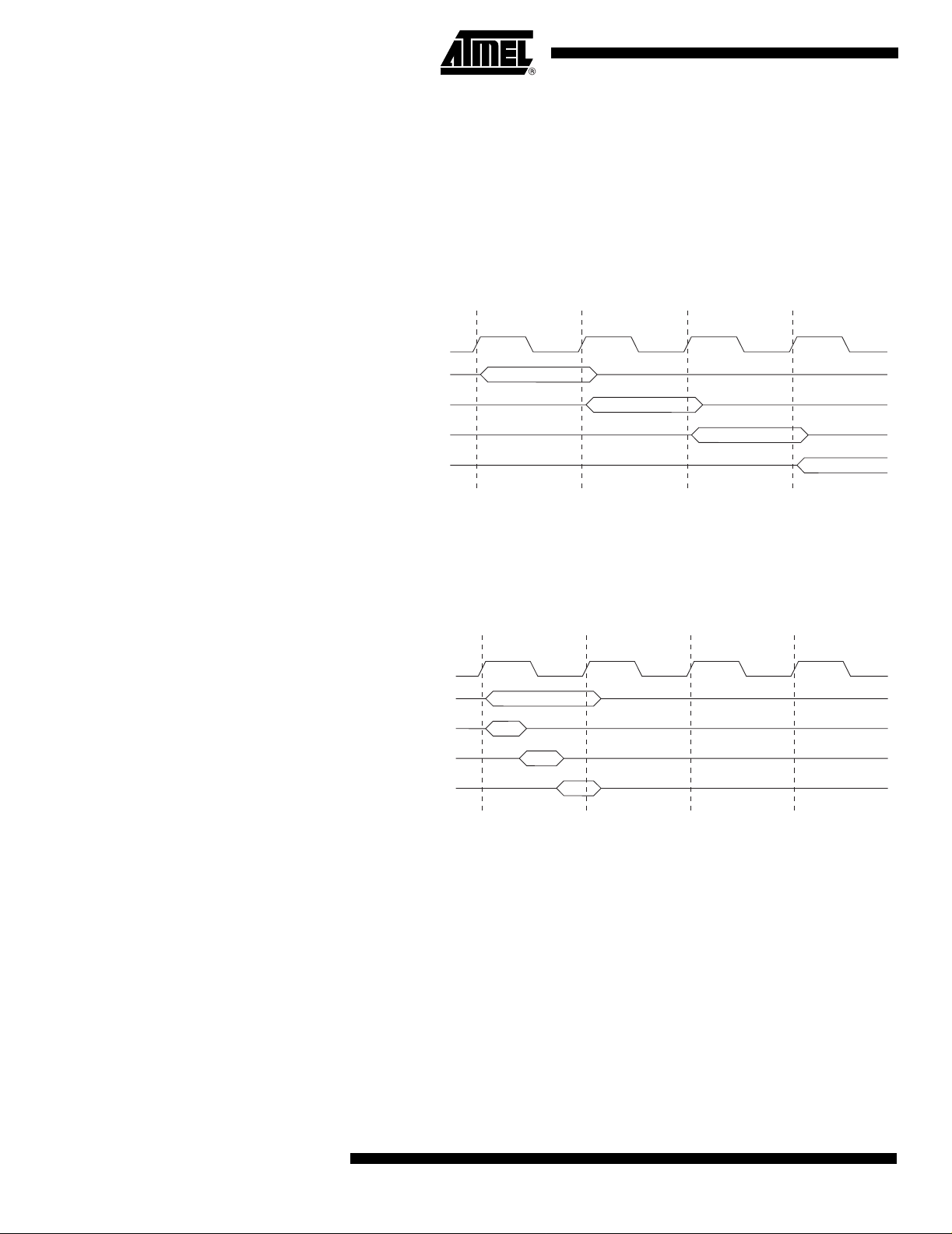
Instruction Execution Timing
This section describes the gener al access timing conc epts for i nstruct ion execut ion. The
AVR CPU is driven by the CPU clock clk
, directly generated from the selected clock
CPU
source for the chip. No internal clock division is used.
Figure 6 shows the parallel instructi on fetches and instruc tion exec utions enab led by the
Harvard architecture and the fast-access Register Fil e concept. This is the basic pipelining concept t o obtain up t o 1 M IPS p er MH z with t he co rrespondin g u nique res ults for
functions per cost, functions per clocks, and functions per power-unit.
Figure 6. The Paral lel Instruction Fetches and Instruction Executions
T1 T2 T3 T4
clk
CPU
1st Instruction Fetch
1st Instruction Execute
2nd Instruction Fetch
2nd Instruction Execute
3rd Instruction Fetch
3rd Instruction Execute
4th Instruction Fetch
Figure 7 shows the internal timing concept for the Register File. In a single clock cycle
an ALU operation using two register operands is executed, and the result is stored back
to the destination regis ter.
Reset and Interrupt Handling
Figure 7. Single Cycle ALU Operat ion
T1 T2 T3 T4
clk
CPU
Total Execution Time
Register Operands Fetch
ALU Operation Execute
Result Write Back
The AVR provides several different interrupt sources. These interrupts and the separate
Reset Vector each have a separate program vecto r in the Program memory space. All
interrupts are assigned indi vidual en able bits w hich must b e wr itten logic one together
with the Global Interru pt Ena ble bit i n the Stat us Reg ister in orde r to enabl e the i nterr upt.
Depending on the Program Counter value, interrupts may be automatically disabled
when Boot Lock bits BLB02 or BLB12 are programmed. This feature improves software
security. See the section “Memor y Programming” on page 177 for details.
The lowest addresse s in the Program memory spa ce are by default define d as the
Reset and Interrupt Vectors. The complete list of vectors is shown in “Interrupts” on
page 53. The list also determines the priority levels of the different interrupts. The lower
the address the higher is the priority l evel. RESET ha s the highe st priority, and next is
INT0 – the External Interrupt Request 0. The Interr upt Vectors can be moved to the star t
of the Boot Flash section by setting the IVSEL bit in the General Int errupt Control Register (GICR). Refer to “Interrupts” on page 53 for more information. The Reset Vector can
12
ATmega8515(L)
2512F–AVR–12/03
Page 13

ATmega8515(L)
also be moved to the start of the Boot Flash section by programming the BOOTRST
Fuse, see “Boot Loader Support – Read-While-Write Self-Programming” on page 164.
When an interrupt occurs, the Global In terrupt Enab le I-bit is cleared and al l interrupts
are disabled. The user softw are ca n wri te logi c on e to the I-bit t o en able n este d int errupts. All enabled interrupts can then i nterrupt the current interrupt routine. The I-bit is
automatically set when a Return from Interrupt instruction – RETI – is executed.
There are basicall y two types of inter rupts. The first type is triggered by an event that
sets the Interrupt Flag. For these interrupts, the Program Counter is vectored to the
actual Interrupt Vector in order to execute the interrupt handling routine, and hardware
clears the corresponding Interrupt Flag. Interrupt Flags can also be cleared by writing a
logic one to the flag bi t posi tion( s) to be c leared. If an i nterr upt condi tion oc cur s while the
corresponding Interrupt Enable bit is cleared, the Interrupt Flag will be set and remembered until the interrupt is enabled, or the flag is cleared by software. Similarly, if one or
more interrupt conditions occur while the Global Interrupt Enable bit is cleared, the corresponding interrupt flag(s) will be set and remembered until th e Global Interrupt Enable
bit is set, and will then be executed by order of pri ority.
The second type of interrupts will trigger as long as the interrupt condition is present.
These interrupts do not necessarily have Interrupt Flags. If the interrupt condition disappears before the interrupt is enabled, the interrupt will not be tri ggered.
When the AVR exits from an interrupt, it will always return to the main pr ogram and execute one more instruction before any pending interrupt is served.
Note that the Status Register is not automatically stored when entering an interrupt routine, nor restored when returning from an interrupt routine. This must be handled by
software.
When using the CLI instruction to disable interrupts, the interrupts will be immediately
disabled. No interrupt will be executed after the CLI instruction, even if it occurs simultaneously with the CLI instruction. The following example shows how this can be used to
avoid int errupts during the timed EEPROM write sequence..
Assembly Code Example
in r16, SREG ; store SREG value
cli ; disable interrupts during timed sequence
sbi EECR, EEMWE ; start EEPROM write
sbi EECR, EEWE
out SREG, r16 ; restore SREG value (I-bit)
C Code Example
char cSREG;
cSREG = SREG; /* store SREG value */
/* disable interrupts during timed sequence */
_CLI();
EECR |= (1<<EEMWE); /* start EEPROM write */
EECR |= (1<<EEWE);
SREG = cSREG; /* restore SREG value (I-bit) */
2512F–AVR–12/03
13
Page 14

When using the SEI instruction to enable interrupts, the instruction following SEI will be
executed before any pending inter rupt s, as shown in this example.
Assembly Code Example
sei ; set global interrupt enable
sleep; enter sleep, waiting for interrupt
; note: will enter sleep before any pending
; interrupt(s)
C Code Example
_SEI(); /* set global interrupt enable */
_SLEEP(); /* enter sleep, waiting for interrupt */
/* note: will enter sleep before any pending interrupt(s) */
Interrupt Response Time The interrupt execution response for all the enabled AVR interrupts is four clock cycles
minimum. After four clock cycles the Program Vector address for the actual interrupt
handling routine is executed. During this f our clock cycle period, the Program Counter is
pushed onto the Stack. Th e Vector is n ormally a jum p to the interrupt routine, and this
jump takes three clock cycles. If an interrupt occurs during execution of a multi-cycle
instruction, this instruction is completed before the interrupt is served. If an interrupt
occurs when the MCU is in sleep mode, the interrupt execution response time is
increased by four clock cycles. This increase comes in additio n to the st art-up time from
the selected sleep mode.
A return from an interrupt handling routine takes four clock cycles. During these four
clock cycles, t he Program Counter (two bytes) is popped back from the St ack, the Stack
Pointer is incremented by two, and the I-bit in SREG is set.
14
ATmega8515(L)
2512F–AVR–12/03
Page 15

ATmega8515(L)
AVR ATmega8515 Memories
In-System Reprogramma ble Flash Program memory
This section describes the different memories in the ATm ega8515. The AVR archit ecture has two main memory spaces, the Data Memory and the Program memory space.
In addition, the ATmega8515 features an EEPROM Mem ory for data storage. All three
memory spaces are linear and regul ar.
The ATmega8515 contains 8K bytes On-chip In-System Reprogrammable Flash memory for program storage. Since all AVR instructions are 16 or 32 bits wide, the Flash is
organized as 4K x 16. For software security, the Flash Program memory space is
divided into two sections, Boot Program section and Application Program section.
The Flash me mory has an endurance of at least 10 ,000 write/erase cycles. The
ATmega8515 Program Cou nter (PC) is 1 2 bits wi de, th us add ressing the 4K Progra m
memory locations. The operation of Boot Program section and associated Boot Lock
bits for software protection are described in detail in “Boot Loader Support – ReadWhile-Write Self-Pr ogramming” on page 164. “Memory Programming” on page 177 contains a detailed description on Flash data serial downloading using the SPI pins.
Constant tables can be allocated within the entire Program memory address space, see
the LPM – Load Program memory instruction description.
Timing diagrams for instruction fetch and execution are presented in “Instruction Execution Timing” on page 12.
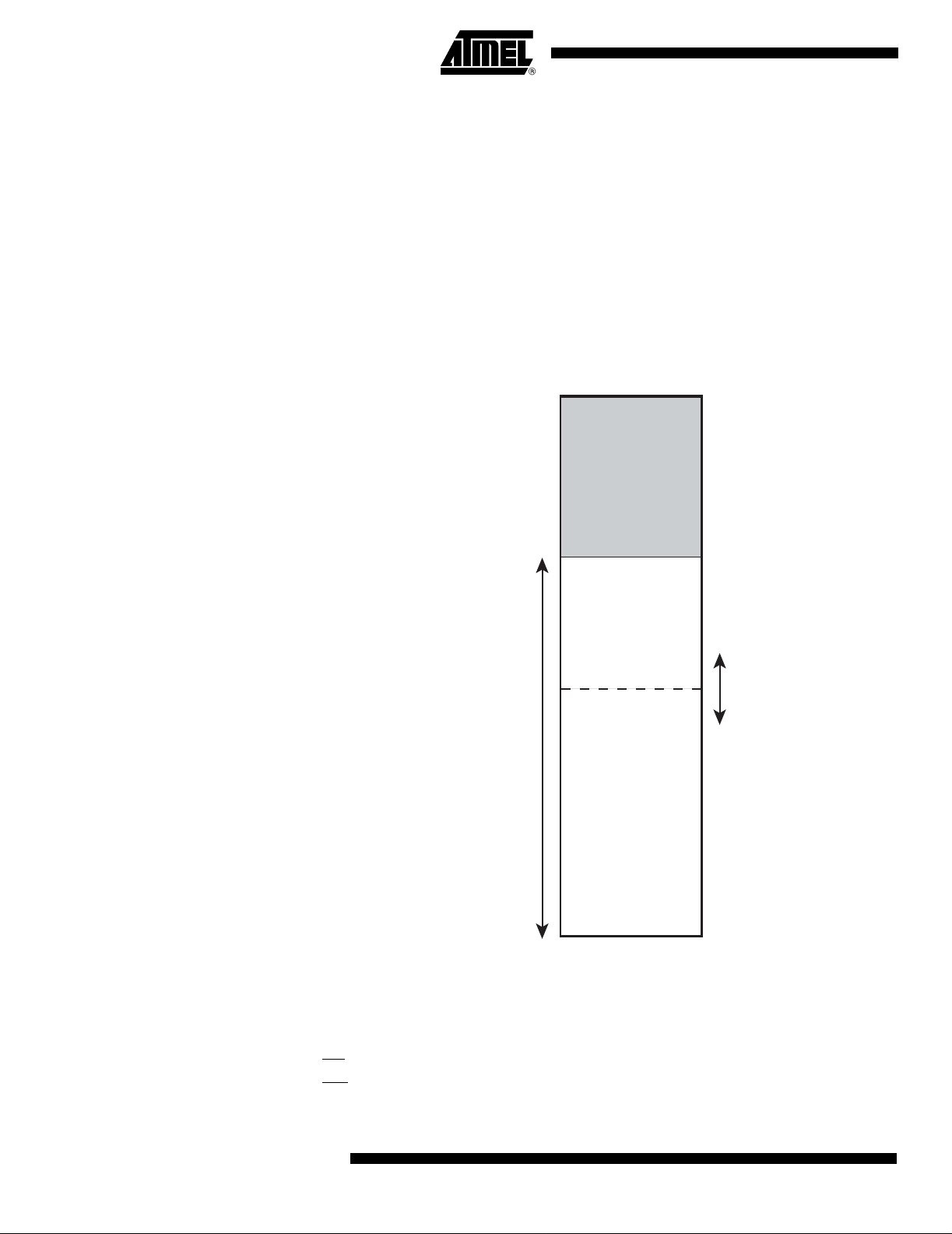
Figure 8. Program memory Map
Application Flash Section
Boot Flash Section
$000
$FFF
2512F–AVR–12/03
15
Page 16

SRAM Data Memory Figure 9 shows how the ATmega8515 SRAM Memory is organized.
The lower 608 Data Me mory loc ations address the Regi ster File, the I/O Mem ory, and
the internal data SRAM. The first 96 locations ad dress the R egister File and I /O Memory, and the next 512 locations address the internal data SRAM.
An optional external data SRAM can be used with the ATmega8515. This SRAM will
occupy an area in the remaining address locations in the 64K address space. This area
starts at the address following the internal SRAM. The Register File, I/O, Extended I/O
and Internal SRAM occu pies the lowest 608 bytes i n normal mode, so when using 64KB
(65536 bytes) of External Memory, 64928 Bytes of External Memory are available. See
“External Memory Interface” on page 24 for details on how to take advantage of the
external memory map.
When the addresses accessing the SRAM memory space exceeds the internal Data
memory locations, the external data SRAM is accessed using the same instructions as
for the internal Data mem ory access. W hen the internal d ata mem ories are acce ssed,
the read and write strobe pins (PD7 and PD6) are inactive during the whole access
cycle. External SRAM operation is enabled by setting the SRE bit in the MCUCR
Register.
Accessing external SRAM takes one additional clock cycl e per byte compar ed to acce ss
of the internal SRAM. This means that the commands LD, ST, LD S, STS, LDD, STD,
PUSH, and POP take one additional clock cycle. If the Stack is placed in external
SRAM, interrupts, subrou tine cal ls and r eturn s take t hre e clock cy cles ext ra because t he
two-byte Progra m Counte r is pushed and po pped, and external me mory acce ss does
not take advantage of the interna l pipe-line memory access. When external SRAM interface is used with wait-stat e, one-byt e external acces s takes two, three, or fo ur additional
clock cycles for one, two, and three wait-states respectively. Interrupts, subroutine calls
and returns will need five, seven, or nine clock cycles more than specified in the i nstruction set manual for one, two, and three wait-states.
The five different addressing modes for the Data memory cover: Direct, Indirect with
Displacement, Indirect , Indi rect with Pre- decr ement, and Indir ect wit h Post-i ncre ment. In
the Register File, registers R26 to R31 feature the indirect addressing pointer registers.
The direct addressing rea ches the entire data space.
The Indirect with Displacement mode reaches 63 address locations from the base
address given by the Y- or Z-register.
When using register indirect addressing modes with automatic pre-decrement and post-
increment, the address regis ter s X, Y, and Z are decremented or incremented.
The 32 general purpose working registers, 64 I/O Registers, and the 512 bytes of inter-
nal data SRAM in the ATmega8515 are all accessible through all these addressing
modes. The Register File is described in “General Purpose Register File” on page 10.
16
ATmega8515(L)
2512F–AVR–12/03
Page 17
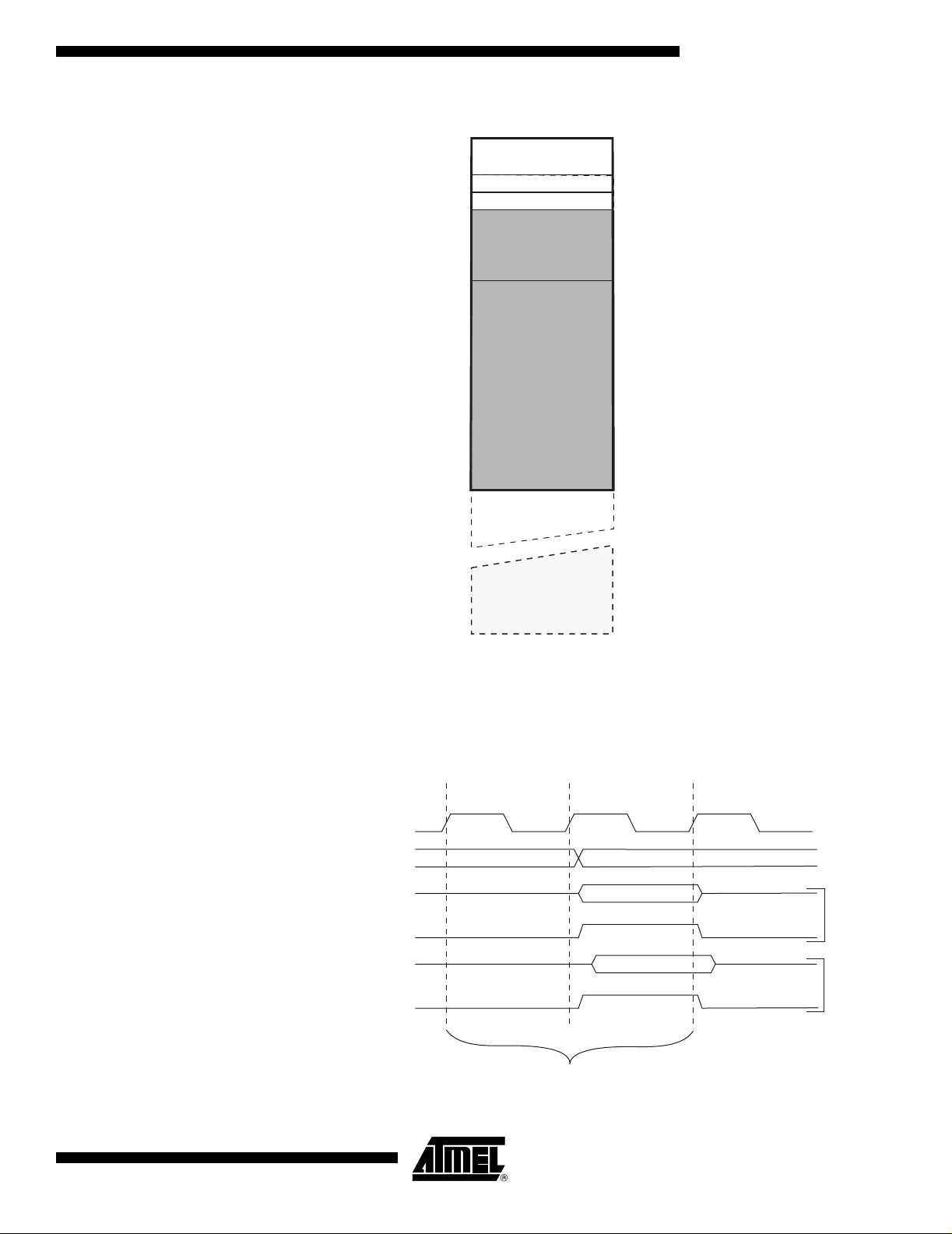
Figure 9. Data Memory Map
ATmega8515(L)
Data Memory
32 Registers
64 I/O Registers
Internal SRAM
(512 x 8)
External SRAM
(0 - 64K x 8)
$0000 - $001F
$0020 - $005F
$0060
$025F
$0260
$FFFF
Data Memory Access Times This section describes the general access timing concepts for internal memory access.
The internal data SRAM access is performed in two clk
cycles as described in Figure
CPU
10.
Figure 10. On-chip Data SRAM Access Cycles
T1 T2 T3
clk
CPU
Address
Compute Address
Address Valid
Data
WR
Write
Data
RD
Memory Access Instruction
Next Instruction
Read
2512F–AVR–12/03
17
Page 18

EEPROM Data Memory The ATmega8515 contains 512 bytes of data EEPROM memory. It is organized as a
separate data space, in which single bytes can be read and written. The EEPROM has
an endurance of at l east 100,000 write/erase cycles. The access between the EEPROM
and the CPU is described in the following, specifying the EEPROM Address Registers,
the EEPROM Data Register, and the EEPROM Control Register.
“Memory Programming” on page 177 contains a detailed description on EEPROM Programming in SPI or Parallel Programming mode.
EEPROM Read/Write Access The EEPROM Access Registers are accessible in the I/O space.
The write access time for the EEPROM is given in Table 1. A self-timing function, however, lets the us er softw are detec t wh en the n ext b yte can be written. If the u ser code
contains instructions that write the EEPROM, some precautions must be taken. In
heavily filtered power supplies, V
causes the device for some period of time to run at a voltage lower than specified as
minimum for the clock frequency used. See “Preventing EEPROM Corruption” on page
23. for details on how to avoid problems in these si tuations.
In order to prevent unintenti onal EEPROM writes, a specific wr ite pro cedure must be f ol-
lowed. Refer to the description of the EEPROM Control Register for details on this.
When the EEPROM is read, the CPU i s halted for four clock cycles before the next
instruction is execut ed. Wh en the E EPRO M is w ritten, the CPU is h alted fo r two cl ock
cycles before the next instr u ction is executed.
is likely to rise or fal l slowly on Power-up/down. Thi s
CC
The EEPROM Address Register – EEARH and EEARL
Bit 151413121110 9 8
–––––––EEAR8EEARH
EEAR7 EEAR6 EEAR5 EEAR4 EEAR3 EEAR2 EEAR1 EEAR0 EEARL
76543210
Read/Write R R R R R R R R/W
R/W R/W R/W R/W R/W R/W R/W R/W
Initial Value0000000X
XXXXXXXX
• Bits 15..9 – Res: Reserved Bits
These bits are reserved bit s in t he ATmega8515 and will always read as zero.
• Bits 8..0 – EEAR8..0: EEPROM Address
The EEPROM Ad dress Registers – EEAR H and EEARL – speci fy the EEPROM
address in the 512 bytes EEPROM space. The EEPROM data bytes are addressed linearly between 0 and 511. The ini tial val ue o f EEAR is undefi ned. A proper value must be
written before the EEPROM may be accessed.
18
ATmega8515(L)
2512F–AVR–12/03
Page 19

ATmega8515(L)
The EEPROM Data Register – EEDR
The EEPROM Control Regi ster – EECR
Bit 76543210
MSB LSB EEDR
Read/Write R/W R/W R/W R/W R/W R/W R/W R/W
Initial Value00000000
• Bits 7..0 – EEDR7.0: EEPROM Data
For the EEPROM write operation, the EEDR Register contains the data to be written to
the EEPROM in the address given by the EEAR Register. For the EEPROM read operation, the EEDR contains the data read out from the EEPROM at the address given by
EEAR.
Bit 76543210
– – – – EERIE EEMWE EEWE EERE EECR
Read/Write R R R R R/W R/W R/W R/W
Initial Value 0 0 0 0 0 0 X 0
• Bits 7..4 – Res: Reserved Bits
These bits are reserved bit s in t he ATmega8515 and will always read as zero.
• Bit 3 – EERIE: EEPROM Ready Interrupt Enable
Writing EERIE to one enables the EEPROM Ready Interrupt if the I-bit in SREG is set.
Writing EERIE to zero disables the interrupt. The EEPROM Re ady interrupt generates a
constant interrupt when EEWE is cleared.
• Bit 2 – EEMWE: EEPROM Master Write Enable
The EEMWE bit determines wh ether setting E EWE to one causes the EEP ROM to be
written. When EEMWE is set, setting EEWE within four clock cyc les will write data to the
EEPROM at the selected address If EEMWE is zero, setting EEWE will have no effect.
When EEMWE has been written to one by software, hardware cl ears the bit to zero after
four clock cycles. See the description of the EEWE bit for an EEPROM write procedure.
• Bit 1 – EEWE: EEPROM Write Enable
The EEPROM Write Enable Signal EEWE is the write strobe to the EEPROM. When
address and data are correctly set up, the EEWE bit must be written to one to write the
value into the EEPROM. The EEMWE bit must be written to one before a logical one is
written to EEWE, otherwise no EEPROM write takes place. The following procedure
should be followed when writing the EEPROM (the order of steps 3 and 4 is not
essential):
1. Wait until EEWE becomes zero.
2. Wait until SPMEN in SPMCR becomes zero.
3. Write new EEPROM address to EEAR (optional).
4. Write new EEPROM data to EEDR (optional).
5. Write a logical one to the EEMWE bit while writing a zero to EEWE in EECR.
6. Within four clock cycles after setting EEMWE, write a logical one to EEWE.
The EEPROM can not be progra mmed du ring a CPU write to the Flash me mory. The
software must check that the Flash programming is completed before initiating a new
EEPROM write. Step 2 is only relevant if the software contains a Boot Loader al lowing
the CPU to program the F lash. If the F lash is never being u pdated by the CPU, st ep 2
can be omitted. See “Boot Loa der Suppo rt – Read-While-Writ e Self-Programmin g” on
page 164 for details about boot programming.
2512F–AVR–12/03
19
Page 20

Caution: An interrupt between step 5 and step 6 will make the write cycle fail, since the
EEPROM Master Write Enable will time-out. If an interrupt routine accessing the
EEPROM is interrupting another EEPROM access, the EEAR or EEDR Register will be
modified, causing th e inte rrupted E EPROM acce ss to fa il. It is recom mended to ha ve
the Global Interrupt Flag cleared during all the steps to avoid these prob lems.
When the write access time has elapsed, the EEWE bit is cleared by hardware. The
user software can poll this bit and wait for a zero bef ore writing the next byte. When
EEWE has been set, the CPU is halted for two cycles before the n ext instruction is
executed.
• Bit 0 – EERE: EEPROM Read Enable
The EEPROM Read Enable Signal EERE is the read strobe to the EEPROM. When the
correct address is set up in the EEAR Register, the EERE bit must be written to a logic
one to trigger the EEPROM read. The EEPROM read access takes one instruction, and
the requested data is available immediately. When the EEPROM is read, the CPU is
halted for four cycles before the next instruction is executed.
The user should poll the EEWE bit be fore st artin g the read oper ation. If a wri te opera tion
is in progress, it is neither pos sible to read the EEPRO M, nor to change the EEAR
Register.
The calibrated Oscil lator is used to time the EEPROM accesses. Tabl e 1 lists the typical
programming time for EEPROM access from the CPU.
Table 1. EEPROM Programming Time
Number of Calibrated RC
Symbol
EEPROM Write (from CPU) 8448 8.5 ms
Note: 1. Uses 1 MHz clock, independent of CKSEL Fuse settings.
Oscillator Cycles
(1)
Typ Programming Time
The following code examples show one assembly and on e C function for writing to the
EEPROM. The examples assume that interrupts are controlled (e.g., by disabling interrupts globally) so that no inte rrupts w ill occur d uring execut ion of t hese functions. T he
examples also assume that no Flash Boot Loader is present in the software. If such
code is present, the EEPROM write function must also wait for any ongoing SPM command to finish.
20
ATmega8515(L)
2512F–AVR–12/03
Page 21

Assembly Code Example
EEPROM_write:
; Wait for completion of previous write
sbic EECR,EEWE
rjmp EEPROM_write
; Set up address (r18:r17) in address register
out EEARH, r18
out EEARL, r17
; Write data (r16) to data register
out EEDR,r16
; Write logical one to EEMWE
sbi EECR,EEMWE
; Start eeprom write by setting EEWE
sbi EECR,EEWE
ret
C Code Example
ATmega8515(L)
void EEPROM_write(unsigned int uiAddress, unsigned char ucData)
{
/* Wait for completion of previous write */
while(EECR & (1<<EEWE))
;
/* Set up address and data registers */
EEAR = uiAddress;
EEDR = ucData;
/* Write logical one to EEMWE */
EECR |= (1<<EEMWE);
/* Start eeprom write by setting EEWE */
EECR |= (1<<EEWE);
}
2512F–AVR–12/03
21
Page 22

The next code examples show assembly and C functions for reading the EEPROM. The
examples assume that interru pts are controlled so that no interrupts will occur during
execution of these functions.
Assembly Code Example
EEPROM_read:
; Wait for completion of previous write
sbic EECR,EEWE
rjmp EEPROM_read
; Set up address (r18:r17) in address register
out EEARH, r18
out EEARL, r17
; Start eeprom read by writing EERE
sbi EECR,EERE
; Read data from data register
in r16,EEDR
ret
C Code Example
unsigned char EEPROM_read(unsigned int uiAddress)
{
/* Wait for completion of previous write */
while(EECR & (1<<EEWE))
;
/* Set up address register */
EEAR = uiAddress;
/* Start eeprom read by writing EERE */
EECR |= (1<<EERE);
/* Return data from data register */
return EEDR;
}
EEPROM Write During Power down Sleep Mode
22
ATmega8515(L)
When enteri ng Pow er-down Sl eep mo de while an EEPROM write op eration i s active,
the EEPRO M write operat ion w ill con tinue, and will comple te b efore t he Wr ite Access
time has passed. However, when the write operation is completed, the crystal Oscillator
continues running, an d as a conseq uence, the d evice doe s not enter Po wer-down
entirely. It is therefore recommended to verify that the EEPROM write operation is completed before entering Power-down.
2512F–AVR–12/03
Page 23

ATmega8515(L)
Preventing EEPROM Corruption
During periods of low VCC, the EEPROM data can be corrupted because the supply voltage is too low for the CPU and the EEPROM to operate properly. These issues are the
same as for board level systems using EEPROM, and the same design solutions should
be applied.
An EEPROM data corruption can be caused by two situations wh en the voltage is too
low. First, a regular write sequence to t he EEPROM requires a minimum volt age to
operate correctly. Second ly, the CPU itself can execute ins tructions incorrectly , if the
supply voltage is too low.
EEPROM da ta corruption can easily be avoided by fol lowing this design
recommendation:
Keep the AVR RESET active (low) during periods of insufficient power supply voltage. This can be done by enabling the internal Brown-out Detector (BOD). If the
detection level of the intern al BOD does no t match the needed det ection l evel, an
external low V
write operation is in pro gres s, the writ e oper ation will be complet ed provi ded that t he
power supply voltage is suffici ent.
Reset Protection circuit can be used. If a Reset occurs while a
CC
I/O Memory The I/O space definition of the ATmega85 15 is shown i n “Register Summa ry” on page
237.
All ATmega8515 I/Os and peripherals are placed in the I/O space. The I/O locations are
accessed by the IN and OUT instructions, transferring data between the 32 general purpose working registers and the I/O space. I/O Registers within the address range $00 $1F are directly bit-accessible using th e SBI and CBI instructions. I n these registers, t he
value of single bit s can be checked by u sing the SB IS a nd SBIC instructions. R efer to
the instruction set sect ion for more details. Wh en using the I/O spec ific commands I N
and OUT, the I/O addresse s $00 - $3F must be used. When addr essing I /O Regist ers as
data space using LD and ST instructions, $20 must be added to th ese addresses.
For compatibility wit h future devices, reserved bits should be writ ten to zero if accessed.
Reserved I/O memory addresses should never be written.
Some of the Status Flags are cleared by writi ng a logical one to them. Note that the CBI
and SBI instructions will operate on all bits in the I/O Register, writing a one back into
any flag read as set, thus clearing the flag. The CBI and SBI instructions work with registers $00 to $1F only.
The I/O and Peripherals Control Registers are explained in later sections.
2512F–AVR–12/03
23
Page 24
External Memory Interface
Overview When the eXternal MEMory (XMEM) is enabled, address space outside the internal
With all the features the External Memory Interface provides, it is well suited to operate
as an interface to memory devices such as external SRAM and Flash, and peri pherals
such as LCD-display, A/D, and D/A. The main features are:
Four Different Wait State Settings (Including No wait State)
•
• Independent Wait State Setting for Different External Memory Sectors (Configurable
Sector Size)
• The Number of Bits Dedicated to Address High Byte is Selectable
• Bus Keepers on Data Lines to Minimize Current Consumption (Optional)
SRAM becomes availab le us ing the de dicated exte rnal mem ory pi ns (see Figure 1 o n
page 2, Table 26 on page 65, Table 32 on page 69, and Table 38 on page 73). The
memory configuration is shown in Figure 11.
Figure 11. External Memory with Sector Select
0x0000
Internal Memory
0x25F
0x260
Lower Sector
Using the External Memory Interface
SRW01
SRW00
External Memory
(0-64K x 8)
The interface consists of:
• AD7:0: Multiplexed low-order address bus and data bus
• A15:8: High-order address bus (configurable number of bits)
• ALE: Address latch enable
•RD
•WR
: Read strobe
: Write strobe
Upper Sector
SRW11
SRW10
0xFFFF
SRL[2..0]
24
ATmega8515(L)
2512F–AVR–12/03
Page 25
ATmega8515(L)
The control bits for the External Memory Interface are located in three registers, the
MCU Control Register – MCUCR, the Extended MCU Control Register – EMCUCR, and
the Special Function IO Register – SFIOR.
When the XMEM interface is enabled, it will override the settings in the data direction
registers corr esponding to the po rt s dedicat ed to t he i nterfa ce. For de tail s about t his port
override, see the alternate functions in section “I/O Ports” on page 58. The XMEM interface will auto-detect whether an access is internal or external. If the access is external,
the XMEM interface will output address, da ta, and the control signals on the ports
according to Figure 13 (this figure shows the wave forms without wait states). When
ALE goes from high to low, there is a valid address on AD7:0. ALE is low during a data
transfer. When the XM EM interface is enabled, also an internal access will cause activity on address-, data-, and ALE ports, but the RD
internal access. When the External Memory Interface is disabled, the normal pin and
data direction settings are used. Note that when the XMEM interface is disabled, the
address space above the internal SRAM boundary is not mapped into the internal
SRAM. Figure 12 illustrat es how to conn ect an ext ern al SRAM to th e AVR using an oc tal
latch (typically “74x573” or equivalent) which is transparent when G is high.
Address Latch Requirements Due to the high-speed operation o f the XR AM interfac e, the address latch mus t be
selected with care for syste m frequencies abo ve 8 MHz @ 4V and 4 MHz @ 2.7V.
When operating a t conditions above t hese frequencies, the typical old style 74HC series
latch becomes inadequate. The external memory interface is designed in compliance to
the 74AHC series l atch. How ever, m ost latch es can b e used a s long they com ply w ith
the main timing parameters. The main para meters for the address latch are:
• D to Q propagation delay (t
• Data setup time before G low (t
• Data (address) hold time after G low (
The external memory interface is desi gned to guaran ty minimum address hol d time afte r
G is asserted low of t
202). The D to Q propagation delay (t
ing the access time requirement of the external component. The data setup time before
G low (t
(dependent on the capacitive load).
) must not exceed address valid to ALE low (t
su
= 5 ns (refer to t
h
)
pd
)
su
th
LAXX_LD/tLLAXX_ST
) must be taken into considera tion when cal culat -
pd
and WR strobes will not toggle during
)
in Table 98 to Table 105 on page
) minus PCB wiring delay
AVLLC
2512F–AVR–12/03
Figure 12. External SRAM Connected to the AVR
AD7:0
ALE
DQ
G
AVR
A15:8
RD
WR
D[7:0]
A[7:0]
SRAM
A[15:8]
RD
WR
25
Page 26
Pull-up and Bus Keeper The pull-up resistors on the AD7:0 ports may be activated if the corresponding Port
Register is written to one. To reduce power consumption in sleep mode, it is recommended to disa ble the p ull-ups by writing the P ort Registe r to zero bef ore entering
sleep.
The XMEM interfa ce als o provi des a b us keep er on th e AD7: 0 lines . The b us keep er
can be disabled and enabl ed in soft ware as desc ribed i n “Speci al Funct ion IO Regi ster –
SFIOR” on page 30. When enabled, the bus keeper will keep the previous value on the
AD7:0 bus while these lines are tri-stat ed by the XMEM interface.
Timing External memory devices have various timing requirements. To meet these require-
ments, the ATmega8515 XMEM interface provides four different wait states as shown in
Table 3. It is imp ortant to conside r the timing specific ation of the ex ternal me mory
device before selecting the wait state. The most impo rtant parame ters are the access
time for the external memory in conjunction with the set-up requirement of the
ATmega8515. The a ccess time for the e xternal me mory is def ined to be the tim e from
receiving the chip select/address until the data of this address actually is driven on the
bus. The access time cannot exceed the time fr om the AL E pulse is asserted low until
data must be stab le during a read se quence (t
LLRL
+ t
RLRH
- t
in Tabl e 98 to T able
DVRH
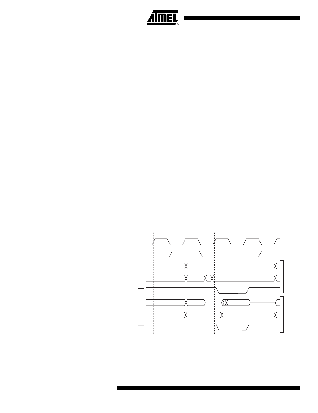
105 on page 202). The different wait states are set up in software. As an additional feature, it is possible to divi de the exte rnal memory spac e in two sector s with ind ividual wai t
state settings. This makes it possible to connect two different memory devices with different timing requirements to the same XMEM interface. For XMEM interface timing
details, please refer to Figure 89 to Fig ure 92, and Table 98 to Table 105.
Note that the XMEM interface is asynchronous and that the waveforms in the figures
below are related to the i ntern al syst em cloc k. The skew bet ween the I nternal and Exter nal clock (XTAL1) is not gu aranteed ( it var ies bet ween devices , temperat ure, and supply
voltage). Consequently, the XMEM interface is not suited for synchronous operation.
Figure 13. External Data Memory Cycles without Wait State (SRWn1 = 0 and
SRWn0 = 0)
System Clock (CLK
Note: 1. SRWn1 = SRW11 (upper sector) or SRW01 (lower sector), SRWn0 = SRW10 (upper
(1)
CPU
ALE
A15:8
DA7:0
WR
DA7:0 (XMBK = 0)
DA7:0 (XMBK = 1)
RD
T1 T2 T3
)
AddressPrev. Addr.
Address DataPrev. Data XX
DataPrev. Data Address
DataPrev. Data Address
T4
sector) or SRW00 (lower sector)
The ALE pulse in period T4 is only present if the next instruction accesses the RAM
(internal or external).
Write
Read
26
ATmega8515(L)
2512F–AVR–12/03
Page 27
ATmega8515(L)
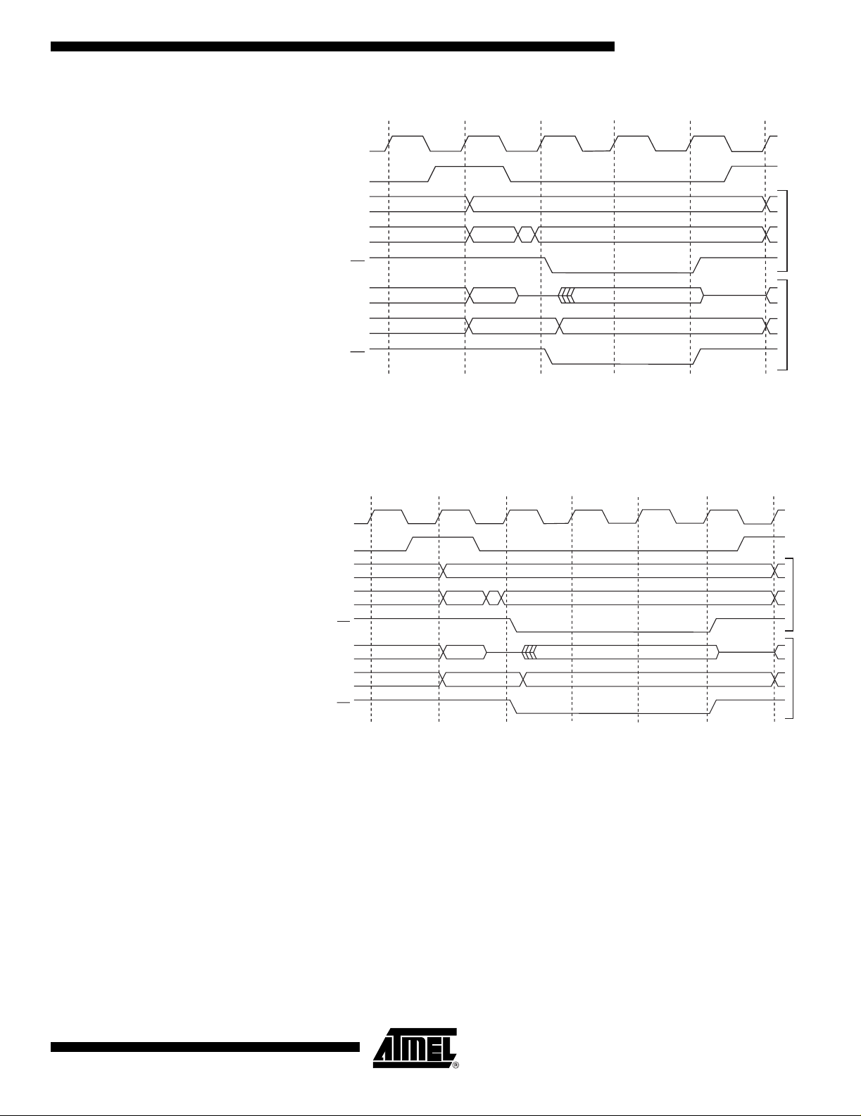
Figure 14. External Data Memory Cycles with SRWn1 = 0 and SRWn0 = 1
System Clock (CLK
DA7:0 (XMBK = 0)
DA7:0 (XMBK = 1)
CPU
ALE
A15:8
DA7:0
WR
RD
T1 T2 T3
)
AddressPrev. Addr.
Address DataPrev. Data XX
DataPrev. Data Address
DataPrev. Data Address
T4
(1)
T5
Note: 1. SRWn1 = SRW11 (upper sector) or SRW01 (lower sector), SRWn0 = SRW10 (upper
sector) or SRW00 (lower sector)
The ALE pulse in period T5 is only present if the next instruction accesses the RAM
(internal or external).
Figure 15. External Data Memory Cycles with SRWn1 = 1 and SRWn0 = 0
System Clock (CLK
CPU
T1 T2 T3
)
T4 T5
(1)
T6
Write
Read
ALE
A15:8
DA7:0
WR
DA7:0 (XMBK = 0)
DA7:0 (XMBK = 1)
Address DataPrev. Data XX
RD
AddressPrev. Addr.
DataPrev. Data Address
DataPrev. Data Address
Note: 1. SRWn1 = SRW11 (upper sector) or SRW01 (lower sector), SRWn0 = SRW10 (upper
sector) or SRW00 (lower sector)
The ALE pulse in period T6 is only present if the next instruction accesses the RAM
(internal or external).
Write
Read
2512F–AVR–12/03
27
Page 28
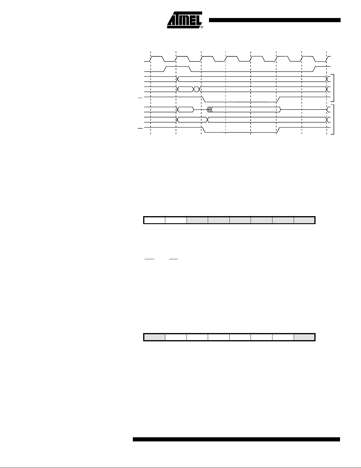
Figure 16. External Data Memory Cycles with SRWn1 = 1 and SRWn0 = 1
System Clock (CLK
CPU
)
T1 T2 T3
ALE
T4 T5 T6
(1)
T7
XMEM Register Description
MCU Control Register – MCUCR
A15:8
DA7:0
WR
DA7:0 (XMBK = 0)
DA7:0 (XMBK = 1)
Address DataPrev. Data XX
RD
AddressPrev. Addr.
DataPrev. Data Address
DataPrev. Data Address
Note: 1. SRWn1 = SRW11 (upper sector) or SRW01 (lower sector), SRWn0 = SRW10 (upper
sector) or SRW00 (lower sector)
The ALE pulse in period T7 is only present if the next instruction accesses the RAM
(internal or external).
Bit 76543210
SRE SRW10
Read/Write R/W R/W R/W R/W R/W R/W R/W R/W
Initial Value00000000
SE SM1 ISC11 ISC10 ISC01 ISC00 MCUCR
• Bit 7 – SRE: Exte r n a l S R A M /XMEM Enable
Write
Read
Extended MCU Control Register – EMCUCR
Writing SRE to one enables the External Memory Interface.The pin functions AD7:0,
A15:8, ALE, WR
, and RD are activated as the alternate pin functions. The SRE bit overrides any pin direction settings in the respective Data Direction Registers. Writing SRE
to zero, disables the Ext ernal Me mo ry Interfac e and th e n ormal pin a nd data di rection
settings are used.
• Bit 6 – SRW10: Wait State Select Bit
For a detailed description, see common description for the SRWn bits below (EMCUCR
description).
Bit 76543210
SM0 SRL2SRL1SRL0SRW01SRW00SRW11ISC2 EMCUCR
Read/Write R/W R/W R/W R/W R/W R/W R/W R/W
Initial Value00000000
• Bit 6..4 – SRL2, SRL1, SRL0: Wait State Sector Limit
It is possible to configure different wait states for different external memory addresses.
The External Memory address space can be di vided in two sectors that have sepa rate
wait state bits. The SRL2, SRL1, and SRL0 bits select the spl itting of these sectors, see
Table 2 and Figure 11. By default, the SRL2, SRL1, and SRL0 bits are set to zero and
the entire External Memory address space is treated as one sector. When the entire
28
ATmega8515(L)
2512F–AVR–12/03
Page 29

ATmega8515(L)
SRAM address space is configured as one sector, the wait states are configured by the
SRW11 and SRW10 bits.
Table 2. Sector Limits with Different Settings of SRL2..0
SRL2 SRL1 SRL0 Sector Limits
000
001
010
011
100
101
110
111
Lower sector = N/A
Upper sector = 0x0260 - 0xFFFF
Lower sector = 0x0260 - 0x1FFF
Upper sector = 0x2000 - 0xFFFF
Lower sector = 0x0260 - 0x3FFF
Upper sector = 0x4000 - 0xFFFF
Lower sector = 0x0260 - 0x5FFF
Upper sector = 0x6000 - 0xFFFF
Lower sector = 0x0260 - 0x7FFF
Upper sector = 0x8000 - 0xFFFF
Lower sector = 0x0260 - 0x9FFF
Upper sector = 0xA000 - 0xFFFF
Lower sector = 0x0260 - 0xBFFF
Upper sector = 0xC000 - 0xFFFF
Lower sector = 0x0260 - 0xDFFF
Upper sector = 0xE000 - 0xFFFF
• Bit 1 and Bit 6 MCUCR – SRW11, SRW10: Wait State Select Bits for Upper
Sector
The SRW11 and SRW1 0 bits control th e numb er of wait states for the upper se ctor of
the External Memory address space, see Table 3.
• Bit 3..2 – SRW01, SRW00: Wait State Select Bits for Lower Sector
2512F–AVR–12/03
The SRW01 and SR W00 bits cont rol the number of wait states for the lower secto r of
the External Memory address space, see Table 3.
Table 3. Wait States
SRWn1 SRWn0 Wait States
0 0 No wait states.
0 1 Wait one cycle during read/write strobe.
1 0 Wait two cycles during read/write strobe.
11
Note: 1. n = 0 or 1 (lower/upper sector).
For further details of the timing and wait states of the External Memory Interface, see
Figure 13 to Figure 16 how the setting of the SRW bits affects the timing.
(1)
Wait two cycles during read/write and wait one cycle before driving out
new address.
29
Page 30

Special Function IO Register – SFIOR
Bit 76543210
– XMBK XMM2 XMM1 XMM0 PUD – PSR10 SFIOR
Read/Write R/W R/W R/W R/W R/W R/W R/W R/W
Initial Value00000000
• Bit 6 – XMBK: External Memory Bus Keeper Enable
Writing XMBK to one enables the Bus Keeper on the AD7:0 line s. When the Bus Keeper
is enabled, AD7:0 will keep the last driven val ue on the lines even if the XMEM interface
has tri-stated the lines. Writing XMBK to zero disables the Bus Keeper. XMBK is not
qualified with SRE, so even if the XMEM interface is disabled, the Bus Keepers are still
activated as long as XMBK is one.
• Bit 5..3 – XMM2, XMM1, XMM0: External Memory High Mask
When the External Memory is enabled, all Port C pins are used for the high address
byte by default. If the full 64,928 bytes address space is not required to access the
External Memory, some, or all, Port C pins can be released for normal Port Pin function
as described in Table 4. As described in “Using all 64KB Locations of External Memory”
on page 32, it is possible to use t he XMMn bits to acc ess all 64 KB locati ons of the Exter nal Memory.
Table 4. Port C Pins Released as Normal Port Pins when the External Memory is
Enabled
XMM2 X MM1 XMM0 # Bits for External Memory Address Released Port Pins
Using all Locations of External Memory Small er than 64 KB
0 0 0 8 (Full 64,928 Bytes Space) None
0017 PC7
0106 PC7 - PC6
0115 PC7 - PC5
1004 PC7 - PC4
1013 PC7 - PC3
1102 PC7 - PC2
1 1 1 No Address High bits Full Port C
Since the external memory is mapped after the internal memory as shown in Figure 11,
the external me mory is not addre ssed when ad dressing the fir st 608 bytes of d ata
space. It m ay appe ar that t he firs t 608 byte s of the ext erna l me mory are ina ccess ible
(external memory addresses 0x0000 to 0x025F). Ho wever, whe n connecting an external memory smaller than 64 KB, for exampl e 32 KB, these lo cations are easily acces sed
simply by address ing from addres s 0x8000 to 0x8 25F. Since the External Memory
Address bit A15 is not connected to the external memory, addresses 0x8000 to 0x825F
will appear as addresses 0x0000 to 0x025F for the external memory. Addressing above
address 0x825F is not recommended, since this will address an external memory location that is already accessed by anoth er (lower) address. To the Ap plication softw are,
the external 32 KB memory will appear as one linear 32 KB address space from 0x0260
to 0x825F. This is illustrat ed in Fi gure 17.
30
ATmega8515(L)
2512F–AVR–12/03
Page 31

Figure 17. Address Map with 32 KB External Memory
Memory Configuration
ATmega8515(L)
0x0000
0x025F
0x0260
0x7FFF
0x8000
0x825F
0x8260
AVR Memory Map
Internal Memory
External
Memory
External 32K SRAM
0x0000
0x025F
0x0260
0x7FFF
2512F–AVR–12/03
(Unused)
0xFFFF
31
Page 32

Using all 64KB Locations of External Memory
Since the External Memory is mapped after the Internal Memory as shown in Figure 11,
only 64,928 bytes of External Memory is available by default (address space 0x0000 to
0x025F is res erved fo r Inte rnal Me mo ry). How ever, it is po ssible to take ad vantage of
the entire External Memory by masking the higher address bits to zero. This can be
done by using the XMMn bits and control by software the most significant bits of the
address. By setting Port C to ou tput 0x00, and releasing the most sig nificant bits for normal Port Pin operation, the Memory Interface will address 0x0000 - 0x1FFF. See code
example below.
Assembly Code Example
; OFFSET is defined to 0x2000 to ensure
; external memory access
; Configure Port C (address high byte) to
; output 0x00 when the pins are released
; for normal Port Pin operation
ldi r16, 0xFF
out DDRC, r16
ldi r16, 0x00
out PORTC, r16
; release PC7:5
ldi r16, (1<<XMM1)|(1<<XMM0)
out SFIOR, r16
; write 0xAA to address 0x0001 of external
; memory
ldi r16, 0xaa
sts 0x0001+OFFSET, r16
; re-enable PC7:5 for external memory
ldi r16, (0<<XMM1)|(0<<XMM0)
out SFIOR, r16
; store 0x55 to address (OFFSET + 1) of
; external memory
ldi r16, 0x55
sts 0x0001+OFFSET, r16
C Code Example
(1)
(1)
32
#define OFFSET 0x2000
void XRAM_example(void)
{
unsigned char *p = (unsigned char *) (OFFSET + 1);
DDRC = 0xFF;
PORTC = 0x00;
SFIOR = (1<<XMM1) | (1<<XMM0);
*p = 0xaa;
SFIOR = 0x00;
*p = 0x55;
}
Note: 1. The example code assumes that the part specific header file is included.
Care must be exercised using this option as most of the memory is masked away.
ATmega8515(L)
2512F–AVR–12/03
Page 33

System Clock and Clock Options
ATmega8515(L)
Clock Systems and their Distribution
Figure 18 presen ts the princip al clo ck system s in the AV R and the ir distributi on. All of
the clocks need not be active at a given time. In order to redu ce power consump tion, the
clocks to modules not being used can be halted by using different sleep modes, as
described in “Power Management and Sleep Modes” on page 40. The clock systems
are detailed below.
Figure 18. Clock Distribution
General I/O
Modules
clk
I/O
AVR Clock
Control Unit
CPU Core RAM
clk
CPU
clk
FLASH
Reset Logic
Watchdog Timer
Flash and
EEPROM
CPU Clock – clk
I/O Clock – clk
I/O
CPU
External RC
Oscillator
Source clock
Clock
Multiplexer
External Clock
Crystal
Oscillator
Watchdog clock
Watchdog
Low-frequency
Crystal Oscillator
Oscillator
Calibrated RC
Oscillator
The CPU clock is routed to parts of the system concerned with operation of the AVR
core. Examples of such module s are the General Purpose Reg ister File, the Stat us Register, and the Data memory holding the Stack Pointer. Halt ing the CPU clock inhibits the
core from performing general operations and calculations.
The I/O clock is used by the majority of the I/O modules, like Timer/Counters, SPI, and
USART. The I/O clock is also used by the External Interrupt module, but note that some
external inter rupts are d etected by as ynchrono us logic, al lowing suc h interrup ts to be
detected even if the I/O clock is halted.
2512F–AVR–12/03
33
Page 34

Flash Clock – clk
FLASH
The Flash clock controls operation of the Flash interface. The Flash clock is usually
active simultaneously with th e CPU clock.
Clock Sources The device has the following clock source options, selectable by Flash Fuse bits as
shown below. The clock from the selected source is input to the A VR cl ock gene rator,
and routed to the appropriate module s.
Table 5. Device Clocking Options Select
Device Clocking Option CKSEL3..0
External Crystal/Ceramic Resonator 1111 - 1010
External Low-frequency Crystal 1001
External RC Oscillator 1000 - 0101
Calibrated Internal RC Oscillator 0100 - 0001
External Clock 0000
Note: 1. For all fuses “1” means unprogrammed while “0” means programmed.
(1)
The various choices for each clocki ng optio n is given i n the followi ng secti ons. When the
CPU wakes u p from P ower-dow n or Po wer-sa ve, the sel ected cl ock so urce is used to
time the start-up, ens uring st able Osci llat or op erati on before i nstruc tion exe cuti on star ts.
When the CPU starts from Reset, there is as an additional delay allowing the pow er to
reach a stable level before com mencing norm al operation. The W atchdog Oscil lator is
used for timing this real-ti me part of the sta rt-up time. The number of WDT Osc illator
cycles used f or each ti me-out i s sho wn in Ta ble 6. The fr equency of th e Watchdog Osci llator is voltage dependent as shown in “ATmega8515 Typical Characteristics” on page
205.
Table 6. Number of Watchdog Oscillator Cycles
Typ Time-out (VCC = 5.0V) Typ Time-out (VCC = 3.0V) Number of Cycles
4.1 ms 4.3 ms 4K (4,096)
65 ms 69 ms 64K 65,536)
Default Clock Source The device is shipped w ith CKS EL = “0001” and SU T = “10”. T he default clock source
setting is therefore the Internal RC Oscillator with lon gest start-up time. This default setting ensures that all use rs can make t heir desired clock sou rce setting using an InSystem or Parallel Programming.
Crystal Oscillator XTAL1 and XTAL2 are input a nd output, respectively, of an inverting amplifier which can
be configured for use as an On-chip Osc illator, as shown i n F igure 19. Either a quartz
crystal or a ceramic resonator may be used. The CKOPT Fuse selects between two different Oscillator amplifier modes. When CKOPT is programmed, the Oscillator output
will oscillate will a full rail-to-rail swing on the output. This mode is suitable when operating in a very noisy e nvironme nt or when the ou tput from XTAL2 drives a second clock
buffer. This mode has a wide frequency range. When CKOPT is unprogrammed, the
Oscillator has a smaller output swing. T his reduces power consumption conside rably.
This mode has a limited frequency range and it can not be used to drive other clock
buffers.
For resonators, the maximum frequency is 8 MHz with CK OPT unpro grammed and
16 MHz with CKOPT programmed. C1 and C2 should always be equal for both crystals
and resonators. The optimal value of the capacitors depends on the cryst al or resonator
34
ATmega8515(L)
2512F–AVR–12/03
Page 35

ATmega8515(L)
in use, the amount of stray capacitance, an d the electromagn etic noise of the environment. Some initial gu ideline s for choosing capa citors for use with c rystals are g iven in
Table 7. For ceramic resonators, the capac itor values given by the manufacturer should
be used.
Figure 19. Crystal Oscillator Connections
C2
C1
XTAL2
XTAL1
GND
The Oscillator can operate in three different modes, each optimized for a specific frequency range. The operating mode is selected by the fuses CKSEL3..1 as shown in
Table 7.
Table 7. Crystal Oscillator Operating Modes
Frequency Range
CKOPT CKSEL3..1
1 101
1 110 0.9 - 3.0 12 - 22
1 111 3.0 - 8.0 12 - 22
0 101, 110, 111 1.0 ≤ 12 - 22
Note: 1. This option should not be used with crystals, only with ceramic resonators.
(1)
(MHz)
0.4 - 0.9 –
Recommend ed Ra nge f or Cap acit ors
C1 and C2 for Use with Crystals (pF)
2512F–AVR–12/03
The CKSEL0 Fuse together with the SUT1..0 Fuses select the start-up times as shown
in Table 8.
Table 8. Start-up Times for the Crystal Oscillator Clock Selection
Start-up Time
CKSEL0 SUT1..0
0 00 258 CK
0 01 258 CK
010 1K CK
011 1K CK
100 1K CK
from Power-down
(2)
(2)
(2)
(1)
(1)
Additional Delay from
Reset (VCC = 5.0V)
4.1 ms Ceramic resonator,
65 ms Ceramic resonator,
– Ceramic resonator,
4.1 ms Ceramic resonator,
65 ms Ceramic resonator,
Recommended
Usage
fast rising power
slowly rising power
BOD enabled
fast rising power
slowly rising power
35
Page 36

Table 8. Start-up Times for the Crystal Oscillator Clock Selection (Continued)
Low-frequency Crystal Oscillator
Start-up Time
CKSEL0 SUT1..0
1 01 16K CK – Crystal Oscillator,
1 10 16K CK 4.1 ms Crystal Oscillator, fast
1 11 16K CK 65 ms Crystal Oscillator,
Notes: 1. These options should only be used when not operating close to the maximum fre-
quency of the device, and only if frequency stability at start-up is not important for the
application. These options are not suitable for crystals.
2. These options are intended for use with ceramic resonators and will ensure frequency stability at start-up. They can also be used with crystals when not operating
close to the maximum frequency of the device, and if frequency stability at start-up is
not important for the application.
from Power-down
Additional Delay from
Reset (VCC = 5.0V)
Recommended
Usage
BOD enabled
rising power
slowly rising power
To use a 32.7 68 kHz watch crystal as th e clock source for the d evice, the Low-frequency Crystal Oscillator must be selected by setting the CKSEL Fuses to “1001”. The
crystal should be connected as shown in Figure 19. By programming the CKOPT Fuse,
the user can enable internal capacitors on XTAL1 and XTAL2, thereby removing the
need for external capacitors. The internal capacitors have a nominal value of 36 pF.
When this Oscilla tor is sele cted, sta rt-up times are determ ined by the SUT Fuse s as
shown in Table 9.
Table 9. Start-up Times for the Low-frequency Crystal Oscillator Clock Select ion
Start-up Time
SUT1..0
00 1K CK
01 1K CK
10 32K CK 65 ms Stable frequency at start-up
11 Reserved
Note: 1. These options should only be used if frequency stability at start-up is not important
from Power-down
(1)
(1)
for the application.
Addition al Del ay from
Reset (VCC = 5.0V ) Recommended Usage
4.1 ms Fast rising power or BOD
enabled
65 ms Slowly rising power
36
ATmega8515(L)
2512F–AVR–12/03
Page 37

ATmega8515(L)
External RC Oscillator For timing insensitive applicat ions, the external RC configuration shown in Figure 20
can be used. The frequency is roughly estimated by the equation f = 1/(3RC). C should
be at least 22 pF. B y progra mming th e CK OPT Fus e, th e us er c an e nable an inte rnal
36 pF capacito r between XTAL1 and GND, th ereby removing the need for an external
capacitor.
Figure 20. External RC Configuration
V
CC
R
NC
XTAL2
XTAL1
C
GND
The Oscillator can operate in four different modes, each optimized for a specific frequency range. The operating mode is selected by the fuses CKSEL3..0 as shown in
Table 10.
Table 10. External RC Oscillator Operating Modes
CKSEL3..0 Frequency Range (MHz)
0101 - 0.9
0110 0.9 - 3.0
0111 3.0 - 8.0
1000 8.0 - 12.0
When this Oscilla tor is sele cted, sta rt-up times are determ ined by the SUT Fuse s as
shown in Table 11.
2512F–AVR–12/03
Table 11. Start-up Times for the External RC Oscillator Clock Selection
Start-up Time
SUT1..0
00 18 CK – BOD enabled
01 18 CK 4.1 ms Fast rising power
10 18 CK 65 ms Slowly rising power
11 6 CK
Note: 1. This option should not be used when operating close to the maximum frequency of
from Power-down
(1)
the device.
Additional Delay from
Reset (VCC = 5.0V) Recommended Usage
4.1 ms Fast rising power or BOD
enabled
37
Page 38

Calibrated Internal RC Oscillator
The calibrated internal RC Oscillator provides a fixed 1.0, 2.0, 4.0, or 8.0 MHz clock. All
frequencies are nominal values at 5V and 25°C. This clock may be selected as the system clock by p rogram min g the CKS EL Fuse s as shown in Tabl e 12 . If selec ted, it wi ll
operate with no external components. The CKOPT Fuse should always be unprogrammed when using this clo ck optio n. Durin g reset, hardwa re loads t he cali brati on byte
into the OSCCAL Register and ther eby automat ically cal ibra tes the RC Osci llat or. At 5V,
25°C, and 1.0 MHz Oscillator frequency selected, this calibration gives a frequency
within ± 3% of the nominal frequency. Using run-time calibration methods as described
in application notes available at www.atmel.com/avr it is possible to achieve ± 1% accuracy at any given V
and Temperature. When this Oscillator is used as the chip clock,
CC
the Watchdog Oscillator will still be used for the Watchdog T imer and for the Reset
Time-out. For more information on t he pre-programmed calibration value, see the se ction “Calibration Byte” on page 179.
Table 12. Internal Calibrated RC Oscillator Operating Modes
CKSEL3..0 Nominal Frequency (MHz)
(1)
0001
0010 2.0
0011 4.0
0100 8.0
Note: 1. The device is shipped with this option selected.
1.0
When this Oscilla tor is sele cted, sta rt-up times are determ ined by the SUT Fuse s as
shown in Table 13. XTAL1 and XTAL2 should be left unconnected (NC).
Oscillator Calibrat ion Register – OSCCAL
Table 13. Start-up Times for the Internal Cali brated RC Oscillator Clock Selection
Start-up Time from
SUT1..0
00 6 CK – BOD enabled
01 6 CK 4.1 ms Fast rising powe r
(1)
10
11 Reserved
Note: 1. The device is shipped with this option selected.
Bit 76543210
Read/Write R/W R/W R/W R/W R/W R/W R/W R/W
Initial Value Device Specific C a libration Value
Power-down
6 CK 65 ms Slowly rising power
CAL7 CAL 6 CAL5 CAL4 CAL3 CAL2 CAL 1 CAL0 OSCCAL
Additional Delay from
Reset (VCC = 5.0V) Recommended Usage
• Bits 7..0 – CAL7..0: Oscillator Calibration Value
Writing the calibration byte to this address will trim the internal Oscillator to remove process variations from the Oscillator frequency. During Reset, the 1 MHz calibrated value
which is located in the signature row High Byte (address 0x00) is automatically loaded
into the OSCCAL Register. If th e inter nal RC is us ed at o ther frequen cie s, the cali bra tion
values must be loaded manually. This can be done by first reading the signature row by
a programmer, and then store the calibration values in the Flash or EEPROM. Then the
value can be read by software an d lo aded into the OSCCAL Regi ste r. When OSCCAL is
zero, the lowest available frequency is chosen. Writing non-zero va lues to this register
38
ATmega8515(L)
2512F–AVR–12/03
Page 39

ATmega8515(L)
will increase the frequency of the inter nal Oscill ator. Writi ng $FF to the regis ter gives the
highest available frequency. The calibrated Oscillator is used to time EEPROM and
Flash access. If EEPROM or Flash is written, do not calibrate to more than 10% above
the nominal fre quency. Otherw ise, the EEP ROM or F lash write m ay fai l. No te that the
Oscillator is intend ed fo r cali bration t o 1. 0, 2.0, 4.0, or 8. 0 MHz. Tuning to other values is
not guaranteed, as indicated i n Table 14.
Table 14. Internal RC Oscillator Frequency Range.
Min Frequency in Percentage of
OSCCAL Value
$00 50% 100%
$7F 75% 150%
$FF 100% 200%
Nominal Frequency
Max Frequency in Percentage of
Nominal Frequency
External Clock To drive the device from an external clock source, XTAL1 should be driven as shown in
Figure 21. To run the de vice on an exte rnal clock, the CK SEL Fuses must be programmed to “0000”. By programming the CKOPT Fuse, the user can enable an internal
36 pF capacitor between XTAL1 and GND.
Figure 21. External Clock Drive Configuration
EXTERNAL
CLOCK
SIGNAL
2512F–AVR–12/03
When this clock source is selected, start-up times are determined by the SUT Fuses as
shown in Table 15.
Table 15. Start-up Times for the External Clock Selection
Start-up Time from
SUT1..0
00 6 CK – BOD enabled
01 6 CK 4.1 ms Fast rising power
10 6 CK 65 ms Slowly rising power
11 Reserved
Power-down
Additional Delay from
Reset (VCC = 5.0V) Recommended Usage
When applying an external clock, it is required to avoid sudden changes in the applied
clock frequency to ensure stable operation of the MCU. A variation in frequency of more
than 2% from one clock cycle to the next can lead to unpredictable behavior. It is
required to ensu re that th e MCU is kept in Reset during such changes in the clock
frequency.
39
Page 40

Power Management and Sleep Mo des
Sleep modes enable the application to shut down unused modules in the MCU, thereby
saving power. The AVR provides various sleep modes allowing the user to tailor the
power consumption to the application’s requirements.
To enter any of the three sleep modes, the SE bit in MCUC R must be written to logic
one and a SLEEP instruction must be executed. The SM2 bit in MCUCSR, the SM1 bit
in MCUCR, and the SM0 bit in the EMCUCR Register select which sleep mode (Idle,
Power-down, or Standby) will be activated by the SLEEP instruction. See Table 16 for a
summary. If an ena bled int errup t occurs while the MCU is in a sl eep mo de, the M CU
wakes up. The MCU is then halted for four cycles in addition to the start-up time, it executes the interrupt routi ne, and res umes executi on from the i nstructi on foll owing SLEEP.
The contents of the R egister F ile and SRA M are u naltered w hen the device wa kes up
from sleep. If a Reset occurs during sl eep mo de, t he MCU wakes up and execu tes from
the Reset Vector.
Figure 18 on page 33 presents the different clock systems in the ATmega8515, and
their distribution. The figure is helpful in selecting an appropriate sleep mode.
MCU Control Register – MCUCR
MCU Control and Status Register – MCUCSR
Bit 76543210
SRE SRW10 SE SM1 ISC11 ISC10 ISC01 ISC00 MCUCR
Read/Write R/W R/W R/W R/W R/W R/W R/W R/W
Initial Value00000000
• Bit 5 – SE: Sleep Enable
The SE bit must be written to lo gic one t o make the MCU enter the sle ep mode when the
SLEEP instruction is executed. To avoi d the MCU entering the sleep mode unl ess it is
the programmers purpose, it is recommended to write the Sleep Enable (SE) bit to one
just before the execution of the SLEEP instruction and to clear it immediately after waking up.
• Bit 4 – SM1: Sleep Mode Select Bit 1
The Sleep Mode Select bits select between the three available sleep modes a s shown
in Table 16.
Bit 76543210
– –SM2– W DRF BORF EXTRF PORF MCUCSR
Read/Write R/W R/W R/W R/W R/W R/W R/W R/W
Initial Value00000000
• Bit 5 – SM2: Sleep Mode Select Bit 2
The Sleep Mode Select bits select between the three available sleep modes a s shown
in Table 16.
40
ATmega8515(L)
2512F–AVR–12/03
Page 41

ATmega8515(L)
Extended MCU Control Register – EMCUCR
Bit 76543210
SM0
Read/Write R/W R/W R/W R/W R/W R/W R/W R/W
Initial Value00000000
SRL2 SRL1 SRL0 SRW01 SRW 00 SRW11 ISC2 EMCUCR
• Bits 7 – SM0: Sleep Mode Select Bit 0
The Sleep Mode Select bits select between the three available sleep modes a s shown
in Table 16.
Table 16. Sleep Mode Select
SM2 SM1 SM0 Sleep Mode
000Idle
001Reserved
0 1 0 Power-down
011Reserved
100Reserved
101Reserved
1 1 0 Standby
111Reserved
Note: 1. Standby mode is only available with external crystals or resonators.
(1)
Idle Mode When the SM2..0 bit s are written to 000, the SLEE P instructi on makes the MCU enter
Idle mode, stopping the CPU but allowing SPI, USART, Analog Comparator,
Timer/Counters, Watchdog, and the Interrupt System to continue operating. This sleep
mode basically halts clk
CPU
and clk
, while allowing the other clocks to run.
FLASH
Idle mode enables the MCU to wake up from external triggered interrupts as well as
internal ones like the Timer Overflow and USART Transmit Complete interrupts. If
wake-up from the Analog Comparator interrupt is not required, the Analog Comparator
can be powered down by setting the ACD bit in the Analog Compar ator Control and Status Register – ACSR. This will reduce power consumption in Idle mode.
Power-down Mode When the SM 2..0 bits are written t o 010, t he SLEE P instruction m akes t he MCU ent er
Power-down mode. I n this mode , the ex ternal O scillator is sto pped, whi le the External
Interrupts and the Watchdog continue operating (if enabled). Only an External Reset, a
Watchdog Reset, a Brown-out Reset, an External level interrupt on INT0 or INT1, or an
External interrupt on INT2 can wake up the MCU. This sleep mode basically halts all
generated clocks, allowing operation of asynchronous modules only.
Note that if a level triggered interrupt is used for wake-up f rom Power-down mode, the
changed level must be held for some time to wake up the MCU. Refer to “External Inter rupts” on page 76 for details.
When waking up from Power-down mode, there is a delay from the wake -up con dition
occurs until the wake-up becomes effective. This allows the clock to r estart and become
stable after having been stopp ed. The wake-u p p eriod is defined b y th e same CKS EL
Fuses that define the Reset Time-out period, as described in “Clock Sources” on page
34.
2512F–AVR–12/03
41
Page 42

Standby Mode When the SM2..0 bits are written to 110, and an external crystal/resonator clock option
is selected, the SLEEP instruction m akes the MCU enter Stand by mode. Thi s mode is
identical to Power-down with the exception that the Oscillator is kept running. From
Standby mode, the device wakes up in six clock cycles.
Table 17. Active Clock Domains and Wake-up Sources in the Different Sleep Modes
Active Clock domains Oscillators Wake-up Sources
Main Clock
Sleep Mode clk
Idle
Power-down X
Standby
Notes: 1. External Crystal or resonator selected as clock source
(1)
2. Only INT2 or level interrupt INT1 and INT0
CPU
clk
FLASH
clk
Source Enabled
IO
XXXXX
XX
INT2
INT1
INT0
(2)
(2)
SPM/
EEPROM
Ready Other I/O
Minimizing Power Consumption
There are several issues to consider when trying to minimize the power consumption in
an AVR controlled system. In general, sleep modes should be used as much as possible, and the slee p mode shoul d be se lected s o that as few a s p ossible of the devi ce’s
functions are op erating. A ll function s no t needed shoul d be d isabled. In part icular, the
following modules may need special consideration when trying to achieve the lowest
possible power consumption.
Analog Comparator When entering Idle mode, the Analog Compa rator should be disabled if not needed. In
the other sleep modes, the Analog Comparator is automatically disabled. However, if
the Analog Comparator is set up to use the Internal Voltage Reference as input, the
Analog Comparator should be disabled in all sleep modes. Otherwise, the Internal Voltage Reference will be ena bled, independent of sleep mode. Refer to “Analog
Comparator” on page 162 for details on how to configure the Analog Comparator.
Brown-out Detector If the Brown-out Detector is not needed in the application, this module should be turned
off. If the Brown-out Detector is enable d by the BODEN Fuse, it will be ena bled in all
sleep modes, and hence, always consum e power. In the de eper sleep mod es, this will
contribute significantly to the total current consumption. Refer to “Brown-out Detection”
on page 47 for details on how to configure the Brown-out Detector.
Interna l Voltage Refe re n c e The Internal Voltage Referen ce will be enabled when needed by the Brown-o ut Detecto r
or the Analog Co mp arator. If these modules are disab led as d escribed in the s ections
above, the internal voltage reference will be disabled and it will not b e consuming
power. When turned on again, the user must al low the reference to start up before the
output is used. If the reference is kept on in sleep mode, the output can be used immediately. Refer t o “Internal Voltage Reference” on page 49 for details on the star t-up time.
Watchdog Timer If the Watc hdog Timer is not needed in the applic ati on, this module should be turned off.
If the Watchdog Timer is enab led, it will be ena bled in all sleep modes, and hence,
always consume power. In the deeper sleep mo des, this will contribute significant ly to
the total current co nsumption . Refer to page 52 for details on h ow to conf igure the
Watchdog Timer.
42
ATmega8515(L)
2512F–AVR–12/03
Page 43

ATmega8515(L)
Port Pins When entering a sleep mode, all port pins should be configured to use minimum power.
The most important thing is to ensure that no pins drive resistive loads. In sleep modes
where the I/O clock (clk
This ensures that no power is co nsumed b y the input logic w hen not needed . In som e
cases, the input logic is needed for detecting wake-up conditions, and it will then be
enabled. Refer to the section “Digital Input Enable and Sleep Modes” on page 62 for
details on which pins are enabled. If the input buffer is enabl ed and the input signal is
left floating or have an analog signal level close to V
sive power.
) is stopped, the input buffers of the device will be disabled.
I/O
/2, the input buffer will use exces-
CC
2512F–AVR–12/03
43
Page 44

System Control and Reset
Resetting the AVR During Reset, all I/O Registers are set to their initial values, and t he program starts exe-
cution from the Reset Vector. The instruction placed at the Reset Vector must be a
RJMP instruction to the reset handli ng routine. If the program never enable s an interrupt
source, the Interrupt Vectors are not used, and regular program code can be placed at
these locations. This is also the case if the R eset Vector is in the A pplication section
while the Interrupt Vectors are in the Boot sect ion or vice versa. Th e circuit diagram in
Figure 22 shows the reset logic. Table 18 defines the electrical parameters of the reset
circuitry.
The I/O ports of the AVR are immediately reset to their initial state when a reset source
goes active. This does not require any clock source to be running.
After all reset sources have gone inactive, a delay counter is invoked, stretching the
internal reset. This allows the power to reach a stable level before normal operation
starts. The time-out period of the delay counter is defined by the user through the
CKSEL Fuses. The different selections for the delay period are presented in “Clock
Sources” on page 34.
Reset Sources The ATmega8515 has four sources of reset:
• Power-on Reset. The MCU is reset when the supply volt age is below the Power-on
Reset threshold (V
• External Reset. The MCU is reset when a lo w level is present on the RESET
longer than the minimum pulse length.
• Watchdog Reset. The MCU is reset when the Watchdog Timer period expires and
the Watchdog is enabled.
• Brown-out Reset. The MCU is reset when the supply voltage V
Brown-out Reset threshol d (V
POT
).
pin for
is below the
) and the Brown-out Detector is enabled.
BOT
CC
44
ATmega8515(L)
2512F–AVR–12/03
Page 45

Figure 22. Reset Logic
Power-on
Reset Circuit
ATmega8515(L)
DATA BUS
MCU Control and Status
Register (MCUCSR)
BORF
PORF
WDRF
EXTRF
BODEN
BODLEVEL
Pull-up Resistor
Spike
Filter
Brown-out
Reset Circuit
Reset Circuit
Watchdog
Timer
Watchdog
Oscillator
Clock
Generator
CKSEL[3:0]
SUT[1:0]
CK
Delay Counters
TIMEOUT
Table 18. Reset Characteristics
Symbol Parameter Condition Min Typ Max Units
Power-on Reset Threshold
Voltage (rising)
V
POT
Power-on Reset Threshold
(1)
Voltage (falling)
V
V
V
t
RST
t
BOD
HYST
RST
BOT
RESET Pin Threshold Voltage 0.1 0.9 V
Minimum pulse width on
Pin
RESET
Brown-out Reset Threshold
(2)
Voltage
Minimum lo w v oltag e period f or
Brown-out Detection
BODLEVEL = 1 2.5 2.7 3.2
BODLEVEL = 0 3.7 4.0 4.2
BODLEVEL = 1 2 µs
BODLEVEL = 0 2 µs
Brown-out Detector h ystere s is 130 mV
Notes: 1. The Power-on Reset will not work unless the supply voltage has been below V
(falling).
2. V
may be below nominal minimum operating voltage for some devices. For
BOT
devices where this is the case, the device is tested down to V
production test. This guarantees that a Brown-out Reset will occur before VCC drops
to a voltage where correct operation of the microcontroller is no longer guaranteed.
The test is perfor med using BO DLEVEL=1 for ATmega8515L and BODLEVEL=0 for
ATmega8515. BODLEVEL=1 is not applicable for ATmega8515.
1.4 2.3 V
1.3 2.3 V
1.5 µs
CC
= V
duri ng the
BOT
CC
V
POT
2512F–AVR–12/03
45
Page 46

Power-on Reset A Power-on Reset (POR) pulse is generated by an On-chip detection circuit. The detec-
tion level i s defined in Table 18. Th e POR is a ctivated w heneve r V
is below the
CC
detection level. The POR circuit can be used to trigger the Start-up Reset, as well as to
detect a failure in supply volt age.
A Power-on Reset (POR) circuit ensures that the device is reset from Power-on. Reaching the Power-on Reset threshold voltage invokes the delay counter, which determines
how long the device is kept in RESET after V
again, without any delay, when V
decreases below the detection level .
CC
rise. The RESET signal is activated
CC
t
TOUT
Tied to V
CC
Figure 23. MCU Start-up, RESET
V
V
CC
RESET
TIME-OUT
INTERNAL
RESET
POT
V
RST
Figure 24. MCU Start-up, RESET Extended Externally
V
V
CC
RESET
TIME-OUT
POT
V
RST
t
TOUT
46
INTERNAL
RESET
ATmega8515(L)
2512F–AVR–12/03
Page 47

ATmega8515(L)
External Reset An Externa l Reset is gene rated by a low level on the RES ET pin. Re set pulses longer
than the minimum pulse width (see T able 18) will generate a rese t, even if the clock is
not running. Shorter pulses are not guarante ed to generate a reset. When the applied
signal reaches the Reset Threshold Voltage – V
counter starts the MCU after the Time-out period t
Figure 25. External Reset During Operation
CC
– on its positive edge, the delay
RST
has expired.
TOUT
Brown-out Detection ATmega8515 has an On-chip Brown-out Detection (BOD) circuit for monitoring the V
level during operation by comparing it to a fixed trigge r level. The trigger level for the
BOD can be selected by the fuse BODLEVEL to be 2.7V (BODLEVEL unprogrammed),
or 4.0V (BODLE VEL program med). The tr igger leve l has a hyst eresis to ensu re s pike
free Brown-out Detection. The hysteresis on the detection level should be interpreted as
V
BOT+
= V
BOT
+ V
HYST
/2 and V
BOT-
= V
BOT
- V
HYST
/2.
The BOD circuit can be enabled/disabled by the fuse BODEN . When the BOD is
enabled (BODE N programmed), and V
in Figure 26), the Brown-out Reset is immediately activated. When VCC increases
(V
BOT-
above the trigger level (V
time-out period t
has expired.
TOUT
in Figure 26), the delay counter starts the MCU after the
BOT+
The BOD circuit will only detect a drop in V
for longer than t
given in Table 18.
BOD
decreases to a valu e below the trigger level
CC
if the voltage stays below the trigger level
CC
Figure 26. Brown-out Reset During Operation
V
CC
V
BOT-
V
BOT+
RESET
CC
2512F–AVR–12/03
TIME-OUT
INTERNAL
RESET
t
TOUT
47
Page 48

Watchdog Reset When the Watchdog times out, it will generate a short reset pulse of one CK cycle dura-
tion. On the falling edge of this puls e, the delay timer start s countin g the Time-out period
. Refer to page 52 for details on operation of the Watc hdog Timer .
t
TOUT
Figure 27. Watchdog Reset During Operation
CC
CK
MCU Control and Status Register – MCUCSR
The MCU Control and Status Register provides information on which reset source
caused an MCU Reset.
Bit 76543210
– – SM2 – WDRF BORF EXTRF PORF MCUCSR
Read/Write R/W R/W R R/W R/W R/W R/W R/W
Initial Valu e 0 0 0 See Bit Descri ption
• Bit 3 – WDRF: Watchdog Reset Fl ag
This bit is set if a Watchdog Reset occurs. The bi t is reset by a Pow er-on Reset, or by
writing a logic zero to the flag.
• Bit 2 – BORF: Brown-out Reset Flag
This bit is set if a Brown-out Reset occurs. The bit is reset by a Powe r-on Reset, or by
writing a logic zero to the flag.
• Bit 1 – EXTRF: External Reset Flag
This bit is set i f an E xternal R eset occ urs. T he bit is reset by a Power-on Reset, or by
writing a logic zero to the flag.
• Bit 0 – PORF: Power-on Reset Flag
This bit is set if a Power-on Reset occurs. The bit is reset only by writing a logic zero to
the flag.
To make use of the Reset Flags to identify a reset condition, the user should re ad and
then reset the MCUCSR as early as possible in the program. If the register is cleared
before another reset occurs, the source of the reset can be found by examining the
Reset Flags.
48
ATmega8515(L)
2512F–AVR–12/03
Page 49

ATmega8515(L)
Internal Voltage Reference
Voltage Reference Enable Signals and Start-up Time
ATmega8515 features an internal bandgap reference. This reference is used for Brownout Detection, and it can be used as an input to the Analog Comparator.
The voltage reference has a start-up time that may influence the way it should be used.
The start-up time is given i n Table 19. To s ave power, the r eference is n ot always tur ned
on. The reference is on during the follo wing situations:
1. When the BOD is enabled (by programming the BODEN Fuse).
2. When the bandgap reference is connected to the Analog Comparator (by setting
the ACB G bit in ACSR ).
Thus, when th e BO D is not en abled , afte r setti ng the ACB G bi t, the user m ust al ways
allow the reference to star t up befor e the output from the Analog Compar ator i s used. To
reduce power consumption in Power-down mode, the user can avoid the two conditions
above to ensure that the reference is turned off before entering Power-down mode.
Table 19. Internal Voltage Reference Characteristics
Symbol Parameter Min Typ Max Units
V
BG
t
BG
I
BG
Bandgap reference voltage 1.15 1.23 1.35 V
Bandgap reference start-up time 40 70 µs
Bandgap reference current consumption 10 µA
Wat c hdog Timer The Watchdog Timer is clocked from a separate On-chip Oscillator which runs at
1 MHz. T his is the typical fre quen cy at V
values at other VCC levels. By controlling the Watchdog Timer prescaler, the Watchdog
Reset interval can be adjusted as shown in Table 21 on page 51. Th e WDR – Watchdog
Reset – instruction resets the Watchdog Timer. The Watchdog Timer is also reset when
it is disabled and when a Chip Reset occurs. Eight different clock cycle periods can be
selected to determine the reset period. If the reset period expires without another
Watchdog Reset, the ATmega851 5 resets and executes f rom t he Reset Vector. For timing details on the Watchdog Reset, ref er to page 48.
= 5V. See characterization data for typical
CC
2512F–AVR–12/03
To prevent unintentional disabling of the Watchdog or unintentional change of time-out
period, three different safety levels are selected by the Fuses S8515C and WDTON as
shown in Table 20. Safety level 0 corresponds to the setting in AT90S4414/8515. There
is no restriction on enabling the WDT in any of the safety levels. Refer to “Timed
Sequences for Changin g the Con figuration of the W atchdog T imer” on page 52 for
details.
49
Page 50

Table 20. WDT Configuration as a Function of the Fuse Settings of S8515C and
WDTON.
WDT
Safety
S8515C WDTON
Unprogrammed Unprogrammed 1 Disabled Timed sequence Timed
Unprogrammed Programmed 2 Enabled Always enabled Timed
Programmed Unprogrammed 0 Disabled Timed sequence No restriction
Programmed Programmed 2 Enabled Always enabled Timed
Level
Initial
State
How to Disable
the WDT
How to
Change Timeout
sequence
sequence
sequence
Figure 28. Watchdog Timer
WATCHDOG
OSCILLATOR
Watchdog Timer Control Register – WDTCR
Bit 76543210
– – – WDCE WDE WDP2 WDP1 WDP0 WDTCR
Read/Write R R R R/W R/W R/W R/W R/W
Initial Value00000000
• Bits 7..5 – Res: Reserved Bits
These bits are reserved bit s in t he ATmega8515 and will always read as zero.
• Bit 4 – WDCE: Watchdog Change Enable
This bit must be set when the WDE bit is written to logic zero. Otherwise, the Watchdog
will not be disabled. Once written to one, hardware will clear this bit after four clock
cycles. Refer to the description of the WDE bit for a Watchdog disable procedure. In
Safety Levels 1 and 2, this b it must also be set when changi ng the prescaler bi ts. See
“Timed Sequences for Changing the Configuration of the Watchdog Timer” on page 52.
• Bit 3 – WDE: Watchdog Enabl e
When the WDE is written to l ogic one, the Watchdo g Timer i s enabled, and if the WDE is
written to logic zero, t he Watchdog Timer function is disabl ed. WDE can only be cleared
if the WDCE bit has logic level one. To disable an enabled Watchdog Timer, the following procedure must be followed:
50
ATmega8515(L)
2512F–AVR–12/03
Page 51

ATmega8515(L)
1. In the same operation, write a logic one to WDCE and WDE. A logic one must be
written to WDE even though it is set to one before the disable operation starts.
2. Within the next four clock cycles, write a logic 0 to WDE. This disables the
Watchdog.
In safety level 2, it is not possible t o disable the Watchdog Timer, even w ith the algorithm describe d abov e. See “Time d Seque nces for Cha nging the Configu ration of the
Watchdog Timer” on page 52.
• Bits 2..0 – WDP2, WDP1, WDP0: Watchdog Timer Prescaler 2, 1, and 0
The WDP2, WDP1, and WDP0 bits determine the Watchdog Timer prescaling when the
Watchdog Timer is enabled. The different prescaling values and their corresponding
Timeout Periods are shown in Table 21.
Table 21. Watchdog Ti mer Prescale Select
Number of WDT
WDP2 WDP1 WDP0
0 0 0 16K (16,384) 17.1 ms 16.3 ms
0 0 1 32K (32,768) 34.3 ms 32.5 ms
0 1 0 64K (65,536) 68.5 ms 65 ms
0 1 1 128K (131,072) 0.14 s 0.13 s
1 0 0 256K (262,144) 0.27 s 0.26 s
1 0 1 512K (524,288) 0.55 s 0.52 s
1 1 0 1,024K (1,048,576) 1.1 s 1.0 s
1 1 1 2,048K (2,097,152) 2.2 s 2.1 s
Oscillator Cycles
Typical Time-out
at VCC = 3.0V
Typical Time-out
at VCC = 5.0V
The following code example shows one assembly and one C function for turning off the
WDT. The example assumes that interrupts are controlled (e.g., by disabling interrupts
globally) so that no interrupt s wil l occur during execution of these functions.
Assembly Code Example
WDT_off:
; Write logical one to WDCE and WDE
ldi r16, (1<<WDCE)|(1<<WDE)
out WDTCR, r16
; Turn off WDT
ldi r16, (0<<WDE)
out WDTCR, r16
ret
2512F–AVR–12/03
C Code Example
void WDT_off(void)
{
/* Write logical one to WDCE and WDE */
WDTCR = (1<<WDCE) | (1<<WDE);
/* Turn off WDT */
WDTCR = 0x00;
}
51
Page 52

Timed Sequences for
Changing the
The sequence for changing c onfiguration differs slightly between the thre e safety levels.
Separate procedures are described for each level.
Configuration of the
Wat c hdog Timer
Safety Level 0 This mode is co mpatible with the Watc hdog ope ration found in A T90S4414 /8515. The
Watchdog Timer is initial ly dis abled, bu t can be enabl ed by wri ting t he WDE bit to 1 with out any restriction. The time-out period can be changed at any time without restriction.
To disable an enabled Watchdog Timer, the procedure described on page 50 (WDE bit
description) must be followed.
Safety Level 1 In this mode, the Watchdog Timer is initially disabled, but can be enabled by writing the
WDE bit to 1 without any restriction. A timed sequence is needed when changing the
Watchdog Time-out period or disablin g an enabled W atchdog Time r. To disable an
enabled Watchdog Timer, and/or changing the Watchdog Time-ou t, the f ollowing procedure must be followed:
1. In the same operation, write a logic one to WDCE and WDE. A logic one must be
written to WDE regardless of the previous value of the WDE bit.
2. Within the next f our clo c k cycle s , in the same oper at ion, write t he WDE and WDP
bits as desired, but with the WDCE bit cleared.
Safety Level 2 In this mode, the Watchdog Timer is always enabled, and the WDE bit will always read
as one. A timed sequence is needed when changing the Watchdog Time-out period. To
change the Watchdog Time-out, the followi ng procedure must be followed:
1. In the same operation, write a logical one to WDCE and WDE. Even though the
WDE always is set, the WDE must be written to one to start the timed sequence .
2. Within the next four clock cycles, in the same operation, write the WDP bits as
desired, but with the WDCE bit cleared. The value written to the WDE bit is
irrelevant.
52
ATmega8515(L)
2512F–AVR–12/03
Page 53

ATmega8515(L)
Interrupts This section describes the specifics of the interrupt handling as performe d in
ATmega8515. For a general explanat ion of the AVR interrupt ha ndling, refer to “Res et
and Interrupt Handling” on page 12.
Interrupt Vector s in ATmega8515
Table 22. Reset and Interrupt Vectors
Program
Vector No.
1 $000
2 $001 INT0 External Interrupt Request 0
3 $002 INT1 External Interrupt Request 1
4 $003 TIMER1 CAPT Timer/Counter1 Capture Event
5 $004 TIMER1 COMPA Timer/Counter1 Compare Match A
6 $005 TIMER1 COMPB Timer/Counter1 Compare Match B
7 $006 TIMER1 OVF Timer/Counter1 Overflow
8 $007 TIMER0 OVF Timer/Counter0 Overflow
9 $008 SPI, STC Serial Transfer Complete
10 $009 USART, RXC USART, Rx Complete
11 $00A USART, UDRE USART Data Register Empty
12 $00B USART, TXC USART, Tx Complete
13 $00C ANA_COMP Analog Comparator
14 $00D INT2 External Interrupt Request 2
15 $00E TIMER0 COMP Timer/Counter0 Compare Match
16 $00F EE_RD Y EEPROM Ready
Address
(2)
Source Interrupt D efinition
(1)
RESET External Pin, Power-on Reset, Brown-out
Reset and Watchdog Reset
2512F–AVR–12/03
17 $010 SPM _RDY Store Progra m memo ry Ready
Notes: 1. When the BOOTRST Fuse is programmed, the device will jump to the Boot Loader
address at reset, see “Boot Loader Support – Read-While-Write Self-Programming”
on page 164.
2. When the IVSEL bit in GICR is set, Interrupt Vectors will be moved to the start of the
Boot Flash section. The address of each Interrupt Vector will then be the address in
this table added to the start address of the Boot Flash section.
Table 23 shows Reset and Interrupt Vectors placement for the various combinations of
BOOTRST and IVSEL settings. If the program never enables an interrupt source, the
Interrupt Vectors are not used, and regular program code can be placed at these locations. This is also the case if the Reset Vector is in the Application section while the
Interrupt Vectors are in t he Boot section or vice versa.
53
Page 54

Table 23. Reset and Interrupt Vectors Placement
BOOTRST IVSEL Reset Address Interrupt Vectors Start Address
1 0 $0000 $0001
1 1 $0000 Boot Reset Address + $0001
0 0 Boot Reset Address $0001
0 1 Boot Reset Address Boot Reset Address + $0001
Note: 1. The Boot Reset Address is shown in Table 78 on page 175. For the BOOTRST Fuse
“1” means unprogrammed while “0” means programmed.
(1)
The most ty pical and gene ral program se tup for the Re set and Interru pt Vector
Addresses in ATmega8515 is:
Address Labels Code Comments
$000 rjmp RESET ; Reset Handler
$001 rjmp EXT_INT0 ; IRQ0 Handler
$002 rjmp EXT_INT1 ; IRQ1 Handler
$003 rjmp TIM1_CAPT ; Timer1 Capture Handler
$004 rjmp TIM1_COMPA ; Timer1 Compare A Handler
$005 rjmp TIM1_COMPB ; Timer1 Compare B Handler
$006 rjmp TIM1_OVF ; Timer1 Overflow Handler
$007 rjmp TIM0_OVF ; Timer0 Overflow Handler
$008 rjmp SPI_STC ; SPI Transfer Complete Handler
$009 rjmp USART_RXC ; USART RX Complete Handler
$00a rjmp USART_UDRE ; UDR0 Empty Handler
$00b rjmp USART_TXC ; USART TX Complete Handler
$00c rjmp ANA_COMP ; Analog Comparator Handler
$00d rjmp EXT_INT2 ; IRQ2 Handler
$00e rjmp TIM0_COMP ; Timer0 Compare Handler
$00f rjmp EE_RDY ; EEPROM Ready Handler
$010 rjmp SPM_RDY ; Store Program memory Ready
Handler
54
$011 RESET: ldi r16,high(RAMEND); Main program start
$012 out SPH,r16 ; Set Stack Pointer to top of RAM
$013 ldi r16,low(RAMEND)
$014 out SPL,r16
$015 sei ; Enable interrupts
$016 <instr> xxx
... ... ...
ATmega8515(L)
2512F–AVR–12/03
Page 55

ATmega8515(L)
When the BOOTRST Fuse is unprogrammed, the Boot section size set to 2K bytes and
the IVSEL bit in the GICR Register is set bef ore any interrupts are enable d, the most
typical and general prog ram setup for the Reset and Interrupt Vector Addre sses is:
Address Labels Code Comments
$000 RESET: ldi r16,high(RAMEND); Main program start
$001 out SPH,r16 ; Set Stack Pointer to top of RAM
$002 ldi r16,low(RAMEND)
$003 out SPL,r16
$004 sei ; Enable interrupts
$005 <instr> xxx
;
.org $C02
$C02 rjmp EXT_INT0 ; IRQ0 Handler
$C04 rjmp EXT_INT1 ; IRQ1 Handler
... .... .. ;
$C2A rjmp SPM_RDY ; Store Program memory Ready
Handler
When the BOOTRST Fuse is programmed and t he Boot sec tion si ze set t o 2K bytes , the
most typical and general progra m setup for the Reset and Int errupt Vector Address es is:
Address Labels Code Comments
.org $002
$001 rjmp EXT_INT0 ; IRQ0 Handler
$002 rjmp EXT_INT1 ; IRQ1 Handler
... .... .. ;
$010 rjmp SPM_RDY ; Store Program memory Ready
Handler
;
.org $C00
$C00 RESET: ldi r16,high(RAMEND); Main program start
$C01 out SPH,r16 ; Set Stack Pointer to top of RAM
$C02 ldi r16,low(RAMEND)
$C03 out SPL,r16
$C04 sei ; Enable interrupts
$C05 <instr> xxx
2512F–AVR–12/03
When the BOOTRST Fuse is programmed, the Boot sec tion size set to 2K bytes and the
IVSEL bit in the GICR Register is set bef ore any interrupts are enabled, the most typi cal
and general program setup for the Reset and Interrupt Vector Addresses is:
Address Labels Code Comments
.org $C00
$C00 rjmp RESET ; Reset handler
$C01 rjmp EXT_INT0 ; IRQ0 Handler
$C02 rjmp EXT_INT1 ; IRQ1 Handler
... .... .. ;
$C10 rjmp SPM_RDY ; Store Program memory Ready
Handler
;
$C11 RESET: ldi r16,high(RAMEND); Main program start
55
Page 56

$C12 out SPH,r16 ; Set Stack Pointer to top of RAM
$C13 ldi r16,low(RAMEND)
$C14 out SPL,r16
$C15 sei ; Enable interrupts
$C16 <instr> xxx
Moving Interrupts between Application and Boot Space
General Interrupt Control Register – GICR
The Genera l Interru pt Contr ol Reg ister co ntrols t he place ment of th e Inte rrupt Vec tor
table.
Bit 76543210
INT1 INT0 INT2 – – – IVSEL IVCE G ICR
Read/Write R/W R/W R/W R R R R/W R/W
Initial Value00000000
• Bit 1 – IVSEL: Interrupt Vector Select
When the IVSEL bit is cleared (zero), the Interrupt Vectors are placed at the start of the
Flash memory. When this bit is set (one), the Interrupt Vectors are moved to the beginning of the Boot Loader section of the Flash. The actual address of the start of the Boot
Flash section is determi ned by the B OOTSZ Fuse s. Re fer to the section “Bo ot Loa der
Support – Read-While-Write Self-Programming” on page 164 for details. To avoid unintentional changes of Interrupt Vector tables, a special write procedure must be followed
to change the IVSEL bit:
1. Write the Interrupt Vector Change Enable (IVCE) bit to one.
2. Within four cycles, write the desir ed value to IVSEL while writing a zero to IVCE.
Interrupts will automatically be disabled while this sequence is executed. Interrupts are
disabled in the cycle IVCE is set, and they remain disabled until after the instruction following the write to IVSEL. If IVSEL is not written, interrupts remain disabled for four
cycles. The I-bit in the Status Register is unaffected by the automatic disabling.
Note: If Interrupt Vectors are placed in the Boot Loa der se ction an d B oot Lo c k bi t BLB 02 is pro -
grammed, interrupts are disabled while executing from the Application section. If
Interrupt Vectors are placed in the Application section and Boot Lock bit BLB12 is programed, interrupts are disabled while executing from the Boot Loader section. Refer to
the section “Boot Loader Support – Read-While-Write Self-Programming” on page 164
for details on Boot Lock bits.
56
ATmega8515(L)
2512F–AVR–12/03
Page 57

ATmega8515(L)
• Bit 0 – IVCE: Interrupt Vector Change Enable
The IVCE bit must be writte n to logic one to enab le change of the IV SEL bit. IVCE is
cleared by hardware four cycles after it is written or when IVSEL is written. Setting the
IVCE bit will disable interrupts, as explained in the IVSEL description above. See Code
Example below.
Assembly Code Example
Move_interrupts:
; Enable change of interrupt vectors
ldi r16, (1<<IVCE)
out GICR, r16
; Move interrupts to boot flash section
ldi r16, (1<<IVSEL)
out GICR, r16
ret
C Code Example
void Move_interrupts(void)
{
/* Enable change of interrupt vectors */
GICR = (1<<IVCE);
/* Move interrupts to boot flash section */
GICR = (1<<IVSEL);
}
2512F–AVR–12/03
57
Page 58

I/O Ports
Introduction All AVR ports have true Read-Modify-Write functionality when used as general digital
I/O ports. This means that the direction of one port pin can be changed without unintentionally chang ing the direc tion of any ot her pin with the SBI and CBI instruc tions. The
same applies when changing drive value (if configured as output) or enabling/disabling
of pull-up resi stors (if configured as input). Each output buffer has symmetrical drive
characteristics with both high si nk and source capability. The pin driver is strong enough
to drive LED displays directly. All port pins have individually selectable pull-up resistors
with a supply-voltage invariant resistance. All I/O pins have protection diodes to both
and Ground as indicated in Figure 29. Refer to “Electrical Characteristics” on page
V
CC
195 for a complete list of parameters.
Figure 29. I/O Pin Equivalent Schematic
R
pu
Pxn
C
pin
All registers and bit references in this section are written in general form. A lower case
“x” represents the numbering letter for the port, and a lower case “n” represents the bit
number. However, when using the register or bit defines in a program, the precise form
must be used. For example, PORTB3 for bit no. 3 in Port B, here documented generally
as PORTxn. The physical I/O Registers and bi t locations are listed in “Register Description for I/O Ports” on page 74.
Three I/O memory address locations are allocated for each port, one each for the Data
Register – PORTx, Data Direction Regist er – DDRx, and the Port Input Pin s – PINx. The
Port Input Pins I/O location is read only, while the Data Register and the Data Direction
Register are read/writ e. In addition, the Pull-up Disable – PUD bit in SFIOR disables the
pull-up function for all pins in all ports when set.
Using the I/O port as General Digital I/O is described i n “Ports as General Digital I/O” on
page 59. Most p ort pins are multiplexed w ith alternate f unctions for the peripheral features on the device. How each alt ernate function interfe res wi th the port pin is described
in “Alternate Port Func tions” on pag e 63. Refe r to the indivi dual modu le sec tions for a
full description of the alternate functions.
See Figure
"General Digital I/O" for
Logic
Details
58
Note that enabling the al ternate function of some of the port pins does not affect the use
of the other pins in the port as general di gital I/O.
ATmega8515(L)
2512F–AVR–12/03
Page 59

ATmega8515(L)
Ports as General Digital I/O
The ports are bi-directional I/O ports with o ptional internal pull-up s. Figure 30 sh ows a
functional description of one I/O-port pin, here generically called Pxn.
Figure 30. General Digital I/O
Pxn
(1)
SLEEP
SYNCHRONIZER
DLQ
D
PINxn
Q
PUD
Q
D
DDxn
Q
CLR
RESET
Q
D
PORTxn
Q
CLR
RESET
Q
Q
WDx
RDx
WPx
RRx
RPx
DATA BUS
clk
I/O
PUD: PULLUP DISABLE
SLEEP: SLEEP CONTROL
clk
: I/O CLOCK
I/O
Note: 1. WPx, WDx, RRx, RPx, and RDx are common to all pins within the same port. clk
WDx: WRITE DDRx
RDx: READ DDRx
WPx: WRITE PORTx
RRx: READ PORTx REGISTER
RPx: READ PORTx PIN
I/O
SLEEP, and PUD are common to all ports.
Configuring the Pin Each port pin consi sts o f th ree re giste r bi ts: DD xn, P ORTx n, and P INxn. As s ho wn in
“Register Description f or I/ O Ports” on page 74, t he DDxn bit s are acc essed a t the DDRx
I/O address, the PORTxn bits at the PORTx I/O address, and the PINxn bits at the PINx
I/O address.
The DDxn bit in the DDRx Register selects the direction of this pin. If DDxn is written
logic one, Pxn is confi gured as an output pin. If DDxn is written logic zero, Pxn is configured as an input pin.
If PORTxn is written a logic one when the pin is configured as an inpu t pin, the pull-up
resistor is activated. To switch the pull-up resistor off, PORTxn has to be written a logic
zero or the pin has to be configured as an output pin. The port pins are tri-stated when a
reset condition becomes acti ve, even if no clocks are running.
If PORTxn is written a logic one when the pin is configured as an output pin, the port pin
is driven high (one). If PORTxn is written a logic zero when the pin is configured as an
output pin, the port pin is driven low (zer o).
,
2512F–AVR–12/03
When swi tching be twee n tri-sta te ({DD xn, POR Txn} = 0b 00) an d output h igh ({D Dxn,
PORTxn} = 0b11), an intermediate state with either pull-up enabled ({DDxn, PORTxn} =
0b01) or output low ({DDxn, PORTxn} = 0b10 ) must occur. Normally, the pull-up
59
Page 60

enabled state is fully acceptable, as a high-impedant environment will not notice the difference between a st rong high driver and a pull-up. If this is not the case, the PUD bit in
the SFIOR Register can be set to disable all pull-ups in all ports.
Switching between input with pull-up and output low generates the same problem. The
user must use either the tri-state ({DDxn, PORTxn} = 0b00) or the output high state
({DDxn, PORTxn} = 0b11) as an intermediate step.
Table 24 summarizes the control signa ls for the pin value.
Table 24. Port Pin Configuration s
PUD
DDxn PORTxn
0 0 X Input No Tri-state (Hi-Z)
0 1 0 Input Yes
0 1 1 Input No Tri-state (Hi-Z)
1 0 X Output No Output Low (Sink)
1 1 X Output No Output High (Source)
(in SFIOR) I/O Pull-up Comment
Pxn will source current if ext. pulled
low.
Reading the Pin Value Independent of the setting of Data Direction bit DDxn, the port pin can be read through
the PINxn Register bit. As shown in Figure 30, the PI Nxn Register bit and the preceding
latch constitute a synchronizer. This is needed to avoid metastability if the physical pin
changes value near t he edge of the internal clock, but it also introduces a delay. Figure
31 shows a t iming dia gram of th e syn chronizat ion w hen readi ng an extern ally a pplie d
pin value. The maximum and minimum propagation delays are denoted t
pd,max
and t
pd,min
respectively.
Figure 31. Synchronization when Reading an External ly Applied Pin Value
SYSTEM CLK
INSTRUCTIONS
XXX in r17, PINx
XXX
SYNC LATCH
PINxn
r17
0x00 0xFF
t
pd, max
t
pd, min
Consider the clock period starting shortly after the first falling edge of the system clock.
The latch is closed when the clock is low, and goes transparent when the clock is high,
as indicated by the shaded region of the “SYNC LATCH” signal. The signal value is
latched when the system clock goes l ow. It i s clocked into the PI Nxn Registe r at the succeeding positive clock edge . As ind icated by the two arrows t
pd,max
and t
pd,min
, a single
60
ATmega8515(L)
2512F–AVR–12/03
Page 61

ATmega8515(L)
signal transition on the pin w ill be delayed between ½ and 1½ system clock period
depending upon the time of assertion .
When reading back a software assigned pin value , a nop inst ructi on must be insert ed as
indicated in Figure 32. The out instruction sets the “SYNC LATCH” signal at the posit ive
edge of the clock. In this case, the delay t
clock period.
Figure 32. Synchronization when Reading a Software Assigned Pin Value
SYSTEM CLK
through the synchronizer is one system
pd
r16
INSTRUCTIONS
SYNC LATCH
PINxn
r17
0xFF
out PORTx, r16 nop in r17, PINx
0x00 0xFF
t
pd
2512F–AVR–12/03
61
Page 62

The following code example shows how to set port B pins 0 and 1 high, 2 and 3 low, and
define the port pins from 4 to 7 as input with pull-ups assigned to port pins 6 and 7. The
resulting pin values are read back again, but as previously discussed, a nop instruct ion
is included to be able to read back the value recently assigned to some of the pins.
Assembly Code Example
...
; Define pull-ups and set outputs high
; Define directions for port pins
ldi r16,(1<<PB7)|(1<<PB6)|(1<<PB1)|(1<<PB0)
ldi r17,(1<<DDB3)|(1<<DDB2)|(1<<DDB1)|(1<<DDB0)
out PORTB,r16
out DDRB,r17
; Insert nop for synchronization
nop
; Read port pins
in r16,PINB
...
(1)
C Code Example
unsigned char i;
...
/* Define pull-ups and set outputs high */
/* Define directions for port pins */
PORTB = (1<<PB7)|(1<<PB6)|(1<<PB1)|(1<<PB0);
DDRB = (1<<DDB3)|(1<<DDB2)|(1<<DDB1)|(1<<DDB0);
/* Insert nop for synchronization*/
_NOP();
/* Read port pins */
i = PINB;
...
Digital Input Enab le and Sleep Modes
62
ATmega8515(L)
Note: 1. For the assembly program, two temporary registers are used to minimize the time
from pull-ups are set on pins 0, 1, 6, and 7, until the direction bits are correctly set,
defining bit 2 and 3 as low and redefining bits 0 and 1 as strong high drivers.
As shown in Figure 30, the digital input signal can be clamped to ground at the input of
the Schmitt Trigger. The signal denoted S LEE P in th e figure, is se t by the MCU Sleep
Controller in Power-down mode and Standby mode to avoid high power consumption if
some input signals are left floating, or have an analog signal level close to V
CC
/2.
SLEEP is overridden for port pins enabled as External Interrupt pins. If the External
Interrupt Request is not enabled, SLEEP is active also for these pins. SLEEP is also
overridden by various other alternate functions as described in “Alternate Port Functions” on page 63.
If a logic high level (“one”) is present on an Asynchronous External Interrupt pin configured as “Interrupt on Rising Edge, Falling Edge, or Any Logic Change on Pin” while the
external interru pt is not enabled, the corres ponding External Interrupt Fl ag will be set
when resuming from the above mentioned sleep modes, as the clamping in these sleep
modes produces the requested logic change.
2512F–AVR–12/03
Page 63

ATmega8515(L)
Unconnected pins If some pins are unused, it is recommended to ensure that these pins have a defined
level. Even thoug h most o f th e di gital inpu ts ar e disa bled in the d eep s leep mod es as
described above, floating inputs should be avoided to reduce current consumption in all
other modes where the digital inputs are enabled (Reset, Active mode and I dle mode).
The simplest method to ensure a defined level of an unused pin, is to enable the internal
pull-up. In this case, the pull-up will be disabled during reset. If low power consumption
during reset is important, it is recommended to use an external pull-up or pull-down.
Connecting unused pins directly to V
cause excessive currents if the pin is accidentally configured as an output.
Alternate Port Functions Most port pins h ave alternate functions in add ition to being ge neral digital I/O s. Figure
33 shows how the port pin control signals from the simplified Figure 30 can be overridden by alternate functions . The overri ding si gnals may no t be present in all port pi ns, but
the figure serves as a generic d escription ap plicable to al l port pins in the A VR m icrocontroller family.
or GND is not recommended, since this may
CC
Figure 33. Alternate Port Functions
1
0
1
0
Pxn
1
0
1
0
(1)
PUOExn
PUOVxn
DDOExn
DDOVxn
PVOExn
PVOVxn
DIEOExn
DIEOVxn
SLEEP
SYNCHRONIZER
SET
DLQ
Q
CLR
D
PINxn
PUD
D
Q
DDxn
Q
CLR
RESET
D
Q
PORTxn
Q
CLR
RESET
Q
Q
CLR
WDx
RDx
WPx
RRx
RPx
clk
DIxn
DATA BUS
I/O
2512F–AVR–12/03
AIOxn
PUOExn: Pxn PULL-UP OVERRIDE ENABLE
PUOVxn: Pxn PULL-UP OVERRIDE VALUE
DDOExn: Pxn DATA DIRECTION OVERRIDE ENABLE
DDOVxn: Pxn DATA DIRECTION OVERRIDE VALUE
PVOExn: Pxn PORT VALUE OVERRIDE ENABLE
PVOVxn: Pxn PORT VALUE OVERRIDE VALUE
DIEOExn: Pxn DIGITAL INPUT-ENABLE OVERRIDE ENABLE
DIEOVxn: Pxn DIGITAL INPUT-ENABLE OVERRIDE VALUE
SLEEP: SLEEP CONTROL
PUD: PULLUP DISABLE
WDx: WRITE DDRx
RDx: READ DDRx
RRx: READ PORTx REGISTER
WPx: WRITE PORTx
RPx: READ PORTx PIN
: I/O CLOCK
clk
I/O
DIxn: DIGITAL INPUT PIN n ON PORTx
AIOxn: ANALOG INPUT/OUTPUT PIN n ON PORTx
Note: 1. WPx, WDx, RRx, RPx, and RDx are common to all pins within the same port. clk
SLEEP, and PUD are common to all ports. All other signals are unique for each pin.
I/O
63
,
Page 64

Table 25 su mmariz es the funct ion of the ove rriding signals. T he pin an d port indexe s
from Figure 33 are not shown in the succeeding tables. The overriding signals are generated internally in the modules having the alternate function.
Table 25. Generic Description of Over riding Signals for Alternate Functions.
Signal Name Full Name Description
PUOE Pull-up Override
Enable
PUOV Pull-up Override
Value
If this signal is set, the pull-up enable is controlled by the
PUOV signal. If this signal is cleared, the pull-up is
enabled when {DDxn, PORTxn, PUD} = 0b010.
If PUOE is set, the pull-up is enabled/disabled when
PUOV is set/cleared, regardless of the setting of the
DDxn, PORTxn, and PUD Register bits.
DDOE Data Direction
Override Enable
DDOV Data Direction
Override Value
PVOE Port Value
Override Enable
PVOV Port Value
Override Value
DIEOE Di gita l Input
Enable Ov erride
Enable
DIEOV Di gita l Input
Enable Ov erride
Value
DI Digital Input This is the Digi ta l I nput to alternate functions. In the fi gur e ,
If this signal is set, the Output Driver Enable is controlled
by the DDOV signal. If this signal is cleared, the Output
driver is enabled by the DDxn Register bit.
If DDOE is set, the Output Driver is enabled/disabled
when DDO V is set/cle ared , r egar dless of th e se tti ng of t he
DDxn Register bit.
If this signal is set and the Output Driver is enabled, the
port value is controlled by the PVOV signal. If PVOE is
cleared, and the Output Driver i s enabled, the port V alue is
controlled by the PORTxn Register bit.
If PVOE is set, the port value is set to P VOV, regardless of
the setting of the PORTxn Register bit.
If this bit is set, the Digital Input Enable is controlled by the
DIEOV signal. If this signal is cleared, the Digital Input
Enable is determined by MCU-state (Normal mode, sleep
modes).
If DIEOE is set, the Digital Input is enab led/d isab l ed when
DIEOV is set/cleared, regardless of the MCU state
(Normal mode, sleep modes).
the signal is connected to the output of the schmitt trigger
but before the synchronizer. Unless the Digital Input is
used as a clock source, the module with the alternate
function will use its own synchronizer.
64
AIO Analog
The following subsections shortly describe the alternate functions for each port, and
relate the overriding signals to the alternate function. Refer to the alternate function
description for further details.
ATmega8515(L)
Input/output
This is the Analog Input/Output to/fr om alternate functions .
The signal is connected directly to the pad, and can be
used bi-directionally.
2512F–AVR–12/03
Page 65

ATmega8515(L)
Special Function IO Register – SFIOR
Bit 7 6 5 4 3 2 1 0
– XMBK XMM2 XMM1 XMM0 PUD – PSR10 SFIOR
Read/Write R/W R/W R/W R/W R/W R/W R/W R/W
Initial Value 0 0 0 0 0 0 0 0
• Bit 2 – PUD: Pull -u p D is a bl e
When this bit is written to one, the pull-ups in the I/O ports are disabled even i f the DDxn
and PORTxn Registers are configured to enable the pull- ups ({DDxn, PORTxn} = 0b01).
See “Configuring the Pin” on page 59 for more details about this feature.
Alternate Functions of Port A Port A has an alternate function as the address low byte and data lines for the External
Memory Interface.
Table 26. Port A Pins Alternate Functions
Port Pin Alternate Function
PA7 AD7 (External memory interface address and data bit 7)
PA6 AD6 (External memory interface address and data bit 6)
PA5 AD5 (External memory interface address and data bit 5)
PA4 AD4 (External memory interface address and data bit 4)
PA3 AD3 (External memory interface address and data bit 3)
PA2 AD2 (External memory interface address and data bit 2)
PA1 AD1 (External memory interface address and data bit 1)
PA0 AD0 (External memory interface address and data bit 0)
Table 27 and Table 28 relate the alternate funct ions of Port A to the ove rriding signals
shown in Figure 33 on page 63.
Table 27. Overriding Signals for Alt ernate Functions in PA7..PA4
Signal
Name PA7/AD7 PA6/AD6 PA5/AD5 PA4/AD4
PUOE SRE SRE SRE SRE
PUOV ~(WR | ADA
PortA7
DDOE SRE SRE SRE SRE
DDOV WR | ADA WR | ADA WR | ADA WR | ADA
PVOE SRE SRE SRE SRE
PVOV A7 • ADA |
D7 OUTPUT • WR
DIEOE0 000
DIEOV0 000
DI D7 INPUT D6 INPUT D5 INPUT D4 INPUT
(1)
) •
~(WR | ADA) •
PortA6
A6 • ADA |
D6 OUTPUT •
WR
~(WR | ADA) •
PortA5
A5 • ADA |
D5 OUTPUT •
WR
~(WR | ADA) •
PortA4
A4 • ADA |
D4 OUTPUT •
WR
2512F–AVR–12/03
AIO– –––
Note: 1. ADA is short for ADd ress Active and represents the time when address is o utpu t. See
“External Memory Interface” on page 24.
65
Page 66

Table 28. Overriding Signals for Alt ernate Functions in PA3..PA0
Signal
Name PA3/AD3 PA2/AD2 PA1/AD1 PA0/AD0
PUOE SRE SRE SRE SRE
PUOV ~(WR | ADA) •
PortA3
DDOE SRE SRE SRE SRE
DDOV WR | ADA WR | ADA WR | ADA WR | ADA
PVOE SRE SRE SRE SRE
PVOV A3 • ADA |
D3 OUTPUT •
WR
DIEOE0000
DIEOV0000
DI D3 INPUT D2 INPUT D1 INPUT D0 INPUT
AIO––––
~(WR | ADA) •
PortA2
A2 • ADA |
D2 OUTPUT •
WR
~(WR | ADA) •
PortA1
A1 • ADA |
D1 OUTPUT •
WR
Alternate Functions Of Port B The Port B pins with alternat e funct ions are shown in Table 29.
Table 29. Port B Pins Alternate Functions
~(WR | ADA) •
PortA0
A0 • ADA |
D0 OUTPUT •
WR
Port Pin Alternate Functions
PB7 SCK (SPI Bus Serial Clock)
PB6 MISO (SPI Bus Master Input/Slave Output)
PB5 MOSI (SPI Bus Master Output/Slave Input)
PB4 SS (SPI Slave Select Input)
PB3 AIN1 (Analog Comparator Negative Input)
PB2 AIN0 (Analog Comparator Positive Input)
PB1 T1 (Timer/Counter1 External Counter Input)
PB0
T0 (Timer/Counter0 External Counter Input)
OC0 (Timer/Counter0 Output Compare Match Output)
The alternate pin configur ati on is as follows:
• SCK – Port B, Bit 7
SCK: Master Clock o utput, Sla ve Cloc k input p in for S PI channel . When the SP I is
enabled as a Slave, this pin is configured as an input regardless of the setting of DDB7.
When the SPI is e nabled as a Master, the dat a direction of thi s pin is co ntrolled by
DDB7. When the pin is forced by the SPI to be an input, the pull-up can still be controlled by the PORTB7 bit.
• MISO – Port B, Bit 6
MISO: Master Data inp ut, Slave Data output pin for SPI channel. When the SPI is
enabled as a Mas ter, this pin is config ured as an inpu t regardless of the se tting of
DDB6. When the SPI is enabled as a Slave, the data direction of this pin is controlled by
DDB6. When the pin is forced by the SPI to be an input, the pull-up can still be controlled by the PORTB6 bit.
66
ATmega8515(L)
2512F–AVR–12/03
Page 67

ATmega8515(L)
• MOSI – Port B, Bit 5
MOSI: SPI Master Data output, Slave Data input for SPI channel. When the SPI is
enabled as a Slave, this pin is configured as an input regardless of the setting of DDB5.
When the SPI is e nabled as a Master, the dat a direction of thi s pin is co ntrolled by
DDB5. When the pin is forced by the SPI to be an input, the pull-up can still be controlled by the PORTB5 bit.
– Port B, Bit 4
•SS
: Slave Select input. When the SPI is enabled as a Slave, this pin is configured as an
SS
input regardless of the setti ng of DDB4. As a Slave, t he SPI is activated when this pin is
driven low. Whe n the SPI is ena bled as a Master, t he da ta dire ction of this pin is controlled by DDB4. When the pin is forced by the SPI to be an input, the pull-up can st il l be
controlled by the PORTB4 bit.
• AIN1 – Port B, Bit 3
AIN1, Analog Comparator Negative input. Configure the port pin as input with the internal pull-up switched off to avoid the digital port function from interfering with the function
of the Analog Comparator.
• AIN0 – Port B, Bit 2
AIN0, Analog Comparator Positive input. Configure the port pin as input with the int ernal
pull-up switched off to avoid the digital port function from interfering with the function of
the Analog Comparator.
• T1 – Port B, Bit 1
T1, Timer/Counter1 Counter Source.
• T0/OC0 – Port B, Bit 0
T0, Timer/Counter0 Counter Source.
OC0, Output Com pare Ma tch ou tput: Th e PB0 pin can serve as an ext ernal out put for
the Timer/Counter0 Compare Match. The PB0 pin has to be configured as an output
(DDB0 set (one)) to serve this function. The OC0 pin is also the output pin for the PWM
mode timer function.
Table 31 relate the alter nate fu nctions of Port B to the o verr iding signal s shown in F igure
33 on page 63. SPI MSTR I NPUT and SPI SLAVE OUTPUT constitute the MISO signal,
while MOSI is divided into SPI MSTR OUTPUT and SPI SLAVE INPUT.
2512F–AVR–12/03
67
Page 68

Table 30. Overriding Signals for Alt ernate Functions in PB7..PB4
Signal
Name PB7/SCK PB6/MISO PB5/MOSI PB4/SS
PUOE SPE • MSTR SPE • MSTR SPE • MSTR SPE • MSTR
PUOV PORTB7 • PUD PORTB6 • PUD PORTB5 • PUD PORTB4 • PUD
DDOE SPE • MSTR SPE • MSTR SPE • MSTR SPE • MSTR
DDOV 0 0 0 0
PVOE SPE • MSTR SPE • MSTR SPE • MSTR 0
PVOV SCK OUTPUT SPI SL AVE
OUTPUT
DIEOE 0 0 0 0
DIEOV 0 0 0 0
DI SCK INPUT SPI MSTR INPUT SPI SLAVE INPUT SPI SS
AIO – – – –
SPI MSTR
OUTPUT
0
Table 31. Overriding Signals for Alt ernate Functions in PB3..PB0
Signal Name PB3/AIN1 PB2/AIN0 PB1/T1 PB0/T0/OC0
PUOE 0 0 0 0
PUOV 0 0 0 0
DDOE 0 0 0 0
DDOV 1 0 0 0
PVOE 0 0 0 OC0 ENABLE
PVO V 0 0 0 OC0
DIEOE 0 0 0 0
DIEOV 0 0 0 0
DI – 0 T1 INPUT T0 INPUT
AIO AIN1 INPUT AIN0 INPUT – –
68
ATmega8515(L)
2512F–AVR–12/03
Page 69

ATmega8515(L)
Alternate Functions of Port C The Port C pins with alternate functions are shown in Table 32.
Table 32. Port C Pins Alternate Functions
Port Pin Alternate Function
PC7 A15 (External memory interface address bit 15)
PC6 A14 (External memory interface address bit 14)
PC5 A13 (External memory interface address bit 13)
PC4 A12 (External memory interface address bit 12)
PC3 A11 (External memory interface address bit 11)
PC2 A10 (External memory interface address bit 10)
PC1 A9 (External memory interface address bit 9)
PC0 A8 (External memory interface address bit 8)
• A15 – Port C, Bit 7
A15, External memory interface address bit 15.
• A14 – Port C, Bit 6
A14, External memory interface address bit 14.
• A13 – Port C, Bit 5
A13, External memory interface address bit 13.
• A12 – Port C, Bit 4
A12, External memory interface address bit 12.
• A11 – Port C, Bit 3
A11, External memory interface address bit 11.
• A10 – Port C, Bit 2
A10, External memory interface address bit 10.
• A9 – Port C, Bit 1
A9, External memory interface address bit 9.
• A8 – Port C, Bit 0
A8, External memory interface address bit 8.
Table 33 and Table 34 relate the alternate functions of Port C to the overriding signals
shown in Figure 33 on page 63.
2512F–AVR–12/03
69
Page 70

Table 33. Overriding Signals for Alt ernate Functions in PC7..PC4
Signal Name PC7/A15 PC6/A14 PC5/A13 PC4/A12
PUOE SRE • (XMM<1) SRE • (XMM<2) SRE • (XMM<3) SRE • (XMM<4)
PUOV0000
DDOE SRE • (XMM<1) SRE • (XMM<2) SRE • (XMM<3) SRE • (XMM<4)
DDOV 1 1 1 1
PVOE SRE • (XMM<1) SRE • (XMM<2) SRE • (XMM<3) SRE • (XMM<4)
PVOV A15 A14 A13 A12
DIEOE0000
DIEOV0000
DI––––
AIO––––
Table 34. Overriding Signals for Alt ernate Functions in PC3..PC0
Signal Name PC3/A11 PC2/A10 PC1/A9 PC0/A8
PUOE SRE • (XMM<5) SRE • (XMM<6) SRE • (XMM<7) SRE • (XMM<7)
PUOV0000
DDOE SRE • (XMM<5) SRE • (XMM<6) SRE • (XMM<7) SRE • (XMM<7)
DDOV 1 1 1 1
PVOE SRE • (XMM<5) SRE • (XMM<6) SRE • (XMM<7) SRE • (XMM<7)
PVOV A11 A10 A9 A8
DIEOE0000
DIEOV0000
DI––––
AIO––––
70
ATmega8515(L)
2512F–AVR–12/03
Page 71

ATmega8515(L)
Alternate Functions of Port D The Port D pins with alternate functions are shown in Table 35.
Table 35. Port D Pins Alternate Functions
Port Pin Alt ernate Function
PD7 RD (Read Strobe to External Memory)
PD6 WR (Write Strobe to External Memory)
PD5 OC1A (Timer/Counter1 Output Compare A Match Output)
PD4 XCK (USART External Clock Input/Output)
PD3 INT1 (External Interrupt 1 Input)
PD2 INT0 (External Interrupt 0 Input)
PD1 TXD (USART Output Pin)
PD0 RXD (USART Input Pin)
The alternate pin configur ati on is as follows:
– Port D, Bit 7
•RD
is the External Data memory read control strob e.
RD
R – Port D, Bit 6
•W
is the External Data memory write control strobe.
WR
• OC1A – Port D, Bit 5
OC1A, Output Compare Match A out put: The PD5 pi n can serve as an external o utput
for the Timer/Coun ter1 Output C ompa re A . The p in h as to be conf igured a s an o utput
(DDD5 set (one)) to serve this function. The OC1A pin is also the output pin for the
PWM mode timer function.
• XCK – Port D, Bit 4
XCK, USART External Clock. The Data Direction Register (DDD4) controls whether the
clock is output (DDD4 set) or input (DDD4 cleared). The XCK pin is active only when
USART operates in Synchronous mode.
• INT1 – Port D, Bit 3
INT1, External Interrupt source 1: The PD3 pin can serve as an external interrupt
source.
• INT0/XCK1 – Port D, Bit 2
INT0, External Interrupt Source 0: The PD2 pin can serve as an external interrupt
source.
XCK1, External Clock. The Data Dire ction Regi ster (DDD2) co ntrols whether t he clock i s
output (DDD2 set) or input (DDD2 cleared).
• TXD – Port D, Bit 1
TXD, Transmit Data (Data output pin for USART). When the USART Transmitter is
enabled, this pin is configured as an output regardless of the value of DDD1.
• RXD – Port D, Bit 0
2512F–AVR–12/03
RXD, Receive Data (Data input pin for USART). When the USART Receiver is enabled
this pin is configured as an input regardless of the value of DDD0. When USART forces
this pin to be an input, the pull-up can still be contr oll ed by the PORTD0 bit.
71
Page 72

Table 36 and Table 37 relate the alternate functions of Port D to the overriding signals
shown in Figure 33 on page 63.
Table 36. Overriding Signals for Alt ernate Functions PD7..PD4
Signal Name PD7/RD PD6/WR PD5/OC1A PD4/XCK
PUOE SRE SRE 0 0
PUOV 0 0 0 0
DDOE SRE SRE 0 0
DDOV 1 1 0 0
PVOE SRE SRE OC1A ENABL E XCK OUTPUT ENABLE
PVO V RD WR OC1A XCK OUTPUT
DIEOE 0 0 0 0
DIEOV 0 0 0 0
DI – – – XCK INPUT
AIO – – – –
Table 37. Overriding Signals for Alt ernate Functions in PD3..PD0
Signal Name PD3/INT1 PD2/INT0 PD1/TXD PD0/RXD
PUOE 0 0 TXEN0 RXEN0
PUOV 0 0 0 PORTD0 • PUD
DDOE 0 0 TXEN0 RXEN0
DDOV 0 0 1 0
PVOE 0 0 TXEN0 0
PVOV 0 0 TXD 0
DIEOE INT1 ENABLE INT0 ENABLE 0 0
DIEOV 1 1 0 0
DI INT1 INPUT INT0 INPUT – RXD
AIO – – – –
72
ATmega8515(L)
2512F–AVR–12/03
Page 73

ATmega8515(L)
Alternate Functions of Port E The Port E pins with alternate functions are sho wn in Table 38.
Table 38. Port E Pins Alternate Functions
Port Pin Alt ernate Function
PE2 OC1B (Timer/Counter1 Output Compare B Match Output)
PE1 ALE (Address Latch Enable to External Memory)
PE0
ICP (Timer/Counter1 Input Capture Pin)
INT2 (External Interrupt 2 Input)
The alternate pin configur ati on is as follows:
• OC1B – Port E, Bit 2
OC1B, Output Comp are Match B output: The PE2 pin can serve as an e xternal output
for the Timer/Coun ter1 Output C ompa re B . The p in h as to be conf igured a s an o utput
(DDE2 set (one)) to s erv e this f uncti on. The OC1B pi n is al so the out put pin for th e PWM
mode timer function.
•ALE – Port E, Bit 1
ALE is the external Data memory Address Latch Enable sign al.
• ICP/INT2 – Port E, Bit 0
ICP – Input Capture Pin: The PE0 pin can act as an Input Capture pin for
Timer/Counter1.
INT2, External Interrupt Source 2: The PE0 pin can serve as an external interrupt
source.
Table 39 relate the alter nate fu nctions of Port E to the o verr iding signal s shown in F igure
33 on page 63.
Table 39. Overriding Signals for Alt ernate Functions PE2..PE0
Signal Name PE2 PE1 PE0
PUOE 0 SRE 0
2512F–AVR–12/03
PUOV 0 0 0
DDOE 0 SRE 0
DDOV 0 1 0
PVOE OC1B OVERRIDE ENABLE SRE 0
PVOV OC1B ALE 0
DIEOE 0 0 INT2 ENABLED
DIEOV 0 0 1
DI 0 0 INT2 INPUT, ICP INPUT
AIO – – –
73
Page 74

Register Description for I/O Ports
Port A Data Register – PORTA
Port A Data Direction Register – DDRA
Port A Input Pins Address – PINA
Port B Data Register – PORTB
Port B Data Direction Register – DDRB
Bit 76543210
PORTA7 PORTA6 PORTA5 PORTA4 PORTA3 PORTA2 PORTA1 PORTA0 PORTA
Read/Write R/W R/W R/W R/W R/W R/W R/W R/W
Initial Value 0 0 0 0 0 0 0 0
Bit 76543210
DDA7 DDA6 DDA5 DDA4 DDA3 DDA2 DDA1 DDA0 DDRA
Read/Write R/W R/W R/W R/W R/W R/W R/W R/W
Initial Value 0 0 0 0 0 0 0 0
Bit 76543210
PINA7 PINA6 PINA5 PINA4 PINA3 PINA2 PINA1 PINA0 PINA
Read/WriteRRRRRRRR
Initial Value N/A N/A N/A N/A N/A N/A N/A N/A
Bit 76543210
PORTB7 PORTB6 PORTB5 PORTB4 PORTB3 PORTB2 PORTB1 PORTB0 PORTB
Read/Write R/W R/W R/W R/W R/W R/W R/W R/W
Initial Value 0 0 0 0 0 0 0 0
Bit 76543210
DDB7 DDB6 DDB5 DDB4 DDB3 DDB2 DDB1 DDB0 DDRB
Read/Write R/W R/W R/W R/W R/W R/W R/W R/W
Initial Value 0 0 0 0 0 0 0 0
Port B Input Pins Address – PINB
Port C Data Register – PORTC
Port C Data Direction Register – DDRC
74
ATmega8515(L)
Bit 76543210
PINB7 PINB6 PINB5 PINB4 PINB3 PINB2 PINB1 PINB0 PINB
Read/WriteRRRRRRRR
Initial Value N/A N/A N/A N/A N/A N/A N/A N/A
Bit 76543210
PORTC7 PORTC6 PORTC5 PORTC4 PORTC3 PORTC2 PORTC1 PORTC0 PORTC
Read/Write R/W R/W R/W R/W R/W R/W R/W R/W
Initial Value 0 0 0 0 0 0 0 0
Bit 76543210
DDC7 DDC6 DDC5 DDC4 DDC3 DDC2 DDC1 DDC0 DDRC
Read/Write R/W R/W R/W R/W R/W R/W R/W R/W
Initial Value 0 0 0 0 0 0 0 0
2512F–AVR–12/03
Page 75

ATmega8515(L)
Port C Input Pins Address – PINC
Port D Data Register – PORTD
Port D Data Direction Register – DDRD
Port D Input Pins Address – PIND
Port E Data Register – PORT E
Bit 76543210
PINC7 PINC6 PINC5 PINC4 PINC3 PINC2 PINC1 PINC0 PINC
Read/WriteRRRRRRRR
Initial Value N/A N/A N/A N/A N/A N/A N/A N/A
Bit 76543210
PORTD7 PORTD6 PORTD5 PORTD4 PORTD3 PORTD2 PORTD1 PORTD0 PORTD
Read/Write R/W R/W R/W R/W R/W R/W R/W R/W
Initial Value 0 0 0 0 0 0 0 0
Bit 76543210
DDD7 DDD6 DDD5 DDD4 DDD3 DDD2 DDD1 DDD0 DDRD
Read/Write R/W R/W R/W R/W R/W R/W R/W R/W
Initial Value 0 0 0 0 0 0 0 0
Bit 76543210
PIND7 PIND6 PIND5 PIND4 PIND3 PIND2 PIND1 PIND0 PIND
Read/WriteRRRRRRRR
Initial Value N/A N/A N/A N/A N/A N/A N/A N/A
Bit 76543210
– – – – – PORTE2 PORTE1 PORTE0 PORTE
Read/Write R R R R R R/W R/W R/W
Initial Value 0 0 0 0 0 0 0 0
Port E Data Direct ion Regist er – DDRE
Port E Input Pins Address – PINE
Bit 76543210
– – – – – DDE2 DDE1 DDE0 DDRE
Read/Write R R R R R R/W R/W R/W
Initial Value 0 0 0 0 0 0 0 0
Bit 76543210
– – – – – PINE2 PINE1 PINE0 PINE
Read/WriteRRRRRRRR
Initial Value N/A N/A N/A N/A N/A N/A N/A N/A
2512F–AVR–12/03
75
Page 76

External Interrupts The External Interrupts are triggered by the INT0, INT1, and INT2 pins. Observe that, if
enabled, the inte rrupts will tr igger even if the INT0..2 p ins are configu red as outpu ts.
This feature provides a way of generating a software interrupt. The External Interrupts
can be triggered by a falling or rising edge or a low level (INT2 is only an edge triggered
interrupt). This is set up as indicated in the specification for the MCU Control Register –
MCUCR and Extended MCU Control Register – EMCUCR. When the External Interrupt
is enabled and is configured as level triggered (only INT0/INT1), the interrupt will trigger
as long as the pin is held low. Note that recognit ion of falling or rising edge interrupts on
INT0 and INT1 requires the presence of an I/O clock, described in “Clock Systems and
their Distribution” on page 33. Low level interrupts on INT0/INT1 and the edge interrupt
on INT2 are detected asynchronously. This implies that these int e rrupts can be used for
waking the part also from sleep modes other than Idle mode. The I/O clock is halted in
all sleep modes except Idle mode.
Note that if a level triggered interrupt is used for wake-up f rom Power-down mode, the
changed level must be h eld for some ti me to wake up the MC U. Thi s makes the MC U
less sensitive to noise. The changed l evel is sampled twice by the Watchdog Oscillator
clock. The period of the Watch dog Oscil lator is 1 µs (nomi nal) at 5.0V and 25°C. Th e
frequency of th e Watchdog Oscillator is voltage dependent as shown in “Electrical Characteristics” on page 195. The MCU will wake up if t he input has the requir ed level during
this sampling or if it is held until the end of the start-up time. The start-up t ime is defi ned
by the SUT Fuses as described in “System Clock and Clock Options” on page 33. If the
level is sampled twice by the Watchdog Oscillator clock but disap pears before the end
of the start-up t ime, t he MC U wi ll still w ake up , but no in terrupt w ill be g enerat ed. The
required level must be held long enough for the MCU to complete the wake up to tr igger
the level interrupt.
MCU Control Register – MCUCR
The MCU Control Register contains control bits for interrupt sense control and general
MCU functions.
Bit 76543210
SRE SRW10 SE SM1 ISC11 ISC10 ISC01 ISC00 MCUCR
Read/Write R/W R/W R/W R/W R/W R/W R/W R/W
Initial Value00000000
• Bit 3, 2 – ISC11, ISC10: Interrupt Sense Control 1 Bit 1 and Bit 0
The External Interrupt 1 is a ctivated by the external pin I NT1 if th e SREG I-bit and the
corresponding interrupt mask in the GICR are set. The level and edges on the external
INT1 pin that activate the interrupt are defined in Table 40. The value on the INT1 pin is
sampled before detecting edges. If edge or toggle interrupt is selected, pulses that last
longer than one clock period wil l generate an i nterrupt. Shorter pulses a re not gua ranteed to generate an inter rupt. If low level inter rupt is selected, the low level must be held
until the completion of the currently executing instruction to generate an interrupt.
Table 40. Interrupt 1 Sense Control
ISC11 ISC10 Description
0 0 The low level of INT1 generates an interrupt request.
0 1 Any logical change on INT1 generates an interrupt request.
1 0 The falling edge of INT1 generates an interrupt request.
1 1 The rising edge of INT1 generates an interrupt request.
76
• Bit 1, 0 – ISC01, ISC00: Interrupt Sense Control 0 Bit 1 and Bit 0
ATmega8515(L)
2512F–AVR–12/03
Page 77

ATmega8515(L)
The External Interrupt 0 is activated by the external pin INT0 if the SREG I-flag and the
corresponding interrupt mask are set. The level and edges on the external INT0 pin that
activate the interrupt are defined in Table 41. The value on the INT0 pin is sampled
before detecting edges. If edge or toggle interrupt is selected, pulses that last longer
than one clock period will generate an interrupt. Shorter pu lses are not guaranteed to
generate an int errupt. If low lev el interrup t is sele cted, th e low lev el m ust be h eld unt il
the completion of the currently executing instruction to generate an i nter rupt.
Table 41. Interrupt 0 Sense Control
ISC01 ISC00 Description
0 0 The low level of INT0 generates an interrupt request.
0 1 Any logical change on INT0 generates an interrupt request.
1 0 The falling edge of INT0 generates an interrupt request.
1 1 The rising edge of INT0 generates an interrupt request.
Extended MCU Control Register – EMCUCR
General Interrupt Control Register – GICR
Bit 76543210
SM0 SRL2 SRL1 SRL0 SRW01 SRW00 SRW11 ISC2 EMCUCR
Read/Write R/W R/W R/W R/W R/W R/W R/W R/W
Initial Value00000000
• Bit 0 – ISC2: Interrupt Sense Control 2
The Asynchronous External Interrupt 2 is activated by the external pin INT2 if the SREG
I-bit and the corresponding interrupt mask in GICR are set. If ISC2 is written to zero, a
falling edge on INT2 activates the interrupt. If ISC2 is written to one, a rising e dge on
INT2 activates the interrupt. Edges on INT2 are registered asynchro nously. Pulses on
INT2 wider than t he mini mum pul se widt h given in Ta ble 4 2 will ge nerate an interrupt .
Shorter pulses are not gua ranteed t o generate an interrup t. When cha nging the ISC2
bit, an interrupt can occur. Therefore, it is recommended to first disable INT2 by clearing
its Interrupt Enable bit in the GICR Register. Then, the I SC2 bit can be changed. Finally,
the INT2 Interrupt Flag should be cleared by writing a logical one to its Interrupt Flag bit
(INTF2) in the GIFR Register before the interrupt is re-enabled.
Table 42. Asynchronous External Interrupt Characteristics
Symbol Parameter Condition Min Typ Max Units
t
INT
Bit 76543210
Read/Write R/W R/W R/W R R R R/W R/W
Initial Value00000000
Minimu m pulse width for
asynchronous external interrupt
INT1 INT0 INT2
– – – IVSEL IVCE GICR
50 ns
2512F–AVR–12/03
• Bit 7 – INT1: External Interrupt Request 1 Enable
When the INT1 bit is set (one) and the I-bit in the Status Register (SREG) is set (one),
the external pin interrupt is enabled. The Interrupt Se nse Control1 bi ts 1/0 (ISC11 and
ISC10) in the MCU General Control Register (MCUCR) define whether the External
Interrupt is acti vated on ri sing and/ or fal lin g edge of t he INT1 pin or l evel s ensed. Activ ity
on the pin wi ll cause an interrup t requ est even if INT 1 is configu red as a n out put. The
77
Page 78

corresponding interrupt of External Interrupt Request 1 is executed from the INT1 Interrupt Vector.
• Bit 6 – INT0: External Interrupt Request 0 Enable
When the INT0 bit is set (one) and the I-bit in the Status Register (SREG) is set (one),
the external pin interrupt is enabled. The Interrupt Se nse Control0 bi ts 1/0 (ISC01 and
ISC00) in the MCU General Control Reg ister (MCUCR) define whether the ext ernal
interrupt is acti vated on ri sing and/ or fal ling edge of the I NT0 pin or le vel sensed . Activ ity
on the pin wi ll cause an interrup t requ est even if I NT0 is configu red as a n out put. The
corresponding interrupt of External Interrupt Request 0 is executed from the INT0 Interrupt Vector.
• Bit 5 – INT2: External Interrupt Request 2 Enable
When the INT2 bit is set (one) and the I-bit in the Status Register (SREG) is set (one),
the external pin int errupt is enabled. The Int errupt Sense Control2 bit (ISC2) in the MCU
Control and Status Register (MCUCSR) defines whether the external interrupt is activated on rising or falling edge of the INT2 pin. Activity on the pin will cause an interrupt
request even if INT2 is configured as an output. The corresponding interrupt of External
Interrupt Request 2 is executed from the INT 2 Interrupt Vector.
General Interrupt Flag Register – GIFR
Bit 76543210
INTF1 INTF0 INTF2
Read/WriteR/WR/WR/WRRRRR
Initial Value00000000
– – – – – GIFR
• Bit 7 – INTF1: External Interrupt Flag 1
When an edge or logic change on the INT1 pi n triggers an interrupt request, INTF1
becomes set (one). If the I-bit in SREG and the INT1 bit in GICR are set (one), the MCU
will jump to the corresponding Interrupt Vector. The flag is cleared when the interrupt
routine is execute d. Altern atively, t he fl ag can be cleared by writing a log ical on e to it.
This flag is always cleared when INT1 is configur ed as a level int errupt.
• Bit 6 – INTF0: External Interrupt Flag 0
When an edge or logic change on the INT0 pi n triggers an interrupt request, INTF0
becomes set (one). If the I-bit in SREG and the INT0 bit in GICR are set (one), the MCU
will jump to the corresponding Interrupt Vector. The flag is cleared when the interrupt
routine is execute d. Altern atively, t he fl ag can be cleared by writing a log ical on e to it.
This flag is always cleared when INT0 is configur ed as a level int errupt.
• Bit 5 – INTF2: External Interrupt Flag 2
When an event on the INT2 pin triggers an interrupt request, INTF2 becomes set (one).
If the I-bit in SREG and the INT2 bit in GICR are set (one), the MCU will jump to the corresponding Interrupt Vector. The flag is cleared when the interrupt routine is executed.
Alternatively, the flag can be cleared by writing a logical one to it. Note that when entering some sleep modes wi th the IN T2 interrupt disabl ed, the input b uffer on this pin will
be disabled. This may cause a logic change in internal signals which will set the INTF2
Flag. See “Digital Input Enable and Sleep Modes” on page 62 for more information.
78
ATmega8515(L)
2512F–AVR–12/03
Page 79

ATmega8515(L)
8-bit Timer/Cou nter0 with PWM
Timer/Counter0 is a general purpose, single channel, 8-bit Timer/Counter module. The
main features are:
Singl e Channel C ounter
•
• Clear Timer on Compare Match (Auto Reload)
• Glitch-free, Phase Correct Pulse Width Modulator (PWM)
• Frequency Gener ator
• External Event Counter
• 10-bit Clock Presc aler
• Overflow and Compare Match Interrupt Sources (TOV0 and OCF0)
Overview A simplified block diagram of the 8-bit Timer/Counter is shown in Figure 34. For the
actual placement of I/O pins, refer to “Pinout ATmega8515” on page 2. CPU accessible
I/O Registers, including I/O bits and I/O pins, are shown in bold. The device-specific I/O
Register and bit locations are listed in the “8-bit Timer/Counter Register Description” on
page 90.
Figure 34. 8-bit Timer/Counter Block Diagram
TCCRn
count
clear
direction
BOTTOM
Control Logic
TOP
clk
Tn
Clock Select
Edge
Detector
TOVn
(Int.Req.)
Tn
Timer/Counter
TCNTn
= 0
=
0xFF
DATA BUS
=
OCRn
Waveform
Generation
( From Prescaler )
OCn
(Int.Req.)
OCn
Registers The Timer/Counter (TCNT0) and Output Compare Register (OCR0) are 8-bit registers.
Interrupt request (abbreviated t o Int.Req. in the f igure) signals ar e all visible in the Timer
Interrupt Flag Register (TIFR). All interrupts are individually ma sked with the Ti mer
Interrupt Mask Register (TIMSK). TIFR and TIMSK are not shown in the figure since
these registers are shar ed by other timer units.
The Timer/Counter can be clocked internally, via the prescaler, or by an external clock
source on the T0 pin. The Cloc k Select logic block c ontrol s which cl ock sou rce and edge
the Timer/Counter uses to increment (or decrement) its value. The Timer/Counter is
2512F–AVR–12/03
79
Page 80

inactive when no clock s ource is selected. The output from t he clock select logic is
referred to as the timer clock (clk
T0
).
The double bu ffered Output Comp are Register (OCR 0) is compared with the
Timer/Counter value at all times. The result of the com pare can be used by the Waveform Generator to gene rate a PW M or vari able fr equency out put on the Out put Compare
Pin (OC0). See “Output Compare Unit” on page 81. for details. The Compare Match
event will also set the Compare Flag (OCF0) which can be used to generate an output
compare interrupt requ est.
Definitions Many register and bit reference s in t his docum ent are written in genera l form. A lower
case “n” replaces the Timer/Cou nter number, in this case 0. How ever, when using the
register or bit defines in a program, the precise form must be used, i. e., TCNT0 for
accessing Timer/Counte r0 counter value and so on.
The definitions in Table 43 are also used extensively throughout the document.
Table 43. Definitions
BOTTOM The counter reaches the BOTTOM when it becomes 0x00.
MAX The counter reaches its MAXimum when it becomes 0x FF (dec imal 255) .
TOP The counter reaches the TOP when it becomes equal to the highest
value in the count sequence. The TOP value can be assigned to be the
fixed value 0xFF (MAX) or the val ue stored in the OCR0 Register. Th e
assignment is dependent on the mode of operation.
Timer/Counter Clock Sources
The Timer/Counter can be clocked by an internal or an external clock source. The clock
source is selected by the clock select logic whi ch is controlled by the Cl ock Select
(CS02:0) bits located in the Timer/Counter Control Register (TCCR0). For details on
clock sources and prescaler, see “Timer/Counter0 and Timer/Co unter1 Pres calers” on
page 94.
Counter Unit The main part of the 8-bit Timer/Counter is the programmabl e bi-di recti onal count er unit .
Figure 35 shows a block diagram of the counter and its surro undings.
Figure 35. Counter Unit Block Diagram
TOVn
top
(Int.Req.)
clk
Tn
Clock Select
Edge
Detector
( From Prescaler )
Tn
DATA BUS
count
TCNTn Control Logic
Signal description (i nternal signals):
count Increment or decrement TCNT0 by 1.
clear
direction
bottom
80
direction Select between increment and decrement.
clear Clear TCNT0 (set all bits to zero).
ATmega8515(L)
2512F–AVR–12/03
Page 81

ATmega8515(L)
clk
Tn
Timer/Counter clock, referred to as clkT0 in the following.
top Signalize that TCNT0 has reached maximum value.
bottom Signalize that TCNT0 has reached mi nimum value (zero).
Depending of the mode of operation used, the counter is cleared, incremented, or decremented at each timer clock (clk
). clkT0 can be generated from an external or internal
T0
clock source, se lected by the Clock Select bi ts (CS02:0). When no clock s ource is
selected (CS02:0 = 0) t he timer is stopped. However, t he TCNT0 valu e can be accessed
by the CPU, regardless of whether clk
is present or n ot. A CP U write overri des (has
T0
priority over) all counter clear or count operations.
The counting sequence is determined by the setting of the WGM01 and WGM00 bits
located in the Timer/Counter Control Register (TCCR0). There are close connections
between how the counter beh aves (counts) and ho w wavefo rms are g enerated on the
Output Compare output OC0. For more details about advanced counting sequences
and waveform generation, see “Modes of Operat ion” on page 84.
The Timer/Counter Overflow (TOV0) Flag is set according to the mode of operation
selected by the WGM01:0 bits. TOV0 can be used for generating a CPU interrupt.
Output Compare Unit The 8-bit comparator continuously compares TCNT0 with the Output Compare Register
(OCR0). Whenever TCNT0 equals OCR0, the comparator signals a match. A match will
set the Output Compare Flag (OCF0) at the next timer clock cycle. If enabled (OCIE0 =
1 and Global Interrupt Flag in SREG is set), the Output Compare Flag generates an output compare interrupt. The OCF0 Flag is automatically cleared when the interrupt is
executed. Alternatively, the O CF0 Fl ag can be cleared b y software by w riting a logical
one to its I/O bit location. The waveform generat or uses the match signal to generate an
output according to operating m ode set by the WGM01:0 bits and Compare Output
mode (COM01:0) bits. The max and bottom signal s are us ed by the wavef orm generato r
for handling the special cases of the extreme values in some modes of operation. S ee
“Modes of Operation” on page 84.
Figure 36 shows a block diagram of the output compare unit.
Figure 36. Output Compare Unit, Block Diagram
DATA BUS
top
bottom
FOCn
OCRn
=
(8-bit Comparator )
Waveform Generator
WGMn1:0
COMn1:0
TCNTn
OCFn (Int.Req.)
OCn
2512F–AVR–12/03
81
Page 82

The OCR0 Regist er is doub le buff ered w hen using any of the Pulse W idth M odulation
(PWM) modes. For the normal and Clear Timer on Compare (CTC) modes of operat ion,
the double buffering is disabled. The double buffering synchronizes the update of the
OCR0 Compare Register to either t op or bottom of the countin g sequen ce. The syn chro nization prevents the occurrence of odd-length, non-symmetrical PWM pulses, thereby
making the output glitch-free.
The OCR0 Register access may seem com plex, but this is not case. When the double
buffering is en abled, th e CPU has acc ess to the OCR0 Bu ffer Regist er, and if do uble
buffering is disabled the CPU will access the OCR0 directly.
Force Output Compare In non-PWM wavef orm generat ion mo des, th e matc h output of the comparato r can be
forced by writing a one to the Force Ou tput Compare (FOC0) bit. Forcing Compare
Match will not set the OCF 0 Flag or reload/clear the tim er, but the OC0 pin will be
updated as if a real Compare Match had occurred (the COM01:0 bits settings define
whether the OC0 pin is set, cleared or toggled).
Compare Match Blocking by TCNT0 Write
Using the Output Compare Unit
All CPU write operations to the TCNT0 Register will block any Co mpare Match that
occur in the next timer clock cycle, even when the timer is stopped. This feature allows
OCR0 to be initialized to the same value as TCNT0 without triggering an interrupt when
the Timer/Counter clock is enabled.
Since writing TCNT0 in any mode of operation will block all Compare Matches for one
timer clock cycle, there are risks involved when changing TCNT0 when using the output
compare channel, independently of w hether the Ti mer/Counter is running or n ot. If the
value written to TCNT0 equals the OCR0 value, the Compare Match will be missed,
resulting in incorrect waveform generation. Similarly, do not write the TCNT0 value
equal to BOTTOM when the counter is downcounting.
The setup of the OC0 should be perf ormed be fore set ting the Dat a Direct ion Regis ter fo r
the port pin to output. The easiest way of setting the OC0 value is to use the Force Output Compare (FOC0) strobe bits in Normal mode. The OC0 Register keeps its value
even when changing bet ween Waveform Generation modes.
Be aware that the COM01:0 bits are not double buffered together with the compare
value. Changing the COM01:0 bits will take effect i mmediately.
82
ATmega8515(L)
2512F–AVR–12/03
Page 83

ATmega8515(L)
Compare Match Out put Unit
The Compare Output mode (COM01 :0) bits have two functi ons. The Waveform Generator uses the COM01:0 bits for defining the Output Compare (OC0) state at the next
Compare Match. Also, the CO M01:0 bits control the OC0 pi n output so urce. Figu re 37
shows a simplified schemat ic of the logic affecte d by the CO M01:0 bi t setting. The I/O
Registers, I/O bits, and I/O pins in the figure are shown in bold. Only the parts of the
general I/O port Control Registers (DDR and PORT) that are affected by the COM01:0
bits are shown. Whe n referring to the OC0 state, th e refe rence is f or the internal OC 0
Register, not the OC0 pin. If a System Reset occur, the OC0 Regist er is reset to “0”.
Figure 37. Compare Match Output Unit, Schematics
COMn1
COMn0
FOCn
Waveform
Generator
DQ
OCn
DQ
PORT
1
0
OCn
Pin
Compare Output Mode and Waveform Generation
clk
DATA BUS
I/O
DQ
DDR
The general I/O port funct ion i s overri dden by the outpu t compare (OC0) fr om the Wave form Generator if either of the COM01:0 bits are set. However, the OC0 pin direction
(input or output) is still controlled by the Data Direction Register (DDR) for the port pin.
The Data Direction Register bit for the OC0 pin (DDR_O C0) must be set as ou tput
before the OC0 value is visible on the pin. The port override function is independent of
the Waveform Generation mode.
The design of the output compare pin logic allows initialization of the OC0 state before
the output is enabled. Note that some COM01:0 bit settings are reserved for certain
modes of operation. See “8-bit Timer/Counter Register Descriptio n” on page 90.
The waveform generator uses the COM01:0 bits di fferently in Normal, CTC, and P WM
modes. For all modes, setting the COM0 1:0 = 0 tells the Waveform Gene rator that no
action on the OC0 Registe r is to be performed on the next Compare Match. For compare output actions in th e non-PW M mod es refer to Table 45 on page 91. For fast PWM
mode, refer to Table 46 on page 91, and for phase correct PWM refe r to Table 47 on
page 91.
A change of the COM01:0 bits state will have effect at the first Compare Match after the
bits are writt en. For non-PWM modes, the action can be forced to have immediate effect
by using the FOC0 strobe bits.
2512F–AVR–12/03
83
Page 84

Modes of Operation The mode of operation, i.e., the behavior of the Timer/Counter and the output compare
pins, is defined by the combination of the Waveform Generation mode (WGM01:0) and
Compare Output mode (COM01:0) bits. Th e Compare Output mode bits do not affect
the counting sequen ce, while the Wav eform Generatio n mode bits do. Th e COM01:0
bits control whe ther the PWM output gene rated sho uld be invert ed or not (inver ted or
non-inverted PWM). For non-PWM modes the COM01:0 bits control whether the output
should be set, clea red, or to ggl ed at a Comp are Matc h (Se e “C ompa re M atch Out put
Unit” on page 83.).
For detailed timing informat ion refer to Figure 41, Figure 42, Figure 43, and Figure 44 in
“Timer/Counter Timing Diagrams” on page 88.
Normal Mode The si mplest mode of ope ration is t he No rmal m ode (W GM01:0 = 0). In t his mod e the
counting direction is always up (incrementing), and no counter clear is performed. The
counter simply overruns when it passes its maximum 8-bit value (TOP = 0xFF) and then
restarts from the bottom (0x00 ). In normal operation the Time r/Counter Overflow F lag
(TOV0) will be set in the same timer clock cycle as the TCNT0 bec omes zero. The
TOV0 Flag in this case beh aves like a nin th bit, excep t that it is onl y set, not cleared.
However, combined with the timer overflow interrupt that automatically clears the TOV0
Flag, the timer resolution can be increased by so ftware. There are no special cases to
consider in the Normal mode, a new counter value can be written anytime.
The output compare unit can be used to generate interrupts at some given time. Using
the output compare to generate waveforms in Normal mode is not recommended, since
this will occupy too much of the CPU time.
Clear Timer on Compare Match (CTC) Mode
In Clear Timer on Compare or CTC mode (WGM01:0 = 2), the OCR0 Register is used to
manipulate the counter resolution. In CTC mode the counter is cl eared to zero when the
counter value (TCNT0) matches the OCR0. The OCR0 defines the top value for the
counter, hence also its resolution. This mode allows greater control of the Compare
Match output frequency. It also simplifies the operation of counting external events.
The timing diagram for the CTC mode is shown in Figure 3 8. The counter value
(TCNT0) increases until a Compare Match occ urs be tween TCNT0 an d OCR0, and then
counter (TCNT0) is cleared.
Figure 38. CTC Mode, Timing Diagram
OCn Interrupt Flag Set
TCNTn
OCn
(Toggle)
Period
1 4
2 3
(COMn1:0 = 1)
84
An interrupt can be gene rated each time the co unte r val ue reac hes t he T OP va lue by
using the OCF0 Flag. If the interrupt is enabled, the interrupt handler routine can be
used for updating t he TOP value. However, changing TOP to a value close to BOTTOM
ATmega8515(L)
2512F–AVR–12/03
Page 85

ATmega8515(L)
when the counter is running with none or a low prescaler value must be done with care
since the CTC mode does not have the double buffering f eature. If the new value written
to OCR0 is lower tha n the current val ue of TC NT0, t he counter w ill miss t he Co mpare
Match. The co unter will then h ave to count to its maximum value (0xFF) an d wrap
around starting at 0x00 before the Compare Match can occur.
For generating a waveform output in CTC mode, the OC0 output can be set to toggle its
logical level on each Compare Match by setti ng the Compare Output mode bits to toggl e
mode (COM01:0 = 1). The OC0 value will not be visible on the port pin unless the data
direction for the pin is set to output. The waveform generated will have a maximum frequency of f
OC0
= f
defined by the following equation:
The “N” variable represents t he prescale factor (1, 8, 64, 256, or 1024).
As for the Normal mode o f operation, the TOV0 Flag is set in the same timer clock cycle
that the counter counts from MAX to 0x00.
Fast PWM Mode The fast Pulse Width Modulation or fast PWM mode (WGM01:0 = 3) provides a high
frequency PWM waveform generation option. The fast PWM differs from the other PWM
option by its single-slope operation. The counter counts from BOTTOM to MAX then
restarts from BOTT OM. In no n-invertin g Compare Output mode , the Outpu t Compare
(OC0) is cleared on the Compare M atch between TCNT0 an d OCR0, and set at
BOTTOM. In inverting Compare Output mode, the output is set on Compare Match and
cleared at BOTTOM. Due to the single-slope operation, the operating frequency of the
fast PWM m ode c an be twice as hi gh a s th e phas e correct PW M mod e th at use dua lslope operation. Th is high frequen cy make s the f ast PW M mo de wel l suited for power
regulation, recti fication , an d DA C app licat ions. High fr eque ncy al lows phy sically s mal l
sized external components (coils, capacitors), and therefore reduces total system cost.
/2 when OCR0 is set to zero (0x00). The waveform frequency is
clk_I/O
f
clk_I/O
f
OCn
---------------------------------------------- -=
2 N 1 OCRn+()⋅⋅
In fast PWM mode, the counter is i ncremented until the counter value matches the MAX
value. The counter is then clear ed at t he fol lowing timer clock cycle. The timing diagram
for the fast PWM mode is shown in Figure 39. The TCNT0 value is in the timing diagram
shown as a histogram for illustrating the single-slope operation. The diagram includes
non-inverted and inverted PWM outputs. The small horizontal line marks on the TCNT0
slopes represent Compare Matches between OCR0 and TCNT0.
2512F–AVR–12/03
85
Page 86

Figure 39. Fast PWM Mode, Timing Diagram
TCNTn
OCRn Interrupt Flag Set
OCRn Update and
TOVn Interrupt Flag Set
OCn
OCn
Period
1
2 3
4 5 6 7
(COMn1:0 = 2)
(COMn1:0 = 3)
The Timer/Counter Overflow Flag (TOV0) is set each time the counter reaches MAX. If
the interrupt is enabled, the interrupt handler routine can be used for updating the compare value.
In fast PWM mode, the compare unit allows generation of PWM waveforms on the OC0
pin. Setting the C OM01:0 bits to 2 will produ ce a non-inv erted PWM a nd an inver ted
PWM output can be generated by setting the COM01:0 to 3 (See Tabl e 46 on page 91).
The actual OC0 value will only be visible on the port pin if the data direction for the port
pin is set as output. The PWM waveform is generated by setting (or clearing) the OC 0
Register at the Compare Match betw een OCR 0 and TCN T0, and clea ring (or setti ng)
the OC0 Register at the timer clock cycle the counter is cleared (changes from MAX to
BOTTOM).
The PWM frequency for the output can be calculated by the following equation:
f
clk_I/O
f
OCnPWM
------------------=
N 256⋅
86
The “N” variable represents t he prescale factor (1, 8, 64, 256, or 1024).
The extreme values for the OCR0 Register represents special cases when gener ati ng a
PWM waveform output in the fast PWM mode. If the OCR0 is set equal to BOTTOM, the
output will be a narrow spike for each MAX+1 timer clock cycle. Setting the OCR0 equal
to MAX will result in a constan tly high or low output (depe nding on the polarity of the out put set by the COM01:0 bits).
A frequency (with 50% duty cycle) wavef orm output in fast PWM mode can be achieved
by setting OC0 to toggle its logical level on each Compare Mat ch (COM01:0 = 1). The
waveform genera ted will have a maximum frequ ency of f
set to zero. This feature is similar to the OC0 toggle in CTC mode, except the double
buffer feature of the output compare unit is enabled in the fast PWM mode.
ATmega8515(L)
OC0
= f
/2 when OCR0 is
clk_I/O
2512F–AVR–12/03
Page 87

ATmega8515(L)
Phase Correct PWM Mode The phase correct PWM mode (WGM01:0 = 1) provides a high resolu ti on phase correct
PWM waveform generat ion opt ion. The phase correct P WM mode is based on a du alslope operation. The cou nter counts repea tedly from BOTTO M to MAX and then fro m
MAX to BOTTOM. In non-inverting Compare Output mode, the Output Compare (OC0)
is cleared on the Compa re Mat ch between TCNT0 and OCR0 while upcounti ng, and set
on the Compare Match while downcounting. In inverting Output Compare mode, the
operation is inverted. The dual-sl ope operation has l ower maximum operati on frequen cy
than single slope operation. However, due to the symmetric feature of the dual-slope
PWM modes, these modes are preferred for motor control applications.
The PWM resolution for the phase correct PWM mode is fixed to eight bits. In phase
correct PWM mode the counter is incremented until the counter value matches MAX.
When the counter reach es MAX, it change s the count d irection. T he TCN T0 value w ill
be equal to MAX for one timer clock cycle. The timing diagram for the phase correct
PWM mode is shown on Figure 40. The TCNT0 value is in the timing di agram shown as
a histogram for illustrating the dual-slope operation. The diagram includes non-inverted
and inverted PWM outputs. The sma ll horizontal line marks on the TCNT0 slopes represent Compare Matches between OCR0 and TCNT0.
Figure 40. Phase Correct PWM Mode, Timing Diagram
OCn Interrupt Flag Set
OCRn Update
TOVn Interrupt Flag Set
TCNTn
OCn
OCn
Period
1 2 3
(COMn1:0 = 2)
(COMn1:0 = 3)
The Timer/Counter Overflow Flag (TOV0) is set each time the counter reaches BOTTOM. The Interrupt Flag can be used to generate an interrupt each time the counter
reaches the BOTTOM value.
2512F–AVR–12/03
In phase correct PWM mode, the compar e uni t allows g enera tion of PWM waveforms on
the OC0 pin. Setting the COM01:0 b its to 2 will produce a no n-inverted PWM . An
inverted PWM output can be generated by setting the COM01:0 to 3 (See Table 47 on
page 91). The actual OC0 value will only be visible on the port pin if the data direction
for the port pin is set as output. The PWM waveform is generated by clearing (or setting)
the OC0 Register at the Compare Match between OCR0 and TCNT0 when the counter
increments, and setting (o r clearing) the OC0 Register at Compare M atch between
87
Page 88

OCR0 and TCNT0 when the counter decrements. The PWM frequency for the output
when using phase correct PWM can be calculated by the following equation:
f
clk_I/O
f
OCnPCPWM
------------------=
N 510⋅
The N variable represents the prescale factor (1, 8, 64, 256, or 1024).
The extreme values for the OCR0 Register represent special cases when generating a
PWM waveform output in the phase correct PWM mode. If the OCR0 is set equal to
BOTTOM, the output will be continuously low and if set equal to MAX the output will be
continuously high for non-inverted PW M mo de. For inverted PWM the output w ill have
the opposite logic values.
At the very start of period 2 in Figure 40 OCn has a transition from high to low even
though there is no Compare Match. The point of this transition is to guarantee symmetry
around BOTTOM. There are two cases that give a transition wit hout Compare Match:
• OCR0 changes its val ue from MAX, lik e i n Figure 40. When t he OCR0 va lue is MAX
the OCn pin value is the same as the result of a down-counting Compare Match. To
ensure symmetry around BOTTOM the OCn value at MAX must correspond to the
result of an up-counting Compare Match.
• The timer starts counting from a higher value than the one in OCR0, and for that
reason misses the Compare Match and hence the OCn change that would ha ve
happened on the way up.
Timer/Counter Timing Diagrams
The Timer/Counter is a synchronou s design and the timer clock (clkT0) is therefore
shown as a clock enable signal in the following figures. The figures include information
on when Interrupt Flags are set. Figure 41 contains timing data for basic Timer/Counter
operation. T he figure s hows the co unt s equen ce close to the MA X va lue in all modes
other than phase correct PWM mode.
Figure 41. Timer/Counter Timing Diagram, no Prescaling
clk
I/O
clk
Tn
(clk
/1)
I/O
TCNTn MAX - 1 MAX BOTTOM BOTTOM + 1
TOVn
Figure 42 shows the same timing data, but with the prescaler enabled.
88
ATmega8515(L)
2512F–AVR–12/03
Page 89

ATmega8515(L)
Figure 42. Timer/Counter Timing Diag ram, wi th Prescaler (f
clk
I/O
clk
Tn
(clk
/8)
I/O
TCNTn
MAX - 1 MAX BOTTOM BOTTOM + 1
clk_I/O
/8)
TOVn
Figure 43 shows the setting of OCF0 in all modes except CTC mode.
Figure 43. Timer/Counter Timing Diagram, Setting of OCF0, with Prescaler (f
clk
I/O
clk
Tn
(clk
/8)
I/O
clk_I/O
/8)
TCNTn
OCRn
OCRn - 1 OCRn OCRn + 1 OCRn + 2
OCRn Value
OCFn
Figure 44 shows the setting of OCF0 and the clearing of TCNT0 in CTC mode.
Figure 44. Timer/Counter Timing Diagram, Clear Timer on Compare Match Mode, with
Prescale r (f
clk
I/O
clk
Tn
(clk
/8)
I/O
TCNTn
(CTC)
OCRn
clk_I/O
/8)
TOP - 1 TOP BOTTOM BOTTOM + 1
TOP
2512F–AVR–12/03
OCFn
89
Page 90

8-bit Timer/Counter Register Description
Timer/Counter Control Register – TCCR0
Bit 76543210
FOC0 WGM00 COM01 COM00 WGM01 CS02 CS01 CS00 TCCR0
Read/Write W R/W R/W R/W R/W R/W R/W R/W
Initial Value 0 0 0 0 0 0 0 0
• Bit 7 – FOC0: Force Output Compare
The FOC0 bit is only active when the WGM00 bi t specifies a non-PWM mod e. However,
for ensuring compatibil ity with f uture devices, this bit must be set t o zero when TCCR0 i s
written whe n ope rating in P WM m ode. Wh en writ ing a logic al o ne t o the FOC0 b it, an
immediate Compare Match is forced on the waveform generation unit. The OC0 output
is changed according to its COM01:0 bit s setting. Note that the FOC0 bit is implemented
as a strobe. Therefore it is the value presen t in the COM01:0 bi ts that determi nes the
effect of the forced compare.
A FOC0 strobe will not genera te any interrupt, nor will it clear th e tim er in C TC m ode
using OCR0 as TOP.
The FOC0 bit is always read as zero.
• Bit 6, 3 – WGM01:0: Wa veform Generation Mode
These bits contro l the counting sequence of the co unter, th e source for the max imum
(TOP) counter value, and what type of waveform generation to be used. Modes of operation supported by the Timer/Counter unit are: Normal mode, Clear Timer on Compare
Match (CTC) mode, and two types of Pulse Wi dth Modulation (PWM) modes. See Table
44 and “Modes of Operation” on page 84.
Table 44. Waveform Generation Mode Bit Description
WGM01
Mode
Note: 1. The CTC0 and PWM0 bit definition names are now obsolete. Use the WGM01:0 def-
(CTC0)
0 0 0 Normal 0xFF Immediate MAX
1 0 1 PWM, Phase Correct 0xFF TOP BOTTOM
2 1 0 CTC OCR0 Immediate MAX
3 1 1 Fast PWM 0xFF TOP MAX
initions. However, the functionality and location of these bits are compatible with
previous versions of the timer.
WGM00
(PWM0)
Timer/Counter Mode
of Operation T OP
(1)
Update of
OCR0 at
TOV0 Flag
Set on
• Bit 5:4 – COM01:0: Compare Match Output Mode
These bits control the Output Compare pin (OC0) behavior. If one or both of the
COM01:0 bits are set, the OC0 output overrides the normal port functionality of the I/O
pin it is connec ted to . Howev er, no te that the Da ta Di rection Regist er (DDR ) bit corresponding to the OC0 pin must be set in order to enable the output dri ver.
90
ATmega8515(L)
2512F–AVR–12/03
Page 91

ATmega8515(L)
When OC0 is connected to the pin, the function of the COM01:0 bits depends on the
WGM01:0 bit setting. Table 45 shows the COM01:0 bit func ti onality when the WGM01:0
bits are set to a normal or CTC mode (non-PWM).
Table 45. Compare Output Mode, non-PWM Mode
COM01 COM00 Description
0 0 Normal port operation, OC0 disconnected.
0 1 Toggle OC0 on Compare Match.
1 0 Clear OC0 on Compare Match.
1 1 Set OC0 on Compare Match.
Table 46 show s the COM0 1:0 bit fu nction ality when the WGM 01:0 bits ar e set to fast
PWM mode.
Table 46. Compare Output Mode, Fast PWM Mode
COM01 COM00 Description
0 0 Normal port operation, OC0 disconnected.
01Reserved
1 0 Clear OC0 on Compare Match, set OC0 at TOP.
1 1 Set OC0 on Compare Match, clear OC0 at TOP.
Note: 1. A special case occurs when OCR0 equals TOP and COM01 is set. In this case, the
Compare Match is ignored, but the set or clear is done at TOP. See “Fast PWM
Mode” on page 85 for more details.
(1)
Table 47 shows the COM01:0 bit functionality when the WGM01:0 bits are set to phase
correct PWM mode.
Table 47. Compare Output Mode, Phase Correct PWM Mode
COM01 COM00 Description
0 0 Normal port operation, OC0 disconnected.
01Reserved
1 0 Clear OC0 on Compare Match when up-counting. Set OC0 on
Compare Match when downcounting.
1 1 Set OC0 on Compare Match when up-counting. Clear OC0 on
Compare Match when downcounting.
(1)
2512F–AVR–12/03
Note: 1. A special case occurs when OCR0 equals TOP and COM01 is set. In this case, the
Compare Match is ignored, but the set or clear is done at TOP. See “Phase Correct
PWM Mode” on page 87 for more details.
• Bit 2:0 – CS02:0: Clock Select
The three Clock Select bits select the clock source to be used by the Timer/Counter.
Table 48. Clock Select Bit Description
CS02 CS01 CS00 Description
0 0 0 No clock source (Timer/counter stopped).
001
010
clk
/(No prescaling)
I/O
clk
/8 (From prescaler)
I/O
91
Page 92

Table 48. Clock Select Bit Description
CS02 CS01 CS00 Description
Timer/Counter Register – TCNT0
Output Compare Register – OCR0
011clk
100clk
101clk
1 1 0 External clock source on T0 pin. Clock on falling edge.
1 1 1 External clock source on T0 pin. Clock on rising edge.
/64 (From prescaler)
I/O
/256 (From prescaler)
I/O
/1024 (From prescaler)
I/O
If external pin modes are used for the Timer/Counter0, transitions on the T0 pin will
clock the counter even if the pin is configured as an output. This feature allows software
control of the counting.
Bit 76543210
TCNT0[7:0] TCNT0
Read/Write R/W R/W R/W R/W R/W R/W R/W R/W
Initial Value00000000
The Timer/Counter Register gives direct access, both for read and write operations, to
the Timer/Counte r unit 8 -bit c ounter. Writin g to th e TC NT0 Register blo cks (rem oves)
the Compare Match on the followi ng timer clock. Modifying the counter (TC NT0) whi le
the counter is running, introduces a risk of missing a C ompare Match bet ween TCN T0
and the OCR0 Register.
Bit 76543210
OCR0[7:0] OCR0
Read/Write R/W R/W R/W R/W R/W R/W R/W R/W
Initial Value00000000
Timer/Counter Interrupt Mask Register – TIMSK
Timer/Counter Interrupt Flag Register – TIFR
The Output Compare Register contains an 8-bit value that is continuously compared
with the counter value (TCNT0). A match can be u sed to generate a n ou tput compare
interrupt, or t o generate a waveform output on the OC0 pin.
Bit 76543210
TOIE1 OCIE1A OCIE1B – TICIE1 – TOIE0 OCIE0 TIMSK
Read/Write R/W R/W R/W R/W R/W R/W R/W R/W
Initial Value 0 0 0 0 0 0 0 0
• Bit 1 – TOIE0: Timer/Counter0 Overflow Interrupt Enable
When the TOIE0 bit is wri tten to one, and the I-bit in the Status Register is set (one), the
Timer/Counter0 Overflow inter rupt is enabl ed. The corr espon ding interr upt is executed if
an overflow in Timer/Counter0 occurs, i.e., when the TOV0 bit is set in the
Timer/Counter Interrup t Flag Register – TIFR.
• Bit 0 – OCIE0: Ti mer/Counter0 Output Compare Match Interrupt Enable
When the OCIE0 bit is written to one, and the I-bit in the Status Register is set (one), the
Timer/Counter0 Compare Match interrupt is enabled. The corresponding interrupt is
executed if a Compare Match in Timer /Count er0 occurs, i.e., when the OCF0 bit is set in
the Timer/Counter Interrupt Flag Register – TIFR.
Bit 76543210
92
ATmega8515(L)
2512F–AVR–12/03
Page 93

ATmega8515(L)
TOV1 OCF1A OCF1B – ICF1 –TOV0OCF0 TIFR
Read/Write R/W R/W R/W R/W R/W R/W R/W R/W
Initial Value00000000
• Bit 1 – TOV0: Timer/Counter0 Overflow Flag
The bit TOV0 is set (one) when an overflow occurs in Timer/Counter0. TOV0 is cleared
by hardware when executing the corresponding interrupt handling vector. Alternatively,
TOV0 is cleared by writing a logic one to the flag. When the SR EG I-bit, TOIE 0
(Timer/Co unter0 Overflow Inter rupt Enable), and TO V0 are set (one), the
Timer/Counter0 Overflow interrupt is executed. In phase correct PWM mode, this bit is
set when Timer/Counter0 changes counting direction at $00.
• Bit 0 – OCF0: Output Compare Flag 0
The OCF0 bit is set (one) when a Compare Match occurs between the Timer/Counter0
and the data i n OCR0 – Output Compare Regist er0. OCF0 is clea red by hard ware when
executing the corresponding interrupt handl ing vector. Alternatively, OCF0 is cleared by
writing a logic one to th e flag. W hen the I-b it in S REG, OC IE0 (Timer/Cou nter0 Com pare Match Inte rrupt Ena ble), and OCF0 are se t (one), th e Timer/C ounter 0 Compare
Match Interrupt is executed.
2512F–AVR–12/03
93
Page 94

Timer/Coun te r0 an d
Timer/Counter1
Timer/Cou nter1 and Tim er/Counter0 share the sam e prescale r module, but th e
Timer/Counters can have different prescaler settings. The description below applies to
both Timer/Counter1 and Timer/Counter0.
Prescalers
Internal Clock Source The Timer/Counter can be clocked directly by the system clock (by setting the
CSn2:0 = 1). This provides the fastest operation, with a maximum Timer/Counter clock
frequency equal to system clock frequency (f
the prescaler can be used as a clo ck source. The presca led clock has a f requency of
either f
CLK_I/O
/8, f
CLK_I/O
/64, f
CLK_I/O
/256, or f
CLK_I/O
Prescaler Reset The prescaler is free running, i.e., operat es independently of the clock select logic of the
Timer/Counter, and it is shared by Timer/Counter1 and Timer/Counter0. Since the prescaler is not affected by the T imer/Count er’s cloc k select, the state of the presca ler wil l
have implications for situations where a prescaled clock is used. One example of prescaling artifacts occurs when the timer is enabled and clocked by the prescaler
(6 > CSn2:0 > 1). The number of system clock cycles from when the timer is enabled to
the first count occurs can be from 1 to N+1 system clock cycles, where N equals the
prescaler divisor (8, 64, 256, or 1024).
It is possible to use the Prescaler Reset for synchronizing the Timer/Counter to program
execution. However, care must be taken if the o ther Timer/Cou nter that shares the
same prescaler also uses prescaling. A Prescaler Reset will affect the prescaler period
for all Timer/Count ers it is connected to.
). Alternatively, one of four taps from
CLK_I/O
/1024.
External Clock Source An external clock source applied to the T1/T0 pin can be used as T imer/Counter clock
/clkT0). The T1/T0 pin is sample d once ever y system clock cycl e by the pin syn-
(clk
T1
chronization logic. The synchronized (sampled) signal is then passed through the edge
detector. Figure 45 shows a f unctional equivalent block diagram of the T1/T0 synchronization and edge detector logic. The registers are clocked at the positive edge of the
clk
internal sys tem c lock (
). The latch is transpa rent in the high pe riod of the interna l
I/O
system clock.
/clk
The edge detector generates one cl k
T1
pulse for each positive (CSn2 :0 = 7) or neg-
0
T
ative (CSn2:0 = 6) edge it detects.
Figure 45. T1/T0 Pin Sampling
Tn
LE
clk
I/O
DQDQ
DQ
Edge DetectorSynchronization
Tn_sync
(To Clock
Select Logic)
The synchronization and edge detector logic introduces a delay of 2.5 to 3.5 system
clock cycles from an edge has been applied to the T1/T0 pin to the counter is updated.
Enabling and disabling of the clock input must be done when T1/T0 has been stable for
at least one syst em clock cycl e, otherwi se it is a risk that a false Time r/Counter clock
pulse is generated.
94
Each half period of the external clock applied must be longer than one system clock
cycle to ensure correct sam pling. The external clock must b e guarante ed to have less
than half the system clock frequency (f
ATmega8515(L)
ExtClk
< f
/2) given a 50/50% duty cyc le. Since
clk_I/O
2512F–AVR–12/03
Page 95

ATmega8515(L)
the edge detector uses sampling, the maximum frequency of an external clock it can
detect is half the sampling frequency (Nyquist sampling theorem). However, due to variation of the system clock frequency and duty cycle caused by Oscillator source (crystal,
resonator, and capacitor s) toleran ces, it is recommended t hat maximum frequency of an
external clock source is less than f
An external clock source can not be prescaled.
clk_I/O
/2.5.
Special Function IO Register – SFIOR
Figure 46. Prescaler for Timer/Counter0 and Timer/Counter1
clk
PSR10
T0
T1
I/O
Synchronization
Synchronization
clk
Clear
T1
(1)
clk
T0
Note: 1. The synchronization logic on the input pins (T1/T0) is shown in Figure 45.
Bit 7 6 5 4 3 2 1 0
– XMBK XMM2 XMM1 XMM0 PUD – PSR10 SFIOR
Read/Write R/W R/W R/W R/W R/W R/W R/W R/W
Initial Value 0 0 0 0 0 0 0 0
2512F–AVR–12/03
• Bit 0 – PSR10: Prescaler Reset Timer/Counter1 and Timer/Counter0
When this bit is writt en to one, the Timer/Counter1 and Timer /Counter0 prescaler will be
reset. The bit will be cleared by hardware after the operation is performed. Writing a
zero to this bit will have no effect. Note that Timer/Counter1 and Timer/Counter0 share
the same prescaler an d a reset o f this prescaler w ill affect both t imers. This bit will
always be read as zero.
95
Page 96

16-bit Timer/Counter1
The 16-bit Timer/Counter unit allows accurate program execution timing (event management), wave generation, and signal timing measurement. The main features are:
True 16-bit Design (i.e., allows 16-bit PWM)
•
• Two Independent O utput Compare Units
• Double Buffered Output Compare Registers
• One Input Capture Unit
• Input Capture Noise Canceler
• Clear Timer on Compare Match (Auto Reload)
• Glitch-free, Phase Correct Pulse Width Modulator (PWM)
• Variabl e P WM Period
• Frequency Gener ator
• External Event Counter
• Four Independent Interrupt Sources (TOV1, OCF1A, OCF1B, and ICF1)
Overview Most register and bit references in this section are written in general form. A lower case
“n” replaces the Timer/Counter number, and a lower case “x” replaces the Output Compare unit channel. However, when using the register or bit defines in a program, the
precise form must be used, i.e., TCNT1 for accessing Timer/Counter1 counter value
and so on.
A simplified bl ock dia gram of the 16-bit Timer/Co unter is sho wn in Fi gure 47 . For the
actual placement of I/O pins, refer to “Pin Con figurations” on page 2. CPU accessible
I/O Registers, including I/O bits and I/O pins, are shown in bold. The device-specific I/O
Register and bit location are listed in the “16-bit Timer/Counter Register Description” on
page 118.
96
ATmega8515(L)
2512F–AVR–12/03
Page 97

ATmega8515(L)
Figure 47. 16-bit Timer/Counter Block Diagram
Count
Clear
Direction
Timer/Counter
TCNTn
Control Logic
TOP BOTTOM
=
=
OCRnA
Fixed
TOP
Values
=
DATA BUS
OCRnB
ICFn (Int.Req.)
ICRn
(1)
clk
Tn
=
0
Edge
Detector
TOVn
(Int.Req.)
Clock Select
Edge
Detector
( From Prescaler )
OCnA
(Int.Req.)
Waveform
Generation
OCnB
(Int.Req.)
Waveform
Generation
Noise
Canceler
Tn
OCnA
OCnB
( From Analog
Comparator Ouput )
ICPn
TCCRnA TCCRnB
Note: 1. Refer to Figure 1 on page 2, Table 29 on page 66, and Table 35 on page 71 for
Timer/Counter1 pin placement and description.
Registers The Timer/Counter (TCNT1), Output Compare Registers (OCR1A/B), and Input Capture
Register (ICR1) are all 16-bit registers. Special p rocedures mu st be followed w hen
accessing the 16-bit registers. These procedures are described in the section “Accessing 16-bit Registers” on page 99. The Timer/Counter Control Registers (TCCR1A/B) are
8-bit registers and have no CPU access restrictions. Interrupt requests (abbreviated to
Int.Req. in the figure) signals are all visible in the Timer Interrupt Flag Register (TIFR).
All interrupts are individua lly m asked w ith th e T imer Interrup t Mask Register (TIMSK).
TIFR and TIMSK are not shown i n the figure since these registers are shared by other
timer uni ts .
The Timer/Counter can be clocked internally, via the prescaler, or by an external clock
source on the T1 pin. The Cloc k Select logic block c ontrol s which cl ock sou rce and edge
the Timer/Counter uses to increment (or decrement) its value. The Timer/Counter is
inactive when no clock s ource is selected. The output from t he clock select logic is
referred to as the timer clock (clk
).
1
T
The double buffered Output Co mpare Registers (OCR 1A/B) are compare d with the
Timer/Counter val ue at all time. The resul t of the compare can be used by the waveform
generator to generate a PWM or variable frequency output on the Output Compare Pin
(OC1A/B). See “Output Compare Units” on page 105. The Compare Match event will
2512F–AVR–12/03
97
Page 98

also set the Compare Match Flag (OCF1A/B) which can be used to generate an output
compare interrupt requ est.
The Input Capture Register can capture the Timer/Counter value at a given external
(edge triggered) event on either the Input Capture Pin (ICP1) or on the Analog Comparator pins (See “Analog Comparator” on page 162.) The Input Capture unit includes a
digital filtering unit (Noise Canceler) for reducing the chance of capturing noise spikes.
The TOP value, or maximum Timer/Counter value, can in some modes of operation be
defined by either the OCR1A Register, the ICR1 Register, or by a set of fixed values.
When using OCR1A as TOP value in a PWM mode, the OCR1A Register can not be
used for generating a PWM output. However, the TOP value will in this case be double
buffered allowin g the TOP value to be changed i n run time. If a fixed TOP value is
required, the ICR1 Register can be used as an al ternative, freeing the OCR1A to be
used as PWM output.
Definitions The foll owing definitions are used extensively throughout the document:
Table 49. Definitions
BOTTOM The counter reaches the BOTTOM when it becomes 0x00 00.
MAX The counter reaches its MAXimum when it becomes 0xFFFF (decimal
65535).
TOP The counter reaches the TOP when it becomes equal to the hi ghest
value in the count sequence. The TOP value can be assigned to be one
of the fixed values: 0x00FF, 0x01FF, or 0x03FF, or to the value st ored in
the OCR1A or ICR1 Register. The assignment is dependent of the mode
of operation.
Compatibility The 16-bit Timer/Counter has been updated and improved from previous vers ions of the
16-bit AVR Timer/Counter. This 16-bit Timer/Counter is fully compatible with the earlier
version regarding:
• All 16-bit Timer/Counter related I/O Register address locations, including Timer
Interrupt Registers.
• Bit locations inside all 16-bit Timer/Counter Registers, including Timer Interrupt
Registers.
• Interrupt Vectors.
The following control bits have changed name, but have same functionality and register
location:
• PWM10 is changed to WGM10.
• PWM11 is changed to WGM11.
• CTC1 is changed to WGM12.
The following bits are added to the 16-bit Timer/Counter Control Registers:
• FOC1A and FOC1B are added to TCCR1A.
• WGM13 is added to TCCR1B.
The 16-bit Timer/Counter has improvements that will affect the compatibility in some
special cases.
98
ATmega8515(L)
2512F–AVR–12/03
Page 99

ATmega8515(L)
Accessing 16-bit Registers
The TCNT1, OCR1A/B, and ICR1 are 16-bit registers that can be accessed by the AVR
CPU via the 8-bit data bus. The 16-bit register must be byte accessed using two read or
write operations. Each 16-bit timer has a single 8-bit register for temporary storing of the
high byte of the 16-bit access. The same temporar y register is shared bet ween all 16-bit
registers within each 16-bi t timer. Acces sing the l ow byte trigger s the 16-bi t read or write
operation. When the low byte of a 16-bit register is written by the CPU, the high byte
stored in the temporary register, and the low byte written are both copied into the 16-bit
register in the same clock cycle. When the low byte of a 16-bit register is read by the
CPU, the high byte of the 16-bit register is copied into the temporary register in the
same clock cycle as the low byte is rea d.
Not all 16-bit accesses uses the temporary register for the high byte. Reading the
OCR1A/B 16-bit registers does not involve using the temporary register.
To do a 16-bit write , t he high byte must be written before the low byte. For a 16-bit read,
the low byte must be read before the high byte.
The following code exampl es show how to access the 16-b it timer registers assum ing
that no interrupts updates the tem porary regis ter. The same princi ple can be used
directly for accessing the OCR1A/B and ICR1 Registers. Note that when using “C”, the
compiler handles the 16-bit access.
Assembly Code Examples
...
; Set TCNT1 to 0x01FF
ldi r17,0x01
ldi r16,0xFF
out TCNT1H,r17
out TCNT1L,r16
; Read TCNT1 into r17:r16
in r16,TCNT1L
in r17,TCNT1H
...
C Code Examples
(1)
(1)
2512F–AVR–12/03
unsigned int i;
...
/* Set TCNT1 to 0x01FF */
TCNT1 = 0x1FF;
/* Read TCNT1 into i */
i = TCNT1;
...
Note: 1. The example code assumes that the part specific header file is included.
The assembly code example returns the TCNT1 value in the r17:r16 register pair.
It is important to notice that accessing 16-bit registers are atomic operations. If an inter-
rupt occurs between the two instruct ions accessing the 16-bit register, and the interrupt
code updates th e tempo rary register by acces sing th e sam e or an y other o f the 16-bit
timer registers, then the result of the access outside the interrupt will be corrupt ed.
Therefore, when both the main code and the interrupt code update the temporary register, the main code must disable the interrupts during the 16-bit access.
99
Page 100

The following code examples show how to do an atomic read of the TCNT1 Register
contents. Reading any of the OCR1A/B or ICR1 Registers can be done by using the
same principle.
Assembly Code Example
TIM16_ReadTCNT1:
; Save global interrupt flag
in r18,SREG
; Disable interrupts
cli
; Read TCNT1 into r17:r16
in r16,TCNT1L
in r17,TCNT1H
; Restore global interrupt flag
out SREG,r18
ret
C Code Example
unsigned int TIM16_ReadTCNT1( void )
{
unsigned char sreg;
unsigned int i;
/* Save global interrupt flag */
sreg = SREG;
/* Disable interrupts */
_CLI();
/* Read TCNT1 into i */
i = TCNT1;
/* Restore global interrupt flag */
SREG = sreg;
return i;
}
(1)
(1)
100
Note: 1. The example code assumes that the part specific header file is included.
The assembly code example returns the TCNT1 value in the r17:r16 register pair.
ATmega8515(L)
2512F–AVR–12/03
 Loading...