

Page 1

www.DataSheet4U.com
Features
• High Performance, Low Power AVR
• Advanced RISC Architecture
– 130 Powerful Instructions – Most Single Clock Cycle Execution
– 32 x 8 General Purpose Working Registers
– Fully Static Operation
– Up to 16 MIPS Throughput at 16 MHz
– On-Chip 2-cycle Multiplier
• Non-volatile Program and Data Memories
– 16K bytes of In-System Self-Programmable Flash
Endurance: 10,000 Write/Erase Cycles
– Optional Boot Code Section with Independent Lock Bits
In-System Programming by On-chip Boot Program
True Read-While-Write Operation
– 512 bytes EEPROM
Endurance: 100,000 Write/Erase Cycles
– 1K byte Internal SRAM
– Programming Lock for Software Security
• JTAG (IEEE std. 1149.1 compliant) Interface
– Boundary-scan Capabilities According to the JTAG Standard
– Extensive On-chip Debug Support
– Programming of Flash, EEPROM, Fuses, and Lock Bits through the JTAG Interface
• Peripheral Features
– Two 8-bit Timer/Counters with Separate Prescaler and Compare Mode
– One 16-bit Timer/Counter with Separate Prescaler, Compare Mode, and Capture
Mode
– Real Time Counter with Separate Oscillator
–Four PWM Channels
– 8-channel, 10-bit ADC
– Programmable Serial USART
– Master/Slave SPI Serial Interface
– Universal Serial Interface with Start Condition Detector
– Programmable Watchdog Timer with Separate On-chip Oscillator
– On-chip Analog Comparator
– Interrupt and Wake-up on Pin Change
• Special Microcontroller Features
– Power-on Reset and Programmable Brown-out Detection
– Internal Calibrated Oscillator
– External and Internal Interrupt Sources
– Five Sleep Modes: Idle, ADC Noise Reduction, Power-save, Power-down, and
Standby
• I/O and Packages
– 54 Programmable I/O Lines
– 64-lead TQFP and 64-pad QFN/MLF
• Speed Grade:
– ATmega165PV: 0 - 4 MHz @ 1.8 - 5.5V, 0 - 8 MHz @ 2.7 - 5.5V
– ATmega165P: 0 - 8 MHz @ 2.7 - 5.5V, 0 - 16 MHz @ 4.5 - 5.5V
• Temperature range:
– -40°C to 85°C Industrial
• Ultra-Low Power Consumption
– Active Mode:
1 MHz, 1.8V: 330 µA
32 kHz, 1.8V: 10 µA (including Oscillator)
– Power-down Mode:
0.1 µA at 1.8V
– Power-save Mode:
0.6 µA at 1.8V(including 32 kHz RTC)
®
8-Bit Microcontroller
8-bit
Microcontroller
with 16K Bytes
In-System
Programmable
Flash
ATmega165P
ATmega165PV
Preliminary
Summary
8019HS–AVR–11/06
Page 2
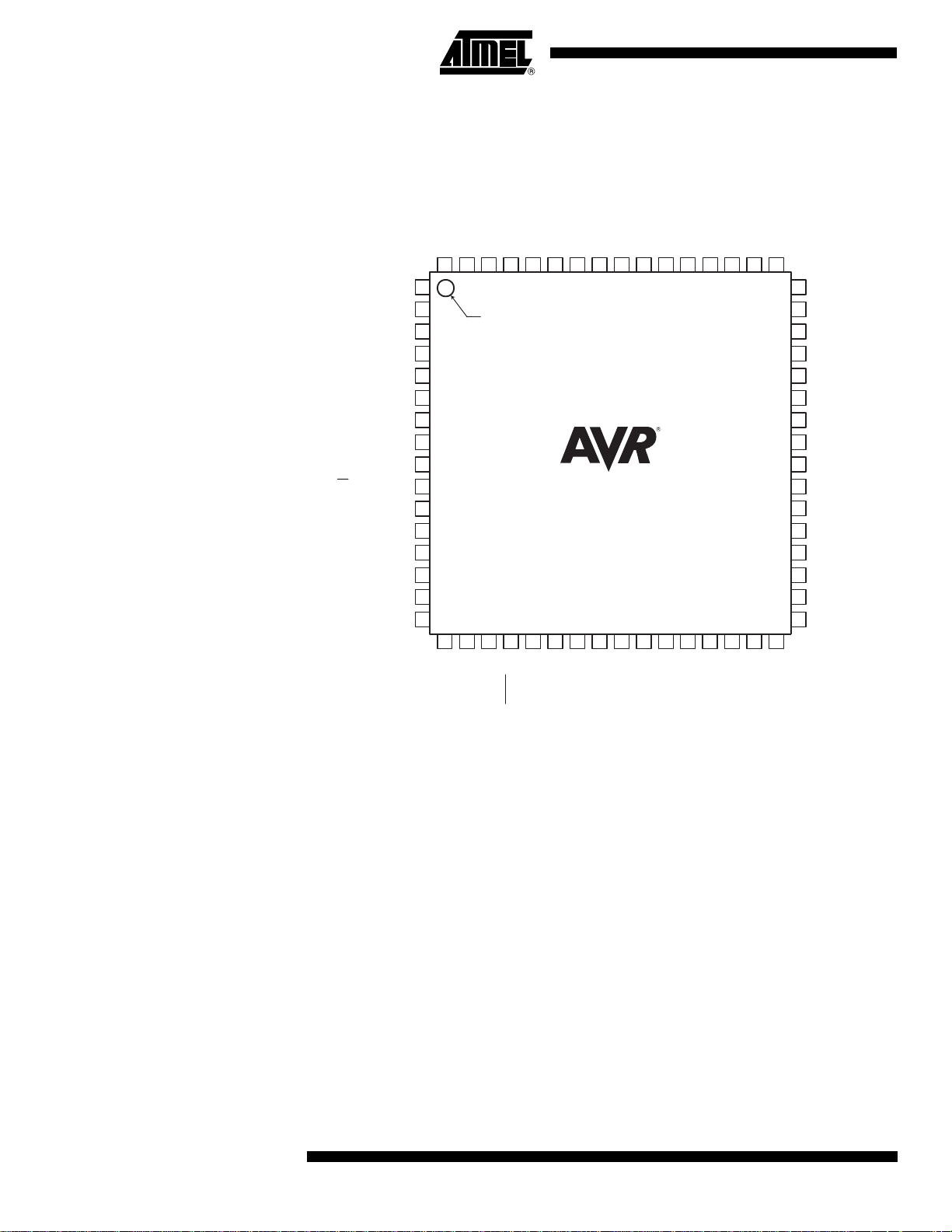
1. Pin Configurations
Figure 1-1. Pinout ATmega165P
DNC
(RXD/PCINT0) PE0
(TXD/PCINT1) PE1
(XCK/AIN0/PCINT2) PE2
(AIN1/PCINT3) PE3
(USCK/SCL/PCINT4) PE4
(DI/SDA/PCINT5) PE5
(DO/PCINT6) PE6
(CLKO/PCINT7) PE7
(SS/PCINT8) PB0
(SCK/PCINT9) PB1
(MOSI/PCINT10) PB2
(MISO/PCINT11) PB3
(OC0A/PCINT12) PB4
(OC1A/PCINT13) PB5
(OC1B/PCINT14) PB6
AVCC
64
1
2
3
4
5
6
7
8
9
10
11
12
13
14
15
16
17
(OC2A/PCINT15) PB7
AREF
GND
63
62
INDEX CORNER
19
(T0) PG4
(T1) PG3
PF0 (ADC0)
PF1 (ADC1)
61
6018592058
21
VCC
RESET/PG5
PF2 (ADC2)
PF3 (ADC3)
PF4 (ADC4/TCK)
PF5 (ADC5/TMS)
57225623552454255326522751
GND
(ICP1) PD0
(TOSC1) XTAL1
(TOSC2) XTAL2
GND
PF7 (ADC7/TDI)
PF6 (ADC6/TDO)
28
PD3
PD2
(INT0) PD1
VCC
29
PD4
PA0
30
PD5
PA1
50
31
PD6
PA2
49
32
PD7
48
47
46
45
44
43
42
41
40
39
38
37
36
35
34
33
PA3
PA4
PA5
PA6
PA7
PG2
PC7
PC6
PC5
PC4
PC3
PC2
PC1
PC0
PG1
PG0
1.1 Disclaimer
2
ATmega165P
Note: The large center pad underneath the QFN/MLF packages is made of metal and internally con-
nected to GND. It should be soldered or glued to the board to ensure good mechanical stability. If
the center pad is left unconnected, the package might loosen from the board.
Typical values contained in this datasheet are based on simulations and characterization of
other AVR microcontrollers manufactured on the same process technology. Min and Max values
will be available after the device is characterized.
8019HS–AVR–11/06
Page 3
ATmega165P
2. Overview
The ATmega165P is a low-power CMOS 8-bit microcontroller based on the AVR enhanced RISC architecture. By executing powerful instructions in a single clock cycle, the ATmega165P achieves throughputs approaching 1 MIPS per MHz
allowing the system designer to optimize power consumption versus processing speed.
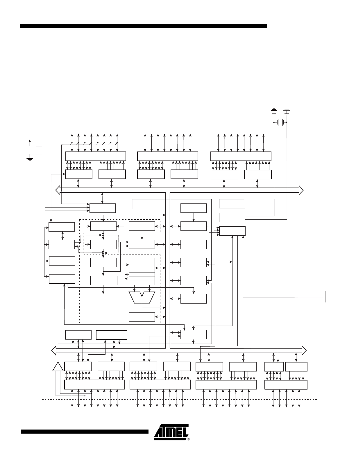
2.1 Block Diagram
Figure 2-1. Block Diagram
AVCC
AREF
VCC
GND
DATA REGISTER
JTAG TAP
ON-CHIP DEBUG
BOUNDARY-
SCAN
PROGRAMMING
LOGIC
PORTF DRIVERS
PORTF
DATA DIR.
REG. PORTF
ADC
PROGRAM
COUNTER
PROGRAM
FLASH
INSTRUCTION
REGISTER
INSTRUCTION
DECODER
CONTROL
LINES
DATA REGISTER
PORTA
STACK
POINTER
SRAM
GENERAL
PURPOSE
REGISTERS
X
Y
Z
ALU
PA0 - PA7PF0 - PF7
PORTA DRIVERS
DATA DIR.
REG. PORTA
8-BIT DATA BUS
INTERNAL
OSCILLATOR
WATCHDOG
TIMER
MCU CONTROL
REGISTER
TIMER/
COUNTERS
INTERRUPT
UNIT
EEPROM
PORTC DRIVERS
DATA REGISTER
PORTC
CALIB. OSC
OSCILLATOR
TIMING AND
CONTROL
PC0 - PC7
DATA DIR.
REG. PORTC
XTAL1
XTAL2
RESET
ANALOG
COMPARATOR
8019HS–AVR–11/06
DATA REGISTER
+
-
AVR CPU
USART
PORTE
UNIVERSAL
SERIAL INTERFACE
DATA DIR.
REG. PORTE
PORTE DRIVERS
STATUS
REGISTER
DATA REGISTER
PORTB
PORTB DRIVERS
PB0 - PB7PE0 - PE7
DATA DIR.
REG. PORTB
SPI
DATA REGISTER
PORTD
REG. PORTD
PORTD DRIVERS
PD0 - PD7
DATA DIR.
DATA REG.
PORTG
PORTG DRIVERS
DATA DIR.
REG. PORTG
PG0 - PG4
3
Page 4

The AVR core combines a rich instruction set with 32 general purpose working registers. All the
32 registers are directly connected to the Arithmetic Logic Unit (ALU), allowing two independent
registers to be accessed in one single instruction executed in one clock cycle. The resulting
architecture is more code efficient while achieving throughputs up to ten times faster than conventional CISC microcontrollers.
The ATmega165P provides the following features: 16K bytes of In-System Programmable Flash
with Read-While-Write capabilities, 512 bytes EEPROM, 1K byte SRAM, 53 general purpose I/O
lines, 32 general purpose working registers, a JTAG interface for Boundary-scan, On-chip
Debugging support and programming, three flexible Timer/Counters with compare modes, internal and external interrupts, a serial programmable USART, Universal Serial Interface with Start
Condition Detector, an 8-channel, 10-bit ADC, a programmable Watchdog Timer with internal
Oscillator, an SPI serial port, and five software selectable power saving modes. The Idle mode
stops the CPU while allowing the SRAM, Timer/Counters, SPI port, and interrupt system to continue functioning. The Power-down mode saves the register contents but freezes the Oscillator,
disabling all other chip functions until the next interrupt or hardware reset. In Power-save mode,
the asynchronous timer continues to run, allowing the user to maintain a timer base while the
rest of the device is sleeping. The ADC Noise Reduction mode stops the CPU and all I/O modules except asynchronous timer and ADC, to minimize switching noise during ADC conversions.
In Standby mode, the crystal/resonator Oscillator is running while the rest of the device is sleeping. This allows very fast start-up combined with low-power consumption.
The device is manufactured using Atmel’s high density non-volatile memory technology. The
On-chip ISP Flash allows the program memory to be reprogrammed In-System through an SPI
serial interface, by a conventional non-volatile memory programmer, or by an On-chip Boot program running on the AVR core. The Boot program can use any interface to download the
application program in the Application Flash memory. Software in the Boot Flash section will
continue to run while the Application Flash section is updated, providing true Read-While-Write
operation. By combining an 8-bit RISC CPU with In-System Self-Programmable Flash on a
monolithic chip, the Atmel ATmega165P is a powerful microcontroller that provides a highly flexible and cost effective solution to many embedded control applications.
The ATmega165P AVR is supported with a full suite of program and system development tools
including: C Compilers, Macro Assemblers, Program Debugger/Simulators, In-Circuit Emulators,
and Evaluation kits.
4
ATmega165P
8019HS–AVR–11/06
Page 5

2.2 Pin Descriptions
2.2.1 VCC
Digital supply voltage.
2.2.2 GND
Ground.
2.2.3 Port A (PA7:PA0)
Port A is an 8-bit bi-directional I/O port with internal pull-up resistors (selected for each bit). The
Port A output buffers have symmetrical drive characteristics with both high sink and source
capability. As inputs, Port A pins that are externally pulled low will source current if the pull-up
resistors are activated. The Port A pins are tri-stated when a reset condition becomes active,
even if the clock is not running.
2.2.4 Port B (PB7:PB0)
Port B is an 8-bit bi-directional I/O port with internal pull-up resistors (selected for each bit). The
Port B output buffers have symmetrical drive characteristics with both high sink and source
capability. As inputs, Port B pins that are externally pulled low will source current if the pull-up
resistors are activated. The Port B pins are tri-stated when a reset condition becomes active,
even if the clock is not running.
ATmega165P
Port B has better driving capabilities than the other ports.
Port B also serves the functions of various special features of the ATmega165P as listed on
”Alternate Functions of Port B” on page 72.
2.2.5 Port C (PC7:PC0)
Port C is an 8-bit bi-directional I/O port with internal pull-up resistors (selected for each bit). The
Port C output buffers have symmetrical drive characteristics with both high sink and source
capability. As inputs, Port C pins that are externally pulled low will source current if the pull-up
resistors are activated. The Port C pins are tri-stated when a reset condition becomes active,
even if the clock is not running.
2.2.6 Port D (PD7:PD0)
Port D is an 8-bit bi-directional I/O port with internal pull-up resistors (selected for each bit). The
Port D output buffers have symmetrical drive characteristics with both high sink and source
capability. As inputs, Port D pins that are externally pulled low will source current if the pull-up
resistors are activated. The Port D pins are tri-stated when a reset condition becomes active,
even if the clock is not running.
Port D also serves the functions of various special features of the ATmega165P as listed on
”Alternate Functions of Port D” on page 75.
2.2.7 Port E (PE7:PE0)
8019HS–AVR–11/06
Port E is an 8-bit bi-directional I/O port with internal pull-up resistors (selected for each bit). The
Port E output buffers have symmetrical drive characteristics with both high sink and source
capability. As inputs, Port E pins that are externally pulled low will source current if the pull-up
5
Page 6

resistors are activated. The Port E pins are tri-stated when a reset condition becomes active,
even if the clock is not running.
Port E also serves the functions of various special features of the ATmega165P as listed on
”Alternate Functions of Port E” on page 76.
2.2.8 Port F (PF7:PF0)
Port F serves as the analog inputs to the A/D Converter.
Port F also serves as an 8-bit bi-directional I/O port, if the A/D Converter is not used. Port pins
can provide internal pull-up resistors (selected for each bit). The Port F output buffers have symmetrical drive characteristics with both high sink and source capability. As inputs, Port F pins
that are externally pulled low will source current if the pull-up resistors are activated. The Port F
pins are tri-stated when a reset condition becomes active, even if the clock is not running. If the
JTAG interface is enabled, the pull-up resistors on pins PF7(TDI), PF5(TMS), and PF4(TCK) will
be activated even if a reset occurs.
Port F also serves the functions of the JTAG interface, see ”Alternate Functions of Port F” on
page 79
2.2.9 Port G (PG5:PG0)
Port G is a 6-bit bi-directional I/O port with internal pull-up resistors (selected for each bit). The
Port G output buffers have symmetrical drive characteristics with both high sink and source
capability. As inputs, Port G pins that are externally pulled low will source current if the pull-up
resistors are activated. The Port G pins are tri-stated when a reset condition becomes active,
even if the clock is not running.
2.2.10 RESET
2.2.11 XTAL1
2.2.12 XTAL2
2.2.13 AVCC
2.2.14 AREF
Port G also serves the functions of various special features of the ATmega165P as listed on
page 81.
Reset input. A low level on this pin for longer than the minimum pulse length will generate a
reset, even if the clock is not running. The minimum pulse length is given in Table 9-1 on page
46. Shorter pulses are not guaranteed to generate a reset.
Input to the inverting Oscillator amplifier and input to the internal clock operating circuit.
Output from the inverting Oscillator amplifier.
AVCC is the supply voltage pin for Port F and the A/D Converter. It should be externally connected to V
, even if the ADC is not used. If the ADC is used, it should be connected to V
CC
CC
through a low-pass filter.
This is the analog reference pin for the A/D Converter.
6
ATmega165P
8019HS–AVR–11/06
Page 7

3. Resources
ATmega165P
A comprehensive set of development tools, application notes and datasheets are available for
download on http://www.atmel.com/avr.
8019HS–AVR–11/06
7
Page 8

4. Register Summary
Address Name Bit 7 Bit 6 Bit 5 Bit 4 Bit 3 Bit 2 Bit 1 Bit 0 Page
(0xFF) Reserved – – – – – – – –
(0xFE) Reserved – – – – – – – –
(0xFD) Reserved – – – – – – – –
(0xFC) Reserved – – – – – – – –
(0xFB) Reserved – – – – – – – –
(0xFA) Reserved – – – – – – – –
(0xF9) Reserved – – – – – – – –
(0xF8) Reserved – – – – – – – –
(0xF7) Reserved – – – – – – – –
(0xF6) Reserved – – – – – – – –
(0xF5) Reserved – – – – – – – –
(0xF4) Reserved – – – – – – – –
(0xF3) Reserved – – – – – – – –
(0xF2) Reserved – – – – – – – –
(0xF1) Reserved – – – – – – – –
(0xF0) Reserved – – – – – – – –
(0xEF) Reserved
(0xEE) Reserved
(0xED) Reserved – – – – – – – –
(0xEC) Reserved – – – – – – – –
(0xEB) Reserved – – – – – – – –
(0xEA) Reserved – – – – – – – –
(0xE9) Reserved – – – – – – – –
(0xE8) Reserved – – – – – – – –
(0xE7) Reserved – – – – – – – –
(0xE6) Reserved – – – – – – – –
(0xE5) Reserved – – – – – – – –
(0xE4) Reserved – – – – – – – –
(0xE3) Reserved – – – – – – – –
(0xE2) Reserved – – – – – – – –
(0xE1) Reserved – – – – – – – –
(0xE0) Reserved – – – – – – – –
(0xDF) Reserved – – – – – – – –
(0xDE) Reserved – – – – – – – –
(0xDD) Reserved – – – – – – – –
(0xDC) Reserved – – – – – – – –
(0xDB) Reserved – – – – – – – –
(0xDA) Reserved – – – – – – – –
(0xD9) Reserved – – – – – – – –
(0xD8) Reserved – – – – – – – –
(0xD7) Reserved
(0xD6) Reserved
(0xD5) Reserved – – – – – – – –
(0xD4) Reserved
(0xD3) Reserved
(0xD2) Reserved
(0xD1) Reserved – – – – – – – –
(0xD0) Reserved
(0xCF) Reserved
(0xCE) Reserved – – – – – – – –
(0xCD) Reserved
(0xCC) Reserved
(0xCB) Reserved – – – – – – – –
(0xCA) Reserved
(0xC9) Reserved
(0xC8) Reserved – – – – – – – –
(0xC7) Reserved
(0xC6) UDR0 USART0 I/O Data Register 185
(0xC5) UBRR0H
(0xC4) UBRR0L USART0 Baud Rate Register Low 189
(0xC3) Reserved
(0xC2) UCSR0C
(0xC1) UCSR0B RXCIE0 TXCIE0 UDRIE0 RXEN0 TXEN0 UCSZ02 RXB80 TXB80 185
(0xC0) UCSR0A RXC0 TXC0 UDRE0 FE0 DOR0 UPE0 U2X0 MPCM0 185
– – – – – – – –
– – – – – – – –
– – – – – – – –
– – – – – – – –
– – – – – – – –
– – – – – – – –
– – – – – – – –
– – – – – – – –
– – – – – – – –
– – – – – – – –
– – – – – – – –
– – – – – – – –
– – – – – – – –
– – – – – – – –
USART0 Baud Rate Register High 189
– – – – – – – –
– UMSEL0 UPM01 UPM00 USBS0 UCSZ01 UCSZ00 UCPOL0 185
8
ATmega165P
8019HS–AVR–11/06
Page 9

ATmega165P
Address Name Bit 7 Bit 6 Bit 5 Bit 4 Bit 3 Bit 2 Bit 1 Bit 0 Page
(0xBF) Reserved – – – – – – – –
(0xBE) Reserved – – – – – – – –
(0xBD) Reserved – – – – – – – –
(0xBC) Reserved – – – – – – – –
(0xBB) Reserved – – – – – – – –
(0xBA) USIDR USI Data Register 202
(0xB9) USISR USISIF USIOIF USIPF USIDC USICNT3 USICNT2 USICNT1 USICNT0 202
(0xB8) USICR USISIE USIOIE USIWM1 USIWM0 USICS1 USICS0 USICLK USITC 203
(0xB7) Reserved – – – – – – –
(0xB6) ASSR – – – EXCLK AS2 TCN2UB OCR2UB TCR2UB 151
(0xB5) Reserved – – – – – – – –
(0xB4) Reserved – – – – – – – –
(0xB3) OCR2A Timer/Counter2 Output Compare Register A 150
(0xB2) TCNT2 Timer/Counter2 (8-bit) 150
(0xB1) Reserved – – – – – – – –
(0xB0) TCCR2A FOC2A WGM20 COM2A1 COM2A0 WGM21 CS22 CS21 CS20 148
(0xAF) Reserved
(0xAE) Reserved
(0xAD) Reserved – – – – – – – –
(0xAC) Reserved
(0xAB) Reserved
(0xAA) Reserved – – – – – – – –
(0xA9) Reserved – – – – – – – –
(0xA8) Reserved – – – – – – – –
(0xA7) Reserved – – – – – – – –
(0xA6) Reserved – – – – – – – –
(0xA5) Reserved – – – – – – – –
(0xA4) Reserved – – – – – – – –
(0xA3) Reserved – – – – – – – –
(0xA2) Reserved – – – – – – – –
(0xA1) Reserved – – – – – – – –
(0xA0) Reserved – – – – – – – –
(0x9F) Reserved – – – – – – – –
(0x9E) Reserved – – – – – – – –
(0x9D) Reserved – – – – – – – –
(0x9C) Reserved – – – – – – – –
(0x9B) Reserved – – – – – – – –
(0x9A) Reserved – – – – – – – –
(0x99) Reserved – – – – – – – –
(0x98) Reserved – – – – – – – –
(0x97) Reserved – – – – – – – –
(0x96) Reserved – – – – – – – –
(0x95) Reserved – – – – – – – –
(0x94) Reserved
(0x93) Reserved
(0x92) Reserved – – – – – – – –
(0x91) Reserved
(0x90) Reserved
(0x8F) Reserved
(0x8E) Reserved – – – – – – – –
(0x8D) Reserved
(0x8C) Reserved
(0x8B) OCR1BH Timer/Counter1 - Output Compare Register B High Byte 127
(0x8A) OCR1BL Timer/Counter1 - Output Compare Register B Low Byte 127
(0x89) OCR1AH Timer/Counter1 - Output Compare Register A High Byte 127
(0x88) OCR1AL Timer/Counter1 - Output Compare Register A Low Byte 127
(0x87) ICR1H Timer/Counter1 - Input Capture Register High Byte 128
(0x86) ICR1L Timer/Counter1 - Input Capture Register Low Byte 128
(0x85) TCNT1H Timer/Counter1 - Counter Register High Byte 127
(0x84) TCNT1L Timer/Counter1 - Counter Register Low Byte 127
(0x83) Reserved
(0x82) TCCR1C FOC1A FOC1B
(0x81) TCCR1B ICNC1 ICES1
(0x80) TCCR1A COM1A1 COM1A0 COM1B1 COM1B0 – – WGM11 WGM10 123
(0x7F) DIDR1
(0x7E) DIDR0 ADC7D ADC6D ADC5D ADC4D ADC3D ADC2D ADC1D ADC0D 227
– – – – – – – –
– – – – – – – –
– – – – – – – –
– – – – – – – –
– – – – – – – –
– – – – – – – –
– – – – – – – –
– – – – – – – –
– – – – – – – –
– – – – – – – –
– – – – – – – –
– – – – – – – –
– – – – – – 126
– WGM13 WGM12 CS12 CS11 CS10 125
– – – – – – AIN1D AIN0D 209
8019HS–AVR–11/06
9
Page 10
Address Name Bit 7 Bit 6 Bit 5 Bit 4 Bit 3 Bit 2 Bit 1 Bit 0 Page
(0x7D) Reserved – – – – – – – –
(0x7C) ADMUX REFS1 REFS0 ADLAR MUX4 MUX3 MUX2 MUX1 MUX0 223
(0x7B) ADCSRB –ACME – – – ADTS2 ADTS1 ADTS0 208, 227
(0x7A) ADCSRA ADEN ADSC ADATE ADIF ADIE ADPS2 ADPS1 ADPS0 225
(0x79) ADCH ADC Data Register High byte 226
(0x78) ADCL ADC Data Register Low byte 226
(0x77) Reserved – – – – – – – –
(0x76) Reserved – – – – – – – –
(0x75) Reserved – – – – – – – –
(0x74) Reserved – – – – – – – –
(0x73) Reserved – – – – – – – –
(0x72) Reserved – – – – – – – –
(0x71) Reserved – – – – – – – –
(0x70) TIMSK2 – – – – – – OCIE2A TOIE2 151
(0x6F) TIMSK1 – –ICIE1– – OCIE1B OCIE1A TOIE1 128
(0x6E) TIMSK0 – – – – – – OCIE0A TOIE0 99
(0x6D) Reserved
(0x6C) PCMSK1 PCINT15 PCINT14 PCINT13 PCINT12 PCINT11 PCINT10 PCINT9 PCINT8 62
(0x6B) PCMSK0 PCINT7 PCINT6 PCINT5 PCINT4 PCINT3 PCINT2 PCINT1 PCINT0 63
(0x6A) Reserved – – – – – – – –
(0x69) EICRA
(0x68) Reserved – – – – – – – –
(0x67) Reserved – – – – – – – –
(0x66) OSCCAL Oscillator Calibration Register 35
(0x65) Reserved – – – – – – – –
(0x64) PRR – – – – PRTIM1 PRSPI PRUSART0 PRADC 43
(0x63) Reserved – – – – – – – –
(0x62) Reserved – – – – – – – –
(0x61) CLKPR CLKPCE – – – CLKPS3 CLKPS2 CLKPS1 CLKPS0 36
(0x60) WDTCR – – – WDCE WDE WDP2 WDP1 WDP0 53
0x3F (0x5F) SREG I T H S V N Z C 11
0x3E (0x5E) SPH – – – – – SP10 SP9 SP8 13
0x3D (0x5D) SPL SP7 SP6 SP5 SP4 SP3 SP2 SP1 SP0 13
0x3C (0x5C) Reserved
0x3B (0x5B) Reserved
0x3A (0x5A) Reserved
0x39 (0x59) Reserved
0x38 (0x58) Reserved
0x37 (0x57) SPMCSR SPMIE RWWSB – RWWSRE BLBSET PGWRT PGERS SPMEN 271
0x36 (0x56) Reserved – – – – – – – –
0x35 (0x55) MCUCR JTD – –PUD– – IVSEL IVCE 59, 83, 256
0x34 (0x54) MCUSR – – – JTRF WDRF BORF EXTRF PORF 256
0x33 (0x53) SMCR – – – –SM2SM1SM0SE 43
0x32 (0x52) Reserved
0x31 (0x51) OCDR
0x30 (0x50) ACSR ACD ACBG ACO ACI ACIE ACIC ACIS1 ACIS0 208
0x2F (0x4F) Reserved
0x2E (0x4E) SPDR SPI Data Register 162
0x2D (0x4D) SPSR SPIF WCOL – – – – – SPI2X 161
0x2C (0x4C) SPCR SPIE SPE DORD MSTR CPOL CPHA SPR1 SPR0 160
0x2B (0x4B) GPIOR2 General Purpose I/O Register 2 27
0x2A (0x4A) GPIOR1 General Purpose I/O Register 1 27
0x29 (0x49) Reserved – – – – – – – –
0x28 (0x48) Reserved
0x27 (0x47) OCR0A Timer/Counter0 Output Compare Register A 99
0x26 (0x46) TCNT0 Timer/Counter0 (8 Bit) 99
0x25 (0x45) Reserved – – – – – – – –
0x24 (0x44) TCCR0A FOC0A WGM00 COM0A1 COM0A0 WGM01 CS02 CS01 CS00 97
0x23 (0x43) GTCCR TSM
0x22 (0x42) EEARH
0x21 (0x41) EEARL EEPROM Address Register Low Byte 25
0x20 (0x40) EEDR EEPROM Data Register 25
0x1F (0x3F) EECR – – – – EERIE EEMWE EEWE EERE 25
0x1E (0x3E) GPIOR0 General Purpose I/O Register 0 27
0x1D (0x3D) EIMSK PCIE1 PCIE0
0x1C (0x3C) EIFR PCIF1 PCIF0
– – – – – – – –
– – – – – –ISC01ISC00 61
– – – – – – – –
IDRD/OCD
– – – – – – – –
– – – – – – – –
– – – – – – –EEAR8 25
OCDR6 OCDR5 OCDR4 OCDR3 OCDR2 OCDR1 OCDR0 234
– – – – – PSR2 PSR10 132, 152
– – – – –INT0 61
– – – – – INTF0 62
10
ATmega165P
8019HS–AVR–11/06
Page 11
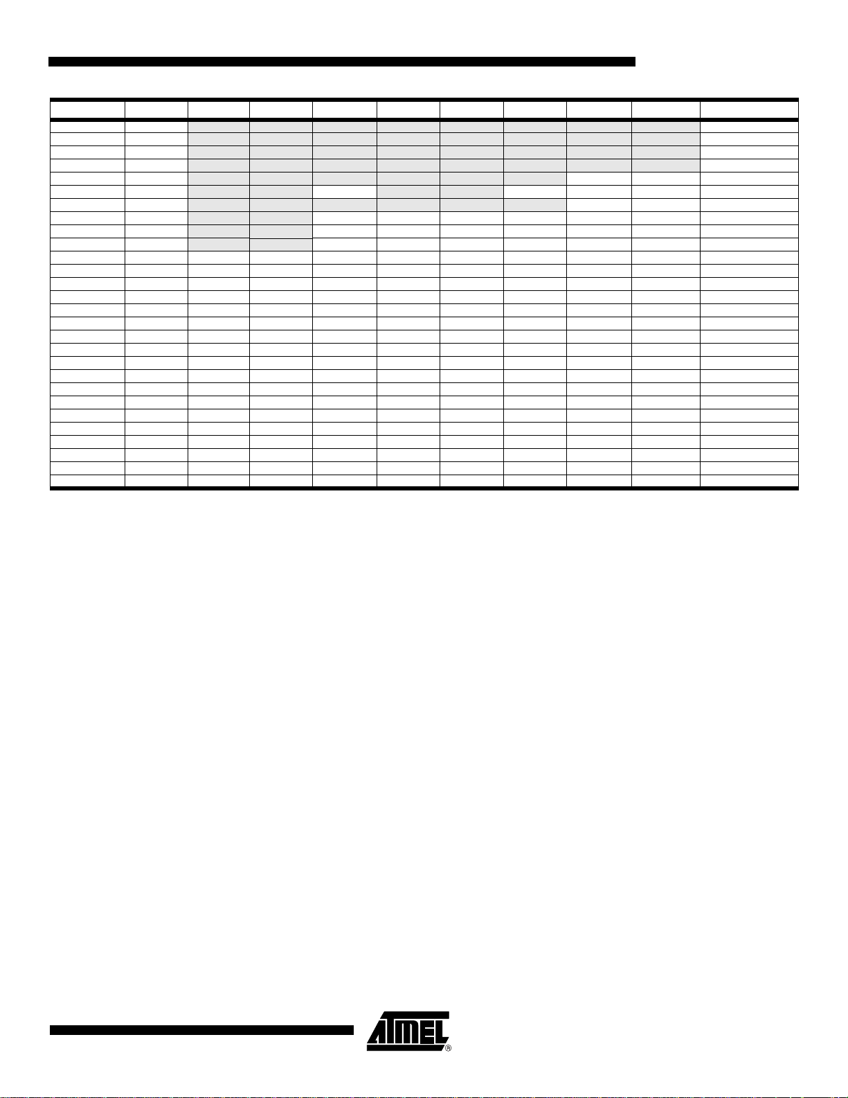
ATmega165P
Address Name Bit 7 Bit 6 Bit 5 Bit 4 Bit 3 Bit 2 Bit 1 Bit 0 Page
0x1B (0x3B) Reserved – – – – – – – –
0x1A (0x3A) Reserved – – – – – – – –
0x19 (0x39) Reserved – – – – – – – –
0x18 (0x38) Reserved – – – – – – – –
0x17 (0x37) TIFR2 – – – – – – OCF2A TOV2 151
0x16 (0x36) TIFR1 – –ICF1– – OCF1B OCF1A TOV1 129
0x15 (0x35) TIFR0 – – – – – – OCF0A TOV0 100
0x14 (0x34) PORTG – – PORTG5 PORTG4 PORTG3 PORTG2 PORTG1 PORTG0 85
0x13 (0x33) DDRG – – DDG5 DDG4 DDG3 DDG2 DDG1 DDG0 85
0x12 (0x32) PING – – PING5 PING4 PING3 PING2 PING1 PING0 85
0x11 (0x31) PORTF PORTF7 PORTF6 PORTF5 PORTF4 PORTF3 PORTF2 PORTF1 PORTF0 85
0x10 (0x30) DDRF DDF7 DDF6 DDF5 DDF4 DDF3 DDF2 DDF1 DDF0 85
0x0F (0x2F) PINF PINF7 PINF6 PINF5 PINF4 PINF3 PINF2 PINF1 PINF0 85
0x0E (0x2E) PORTE PORTE7 PORTE6 PORTE5 PORTE4 PORTE3 PORTE2 PORTE1 PORTE0 84
0x0D (0x2D) DDRE DDE7 DDE6 DDE5 DDE4 DDE3 DDE2 DDE1 DDE0 84
0x0C (0x2C) PINE PINE7 PINE6 PINE5 PINE4 PINE3 PINE2 PINE1 PINE0 85
0x0B (0x2B) PORTD PORTD7 PORTD6 PORTD5 PORTD4 PORTD3 PORTD2 PORTD1 PORTD0 84
0x0A (0x2A) DDRD DDD7 DDD6 DDD5 DDD4 DDD3 DDD2 DDD1 DDD0 84
0x09 (0x29) PIND PIND7 PIND6 PIND5 PIND4 PIND3 PIND2 PIND1 PIND0 84
0x08 (0x28) PORTC PORTC7 PORTC6 PORTC5 PORTC4 PORTC3 PORTC2 PORTC1 PORTC0 84
0x07 (0x27) DDRC DDC7 DDC6 DDC5 DDC4 DDC3 DDC2 DDC1 DDC0 84
0x06 (0x26) PINC PINC7 PINC6 PINC5 PINC4 PINC3 PINC2 PINC1 PINC0 84
0x05 (0x25) PORTB PORTB7 PORTB6 PORTB5 PORTB4 PORTB3 PORTB2 PORTB1 PORTB0 83
0x04 (0x24) DDRB DDB7 DDB6 DDB5 DDB4 DDB3 DDB2 DDB1 DDB0 83
0x03 (0x23) PINB PINB7 PINB6 PINB5 PINB4 PINB3 PINB2 PINB1 PINB0 83
0x02 (0x22) PORTA PORTA7 PORTA6 PORTA5 PORTA4 PORTA3 PORTA2 PORTA1 PORTA0 83
0x01 (0x21) DDRA DDA7 DDA6 DDA5 DDA4 DDA3 DDA2 DDA1 DDA0 83
0x00 (0x20) PINA PINA7 PINA6 PINA5 PINA4 PINA3 PINA2 PINA1 PINA0 83
Note: 1. For compatibility with future devices, reserved bits should be written to zero if accessed. Reserved I/O memory addresses
should never be written.
2. I/O Registers within the address range 0x00 - 0x1F are directly bit-accessible using the SBI and CBI instructions. In these
registers, the value of single bits can be checked by using the SBIS and SBIC instructions.
3. Some of the Status Flags are cleared by writing a logical one to them. Note that, unlike most other AVRs, the CBI and SBI
instructions will only operate on the specified bit, and can therefore be used on registers containing such Status Flags. The
CBI and SBI instructions work with registers 0x00 to 0x1F only.
4. When using the I/O specific commands IN and OUT, the I/O addresses 0x00 - 0x3F must be used. When addressing I/O
Registers as data space using LD and ST instructions, 0x20 must be added to these addresses. The ATmega165P is a complex microcontroller with more peripheral units than can be supported within the 64 location reserved in Opcode for the IN
and OUT instructions. For the Extended I/O space from 0x60 - 0xFF in SRAM, only the ST/STS/STD and LD/LDS/LDD
instructions can be used.
8019HS–AVR–11/06
11
Page 12

5. Instruction Set Summary
Mnemonics Operands Description Operation Flags #Clocks
ARITHMETIC AND LOGIC INSTRUCTIONS
ADD Rd, Rr Add two Registers Rd ← Rd + Rr Z,C,N,V,H 1
ADC Rd, Rr Add with Carry two Registers Rd ← Rd + Rr + C Z,C,N,V,H 1
ADIW Rdl,K Add Immediate to Word Rdh:Rdl ← Rdh:Rdl + K Z,C,N,V,S 2
SUB Rd, Rr Subtract two Registers Rd ← Rd - Rr Z,C,N,V,H 1
SUBI Rd, K Subtract Constant from Register Rd ← Rd - K Z,C,N,V,H 1
SBC Rd, Rr Subtract with Carry two Registers Rd ← Rd - Rr - C Z,C,N,V,H 1
SBCI Rd, K Subtract with Carry Constant from Reg. Rd ← Rd - K - C Z,C,N,V,H 1
SBIW Rdl,K Subtract Immediate from Word Rdh:Rdl ← Rdh:Rdl - K Z,C,N,V,S 2
AND Rd, Rr Logical AND Registers Rd ← Rd • Rr Z,N,V 1
ANDI Rd, K Logical AND Register and Constant Rd ← Rd • K Z,N,V 1
OR Rd, Rr Logical OR Registers Rd ← Rd v Rr Z,N,V 1
ORI Rd, K Logical OR Register and Constant Rd ← Rd v K Z,N,V 1
EOR Rd, Rr Exclusive OR Registers Rd ← Rd ⊕ Rr Z,N,V 1
COM Rd One’s Complement Rd ← 0xFF − Rd Z,C,N,V 1
NEG Rd Two’s Complement Rd ← 0x00 − Rd Z,C,N,V,H 1
SBR Rd,K Set Bit(s) in Register Rd ← Rd v K Z,N,V 1
CBR Rd,K Clear Bit(s) in Register Rd ← Rd • (0xFF - K) Z,N,V 1
INC Rd Increment Rd ← Rd + 1 Z,N,V 1
DEC Rd Decrement Rd ← Rd − 1 Z,N,V 1
TST Rd Test for Zero or Minus Rd ← Rd • Rd Z,N,V 1
CLR Rd Clear Register Rd ← Rd ⊕ Rd Z,N,V 1
SER Rd Set Register Rd ← 0xFF None 1
MUL Rd, Rr Multiply Unsigned R1:R0 ← Rd x Rr Z,C 2
MULS Rd, Rr Multiply Signed R1:R0 ← Rd x Rr Z,C 2
MULSU Rd, Rr Multiply Signed with Unsigned R1:R0 ← Rd x Rr Z,C 2
FMUL Rd, Rr Fractional Multiply Unsigned R1:R0 ← (Rd x Rr) << 1 Z,C 2
FMULS Rd, Rr Fractional Multiply Signed R1:R0 ← (Rd x Rr) << 1 Z,C 2
FMULSU Rd, Rr Fractional Multiply Signed with Unsigned R1:R0 ← (Rd x Rr) << 1 Z,C 2
BRANCH INSTRUCTIONS
RJMP k Relative Jump PC ← PC + k + 1 None 2
IJMP Indirect Jump to (Z) PC ← Z None 2
JMP k Direct Jump PC ← kNone3
RCALL k Relative Subroutine Call PC ← PC + k + 1 None 3
ICALL Indirect Call to (Z) PC ← ZNone3
CALL k Direct Subroutine Call PC ← kNone4
RET Subroutine Return PC ← STACK None 4
RETI Interrupt Return PC ← STACK I 4
CPSE Rd,Rr Compare, Skip if Equal if (Rd = Rr) PC ← PC + 2 or 3 None 1/2/3
CP Rd,Rr Compare Rd − Rr Z, N,V,C,H 1
CPC Rd,Rr Compare with Carry Rd − Rr − C Z, N,V,C,H 1
CPI Rd,K Compare Register with Immediate Rd − K Z, N,V,C,H 1
SBRC Rr, b Skip if Bit in Register Cleared if (Rr(b)=0) PC ← PC + 2 or 3 None 1/2/3
SBRS Rr, b Skip if Bit in Register is Set if (Rr(b)=1) PC ← PC + 2 or 3 None 1/2/3
SBIC P, b Skip if Bit in I/O Register Cleared if (P(b)=0) PC ← PC + 2 or 3 None 1/2/3
SBIS P, b Skip if Bit in I/O Register is Set if (P(b)=1) PC ← PC + 2 or 3 None 1/2/3
BRBS s, k Branch if Status Flag Set if (SREG(s) = 1) then PC←PC+k + 1 None 1/2
BRBC s, k Branch if Status Flag Cleared if (SREG(s) = 0) then PC←PC+k + 1 None 1/2
BREQ k Branch if Equal if (Z = 1) then PC ← PC + k + 1 None 1/2
BRNE k Branch if Not Equal if (Z = 0) then PC ← PC + k + 1 None 1/2
BRCS k Branch if Carry Set if (C = 1) then PC ← PC + k + 1 None 1/2
BRCC k Branch if Carry Cleared if (C = 0) then PC ← PC + k + 1 None 1/2
BRSH k Branch if Same or Higher if (C = 0) then PC ← PC + k + 1 None 1/2
BRLO k Branch if Lower if (C = 1) then PC ← PC + k + 1 None 1/2
BRMI k Branch if Minus if (N = 1) then PC ← PC + k + 1 None 1/2
BRPL k Branch if Plus if (N = 0) then PC ← PC + k + 1 None 1/2
BRGE k Branch if Greater or Equal, Signed if (N ⊕ V= 0) then PC ← PC + k + 1 None 1/2
BRLT k Branch if Less Than Zero, Signed if (N ⊕ V= 1) then PC ← PC + k + 1 None 1/2
BRHS k Branch if Half Carry Flag Set if (H = 1) then PC ← PC + k + 1 None 1/2
BRHC k Branch if Half Carry Flag Cleared if (H = 0) then PC ← PC + k + 1 None 1/2
BRTS k Branch if T Flag Set if (T = 1) then PC ← PC + k + 1 None 1/2
BRTC k Branch if T Flag Cleared if (T = 0) then PC ← PC + k + 1 None 1/2
BRVS k Branch if Overflow Flag is Set if (V = 1) then PC ← PC + k + 1 None 1/2
12
ATmega165P
8019HS–AVR–11/06
Page 13

ATmega165P
Mnemonics Operands Description Operation Flags #Clocks
BRVC k Branch if Overflow Flag is Cleared if (V = 0) then PC ← PC + k + 1 None 1/2
BRIE k Branch if Interrupt Enabled if ( I = 1) then PC ← PC + k + 1 None 1/2
BRID k Branch if Interrupt Disabled if ( I = 0) then PC ← PC + k + 1 None 1/2
BIT AND BIT-TEST INSTRUCTIONS
SBI P,b Set Bit in I/O Register I/O(P,b) ← 1None2
CBI P,b Clear Bit in I/O Register I/O(P,b) ← 0None2
LSL Rd Logical Shift Left Rd(n+1) ← Rd(n), Rd(0) ← 0 Z,C,N,V 1
LSR Rd Logical Shift Right Rd(n) ← Rd(n+1), Rd(7) ← 0 Z,C,N,V 1
ROL Rd Rotate Left Through Carry Rd(0)←C,Rd(n+1)← Rd(n),C←Rd(7) Z,C,N,V 1
ROR Rd Rotate Right Through Carry Rd(7)←C,Rd(n)← Rd(n+1),C←Rd(0) Z,C,N,V 1
ASR Rd Arithmetic Shift Right Rd(n) ← Rd(n+1), n=0..6 Z,C,N,V 1
SWAP Rd Swap Nibbles Rd(3..0)←Rd(7..4),Rd(7..4)←Rd(3..0) None 1
BSET s Flag Set SREG(s) ← 1 SREG(s) 1
BCLR s Flag Clear SREG(s) ← 0 SREG(s) 1
BST Rr, b Bit Store from Register to T T ← Rr(b) T 1
BLD Rd, b Bit load from T to Register Rd(b) ← TNone1
SEC Set Carry C ← 1C1
CLC Clear Carry C ← 0 C 1
SEN Set Negative Flag N ← 1N1
CLN Clear Negative Flag N ← 0 N 1
SEZ Set Zero Flag Z ← 1Z1
CLZ Clear Zero Flag Z ← 0 Z 1
SEI Global Interrupt Enable I ← 1I1
CLI Global Interrupt Disable I ← 0 I 1
SES Set Signed Test Flag S ← 1S1
CLS Clear Signed Test Flag S ← 0 S 1
SEV Set Twos Complement Overflow. V ← 1V1
CLV Clear Twos Complement Overflow V ← 0 V 1
SET Set T in SREG T ← 1T1
CLT Clear T in SREG T ← 0 T 1
SEH Set Half Carry Flag in SREG H ← 1H1
CLH Clear Half Carry Flag in SREG H ← 0 H 1
DATA TRANSFER INSTRUCTIONS
MOV Rd, Rr Move Between Registers Rd ← Rr None 1
MOVW Rd, Rr Copy Register Word
LDI Rd, K Load Immediate Rd ← KNone1
LD Rd, X Load Indirect Rd ← (X) None 2
LD Rd, X+ Load Indirect and Post-Inc. Rd ← (X), X ← X + 1 None 2
LD Rd, - X Load Indirect and Pre-Dec. X ← X - 1, Rd ← (X) None 2
LD Rd, Y Load Indirect Rd ← (Y) None 2
LD Rd, Y+ Load Indirect and Post-Inc. Rd ← (Y), Y ← Y + 1 None 2
LD Rd, - Y Load Indirect and Pre-Dec. Y ← Y - 1, Rd ← (Y) None 2
LDD Rd,Y+q Load Indirect with Displacement Rd ← (Y + q) None 2
LD Rd, Z Load Indirect Rd ← (Z) None 2
LD Rd, Z+ Load Indirect and Post-Inc. Rd ← (Z), Z ← Z+1 None 2
LD Rd, -Z Load Indirect and Pre-Dec. Z ← Z - 1, Rd ← (Z) None 2
LDD Rd, Z+q Load Indirect with Displacement Rd ← (Z + q) None 2
LDS Rd, k Load Direct from SRAM Rd ← (k) None 2
ST X, Rr Store Indirect (X) ← Rr None 2
ST X+, Rr Store Indirect and Post-Inc. (X) ← Rr, X ← X + 1 None 2
ST - X, Rr Store Indirect and Pre-Dec. X ← X - 1, (X) ← Rr None 2
ST Y, Rr Store Indirect (Y) ← Rr None 2
ST Y+, Rr Store Indirect and Post-Inc. (Y) ← Rr, Y ← Y + 1 None 2
ST - Y, Rr Store Indirect and Pre-Dec. Y ← Y - 1, (Y) ← Rr None 2
STD Y+q,Rr Store Indirect with Displacement (Y + q) ← Rr None 2
ST Z, Rr Store Indirect (Z) ← Rr None 2
ST Z+, Rr Store Indirect and Post-Inc. (Z) ← Rr, Z ← Z + 1 None 2
ST -Z, Rr Store Indirect and Pre-Dec. Z ← Z - 1, (Z) ← Rr None 2
STD Z+q,Rr Store Indirect with Displacement (Z + q) ← Rr None 2
STS k, Rr Store Direct to SRAM (k) ← Rr None 2
LPM Load Program Memory R0 ← (Z) None 3
LPM Rd, Z Load Program Memory Rd ← (Z) None 3
LPM Rd, Z+ Load Program Memory and Post-Inc Rd ← (Z), Z ← Z+1 None 3
SPM Store Program Memory (Z) ← R1:R0 None -
IN Rd, P In Port Rd ← PNone1
OUT P, Rr Out Port P ← Rr None 1
Rd+1:Rd ← Rr+1:Rr
None 1
8019HS–AVR–11/06
13
Page 14

Mnemonics Operands Description Operation Flags #Clocks
PUSH Rr Push Register on Stack STACK ← Rr None 2
POP Rd Pop Register from Stack Rd ← STACK None 2
MCU CONTROL INSTRUCTIONS
NOP No Operation None 1
SLEEP Sleep (see specific descr. for Sleep function) None 1
WDR Watchdog Reset (see specific descr. for WDR/timer) None 1
BREAK Break For On-chip Debug Only None N/A
14
ATmega165P
8019HS–AVR–11/06
Page 15
6. Ordering Information
ATmega165P
Speed (MHz)
Notes: 1. This device can also be supplied in wafer form. Please contact your local Atmel sales office for detailed ordering information
2. Pb-free packaging, complies to the European Directive for Restriction of Hazardous Substances (RoHS directive). Also
3. For Speed vs. V
(3)
8 1.8 - 5.5V
16 2.7 - 5.5V
and minimum quantities.
Halide free and fully Green.
Power Supply Ordering Code
, see Figure 26-2 on page 308 and Figure 26-3 on page 308.
CC
ATmega165PV-8AU
ATmega165PV-8MU
ATmega165P-16AU
ATmega165P-16MU
(2)
Package
64A
64M1
64A
64M1
(1)
Operation Range
Industrial
(-40°C to 85°C)
Industrial
0°C to 85°C)
(-4
Package Type
64A 64-Lead, Thin (1.0 mm) Plastic Gull Wing Quad Flat Package (TQFP)
64M1 64-pad, 9 x 9 x 1.0 mm body, lead pitch 0.50 mm, Quad Flat No-Lead/Micro Lead Frame Package (QFN/MLF)
8019HS–AVR–11/06
15
Page 16

7. Packaging Information
7.1 64A
PIN 1
PIN 1 IDENTIFIER
B
e
E1 E
D1
D
C
0˚~7˚
A1
L
Notes: 1. This package conforms to JEDEC reference MS-026, Variation AEB.
2. Dimensions D1 and E1 do not include mold protrusion. Allowable
protrusion is 0.25 mm per side. Dimensions D1 and E1 are maximum
plastic body size dimensions including mold mismatch.
3. Lead coplanarity is 0.10 mm maximum.
A2 A
SYMBOL
COMMON DIMENSIONS
(Unit of Measure = mm)
MIN
A – – 1.20
A1 0.05 – 0.15
A2 0.95 1.00 1.05
D 15.75 16.00 16.25
D1 13.90 14.00 14.10 Note 2
E 15.75 16.00 16.25
E1 13.90 14.00 14.10 Note 2
B 0.30 – 0.45
C 0.09 – 0.20
L 0.45 – 0.75
e 0.80 TYP
NOM
MAX
NOTE
16
2325 Orchard Parkway
R
San Jose, CA 95131
ATmega165P
TITLE
64A, 64-lead, 14 x 14 mm Body Size, 1.0 mm Body Thickness,
0.8 mm Lead Pitch, Thin Profile Plastic Quad Flat Package (TQFP)
10/5/2001
DRAWING NO.
64A
8019HS–AVR–11/06
REV.
B
Page 17

7.2 64M1
D
Marked Pin# 1 ID
ATmega165P
E
SEATING PLANE
C
TOP VIEW
A1
A
K
L
D2
E2
K
b
e
BOTTOM VIEW
1. JEDEC Standard MO-220, (SAW Singulation) Fig. 1, VMMD.
Note:
2. Dimension and tolerance conform to ASMEY14.5M-1994.
Pin #1 Corner
1
2
3
Option A
Option B
Option C
Pin #1
Triangle
Pin #1
Chamfer
(C 0.30)
Pin #1
Notch
(0.20 R)
SIDE VIEW
SYMBOL
A 0.80 0.90 1.00
A1 – 0.02 0.05
b 0.18 0.25 0.30
D
D2 5.20 5.40 5.60
E
E2 5.20 5.40 5.60
e 0.50 BSC
L 0.35 0.40 0.45
K 1.25 1.40 1.55
0.08
C
COMMON DIMENSIONS
(Unit of Measure = mm)
MIN
8.90 9.00 9.10
8.90 9.00 9.10
NOM
MAX
NOTE
R
8019HS–AVR–11/06
2325 Orchard Parkway
San Jose, CA 95131
TITLE
64M1, 64-pad, 9 x 9 x 1.0 mm Body, Lead Pitch 0.50 mm,
5.40 mm Exposed Pad, Micro Lead Frame Package (MLF)
DRAWING NO.
64M1
5/25/06
REV.
G
17
Page 18

8. Errata
8.1 ATmega165P Rev. G
No known errata.
8.2 ATmega165P Rev. A to F
Not sampled.
18
ATmega165P
8019HS–AVR–11/06
Page 19

9. Datasheet Revision History
Please note that the referring page numbers in this section are referring to this document. The
referring revision in this section are referring to the document revision.
9.1 Rev. H 11/06
1. Updated ”Low-frequency Crystal Oscillator” on page 31.
2. Updated Table 26-6 on page 307.
3. Updated note in Table 26-6 on page 307.
9.2 Rev. G 09/06
1. Updated ”Calibrated Internal RC Oscillator” on page 29.
2. Updated ”System Control and Reset” on page 44.
3. Updated Table 7-9 on page 32 and Table 7-10 on page 32.
4. Added note for Table 25-15 on page 286
5. Updated ”Parallel Programming Characteristics” on page 282.
6. Updated ”Electrical Characteristics” on page 301.
ATmega165P
9.3 Rev. F 08/06
9.4 Rev. E 08/06
9.5 Rev. D 07/06
1. Updated Table 1s2-12 on page 80.
2. Updated ”DC Characteristics” on page 304.
1. Updated ”Low-frequency Crystal Oscillator” on page 32.
2. Updated ”Device Identification Register” on page 236.
3. Updated ”Signature Bytes” on page 275.
4. Added Table 25-6 on page 275.
1. Updated ”Register Description for I/O-Ports” on page 83.
2. Updated ”Fast PWM Mode” on page 92.
3. Updated ”Fast PWM Mode” on page 115.
4. Updated Features in ”USI – Universal Serial Interface” on page 194.
5. Added ”Clock speed considerations.” on page 201.
8019HS–AVR–11/06
19
Page 20

9.6 Rev. C 06/06
9.7 Rev. B 04/06
9.8 Rev. A 03/06
6. Updated Table 13-2 on page 97, Table 13-4 on page 98, Table 14-2 on page 123,Table
14-3 on page 124, Table 14-4 on page 125, Table 16-2 on page 148 and Table 16-4 on
page 149.
7. Updated ”UCSRnC – USART Control and Status Register n C” on page 187.
8. Updated ”Register Summary” on page 348.
1. Updated typos.
2. Updated ”Calibrated Internal RC Oscillator” on page 30.
3. Updated ”OSCCAL – Oscillator Calibration Register” on page 36.
4. Added Table 26-5 on page 312.
1. Updated ”Calibrated Internal RC Oscillator” on page 30
2. Updated ”Sleep Modes” on page 38.
1. Initial revision.
20
ATmega165P
8019HS–AVR–11/06
Page 21

Atmel Corporation Atmel Operations
2325 Orchard Parkway
San Jose, CA 95131, USA
Tel: 1(408) 441-0311
Fax: 1(408) 487-2600
Regional Headquarters
Europe
Atmel Sarl
Route des Arsenaux 41
Case Postale 80
CH-1705 Fribourg
Switzerland
Tel: (41) 26-426-5555
Fax: (41) 26-426-5500
Asia
Room 1219
Chinachem Golden Plaza
77 Mody Road Tsimshatsui
East Kowloon
Hong Kong
Tel: (852) 2721-9778
Fax: (852) 2722-1369
Japan
9F, Tonetsu Shinkawa Bldg.
1-24-8 Shinkawa
Chuo-ku, Tokyo 104-0033
Japan
Tel: (81) 3-3523-3551
Fax: (81) 3-3523-7581
Memory
2325 Orchard Parkway
San Jose, CA 95131, USA
Tel: 1(408) 441-0311
Fax: 1(408) 436-4314
Microcontrollers
2325 Orchard Parkway
San Jose, CA 95131, USA
Tel: 1(408) 441-0311
Fax: 1(408) 436-4314
La Chantrerie
BP 70602
44306 Nantes Cedex 3, France
Tel: (33) 2-40-18-18-18
Fax: (33) 2-40-18-19-60
ASIC/ASSP/Smart Cards
Zone Industrielle
13106 Rousset Cedex, France
Tel: (33) 4-42-53-60-00
Fax: (33) 4-42-53-60-01
1150 East Cheyenne Mtn. Blvd.
Colorado Springs, CO 80906, USA
Tel: 1(719) 576-3300
Fax: 1(719) 540-1759
Scottish Enterprise Technology Park
Maxwell Building
East Kilbride G75 0QR, Scotland
Tel: (44) 1355-803-000
Fax: (44) 1355-242-743
RF/Automotive
Theresienstrasse 2
Postfach 3535
74025 Heilbronn, Germany
Tel: (49) 71-31-67-0
Fax: (49) 71-31-67-2340
1150 East Cheyenne Mtn. Blvd.
Colorado Springs, CO 80906, USA
Tel: 1(719) 576-3300
Fax: 1(719) 540-1759
Biometrics/Imaging/Hi-Rel MPU/
High Speed Converters/RF Datacom
Avenue de Rochepleine
BP 123
38521 Saint-Egreve Cedex, France
Tel: (33) 4-76-58-30-00
Fax: (33) 4-76-58-34-80
Literature Requests
www.atmel.com/literature
Disclaimer: The information in this document is provided in connection with Atmel products. No license, express or implied, by estoppel or otherwise, to any
intellectual property right is granted by this document or in connection with the sale of Atmel products. EXCEPT AS SET FORTH IN ATMEL’S TERMS AND CONDI-
TIONS OF SALE LOCATED ON ATMEL’S WEB SITE, ATMEL ASSUMES NO LIABILITY WHATSOEVER AND DISCLAIMS ANY EXPRESS, IMPLIED OR STATUTORY
WARRANTY RELATING TO ITS PRODUCTS INCLUDING, BUT NOT LIMITED TO, THE IMPLIED WARRANTY OF MERCHANTABILITY, FITNESS FOR A PARTICULAR
PURPOSE, OR NON-INFRINGEMENT. IN NO EVENT SHALL ATMEL BE LIABLE FOR ANY DIRECT, INDIRECT, CONSEQUENTIAL, PUNITIVE, SPECIAL OR INCIDENTAL DAMAGES (INCLUDING, WITHOUT LIMITATION, DAMAGES FOR LOSS OF PROFITS, BUSINESS INTERRUPTION, OR LOSS OF INFORMATION) ARISING OUT
OF THE USE OR INABILITY TO USE THIS DOCUMENT, EVEN IF ATMEL HAS BEEN ADVISED OF THE POSSIBILITY OF SUCH DAMAGES. Atmel makes no
representations or warranties with respect to the accuracy or completeness of the contents of this document and reserves the right to make changes to specifications
and product descriptions at any time without notice. Atmel does not make any commitment to update the information contained herein. Unless specifically provided
otherwise, Atmel products are not suitable for, and shall not be used in, automotive applications. Atmel’s products are not intended, authorized, or warranted for use
as components in applications intended to support or sustain life.
© 2006 Atmel Corporation. All rights reserved. AT ME L®, logo and combinations thereof, Everywhere You Are®, AVR®, AVR Studio®, and oth-
ers, are registered trademarks or trademarks of Atmel Corporation or its subsidiaries. Other terms and product names may be trademarks of others.
8019HS–AVR–11/06
 Loading...