

Features
• High-perf ormance, High-density, Electrically-erasable Programmable Logic Device
• Fully Connected Logic Arr ay with 416 Product Terms
• 15 ns Maximum Pin-to-pin Delay for 5V Operation
• 24 Flexible Output Macrocells
– 48 Flip-flop s – Two per Macrocell
–72 Sum Terms
– All Flip-flops, I/O Pins Feed i n Independently
• D- or T-type Flip -flops
• Product Term or Direct Input Pin Clocking
• Registered or Combinatorial Internal Feedback
• Backwar d Com patible with ATV2500B/BQ and ATV2500H Software
• Advanced Electrically-erasable Technology
– Reprogrammable
– 100 % Tested
• 44-lead Surface Mount Package and DIP Pac kage
• Flexible D es i g n: Up to 48 B urie d Fl ip -flops and 24 Combina to r ia l O u tp u ts
Simultaneously
• 8 Synchronous Product Terms
• Individual Asyn chronous Reset per Macr ocell
• OE Control per Macr ocell
• Functionali ty Equi valent to ATV2500B/BQ and ATV2500H
• 2000V ESD Protection
• Security Fuse Feature to Protect the Code
• Commercial and Industrial Temperature Range Offered
• 10 Y ear Data Retention
• Pin Keeper Option
• 200 mA Latch-up Immunity
ATF2500C
CPLD Family
Datasheet
ATF2500C
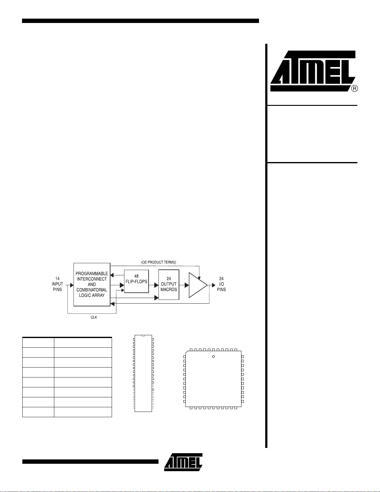
Block Diagram
Pin Configurations
Pin Name Function
IN Logic Inp uts
CLK/IN Pin Clo ck and Input
I/O Bi-directio na l Buf fers
I/O 0,2,4... “Even” I/O Buffers
I/O 1,3,5... “Odd” I/O Buffers
GND Ground
VCC +5V Supply
PLCC/LCC/JLCC
I/O1
I/O0
65432
7
I/O2
8
I/O3
9
I/O4
10
I/O5
11
VCC
12
VCC
13
I/O17
14
I/O16
15
I/O15
16
I/O14
17
I/O13
1819202122232425262728
INININININININ
I/O12
GNDININ
CLK/INININININ
1
4443424140
GND
I/O18
I/O6
39
38
37
36
35
34
33
32
31
30
29
I/O19
I/O7
I/O8
I/O9
I/O10
I/O11
GND
GND
I/O23
I/O22
I/O21
I/O20
CLK/IN
VCC
I/O17
I/O16
I/O15
I/O14
I/O13
I/O12
DIP
1
40
2
IN
3
IN
4
I/O0
5
I/O1
6
I/O2
7
I/O3
8
I/O4
9
I/O5
10
11
12
13
14
15
16
17
IN
18
IN
19
IN
20
IN
IN
39
IN
38
IN
37
IN
36
I/O6
35
I/O7
34
I/O8
33
I/O9
32
I/O10
31
I/O11
30
GND
29
I/O23
28
I/O22
27
I/O21
26
I/O20
25
I/O19
24
I/O18
23
IN
22
IN
21
IN
Note: (PLCC/LCC/JLCC packages) pin 4 and pin 26
GND connections are not required, but are recommended for im proved noise immunity.
Rev. 0777I–PLD–4/03
1

Description The ATF2500C is the highest-density PLD available in a 44-pin package. With its fully con-
nected logic array and flexible macrocell structure, high gate utilization is easily obtainable.
The ATF2500 C is a high-pe rformance CM OS (electric ally-erasable) pro grammab le logic
device (PLD) that utilizes Atmel’s proven electrically-erasable technology.
The ATF2500C is organized around a single universal array. All pins and feedback terms are
always available to every macrocell. Each of the 38 logic pins are array inputs, as are the outputs of each flip-flop.
In the ATF250 0C, four p rod uct term s are inpu t to each sum t erm. Fu rthermore , each macrocell’s three sum terms can be combi ned to provide up t o 12 product terms per sum term with
no performance penalty. Each flip-flop is individually selectable to be either D- or T-type, providing further logic compac tion. Also, 24 of the flip-flo ps may be bypasse d to provide interna l
combinatorial feedback to the logic array.
Product terms provid e individua l clocks and async hronous resets for e ach flip-flop. Th e flipflops may also be ind ividually c onfigured to have direct input pin cl ocking. Ea ch out put has its
own enable product term. Eight synchronous preset product terms serve local groups of either
four or eight flip-flops. Register preload functions are provided to simplify testing. All registers
automatically reset upon power-up.
Using the
ATF2500C
Family’s Many
Advanced
Features
The ATF2500Cs advanced flexibility packs more usable gates into 44 leads than other PLDs.
Some of the ATF2500Cs key features are:
• Fully Connected Logic Array – Each array input is always available to every product
term. This makes logic placement a breeze.
• Selectable D- and T-Type Registers – Each ATF2500C flip-flop can be individually
configured as either D- or T-type. Using the T-type configuration, JK and SR flip-flops are
also easily created. These options allow more efficient product term usage.
• Buried Combinatorial Feedback – Each macrocell’s Q2 register may be bypassed to
feed its input (D/T2) directly back to the logic array. This provides further logic expansion
capability without using precious pin res ourc es.
• Selectable Synchronous/Asynchronous Clocking – Each of the ATF2500Cs flip-flops
has a dedicated clock product term. This removes the constraint that all registers use the
same clock. Buried state machines, counters and registers can all coexist in one device
while running on separate clocks. Individual flip-flop clock source selection fur ther allows
mixing higher performance pin clocking and flexible product term clocking within one
design.
• A Total of 48 Registers – The ATF2500C provides two flip-flops per macrocell – a total of
48. Each register has its own clock and reset terms, as well as its own sum term.
• Independent I/O Pin and Feedback Paths – Each I/O pin on the ATF2500C has a
dedicated input path. Each of the 48 registers has its own feedback term into the array as
well. These features, combined with individual product terms for each I/O’s output enable,
facilitate true bi-directional I/O design.
• Combinable Sum Terms – Each output macrocell’s three sum terms may be combined
into a single term. This provides a fan in of up to 12 product terms per sum term with
speed penalty.
• Programmable Pin-keep er Circuits – These weak feedback latches are useful for bus
interfacing applications. Floating pins can be set to a known state if the Pin-keepers are
enabled.
• User Row (64 bits) – Use to store information such as unit history.
no
2
ATF2500C Family
0777I–PLD–4/03
ATF2500C Family
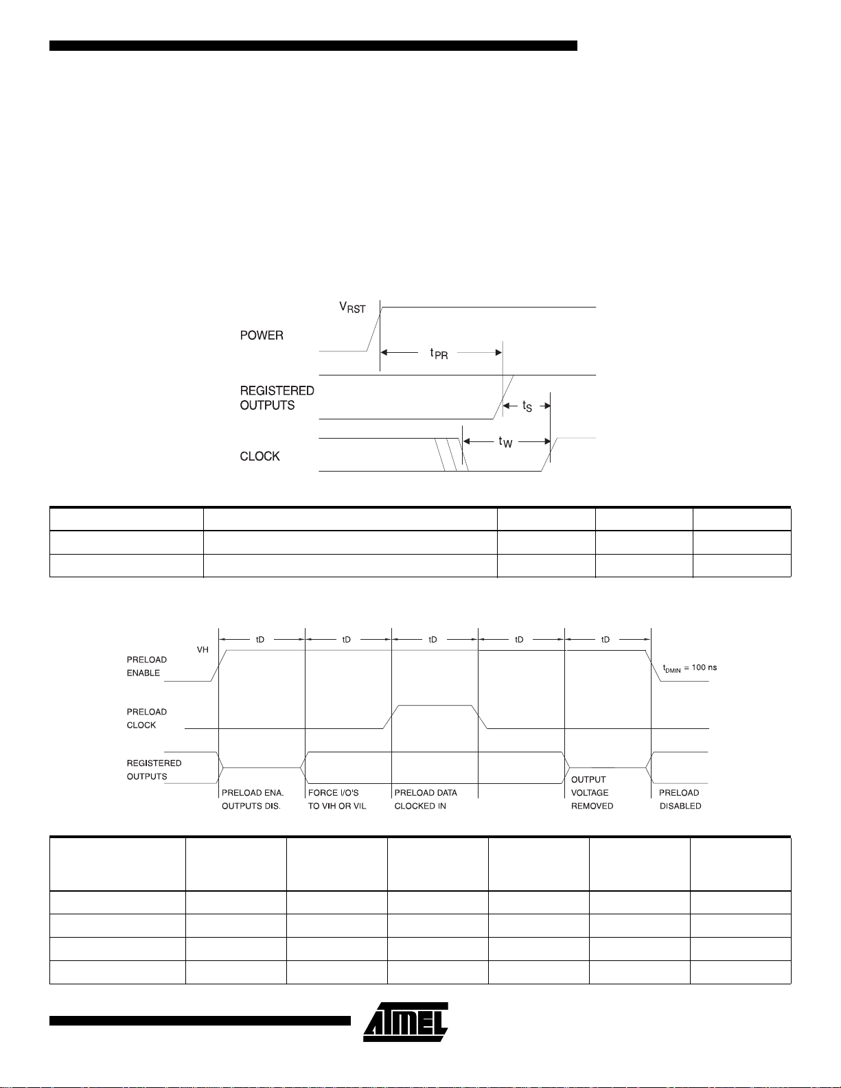
Power-up Reset The registers in the ATF2500Cs are designed to reset during power-up. At a point delayed
slightly f rom V
depend on the polarity of the output buffer.
crossing V
CC
, all registers will be reset to the low state. The output state will
RST
This feature is critical for state as nature of reset and the uncertainty of how V
actually rises
CC
in the system, the following conditions are required:
1. The V
rise must be monotonic,
CC
2. After reset occurs, all input and feedback setup times must be met before driving the
clock pin or terms high, and
3. The clock pin, and any signals from which clock terms are derived, must remain stable
during t
Parameter Description Typ Max Units
t
PR
V
RST
Power-up Reset Time 600 1000 ns
Power-up Reset Voltage 3.8 4.5 V
PR
.
Level Forced on
Odd I/O Pin during
PRELOAD Cyc le
V
IH/VIL
V
IH/VIL
V
IH/VIL
V
IH/VIL
0777I–PLD–4/03
Q Select Pin
State
Low Low High/Low X X X
High Low X High/Low X X
Low Hi gh X X High/Low X
High High X X X High/Low
Even/Odd
Select
Even Q1 State
after Cycle
Even Q2 State
after Cycle
Odd Q1 State
after Cycle
Odd Q2 State
after Cycle
3

Preload and
Observability of
Registered
Outputs
The ATF2500Cs registers are provided with circuitry to allow loading of each register asynchronously w ith either a high or a lo w. This feature w ill simplif y testing since any state can be
forced into the registers to control test sequencing. A V
appropriate register high; a V
tion bit settings.
The PRELOAD state is entered by placing an 10.25V to 10.75V signal on SMP lead 42. When
the preload clock SMP lead 23 is pulsed high, the data on the I/O pins is placed into the 12
registers chosen by the Q select and even/odd select pins.
Register 2 ob ser va bilit y m ode is entered by p lacing an 10. 25V t o 10 .75 V signal on pin/lead 2.
In this m ode , th e cont ents of t he buri ed re gis ter b a nk wi ll a ppe ar on th e as soci ate d ou tpu ts
when the OE control signals are active.
will force it low, independent of the polarity or other configura-
IL
level on the odd I/O pins will force the
IH
Programming
Software
Support
Security Fuse
Usage
Bus-friendly
Pin-keeper
Input and I/O
All family members of the ATF2500C can be designed with Atmel-WinCUPL™. ProC hip
Designer
Additionally, the ATF2500C may be programmed to perform the ATV2500Hs functional subset
(no T-type fl ip-flo ps, pi n clock ing or D/T2 feed back ) using the AT V2 500H JE DE C file. In t his
case, the ATF2500C becomes a direct replacement or speed upgrade for the ATV2500H. The
ATF250 0C ar e d irect re plac em ents for th e ATV 250 0B/BQ a nd the AT V25 00H, includ in g the
lack of extra grounds on P4 and P26.
A single fuse is pro vided to pre vent u nauthori zed copying of AT F2500 C fuse pattern s. On ce
programmed, the outputs will read program m ed dur ing verif y.
The security fuse should be programmed last, as its effect is immediate.
The security fuse also inhibits Preload and Q2 observability.
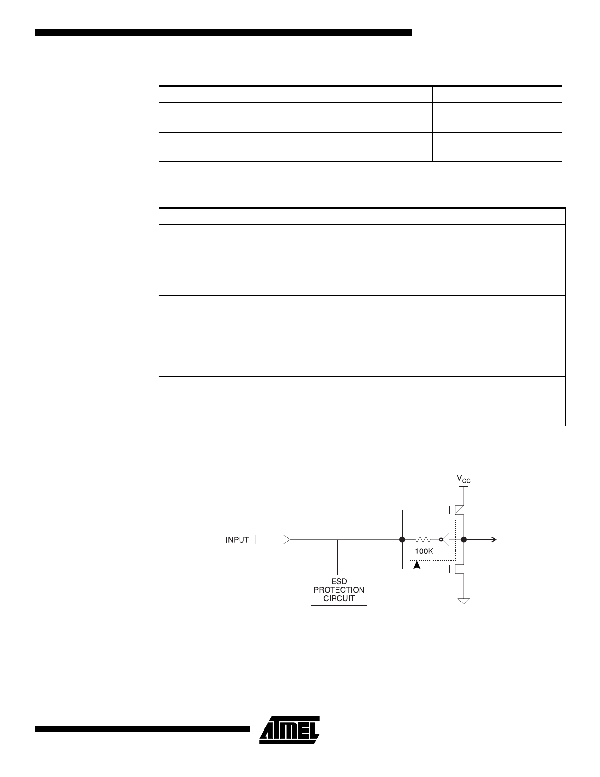
All ATF2500C family members have programmable internal input and I/O pin-keeper circuits.
The default condition, including when using the AT2500C/CQ family to replace the
AT2500B/BQ or AT2500H, is that the pin-keepers are not activated.
When pin-keepers are active, inputs or I/Os not being driven externally will maintain their last
driven state. This ensures that all logic array inputs and device outputs are known states. Pinkeepers are relatively weak active circuits that can be easily overridden by TTL-compatible
drivers (see input and I/O diagrams below).
®
support is expected soon. Check Atmel’s web site for the latest version of ProChip.
Enabling or disab ling of t he pin-ke eper c ircuits is c ontrolle d by the d evice typ e chose n in the
logic compiler de vice selection menu. P lease refer to the S oftw are Com piler Mod e Select ion
table for more details. Once the pin-keeper circuits are disabled, normal termination procedures required for unused inputs and I/Os.
4
ATF2500C Family
0777I–PLD–4/03
Soft ware Compiler Mode Selection
Device Atmel - WinCupL Device Mnemonic Pin-keeper
ATF2500C Family
ATF2500C-DIP
ATF2500C-PLCC
V2500C
V2500CPPK
V2500LCC
V2500CPPKLCC
THIRD PARTY PROGRAMMER SUPPORT
Major Third Party Device Programmers support three types of JEDEC files.
Device Description
V2500 Cross-programming. JEDEC file compatib le with standard V2500
JEDEC file (Total fuses in JEDEC file = 71648). The Progr amm er will
ATF2500C (V2500)
ATF2500C (V2500B)
ATF2500C
automatical ly disable the User row fuses and also disabl e the pin-keeper
feature. The Fuse checksum wil l be the same as the old ATV2500H/L file.
This Device type is recommended for customers that are dir ectly migrating
from an ATV2500H/L device to an ATF2500C device.
V2500B Cross-programming. JEDEC file compatible with standard
V2500B JEDEC file (Total fuses in JEDEC file = 71745). The Programmer
will automatically disable the User row fuses and also disable the pinkeeper feature. The Fuse checksum will be the same as the old
ATV2500B/BQ/BQL/BL file. This Device type is recommended for
customers that are directly migr ati ng from an ATV2500B/BQ/BQL/BL
device to an ATF2500C dev ice.
Programming of User Row bits supported and Pin keeper bit is user programmab le. (Total fuses in JEDEC file = 71816). Thi s is the default
device type and is recommended for users that have Re-compiled their
Source Design files to specifically target the ATF2500C device.
Disabled
Enabled
Disabled
Enabled
Input Diagram
Note: The ATF2500C has 71816 Jedec fuses .
PROGRAMMABLE
OPTION
0777I–PLD–4/03
5
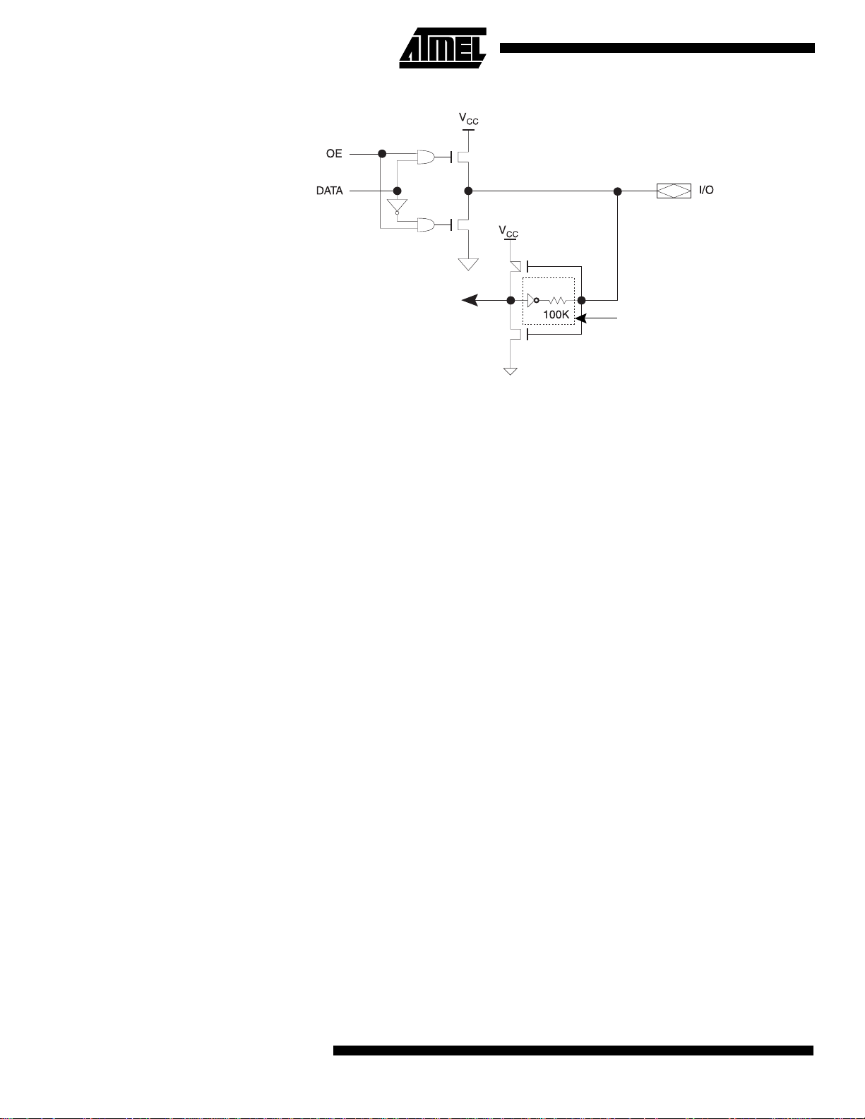
I/O Diagram
INPUT
PROGRAMMABLE
OPTION
Functional
Logic Diagram
Description
The ATF2500C functional logic diagram describes the interconnections between the input,
feedback pins and logic cells. All interconnections are routed through the single global bus.
The ATF2500Cs are straightforward and uniform PLDs. The 24 macrocells are numbered 0
through 23. Each macrocell contai ns 17 AND gates. A ll AND gates have 172 inputs. The five
lower product terms provide AR1, CK1, CK2, AR2, and OE. These are: one asynchronous
reset and clock per flip-flop, and an out put enabl e. The t op 1 2 produc t t erms a re grouped into
three sum terms, which are used as shown in the macrocell diagrams.
Eight synchronous preset terms are distributed in a 2/4 pattern. The first four macrocells share
Preset 0, the next two share Preset 1, and so on, ending with the last two macrocells sharing
Preset 7.
The 14 dedicated in puts and thei r compl em ents use t he num bered positions in the global bus
as shown. E ach m acr ocell prov ide s six inp uts to the glob al bu s: (l eft to r ight ) fe edba ck F 2
true and false, flip-flop Q1 true and false, and the pin true and false. The positions occupied by
these signals in the global bus are the six numbers in the bus diagram next to each macrocell.
Note: 1. Either the flip-fl op input (D/T2) or output (Q2) may be fed bac k in the ATF2500Cs.
(1)
6
ATF2500C Family
0777I–PLD–4/03

Functional Logic Diagram ATF2500C
ATF2500C Family
Notes: 1. Pin 4 and Pin 26 are “ground” connections and are not required for PLCC, LCC and JLCC versions of ATF2500C, making
them compatible with ATV2500H, ATV2500B and ATV2500BQ pinouts.
2. For DIP package, VCC = P10 and GND = P30. For, PLCC, LCC and JLCC packages, VCC = P11 and P12, GND = P33 and
P34, and GND = P4, P26 (See Note 1, above).
0777I–PLD–4/03
7

Output Logic, Registered
(1)
S2 = 0 Terms in
Output ConfigurationS1 S0 D/T1 D/T2
0 0 8 4 Registered (Q1); Q2 FB
(1)
10124
1 1 8 4 Registered (Q1); D/T2 FB
Output
S3
Configur a tion S6 Q1 CLOCK
0Active Low 0CK1
1 Active High 1 CK1 • PIN1
Registered (Q1) ; Q2 FB
Output Logic, Combinatorial
(1)
S4 Register 1 Type S7
0D 0CK2
1T 1CK2 • PIN1
S5 Register 2 Type
0D
1T
S2 = 1 Terms in
Output ConfigurationS5 S1 S0 D/T1 D/T2
X004
X0144
X104
1114
01144
(1)
(1)
(1)
Combinatorial (8 Terms);
4
Q2 FB
Combinatorial (4 Terms);
Q2 FB
Combinatorial (12 Terms);
(1)
4
Q2 FB
Combinatorial (8 Terms);
4
D/T2 FB
Combinatorial (4 Terms);
D/T2 FB
Q2 CLOCK
Note: 1. These four te rms are share d wit h D/T1.
Note: 1. These diagrams show equivalent logic functions, not
necessarily the actual circuit implementation.
8
ATF2500C Family
Clock Option
0777I–PLD–4/03

Absolute Maximum Ratings*
Temperature Under Bias.................................. -40°C to +85°C
Storage Temperature................................... .. -65°C to +150°C
Junction Temperature ............................................. 150°C Max
Voltage on Any Pin with
Respec t to Gr o und ... .. ...................... ... .. ........ . -2 . 0V to +7.0 V
Voltage on Input Pins
with Respect to Ground
Durin g Prog ra m m in g . .. ........ .. ... ....... .. ... ....... ..-2. 0 V to +1 4 .0 V
Programming Voltage with
Respec t to Gr o und ... .. ...................... ... .. ....... -2 . 0 V to +1 4 .0 V
DC and AC Operatin g Conditions
Commercial Industrial
ATF2500C Family
*NOTICE: Stresses bey ond those listed under “Ab solute
Maximum Ratings” may cause permanent damage to the device . This is a stress r ating onl y and
functional operation of th e device at these or any
other conditions beyond those indi cated in the
operational sections of this specification is not
(1)
Note: 1. Minimum voltage is -0.6V DC which may under-
(1)
(1)
implied. Exposure to absolute maximum rati ng
conditions f or e xtended p eriods may af fe ct devi ce
reliability.
shoot to -2.0V for pulses of less than 20 ns.
Maximum output pin voltage i s V
which may overshoot to +7.0V for pulses of less
than 20 ns.
+ 0.75V DC
CC
Operating Temperature
V
Po wer Supply 5V ± 5% 5V ± 10%
CC
0°C - 7 0° C
(Ambient)
-40°C - 85°C
(Ambient)
Pin Capacitance
f = 1 MHz, T = 25°C
C
IN
C
OUT
Note: 1. Typical values for nominal supply voltage. This parameter is onl y sam pled and is not 100% tested.
(1)
Typ Max Units Conditions
46pFV
812pFV
= 0V
IN
OUT
Test Waveforms and Measurement Levels Output Test Load
= 0V
0777I–PLD–4/03
9

AC Waveforms
(1)
Input Pin Clock
AC Waveforms
AC Waveforms
(1)
Product Term Clock
(1)
Combinatorial Outputs and Feedback
Note: 1. Timing measurement reference is 1.5V. Input AC driving levels are 0.0V and 3.0V, unless otherwise specif ied.
10
ATF2500C Family
0777I–PLD–4/03

ATF2500C
ATF2500C DC Characteristics
Symbol Parameter Condition Min Typ Max Units
I
IL
I
LO
I
CC
Input Load Current VIN = -0.1V to VCC + 1V 10 µA
Output Leakage
Current
Power Supply
Current Standby
= -0.1V to VCC + 0.1V 10 µA
V
OUT
V
= MAX,
CC
V
= GND or
IN
V
f = 0 MHz,
CC
ATF2500C
Outputs Open
V
IL
V
IH
V
OL
V
OH
Input Low Voltage M IN ≤ VCC ≤ MAX -0.6 0.8 V
Input High Voltage 2.0 VCC + 0.75 V
I
= 8 mA Com., Ind. 0.5 V
Output Low
Voltage
Output High
Voltage
VIN = VIH or VIL,
V
= 4.5V
CC
V
= MIN
CC
OL
I
= 6 mA Mil. 0.5 V
OL
= -100 µA VCC - 0.3 V
I
OH
I
= -4.0 mA 2.4
OH
Note: 1. See ICC versus frequency characteri zation curves.
ATF2500C AC Characteristics
Symbol Parameter
t
t
t
t
t
t
t
t
t
t
t
PD1
PD2
PD3
PD4
EA1
ER1
EA2
ER2
AW
AP
APF
Input to Non-regist ered Output 15 20 ns
Feedback to Non-registered Output 15 20 ns
Input to Non-regist ered Feedback 11 15 ns
Feedback to Non-registered Feedback 11 15 ns
Input to Output Enable 15 20 ns
Input to Output Disable 15 20 ns
Feedbac k to Output Enable 15 20 ns
Feedbac k to Output Disable 15 20 ns
Asynchronous Reset Width 8 12 ns
Asynchronous Reset to Registered Output 18 22 ns
Asynchronous Reset to Registered Feedback 15 19 ns
Com. 80 110 mA
Ind., Mil. 80 130 mA
-15 -20
UnitsMin Max Min Max
ATF2500C Register AC Characteristics, Input Pin Clock
-15 -20
Symbol Parameter
t
COS
t
CFS
t
SIS
t
SFS
0777I–PLD–4/03
Clock to Output 10 11 ns
Clock to Feedback 0 5 0 6 ns
Input Setup Time 9 14 ns
Feedbac k Setup Time 9 14 ns
Min Max Min Max
Units
11

ATF2500C Register AC Characteristics, Input Pin Clock
-15 -20
Symbol Parameter
t
HS
t
WS
t
PS
Hold Time 0 0 ns
Clock Width 6 7 ns
Clock Period 12 14 ns
External Feedback 1/(t
F
MAXS
Internal Feedback 1/(t
No Feedback 1/(t
t
ARS
Asynchronous Reset/ Preset Recovery Time 12 1 5 ns
+ t
SIS
SFS
)8371MHz
PS
)5240MHz
COS
+ t
)7150MHz
CFS
Min Max Min Max
ATF2500C Register AC Characteristics, Product Term Clock
-15 -20
Units
Symbol Parameter
t
COA
t
CFA
t
SIA
t
SFA
t
HA
t
WA
t
PA
Clock to Output 15 20 ns
Clock to Feedback 5 12 10 16 ns
Input Setup Time 5 10 ns
Feedbac k Setup Time 5 8 ns
Hold Time 5 10 ns
Clock W idth 7. 5 11 ns
Clock Period 15 22 ns
External Feedback 1/(t
F
MAXA
Internal Feedback 1/(t
No Feedback 1/(t
t
ARA
Asynchronous Reset/ Preset Recovery Time 8 12 ns
UnitsMin Max Min Max
+ t
SIA
SFA
)6645MHz
PS
)5033MHz
COA
+ t
)5838MHz
CFA
12
ATF2500C
0777I–PLD–4/03

ATF2500C IV Data 44PLCC
ATF2500C
STAND-BY ICC VS. TEMPERATURE (VCC = 5. 0V)
ATF2500C OUTPUT SOURCE CURRENT VS.
SUPPLY VO L TAGE (V
-10
-20
(mA)
-30
OH
I
-40
4.50 4.75 5.00 5.25 5.50
SUPPLY VOLTAGE (V)
= 2.4V, TA = 25°C)
OH
ATF2500C OUTPUT SINK CURRENT VS.
15
14
13
(mA)
12
OL
I
11
10
SUPPLY VOLTAGE ( V
4.50 4.75 5.00 5.25 5.50
SUPPLY VOLTAGE (V)
= 0.5V, TA = 25°C)
OL
100.0
90.0
80.0
(mA)
CC
70.0
I
60.0
50.0
-40.0 25.0 85.0
TEMPERATURE (°C)
STAND-BY ICC VS.
100.0
90.0
80.0
(mA)
CC
70.0
I
60.0
50.0
4.5 4.8 5.0 5.3 5.5
SUPPLY VOLTAG E (T
SUPPLY VOLTAGE (V)
= 25°C)
A
ATF2500C OUTPUT SOURCE CURRENT VS.
OUTPUT VOLTAGE (V
0.0
-10.0
-20.0
(mA)
OH
I
-30.0
-40.0
0.0 0.5 1.0 1.5 2.0 2.5 3.0 3.5 4.0 4.5 5.0
OUT PUT VO LTAG E (V)
= 5.0V, TA = 25°C)
CC
ATF250 0 C OUTPUT SINK CURRENT VS.
50
40
30
(mA)
20
OL
I
10
0
0.0 0.5 1.0 1.5 2.0 2.5 3.0 3.5 4.0 4.5 5.0
OUTPUT VOLTAGE (V
OUTPUT VOLTAGE (V)
= 5.0V, TA = 25°C)
CC
ATF2500C INPUT CLAMP CURRENT VS.
INPUT VOLTAGE (V
50
0
-50
-100
INPUT
-150
CURRENT (mA)
-200
-1.4 -1.2 -1.0 -0.8 -0.6 -0.4 -0.2 0.0
INPUT VOLTAGE (V)
ATF2500C INPUT CURR ENT VS.
INPUT VOLTA GE (V
40
30
20
10
(mA)
0
CC
I
-10
-20
-30
0.0 0.5 1. 0 1.5 2.0 2.5 3.0 3.5 4.0 4.5 5 . 0
INPUT VOLTAGE (V)
= 5.0V, TA = 25°C)
CC
= 5.0V, TA = 25°C)
CC
0777I–PLD–4/03
13

ATF2500C OUTPUT SOURCE CURRENT VS.
0
OUTPUT VOLTAGE (V
= 5.0V, TA = 25°C)
CC
NORMALI ZED TPD VS. SUPPLY VOLTAGE
= 25°C)
(T
1.2
A
-2
-4
(mA)
OH
I
-6
-8
4.5 4.6 4.7 4.8 4.9 5.0
Outpu t Voltage (V )
ATF2500C OUTPUT SINK CURRENT VS.
30
25
20
15
(mA)
OL
I
10
5
0
0.0 0.1 0.2 0.3 0.4 0.5 0.6 0.7 0.8 0.9 1.0
OUTPUT VO LTAG E ( V
OUTPUT VOLTAGE (V)
= 5.0V, TA = 25°C)
CC
ATF2500C SUPPLY CURRENT VS. SUPPLY
100
90
80
(mA)
70
CC
I
60
50
4.50 4.75 5.00 5.25 5.50
VOLTAGE (Freq. = 0 MHz, T
Supply Voltage (V)
= 25°C)
A
1.1
1.0
NORMALIZED
PD
0.9
T
0.8
4.50 4.75 5.00 5.25 5.50
SUPPLY VOLTAGE (V)
NORMALIZED TPD VS. AMBIENT TEM P (VCC = 5V)
1.1
1.0
0.9
NORMALIZED
PD
T
0.8
-40.0 25.0 85.0
NORM ALI Z ED T
1.1
1.0
NORMALIZED
COS
T
0.9
4.50 4.75 5.00 5.25 5.50
AMBIENT TEMPERATURE (°C)
VS. SUPPLY VO LTAGE
COS
= 25°C)
(T
A
SUPPLY VOLTAGE (V)
14
ATF2500C SUPPLY CURRENT VS.
INPUT FREQ UENCY (V
120
100
(mA)
CC
I
80
60
0102030405060708090
FREQUENCY (MHz)
= 5.0V, TA = 25°C)
CC
ATF2500C
NO RMALIZE D T
1.1
VS. AMBIENT T EMP
COS
= 5V)
(V
CC
1.0
NORMALIZED
0.9
COS
T
0.8
-40.0 25.0 85.0
AMBIENT T EMPER ATURE (°C )
0777I–PLD–4/03

ATF2500C
NOR MALIZED T
1.3
VS. SUPPLY VO LTAGE
COA
= 25°C)
(T
A
1.2
1.1
1.0
NORMALIZED
COA
0.9
T
0.8
4.50 4.75 5.00 5.25 5.50
SUPPLY VOLTAGE (V)
NO R MALIZED T
VS. AM BIENT TEMP
COA
(V
= 5V)
CC
1.1
1.0
0.9
NORMALIZED
COA
T
0.8
-40.0 25.0 85.0
AMBIE NT T EM PERATURE (°C)
NORMALIZED T
1.2
1.1
1.0
NORMALIZED
0.9
SIS
T
0.8
-40.0 25.0 85.0
AMBIE NT TEMPE RATURE ( °C)
NORMALIZ ED T
1.2
1.1
1.0
NORMALIZED
0.9
SIA
T
0.8
4.50 4.75 5.00 5.25 5.50
SUPPLY VOLTAGE (V)
VS. AMBIENT TEMP
SIS
(V
= 5V)
CC
VS. SUPPLY VOLTAGE
SIA
(T
= 25°C)
A
NORMALI ZED T
1.2
1.1
1.0
NORMALIZED
0.9
SIS
T
0.8
4.50 4.75 5.00 5.25 5.50
VS. SU P PL Y VOLTAG E
SIS
= 25°C)
(T
A
SUPPLY VOLTAGE (V)
NORMALIZE D T
1.2
1.1
1.0
NORMALIZED
0.9
SIA
T
0.8
-40.0 25.0 85.0
AMBIENT TEM PERA TURE (° C)
VS. AMBIENT TEMP
SIA
(V
= 5V)
CC
0777I–PLD–4/03
15

Ordering Information
t
PD
(ns)
15 10 52
20 11 40
40P6
44J 44-lead, Plastic J-l eaded Chip Carrier (PLCC)
t
COS
(ns)
40-pin, 0.600" Wide, Plastic, Dual Inline Package (PDIP)
Ext. f
MAXS
(MHz) Ordering Code Package Operation Range
ATF2500C-15JC 44J
ATF2500C-15JI 44J
ATF2500C-20JC
ATF2500C-20PC
ATF2500C-20JI
ATF2500C-20PI
Package Type
44J
40P6
44J
40P6
Commercial
(0°C to 70°C)
Industrial
(-40°C to 85°C)
Commercial
(0°C to 70°C)
Industrial
(-40°C to 85°C)
16
ATF2500C
0777I–PLD–4/03

Packaging Information
44J – PLCC
ATF2500C
1.14(0.045) X 45˚
B
e
0.51(0.020)MAX
45˚ MAX (3X)
Notes: 1. This package conforms to JEDEC reference MS-018, Variation AC.
2. Dimensions D1 and E1 do not include mold protrusion.
Allowable protrusion is .010"(0.254 mm) per side. Dimension D1
and E1 include mold mismatch and are measured at the extreme
material condition at the upper or lower parting line.
3. Lead coplanarity is 0.004" (0.102 mm) maximum.
PIN NO. 1
IDENTIFIER
D1
D
1.14(0.045) X 45˚
E1 E
0.318(0.0125)
0.191(0.0075)
NOM
D2/E2
MAX
B1
A2
A1
A
COMMON DIMENSIONS
(Unit of Measure = mm)
SYMBOL
A 4.191 – 4.572
A1 2.286 – 3.048
A2 0.508 – –
D 17.399 – 17.653
D1 16.510 – 16.662 Note 2
E 17.399 – 17.653
E1 16.510 – 16.662 Note 2
D2/E2 14.986 – 16.002
B 0.660 – 0.813
B1 0.330 – 0.533
e 1.270 TYP
MIN
NOTE
0777I–PLD–4/03
2325 Orchard Parkway
R
San Jose, CA 95131
TITLE
44J, 44-lead, Plastic J-leaded Chip Carrier (PLCC)
DRAWING NO.
44J
10/04/01
REV.
B
17

40P6 – PDIP
PIN
1
E1
A1
B
REF
E
B1
C
L
SEATING PLANE
A
D
e
0º ~ 15º
eB
Notes: 1. This package conforms to JEDEC reference MS-011, Variation AC.
2. Dimensions D and E1 do not include mold Flash or Protrusion.
Mold Flash or Protrusion shall not exceed 0.25 mm (0.010").
TITLE
2325 Orchard Parkway
R
San Jose, CA 95131
40P6, 40-lead (0.600"/15.24 mm Wide) Plastic Dual
Inline Package (PDIP)
COMMON DIMENSIONS
(Unit of Measure = mm)
SYMBOL
A – – 4.826
A1 0.381 – –
D 52.070 – 52.578 Note 2
E 15.240 – 15.875
E1 13.462 – 13.970 Note 2
B 0.356 – 0.559
B1 1.041 – 1.651
L 3.048 – 3.556
C 0.203 – 0.381
eB 15.494 – 17.526
e 2.540 TYP
MIN
NOM
MAX
DRAWING NO.
40P6
NOTE
09/28/01
REV.
B
18
ATF2500C
0777I–PLD–4/03

Atmel Corporation Atmel Operations
2325 Orchard Park way
San Jose, CA 95131
Tel: 1(408) 4 41-0311
Fax: 1(408) 487-260 0
Regional Headquarters
Europe
Atmel Sa rl
Route des Ars enau x 41
Case Postale 8 0
CH-1705 Fri bourg
Switzerland
Tel: (41) 26-4 26-55 55
Fax: (41) 26 -426-550 0
Asia
Room 121 9
Chinachem Gold en Plaza
77 Mody Ro ad Tsims hatsu i
East Kowloon
Hong Kong
Tel: (852) 27 21-9778
Fax: (852) 2 722-136 9
Japan
9F, Tonetsu Sh inkaw a Bl dg.
1-24-8 Shi nkawa
Chuo-ku, Tok yo 10 4-0033
Japan
Tel: (81) 3-35 23-35 51
Fax: (81) 3-3 523-758 1
Memory
2325 Orch ard Parkw ay
San Jose, C A 95131
Tel: 1(408 ) 441-031 1
Fax: 1(408) 43 6-43 14
Microcontrollers
2325 Orch ard Parkw ay
San Jose, C A 95131
Tel: 1(408 ) 441-031 1
Fax: 1(408) 43 6-43 14
La Chantrer ie
BP 70602
44306 Na ntes Cede x 3, Fra nce
Tel: (33) 2-4 0-18 -18-18
Fax: (33) 2-40-18-19-60
ASIC/ASSP/Smart Cards
Zone In dustrielle
13106 Rousse t Ced ex, France
Tel: (33) 4-4 2-53 -60-00
Fax: (33) 4-42-53-60-01
1150 East C heyenn e Mtn. Blvd.
Colorado Sp rings, CO 8 0906
Tel: 1(719 ) 576-330 0
Fax: 1(719) 54 0-17 59
Scottish Enterprise Technology Park
Maxwell Building
East Kilbrid e G7 5 0QR, S cotlan d
Tel: (44) 13 55-803- 000
Fax: (44) 1355 -242 -743
RF/Automotive
Theresienstrasse 2
Postfach 3535
74025 Heilbr onn, Ge rmany
Tel: (49) 71-31-67-0
Fax: (49) 71 -31-67- 2340
1150 East Ch eyenne M tn. B lvd.
Colorado Spr ings, CO 80 906
Tel: 1(719) 57 6-3300
Fax: 1(719) 540-1759
Biometrics/Imaging/Hi-Rel MPU/
High Speed Converters/RF Datacom
Avenue de R ocheplei ne
BP 123
38521 Saint- Egreve Cedex, France
Tel: (33) 4-76-58-30-00
Fax: (33) 4-7 6-58-3 4-80
e-mail
literature@atmel.com
Web Site
http://www.atmel.com
Disclaimer: Atmel Corporation makes no warranty for the use of its products, other than those expressly contained in the Company’s standard
warranty which is detailed in Atmel’s Terms and Conditions located on the Company’s web site. The Company assumes no responsibility for any
errors which may appear in this document, reserves the right to change devices or specifications detailed herein at any time without notice, and
does no t make any com mitment to u pdate the informat ion contai ned herei n. No licen ses to paten ts or othe r intellect ual proper ty of Atmel are
granted by th e Com pany in conn ecti on w ith t he sale of A tme l pr oduc ts, exp ressl y or by im pli catio n. Atme l’s pro duct s ar e no t aut ho rized for us e
as critical components in life support devices or systems.
© Atme l Corporation 2003. All rights reserved. Atme l
are the r eg is tered trademar k s, an d A t me l- W in C U PL™ is the trademark of Atmel Corporation or its subsidiaries.
Other terms and product names may be the trademarks of others.
®
and combinations thereof, and ProChip Designer
®
Printe d on rec ycled pape r.
0777I–4/03/0M

Atmel Corporation Atmel Operations
2325 Orchard Park way
San Jose, CA 95131
Tel: 1(408) 4 41-0311
Fax: 1(408) 487-260 0
Regional Headquarters
Europe
Atmel Sa rl
Route des Ars enau x 41
Case Postale 8 0
CH-1705 Fri bourg
Switzerland
Tel: (41) 26-4 26-55 55
Fax: (41) 26 -426-550 0
Asia
Room 121 9
Chinachem Gold en Plaza
77 Mody Ro ad Tsims hatsu i
East Kowloon
Hong Kong
Tel: (852) 27 21-9778
Fax: (852) 2 722-136 9
Japan
9F, Tonetsu Sh inkaw a Bl dg.
1-24-8 Shi nkawa
Chuo-ku, Tok yo 10 4-0033
Japan
Tel: (81) 3-35 23-35 51
Fax: (81) 3-3 523-758 1
Memory
2325 Orch ard Parkw ay
San Jose, C A 95131
Tel: 1(408 ) 441-031 1
Fax: 1(408) 43 6-43 14
Microcontrollers
2325 Orch ard Parkw ay
San Jose, C A 95131
Tel: 1(408 ) 441-031 1
Fax: 1(408) 43 6-43 14
La Chantrer ie
BP 70602
44306 Na ntes Cede x 3, Fra nce
Tel: (33) 2-4 0-18 -18-18
Fax: (33) 2-40-18-19-60
ASIC/ASSP/Smart Cards
Zone In dustrielle
13106 Rousse t Ced ex, France
Tel: (33) 4-4 2-53 -60-00
Fax: (33) 4-42-53-60-01
1150 East C heyenn e Mtn. Blvd.
Colorado Sp rings, CO 8 0906
Tel: 1(719 ) 576-330 0
Fax: 1(719) 54 0-17 59
Scottish Enterprise Technology Park
Maxwell Building
East Kilbrid e G7 5 0QR, S cotlan d
Tel: (44) 13 55-803- 000
Fax: (44) 1355 -242 -743
RF/Automotive
Theresienstrasse 2
Postfach 3535
74025 Heilbr onn, Ge rmany
Tel: (49) 71-31-67-0
Fax: (49) 71 -31-67- 2340
1150 East Ch eyenne M tn. B lvd.
Colorado Spr ings, CO 80 906
Tel: 1(719) 57 6-3300
Fax: 1(719) 540-1759
Biometrics/Imaging/Hi-Rel MPU/
High Speed Converters/RF Datacom
Avenue de R ocheplei ne
BP 123
38521 Saint- Egreve Cedex, France
Tel: (33) 4-76-58-30-00
Fax: (33) 4-7 6-58-3 4-80
e-mail
literature@atmel.com
Web Site
http://www.atmel.com
Disclaimer: Atmel Corporation makes no warranty for the use of its products, other than those expressly contained in the Company’s standard
warranty which is detailed in Atmel’s Terms and Conditions located on the Company’s web site. The Company assumes no responsibility for any
errors which may appear in this document, reserves the right to change devices or specifications detailed herein at any time without notice, and
does no t make any com mitment to u pdate the informat ion contai ned herei n. No licen ses to paten ts or othe r intellect ual proper ty of Atmel are
granted by th e Com pany in conn ecti on w ith t he sale of A tme l pr oduc ts, exp ressl y or by im pli catio n. Atme l’s pro duct s ar e no t aut ho rized for us e
as critical components in life support devices or systems.
Printe d on rec ycled pape r.
 Loading...