


Features
• Industry-standard Architecture
• 12 ns Maximum Pin-to-pin Delay
• Zero Power – 25 µA Maximum Standby Power (Input Transition Detection)
• CMOS and TTL Compatible Inputs and Outputs
• Advanced Electrically-erasableTechnology
– Reprogrammable
– 100% Tested
• Latch Feature Holds Inputs to Previous Logic State
• High-reliability CMOS Process
– 20 Year Data Retention
– 100 Erase/Write Cycles
– 2,000V ESD Protection
– 200 mA Latchup Immunity
• Commercial and Industrial Temperature Ranges
• Dual-in-line and Surface Mount Standard Pinouts
• PCI Compliant
• Green Package Options (Pb/Halide-free/RoHS Compliant) Available
1. Desscription
The ATF22V10CZ/CQZ is a high-performance CMOS (electrically-erasable)
programmable logic device (PLD) which utilizes Atmel’s proven electrically-erasable
Flash memory technology. Speeds down to 12 ns with zero standby power dissipation
are offered. All speed ranges are specified over the full 5V ±10% range for industrial
temperature ranges; 5V ±5% for commercial range 5-volt devices. The
ATF22V10CZ/CQZ provides a low voltage and edge-sensing “zero” power CMOS
PLD solution with “zero” standby power (5 µA typical). The ATF22V10CZ/CQZ provides a “zero” power CMOS PLD solution with 5V operating voltages, powering down
automatically to the zero power-mode through Atmel’s patented Input Transition
Detection (ITD) circuitry when the device is idle, offering “zero” (25 µA worst case)
standby power. This feature allows the user to manage total system power to meet
specific application requirements and enhance reliability. Pin “keeper” circuits on input
and output pins eliminate static power consumed by pull-up resistors. The “CQZ” combines the low high-frequency I
The ATF22V10CZ/CQZ incorporates a superset of the generic architectures, which
allows direct replacement of the 22V10 family and most 24-pin combinatorial PLDs.
Ten outputs are each allocated 8 to 16 product terms. Three different modes of operation, configured automatically with software, allow highly complex logic functions to be
realized.
of the “Q” design with the “Z” feature.
CC
Highperformance
EE PLD
ATF22V10CZ
ATF22V10CQZ
0778J–PLD–11/07
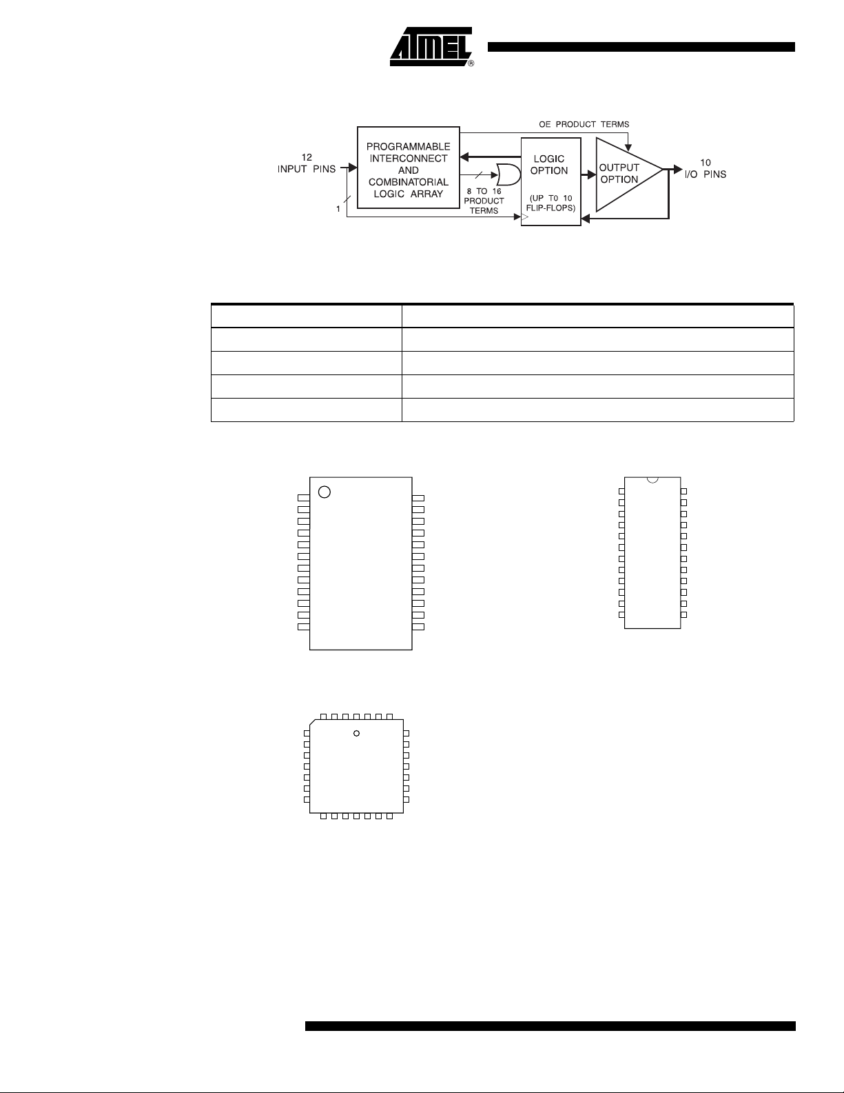
Figure 1-1. Block Diagram
1
2
3
4
5
6
7
8
9
10
11
12
24
23
22
21
20
19
18
17
16
15
14
13
CLK/IN
IN
IN
IN
IN
IN
IN
IN
IN
IN
IN
GND
VCC
I/O
I/O
I/O
I/O
I/O
I/O
I/O
I/O
I/O
I/O
IN
1
2
3
4
5
6
7
8
9
10
11
12
24
23
22
21
20
19
18
17
16
15
14
13
CLK/IN
IN
IN
IN
IN
IN
IN
IN
IN
IN
IN
GND
VCC
I/O
I/O
I/O
I/O
I/O
I/O
I/O
I/O
I/O
I/O
IN
5
6
7
8
9
10
11
25
24
23
22
21
20
19
IN
IN
IN
GND*
IN
IN
IN
I/O
I/O
I/O
GND*
I/O
I/O
I/O
432
1
282726
12131415161718
IN
IN
GND
GND*
IN
I/O
I/O
ININCLK/IN
VCC*
VCC
I/O
I/O
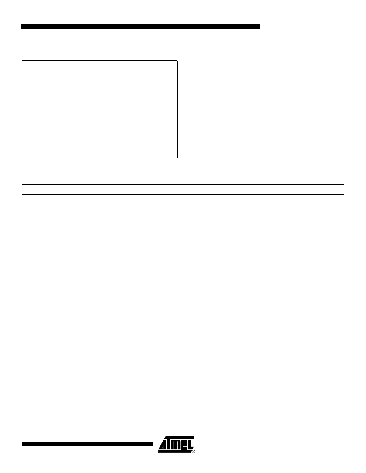
2. Pin Configurations
Table 2-1. Pin Configurations (All Pinouts Top View)
Pin Name Function
CLK Clock
IN Logic Inputs
I/O Bi-directional Buffers
VCC +5V Supply
Figure 2-1. TSSOP Figure 2-2. DIP/SOIC
2
Figure 2-3. PLCC
Note: For PLCC, P1, P8, P15 and P22 can be
left unconnected. For superior performance, connect VCC to pin 1 and GND
to 8, 15, and 22.
ATF22V10C(Q)Z
0778J–PLD–11/07
ATF22V10C(Q)Z
3. Absolute Maximum Ratings*
Temperature Under Bias.................................. -40°C to +85°C
Storage Temperature ..................................... -65°C to +150°C
Voltage on Any Pin with
Respect to Ground .........................................-2.0V to +7.0V
Voltage on Input Pins
with Respect to Ground
During Programming.....................................-2.0V to +14.0V
Programming Voltage with
Respect to Ground .......................................-2.0V to +14.0V
(1)
(1)
(1)
4. DC and AC Operating Conditions
Commercial Industrial
Operating Temperature (Ambient) 0°C - 70°C-40°C - 85°C
*NOTICE: Stresses beyond those listed under “Absolute
Maximum Ratings” may cause permanent damage to the device. This is a stress rating only and
functional operation of the device at these or any
other conditions beyond those indicated in the
operational sections of this specification is not
implied. Exposure to absolute maximum rating
conditions for extended periods may affect device
reliability.
Note: 1. Minimum voltage is -0.6V DC, which may under-
shoot to -2.0V for pulses of less than 20 ns.
Maximum output pin voltage is V
which may overshoot to 7.0V for pulses of less
than 20 ns.
+ 0.75V DC,
CC
VCC Power Supply 5V ± 5% 5V ± 10%
0778J–PLD–11/07
3
4.1 DC Characteristics
Symbol Parameter Condition Min Typ Max Units
I
IL
I
IH
Input or I/O Low
Leakage Current
Input or I/O High
Leakage Current
0 ≤ VIN ≤ V
IN
≤ V
3.5 ≤ V
(Max)
IL
CC
-10 µA
10 µA
CZ-12, 15 Com 90 150 mA
= Max
V
I
CC
Clocked Power
Supply Current
CC
Outputs Open,
f = 15 MHz
CZ-15 Ind 90 180 mA
CQZ-20 Com 40 60 mA
CQZ-20 Ind 40 80 mA
CZ-12, 15 Com 5 25 µA
= Max
V
I
SB
Power Supply Current,
Standby
CC
= MAX
V
IN
Outputs Open
CZ-15 Ind 5 50 µA
CQZ-20 Com 5 25 µA
CQZ-20 Ind 5 50 µA
(1)
I
OS
V
IL
V
IH
V
OL
Output Short Circuit
Current
V
= 0.5V -130 mA
OUT
Input Low Voltage -0.5 0.8 V
Input High Voltage 2.0 VCC + 0.75 V
V
= VIH or V
Output Low Voltage
IN
VCC = Min,
IL
0.5 V
IOL = 16 mA
V
= VIH or V
V
OH
Output High Voltage
V
IN
CCIO
= Min,
IL
2.4 V
IOH = -4.0 mA
Note: 1. Not more than one output at a time should be shorted. Duration of short circuit test should not exceed 30 sec.
4
ATF22V10C(Q)Z
0778J–PLD–11/07
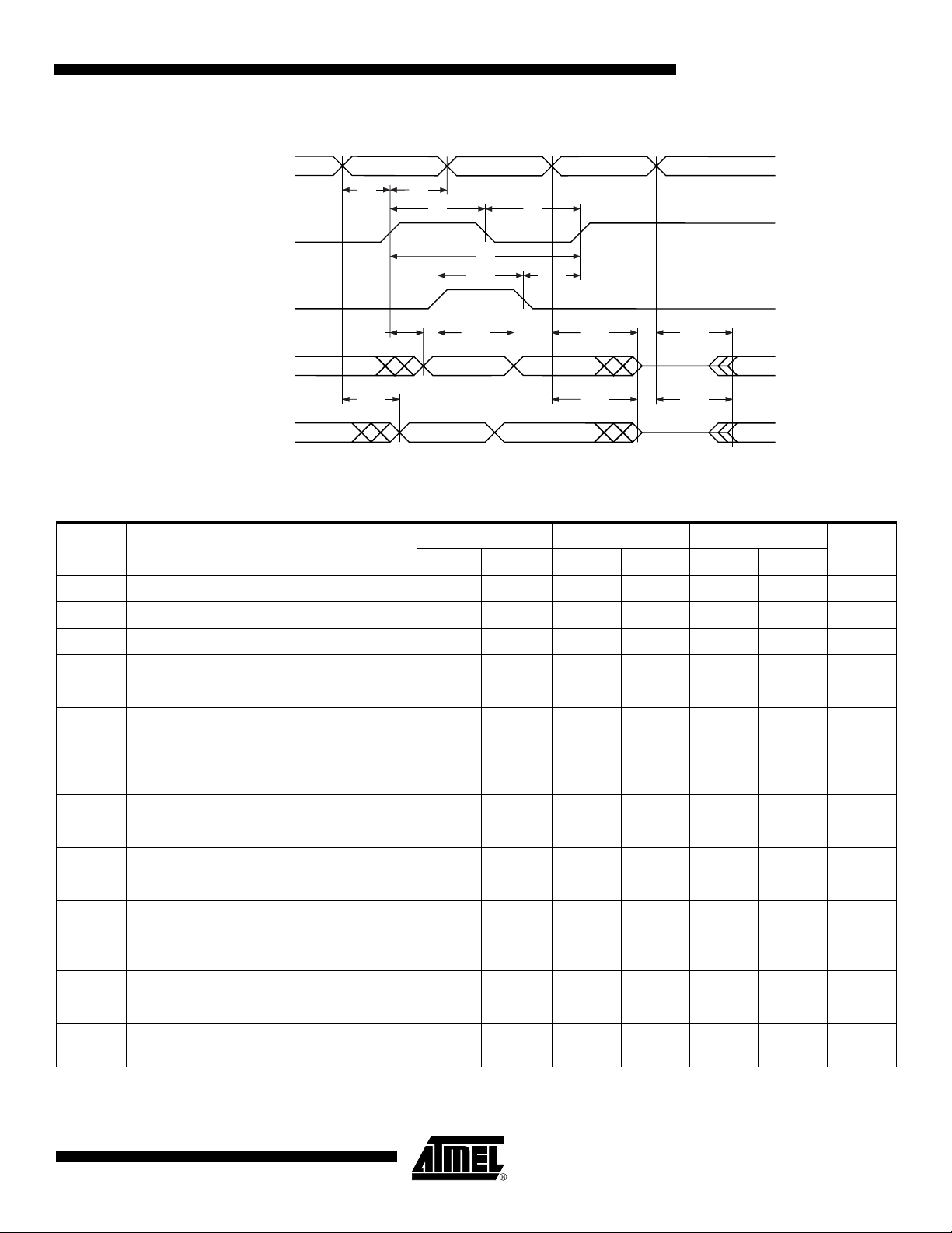
4.2 AC Waveforms
INPUTS, I/O
REG. FEEDBACK
SYNCH. PRESET
CP
ASYNCH. RESET
REGISTERED
OUTPUTS
COMBINATORIAL
OUTPUTS
VALID VALID
VALID
VALID
VALID
VALID
OUTPUT
DISABLED
OUTPUT
DISABLED
tS
tH
tW tW
tP
tAR
tAW
tAPtCO
tPD
tER tEA
tEAtER
ATF22V10C(Q)Z
4.3 AC Characteristics
Symbol Parameter
t
PD
t
CF
t
CO
t
S
t
H
t
W
f
MAX
t
EA
t
ER
t
PZX
t
PXZ
t
AP
t
SP
t
AW
t
AR
t
SPR
Note: 1. See ordering information for valid part numbers.
(1)
-12 -15 -20
UnitsMin Max Min Max Min Max
Input or Feedback to Non-registered Output 3 12 3 15 3 20 ns
Clock to Feedback 6 4.5 8 ns
Clock to Output 2 8 2 8 2 12 ns
Input or Feedback Setup Time 10 10 14 ns
Input Hold Time 0 0 0 ns
Clock Width 6 6 10 ns
External Feedback 1/(tS + tCO)
Internal Feedback 1/(t
+ tCF)
S
No Feedback 1/(tP)
55.5
62
83.3
55.5
69
83.3
38.5
45.5
50.0
MHz
MHz
MHz
Input to Output Enable - Product Term 3 12 3 15 3 20 ns
Input to Output Disable - Product Term 2 15 3 15 3 20 ns
OE Pin to Output Enable 2 12 2 15 2 20 ns
OE Pin to Output Disable 2 15 2 15 2 20 ns
Input or I/O to Asynchronous Reset of
Register
310315322ns
Setup Time, Synchronous Preset 10 10 14 ns
Asynchronous Reset Width 7 8 20 ns
Asynchronous Reset Recovery Time 5 6 20 ns
Synchronous Preset to Clock Recovery
Time
10 10 14 ns
0778J–PLD–11/07
5
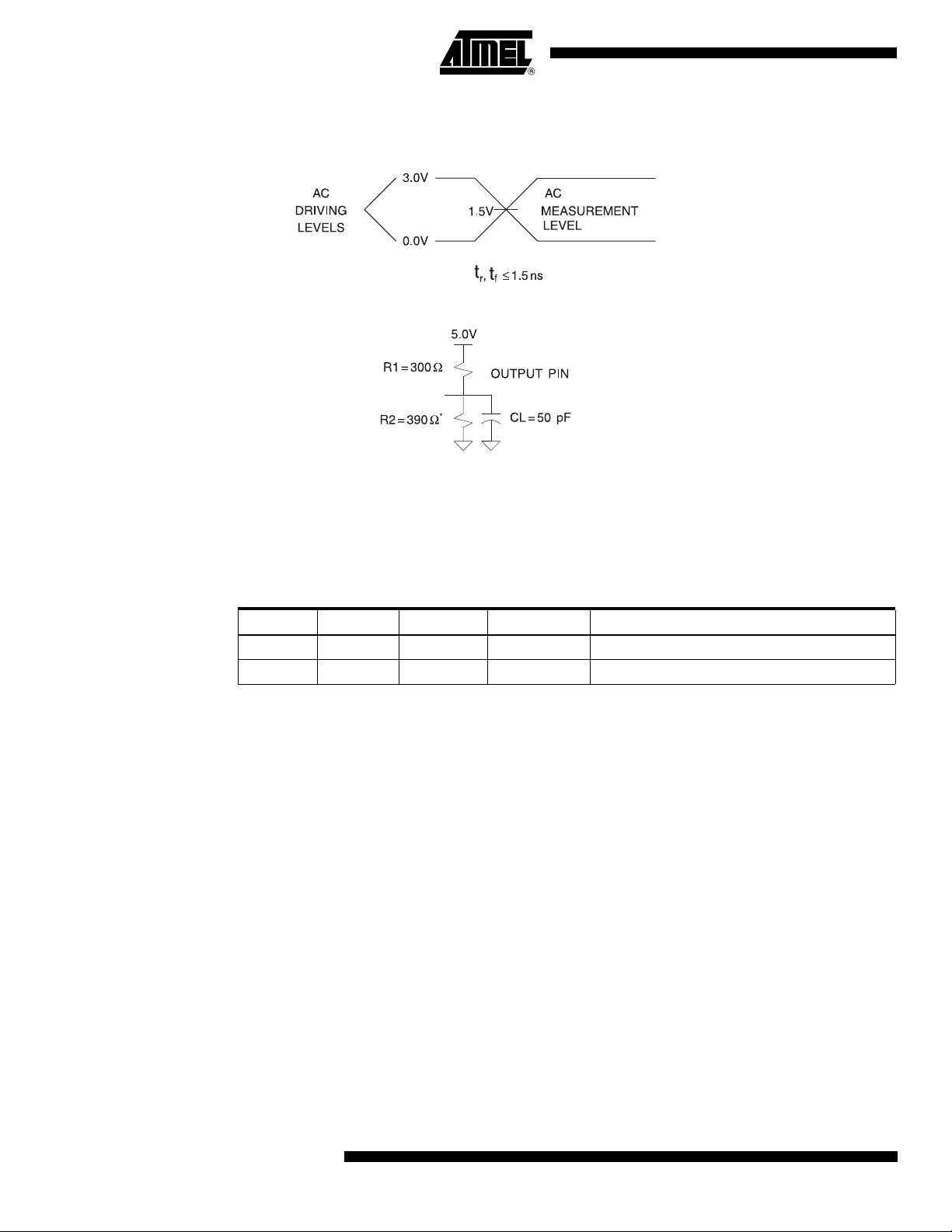
4.4 Input Test Waveforms
4.4.1 Input Test Waveforms and Measurement Levels
4.4.2 Output Test Loads
Note: Similar competitors devices are specified with slightly different loads. These load differences may
affect output signals’ delay and slew rate. Atmel devices are tested with sufficient margins to meet
compatible device specification conditions.
4.5 Pin Capacitance
Table 4-1. Pin Capacitance (f = 1 MHz, T = 25C
Typ Max Units Conditions
C
IN
C
I/O
Note: 1. Typical values for nominal supply voltage. This parameter is only sampled and is not 100%
tested.
4.6 Power-up Reset
The registers in the ATF22V10CZ/CQZ are designed to reset during power-up. At a point
delayed slightly from V
state will depend on the polarity of the buffer.
This feature is critical for state machine initialization. However, due to the asynchronous nature
of reset and the uncertainty of how V
required:
1. The V
rise must be monotonic and start below 0.7V.
CC
2. The clock must remain stable during T
3. After T
occurs, all input and feedback setup times must be met before driving the
PR
clock pin high.
4.7 Preload of Register Outputs
The ATF22V10CZ/CQZ’s registers are provided with circuitry to allow loading of each register
with either a high or a low. This feature will simplify testing since any state can be forced into the
registers to control test sequencing. A JEDEC file with preload is generated when a source file
(1)
)
810 pF V
810 pF V
crossing V
CC
, all registers will be reset to the low state. The output
RST
actually rises in the system, the following conditions are
CC
.
PR
= 0V; f = 1.0 MHz
IN
= 0V; f = 1.0 MHz
OUT
6
ATF22V10C(Q)Z
0778J–PLD–11/07

with vectors is compiled. Once downloaded, the JEDEC file preload sequence will be done auto-
C
LOCK
V
RST
POWER
REGISTERED
OUTPUTS
t
S
t
PR
t
W
matically by most of the approved programmers after the programming.
5. Electronic Signature Word
There are 64 bits of programmable memory that are always available to the user, even if the
device is secured. These bits can be used for user-specific data.
6. Security Fuse Usage
A single fuse is provided to prevent unauthorized copying of the ATF22V10CZ/CQZ fuse patterns. Once programmed, fuse verify and preload are inhibited. However, the 64-bit User
Signature remains accessible. The security fuse should be programmed last, as its effect is
immediate.
7. Programming/Erasing
Programming/erasing is performed using standard PLD programmers. See CMOS PLD Programming Hardware & Software Support for information on software/programming.
Figure 7-1. Programming/Erasing Timing
ATF22V10C(Q)Z
8. Input and I/O Pull-ups
0778J–PLD–11/07
Table 7-1. Programming/Erasing
Parameter Description Typ Max Units
T
PR
V
RST
Power-up
Reset Time
Power-up
Reset Voltage
600 1000 ns
3.8 4.5 V
All ATF22V10CZ/CQZ family members have internal input and I/O pin-keeper circuits. Therefore, whenever inputs or I/Os are not being driven externally, they will maintain their last driven
state. This ensures that all logic array inputs and device outputs are at known states. These are
relatively weak active circuits that can be easily overridden by TTL-compatible drivers (see input
and I/O diagrams below).
7

Figure 8-1. Input Diagram
100K
V
CC
ESD
PROTECTION
CIRCUIT
INPUT
100K
V
CC
V
CC
DATA
OE
I/O
INPUT
Figure 8-2. I/O Diagram
9. Compiler Mode Selection
Table 9-1. Compiler Mode Selection
Synario
WINCUPL
8
ATF22V10C(Q)Z
PAL M o de
(5828 Fuses)
ATF22V10C (DIP)
ATF22V10C (PLCC)
P22V10
P22V10LCC
GAL Mode
(5892 Fuses)
ATF22V10C DIP (UES)
ATF22V10C PLCC (UES)
G22V10
G22V10LCC
0778J–PLD–11/07

10. Functional Logic Diagram Description
The Functional Logic Diagram describes the ATF22V10CZ/CQZ architecture.
The ATF22V10CZ/CQZ has 12 inputs and 10 I/O macrocells. Each macrocell can be configured
into one of four output configurations: active high/low, registered/combinatorial output.The universal architecture of the ATF22V10CZ/CQZ can be programmed to emulate most 24-pin PAL
devices.
Unused product terms are automatically disabled by the compiler to decrease power consumption. A security fuse, when programmed, protects the contents of the ATF22V10CZ/CQZ. Eight
bytes (64 fuses) of User Signature are accessible to the user for purposes such as storing
project name, part number, revision or date. The User Signature is accessible regardless of the
state of the security fuse.
ATF22V10C(Q)Z
0778J–PLD–11/07
9

Figure 10-1. Functional Logic Diagram
10
ATF22V10C(Q)Z
0778J–PLD–11/07

ATF22V10CZ/CQZ STAND-BY ICC vs.
SUPPLY VOLTAGE (T
A
= 25°C)
0.0
0.5
1.0
1.5
2.0
2.5
3.0
3.5
4.0
4.5
4.5 4.8 5.0 5. 3 5.5
SUPPLY VOLTAGE (V)
ICC (µA)
NORMALIZED ICC VS. TEMP
0.4
0.6
0.8
1.0
1.2
1.4
-40.0 0.0 25.0 75.0
TEM PE RATURE (C)
NORMALI ZED I CC
ATF22V10CZ SUPPLY CURRENT vs. INPUT
FREQUENCY (VCC = 5.0V, TA = 25°C)
0.000
20.000
40.000
60.000
80.000
100.000
120.000
140.000
0.0 0.5 2.5 5.0 7.5 10. 0 25.0 37. 5 50.0
FREQ UENCY (MHz)
I
CC
(mA)
ATF22V10CQZ SUPPLY CURRENT VS.
INPUT FREQUENCY (V
CC
= 5V, TA = 25°C)
0.000
10.000
20.000
30.000
40.000
50.000
0.0 0.5 2. 5 5.0 7.5 10.0 25.0 37.5 50.0
FREQUENCY (MHz)
I
CC
(mA)
ATF22V10CZ/CQZ OUTPUT SOURCE CURRENT VS
SUPPLY VOLTAGE (V
OH
= 2.4V)
-50
-40
-30
-20
-10
0
4.0 4.5 5.0 5.5 6.0
SUPPLY VO LT AGE (V)
I
OH
(mA)
VS.
OUTPUT VOLTAGE (V
CC
= 5V, TA = 25°C)
-90.0
-80.0
-70.0
-60.0
-50.0
-40.0
-30.0
-20.0
-10.0
0.0
0.00 0.50 1.00 1.50 2.00 2.50 3.00 3.50 4.00 4.50 5.00
V
OH
(V)
I
OH
(mA)
ATF22V10CZ/CQZ OUTPUT SINK CURRENT vs.
SUPPLY VOLTAGE (V
OL
= 0.5V)
36
38
40
42
44
46
48
4.0 4.5 5.0 5.5 6.0
SUPPLY VOLTAGE (V)
I
OL
(mA)
ATF22V10CZ/CQZ OUTPUT SINK CURRENT VS.
SUPPLY VOLTAGE (V
OL
= 0.5V)
0.0
20.0
40.0
60.0
80.0
100.0
120.0
140.0
0.0 0.5 1.0 1.5 2.0 2.5 3.0 3.5 4.0 4.5 5.0
SUPPLY VOLTAGE (V)
I
OL
(mA)
ATF22V10C(Q)Z
0778J–PLD–11/07
ATF22V10CZ/CQZ OUTPUT SOURCE CURRENT
11

ATF22V10CZ/CQZ INPUT CLAMP CURRENT VS
INPUT VOLTAGE (V
CC
= 5V, TA = 35°C)
-120
-100
-80
-60
-40
-20
0
0.0 -0.2 -0.4 -0.6 -0.8 -1.0
INPUT VOLTAGE (V)
INP UT CURRE NT (m A)
ATF22V10CZ/CQZ INPUT CURRENT VS
INPUT VOLTAGE (V
CC
= 5V, TA = 25°C)
-30
-20
-10
0
10
20
30
40
0.0 1.0 2.0 3.0 4.0 5.0 6.0
INPUT VOLTAGE (V)
INPUT CURRENT (uA)
NORMALIZED TPD vs. VCC
0.8
0.9
1.0
1.1
1.2
4.5 4.8 5.0 5.3 5.5
SUPPLY VOLTAGE (V)
NORMALI ZED TPD
NORMALIZED TPD vs. TEMP
0.8
0.9
1.0
1.1
-40.0 0.0 25.0 75.0
TEM PE RATURE (C)
NORMALI ZE D TPD
NORMALIZED TCO vs. VCC
0.8
0.9
1.0
1.1
1.2
1.3
4.5 4. 8 5. 0 5. 3 5.5
SUPPLY VOLTAGE (V)
NORMALI ZED TCO
NORMALIZED TCO VS TEMP
0.8
0.9
1.0
1.1
-40.0 0.0 25.0 75.0
TEM PE RATURE (V )
NORMALI ZED T CO
NORMALIZED TSU VS VCC
0.8
0.9
1.0
1.1
1.2
4.5 4. 8 5.0 5.3 5.5
SUPPLY VOLTAGE (V)
NORMALI ZED TSU
NORMALIZED TSU vs. TEMP
0.8
0.9
1.0
1.1
1.2
-40.0 0.0 25.0 75.0
TEM PE RATURE (C)
NORMALI ZED TSU
12
ATF22V10C(Q)Z
0778J–PLD–11/07

ATF22V10C(Q)Z
ATF22V10C DELTA T
PD
OUTPUT LOADING
-2
0
2
4
6
8
0 50 100 150 200 250 300
OUTPUT LOADI NG (P F)
DELTA TPD (ns)
ATF22V10C DELTA T
CO
OUTPUT LOADING
0.00
1.00
2.00
3.00
4.00
5.00
6.00
7.00
8.00
50 100 150 200 250 300
NUMBER OF OUTP UTS LOADING
DELTA TCO (ns)
DELTA TPD vs. # OF OUTPUT SWITCHING
-0.5
-0.4
-0.3
-0.2
-0.1
0.0
1.02.03.04.05.06.07.08.09.010.0
NUMBER O F OUTP UTS SWITCHING
DELTA TPD (ns)
DELTA TCO vs. # OF OUTPUT SWITCHING
-0.3
-0.2
-0.2
-0.1
-0.1
0.0
1.0 2.0 3.0 4.0 5.0 6.0 7. 0 8.0 9. 0 10.0
NUMBER O F OUTP UTS SWITCHING
DELTA TCO (ns)
vs.
VS.
0778J–PLD–11/07
13

11. Ordering Information
11.1 Standard Package Options
t
PD
(ns)
12 10 8
15 4.5 8
20 14 12
t
S
(ns)
t
CO
(ns) Ordering Code Package Operation Range
ATF22V10CZ-12JC
ATF22V10CZ-12PC
ATF22V10CZ-12SC
ATF22V10CZ-12XC
ATF22V10CZ-15JC
ATF22V10CZ-15PC
ATF22V10CZ-15SC
ATF22V10CZ-15XC
ATF22V10CZ-15JI
ATF22V10CZ-15PI
ATF22V10CZ-15SI
ATF22V10CZ-15XI
ATF22V10CQZ-20JC
ATF22V10CQZ-20PC
ATF22V10CQZ-20SC
ATF22V10CQZ-20XC
ATF22V10CQZ-20JI
ATF22V10CQZ-20PI
ATF22V10CQZ-20SI
ATF22V10CQZ-20XI
28J
24P3
24S
24X
28J
24P3
24S
24X
28J
24P3
24S
24X
28J
24P3
24S
24X
28J
24P3
24S
24X
Commercial
(0°C to 70°C)
Commercial
(0°C to 70°C)
Industrial
(-40°C to +85°C)
Commercial
(0°C to 70°C)
Industrial
(-40°C to +85°C)
11.2 ATF22V10CQZ Green Package Options (Pb/Halide-free/RoHS Compliant)
t
PD
(ns)
20 14 12
t
S
(ns)
t
CO
(ns) Ordering Code Package Operation Range
ATF22V10CQZ-20JU
ATF22V10CQZ-20PU
ATF22V10CQZ-20SU
ATF22V10CQZ-20XU
28J
24P3
24S
24X
11.3 Using “C” Product for Industrial
To use commercial product for Industrial temperature ranges, down-grade one speed grade
from the “I” to the “C” device (7 ns “C” = 10 ns “I”) and de-rate power by 30%.
Package Type
28J 28-lead, Plastic J-leaded Chip Carrier (PLCC)
24P3 24-pin, 0.300", Plastic Dual Inline Package (PDIP)
24S 24-lead, 0.300" Wide, Plastic Gull-Wing Small Outline (SOIC)
24X 24-lead, 4.4 mm Wide, Plastic Thin Shrink Small Outline (TSSOP)
Industrial
(-40°C to +85°C)
14
ATF22V10C(Q)Z
0778J–PLD–11/07

12. Packaging Information
2325 Orchard Parkway
San Jose, CA 95131
R
TITLE
DRAWING NO.
REV.
B
28J, 28-lead, Plastic J-leaded Chip Carrier (PLCC)
28J
10/04/01
1.14(0.045) X 45˚
PIN NO. 1
IDENTIFIER
1.14(0.045) X 45˚
0.51(0.020)MAX
0.318(0.0125)
0.191(0.0075)
A2
45˚ MAX (3X)
A
A1
B1
D2/E2
B
e
E1 E
D1
D
COMMON DIMENSIONS
(Unit of Measure = mm)
SYMBOL
MIN
NOM
MAX
NOTE
Notes: 1. This package conforms to JEDEC reference MS-018, Variation AB.
2. Dimensions D1 and E1 do not include mold protrusion.
Allowable protrusion is .010"(0.254 mm) per side. Dimension D1
and E1 include mold mismatch and are measured at the extreme
material condition at the upper or lower parting line.
3. Lead coplanarity is 0.004" (0.102 mm) maximum.
A 4.191 – 4.572
A1 2.286 – 3.048
A2 0.508 – –
D 12.319 – 12.573
D1 11.430 – 11.582 Note 2
E 12.319 – 12.573
E1 11.430 – 11.582 Note 2
D2/E2 9.906 – 10.922
B 0.660 – 0.813
B1 0.330 – 0.533
e 1.270 TYP
12.1 28J – PLCC
ATF22V10C(Q)Z
0778J–PLD–11/07
15

12.2 24P3 – PDIP
2325 Orchard Parkway
San Jose, CA 95131
TITLE
DRAWING NO.
R
REV.
24P3, 24-lead (0.300"/7.62 mm Wide) Plastic Dual
Inline Package (PDIP)
D
24P3
6/1/04
PIN
1
E1
A1
B
E
B1
C
L
SEATING PLANE
A
D
e
eB
eC
COMMON DIMENSIONS
(Unit of Measure = mm)
SYMBOL
MIN
NOM
MAX
NOTE
A – – 5.334
A1 0.381 – –
D 31.623 – 32.131 Note 2
E 7.620 – 8.255
E1 6.096 – 7.112 Note 2
B 0.356 – 0.559
B1 1.270 – 1.651
L 2.921 – 3.810
C 0.203 – 0.356
eB – – 10.922
eC 0.000 – 1.524
e 2.540 TYP
Notes: 1. This package conforms to JEDEC reference MS-001, Variation AF.
2. Dimensions D and E1 do not include mold Flash or Protrusion.
Mold Flash or Protrusion shall not exceed 0.25 mm (0.010").
16
ATF22V10C(Q)Z
0778J–PLD–11/07

12.3 24S – SOIC
0º ~ 8º
PIN 1 ID
PIN 1
06/17/2002
2325 Orchard Parkway
San Jose, CA 95131
TITLE
DRAWING NO.
REV.
24S, 24-lead (0.300" body) Plastic Gull Wing Small Outline (SOIC)
B
24S
R
COMMON DIMENSIONS
(Unit of Measure = mm)
SYMBOL
MIN
NOM
MAX
NOTE
A – – 2.65
A1 0.10 – 0.30
D 10.00 – 10.65
D1 7.40 – 7.60
E 15.20 – 15.60
B 0.33 – 0.51
L 0.40 – 1.27
L1 0.23 – 0.32
e 1.27 BSC
B
D
D1
e
E
A
A1
L1
L
ATF22V10C(Q)Z
0778J–PLD–11/07
17

12.4 24X – TSSOP
0.30(0.012)
0.19(0.007)
4.48(0.176)
4.30(0.169)
6.50(0.256)
6.25(0.246)
0.65(0.0256)BSC
7.90(0.311)
7.70(0.303)
0.15(0.006)
0.05(0.002)
0.20(0.008)
0.09(0.004)
0.75(0.030)
0.45(0.018)
0º ~ 8º
1.20(0.047)MAX
Dimensions in Millimeter and (Inches)*
JEDEC STANDARD MO-153 AD
Controlling dimension: millimeters
PIN 1
04/11/2001
2325 Orchard Parkway
San Jose, CA 95131
TITLE
DRAWING NO.
R
REV.
24X, 24-lead (4.4 mm body width) Plastic Thin Shrink Small Outline
Package (TSSOP)
A
24X
18
ATF22V10C(Q)Z
0778J–PLD–11/07

13. Revision History
Version No./Release Date History
Revision I – November 2005
1. Added Green Package options
ATF22V10C(Q)Z
0778J–PLD–11/07
19

Headquarters International
Atmel Corporation
2325 Orchard Parkway
San Jose, CA 95131
USA
Tel: 1(408) 441-0311
Fax: 1(408) 487-2600
Atmel Asia
Room 1219
Chinachem Golden Plaza
77 Mody Road Tsimshatsui
East Kowloon
Hong Kong
Tel: (852) 2721-9778
Fax: (852) 2722-1369
Product Contact
Web Site
www.atmel.com
Literature Requests
www.atmel.com/literature
Atmel Europe
Le Krebs
8, Rue Jean-Pierre Timbaud
BP 309
78054 Saint-Quentin-enYvelines Cedex
France
Tel: (33) 1-30-60-70-00
Fax: (33) 1-30-60-71-11
Technical Support
pld@atmel.com
Atmel Japan
9F, Tonetsu Shinkawa Bldg.
1-24-8 Shinkawa
Chuo-ku, Tokyo 104-0033
Japan
Tel: (81) 3-3523-3551
Fax: (81) 3-3523-7581
Sales Contact
www.atmel.com/contacts
Disclaimer: The information in this document is provided in connection with Atmel products. No license, express or implied, by estoppel or otherwise, to any
intellectual property right is granted by this document or in connection with the sale of Atmel products. EXCEPT AS SET FORTH IN ATMEL’S TERMS AND CONDI-
TIONS OF SALE LOCATED ON ATMEL’S WEB SITE, ATMEL ASSUMES NO LIABILITY WHATSOEVER AND DISCLAIMS ANY EXPRESS, IMPLIED OR STATUTORY
WARRANTY RELATING TO ITS PRODUCTS INCLUDING, BUT NOT LIMITED TO, THE IMPLIED WARRANTY OF MERCHANTABILITY, FITNESS FOR A PARTICULAR
PURPOSE, OR NON-INFRINGEMENT. IN NO EVENT SHALL ATMEL BE LIABLE FOR ANY DIRECT, INDIRECT, CONSEQUENTIAL, PUNITIVE, SPECIAL OR INCIDENTAL DAMAGES (INCLUDING, WITHOUT LIMITATION, DAMAGES FOR LOSS OF PROFITS, BUSINESS INTERRUPTION, OR LOSS OF INFORMATION) ARISING OUT OF
THE USE OR INABILITY TO USE THIS DOCUMENT, EVEN IF ATMEL HAS BEEN ADVISED OF THE POSSIBILITY OF SUCH DAMAGES. Atmel makes no
representations or warranties with respect to the accuracy or completeness of the contents of this document and reserves the right to make changes to specifications
and product descriptions at any time without notice. Atmel does not make any commitment to update the information contained herein. Unless specifically provided
otherwise, Atmel products are not suitable for, and shall not be used in, automotive applications. Atmel’s products are not intended, authorized, or warranted for use
as components in applications intended to support or sustain life.
© 2007 Atmel Corporation. All rights reserved. Atmel®, logo and combinations thereof, Everywhere You Are® and others, are registered trade-
marks or trademarks of Atmel Corporation or its subsidiaries. Other terms and product names may be trademarks of others.
0778J–PLD–11/07
 Loading...