

ATMEL ATF22LV10CZ-25XI, ATF22LV10CZ-25XC, ATF22LV10CZ-25SI, ATF22LV10CZ-25SC, ATF22LV10CZ-25PI Datasheet
...
Features
3.0V to 5.5V Operating Ra ng e
•
Advanced Low Voltage, Zero Power,
•
Electrically Erasable Programmable Logic Device
Edge-Sensing “Zero” Power
•
Low Voltage Equivalent of ATF22V10CZ
•
“Zero” Standby Power (25 µA Maximum)
•
Ideal for Battery Powered Systems
•
25 ns Maximum Propag ation Delay
•
CMOS and TTL Compatible Inputs and Outputs
•
Latch Feature Hold Inputs to Previous Logic States
•
Advanced E2 Technology
•
Reprogrammable
100% Tested
High Reliability CMOS Process
•
20 Year Data Retention
100 Erase/Write Cyc le s
2,000V ESD Protection
200 mA Latchup Immunity
Commercial and Industrial Temperature Ranges
•
Dual-in-Line and Surface Mount Standard Pinouts
•
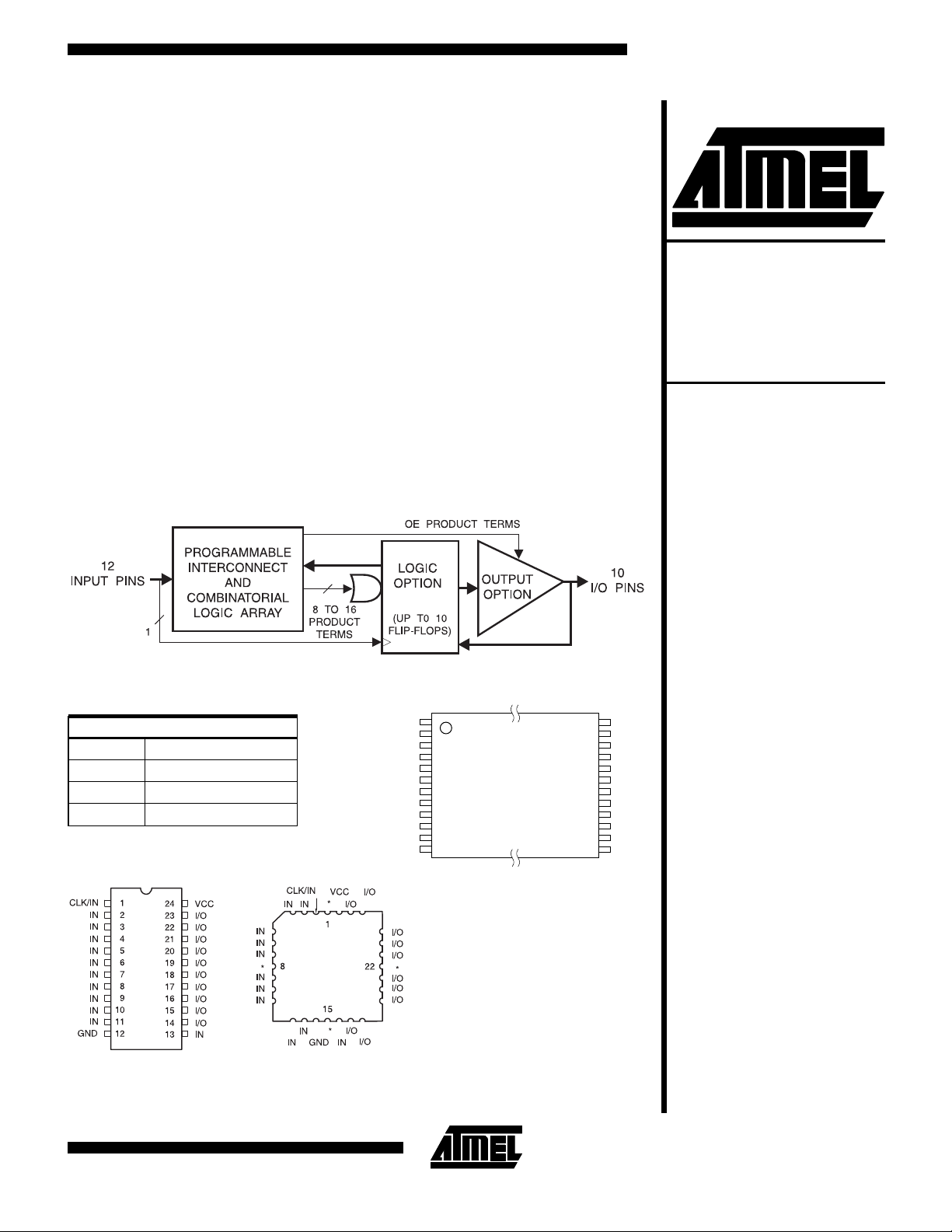
Block Diagram
High
Performance
2
E
PLD
ATF22LV10CZ
Pin Configurations
Pin Name Function
CLK Clock
IN Logic Inputs
I/O Bidirectional Buffers
V
CC
(3 to 5.5V) Supply
DIP/SOIC
CLK/IN
GND
PLCC
TSSOP Top View
1
2
IN
3
IN
4
IN
5
IN
6
IN
7
IN
8
IN
9
IN
10
IN
11
IN
12
Top view
Note: For PLCC, pi ns 1 , 8, 15, and 22 ca n be l ef t unconnected. Fo r s up erior performance, connect V
to pin 1 and GND to pins 8, 15 , an d 22 .
CC
ATF22LV10CZ
24
VCC
23
I/O
22
I/O
21
I/O
20
I/O
19
I/O
18
I/O
17
I/O
16
I/O
15
I/O
14
I/O
13
IN
Rev. 0779E/LV10CZ-E–05/98
Description
The ATF22LV10CZ is a high performance CMOS (Electrically Erasable) Programmable Logic Device (PLD) which
utilizes Atmel’s proven electrically erasable Flash memory technology and provides 25 ns speed with stand-by
current of 25 µA maximum. All speed ranges are specified
over the 3.0V to 5.5V range for industrial and commercial
temperature ranges.
The ATF22LV10CZ provides a low voltage and edgesensing “zero” power CMOS PLD solution with “zero”
standby power (5 µA typical). The ATF22LV10CZ powers
down automatically to the zero power mode through Atmel’s patented Input Transition Detection (ITD) circuitry
when the device is idle. The ATF22LV10CZ is capable of
Absolute Maximum Ratings*
operating at supply voltages down to 3.0V. Pin “keeper”
circuits on input and output pins hold pins to their previous
logic levels when idle, which eliminate static power consumed by pull-up resistors.
The ATF22LV10CZ mac rocell incorporates a variable
product term architecture. Each output is allocated from 8
to 16 product terms whic h allows highly complex logic
functions to be realized. Two additional product terms are
included to provide synchronous reset and asynchronous
reset. These additional product terms are common to all
10 registers and are automatically cleared upon power up.
Register Preload simplifies testing. A Security Fuse prevents unauthorized copying of programmed fuse patterns.
Temperature Under Bias...................-40°C to +85°C
Storage Temperature......................-65°C to +150°C
Voltage on Any Pin with
Respect to Ground.........................-2.0V to +7.0V
Voltage on Input Pins
with Respect to Ground
During Programming....................-2.0V to +14.0V
Programming Voltage with
Respect to Ground.......................-2.0V to +14.0V
(1)
(1)
(1)
*NOTICE: Stresses beyond those listed under “ Absolute Maxi-
mum Ratings” may cause permanent damage to the device.
This is a stress rating only and functional operation of the
device at these or an y ot he r con ditions beyond tho se ind icated in the oper ational sections of this specification is not
implied. Exposure to absolute maximum rating conditions
for extended periods may affect device reliability.
Note: 1. Minimum voltage is -0.6V dc, which may undershoot
to -2.0V for pulses of less than 20 ns. Maximum output pin voltage is Vcc + 0.75V dc, which may overshoot to 7.0V for pulses of less than 20 ns.
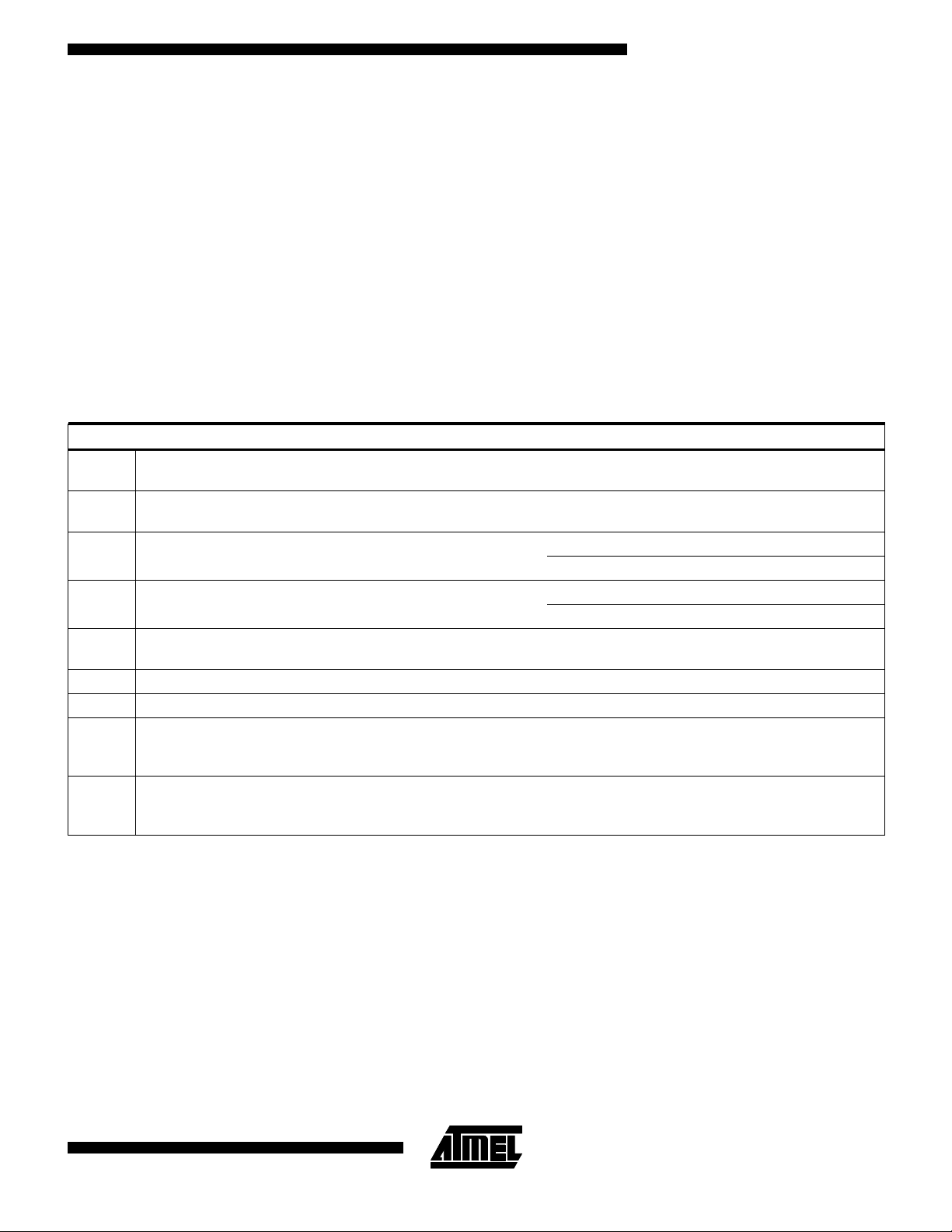
DC and AC Operating Conditions
Commercial Industrial
Operating Temperature (Case) 0°C - 70°C -40°C - 85°C
V
Power Supply 3.0V - 5.5V 3.0V - 5.5V
CC
2
ATF22LV10CZ
ATF22LV10CZ
Functional Logic Diagram Description
The Functional Logic Diagram describes the
ATF22LV10CZ architecture.
The ATF22LV10CZ has 12 inputs and 10 I/O macrocells.
Each macrocell can be configured into one of four output
configurations: active-high/low or registered/combinatorial. The universal architecture of the ATF22LV10CZ can
be programmed to emulate most 24-pin PAL devices.
DC Characteristics
Symbol Parameter Condition Min Typ Max Units
I
I
I
I
I
V
V
V
V
IL
IH
CC
SB
OS
IL
IH
OL
OH
Input or I/O Low
Leakage Current
Input or I/O High
Leakage Current
Clocked Power
Supply Current
Power Supply Current,
Standby
Output Short Circuit
(1)
Current
0 ≤ V
V
≤ VIL(MAX) -10 µA
IN
- 0.7V ≤ VIN ≤ V
CC
VCC = MAX,
Outputs Open, f = 15 MHz
VCC = MAX,
V
= MAX, Outputs Open
IN
V
= 0.5V -130 mA
OUT
Input Low Voltage -0.5 0.8 V
Input High Voltage 2.0 VCC + 0.75 V
= VIH or V
V
Output Low Voltage
Output High Voltage
IN
VCC = MIN,
I
= 8 mA
OL
= VIH or VIL,
V
IN
V
= MIN,
CC
I
= -4.0 mA
OH
IL
Unused product terms are automatically disabled by the
compiler to decrease power consumption. A Security
Fuse, when programmed, protects the contents of the
ATF22LV10CZ. Eight bytes (64 fuses) of User S ignature
are accessible to the user for purposes such as storing
project nam e, part number, revision or date. The User
Signature is accessible regardless of the state of the Security Fuse.
CC
10 µA
Com. 55 85 mA
Ind. 60 90 mA
Com. 5 25 µA
Ind. 5 50 µA
Com.
0.5 V
Ind.
2.4 V
Note: 1. Not more than one output at a time should be shorted. Duration of short circuit test should not exceed 30 sec.
3
 Loading...