

Datasheet ATF16V8C-7PC, ATF16V8C-7JI, ATF16V8C-7JC, ATF16V8C-5JC, ATF16V8C-7XI Datasheet (ATMEL)
...Page 1
Features
Industry Standard Architecture
•
Emulates Many 20-Pin PALs
Low Cost Easy-to-Use Software Tools
High Speed Electrically Erasable Programmable Logic Devices
•
5 ns Maximum Pin-to-Pin Delay
Low Power - 100 µA Pin-Controlled Power Down Mode Option
•
CMOS and TTL Compatible Inputs and Outputs
•
I/O Pin Keeper Circuits
Advanced Flash Tech no lo gy
•
Reprogrammable
100% Tested
High Reliability CMOS Process
•
20 Year Data Retention
100 Erase/Write Cyc le s
2,000V ESD Protection
200 mA Latchup Immunity
Commercial and Industrial Temperature Ranges
•
Dual-in-Line and Surface Mount Packages in Standard Pinouts
•
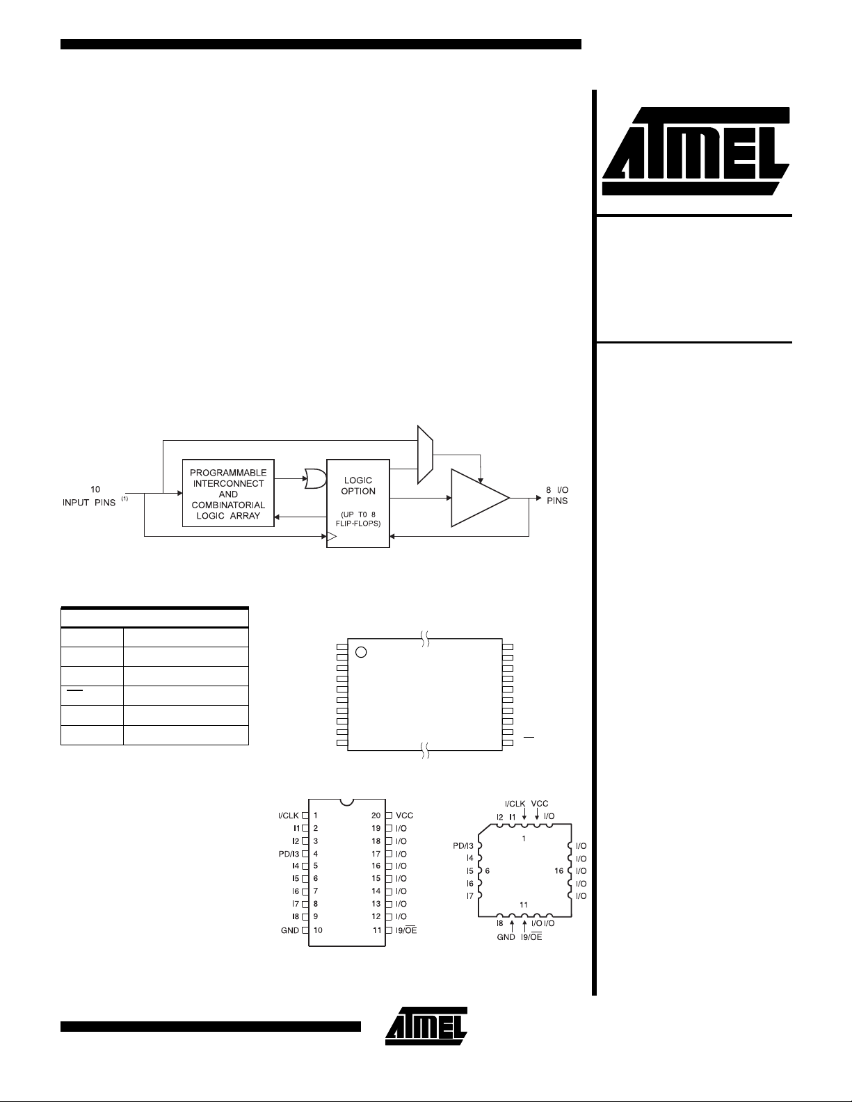
Block Diagram
High
Performance
2
E
PLD
ATF16V8C
Note: 1. Includes optional PD control pin.
Pin Configurations
Pin Name Function
CLK Clock
I Logic Inputs
I/O Bidirectional Buffers
OE Output Enable
VCC +5V Supply
PD Power Down
TSSOP Top View
1
I/CLK
PD/I3
GND
2
I1
3
I2
4
5
I4
6
I5
7
I6
8
I7
9
I8
10
20
VCC
19
I/O
18
I/O
17
I/O
16
I/O
15
I/O
14
I/O
13
I/O
12
I/O
11
I9/OE
DIP/SOIC PLCC
Top view
ATF16V8C
Rev. 0425D/V16FC-D–04/98
Page 2
Description
The ATF16V8C is a high performance EECMOS Programmable Logic Device that utilizes Atmel’s proven electrically erasable Flash memory technology. S peeds down
to 5 ns and a 100 µA pin-controlled power down mode option are offered. All speed ranges are specified over the
full 5V ± 10% range for industrial temperature ranges; 5V
± 5% for commercial range 5-volt devices.
The ATF16V8C incorporates a superset of the generic architectures, which allows direct replacement of the 16R8
family and most 20-pin combinatorial PLDs. Eight outputs
are each allocated eight product terms. Three different
Absolute Maximum Ratings*
Temperature Under Bias...................-40°C to +85°C
Storage Temperature......................-65°C to +150°C
Voltage on Any Pin with
Respect to Ground.........................-2.0V to +7.0V
Voltage on Input Pins
with Respect to Ground
During Programming....................-2.0V to +14.0V
Programming Voltage with
Respect to Ground.......................-2.0V to +14.0V
(1)
(1)
(1)
modes of operation, configured automatically with software, allow highly complex logic functions to be realized.
The ATF16V8C can significantly reduce total system
power, thereby enhancing system reliability and reducing
power supply costs. When pin 4 is configured as the
power down control pin , supply current drops to less than
100 µA whenever the pin is high. If the power down feature isn’t required for a particular application, pin 4 may be
used as a logic input. Also, the pin keeper circuits eliminate the need for internal pull-up resistors along with their
attendant power consumption.
*NOTICE: Stresses beyond those listed under “Absolute Maxi-
mum Ratings” may cause permanent damage to the device.
This is a stress rating only and functional operation of the
device at these or an y ot he r con ditions beyond those indicated in the oper ational sections of this specification is not
implied. Exposure to absolute maximum rating conditions
for extended periods may affect device reliability.
Note:
1. Minimum voltage is -0.6V dc, which may undershoot to -
2.0V for pulses of less than 20 ns. Maximum output pin
voltage is Vcc + 0.75 V dc, whic h may overshoot to 7. 0V
for pulses of le ss than 20 ns.
DC and AC Operating Conditions
Commercial Industrial
Operating Temperature (Case) 0°C - 70°C -40°C - 85°C
V
Power Supply 5V ± 5% 5V ± 10%
CC
2
ATF16V8C
Page 3
ATF16V8C
DC Characteristics
Symbol Parameter Condition Min Typ Max Units
I
IL
I
IH
I
CC1
I
PD
I
OS
V
IL
V
IH
V
OL
V
OH
I
OL
I
OH
Note: 1. All ICC parameters measure d wit h outputs open.
Input or I/O Low
Leakage Current
Input or I/O High
Leakage Current
Power Supply Current,
(1)
Standby
Power Supply Current,
Power Down Mode
Output Short Circuit
Current
0 ≤ V
3.5 ≤ V
15 MHz, V
V
≤ VIL(MAX) -10 µA
IN
≤ V
IN
CC
= 0, V
IN
CC,
Open
VCC = MAX,
V
= 0, V
V
V
IN
OUT
CC
CC
= 0.5V;
= 5V; TA = 25°C
CC
= MAX,
Outputs
10 µA
Com. 115 mA
Ind. 130 mA
Com. 10 100 µA
Ind. 10 105 µA
-150 mA
Input Low Voltage MIN < VCC < MAX -0.5 0.8 V
Input High Voltage 2.0 VCC + 1 V
= MIN; All Outputs
V
Output Low Voltage
Output High Voltage
Output Low Current VCC = MIN
CC
I
= 24 mA
OL
= MIN
V
CC
I
= -4.0 mA
OL
Com., Ind. 0.5 V
2.4 V
Com. 24 mA
Ind. 12 mA
Output High Current VCC = MIN Com., Ind. -4 mA
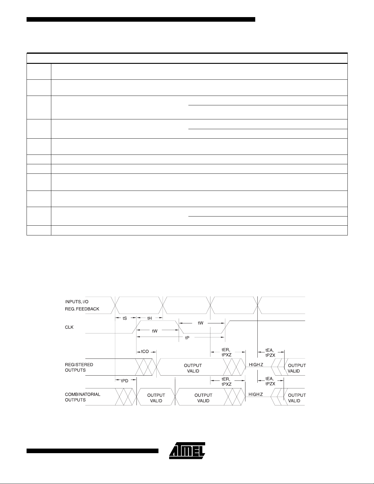
AC Waveforms
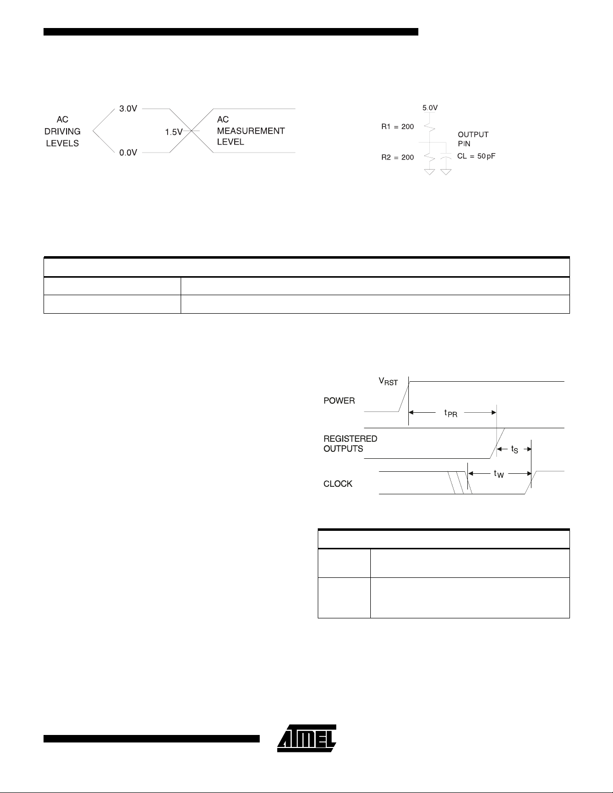
Note: 1. Timing measuremen t reference is 1.5V. In pu t AC driv in g le ve ls ar e 0. 0V an d 3.0V, unless otherw is e sp ec ified.
(1)
3
Page 4
AC Characteristics
Symbol Parameter
t
PD
t
CF
t
CO
t
S
t
H
t
P
t
W
F
t
EA
t
ER
t
PZX
t
PXZ
Input or Feedback to Non-Registered
Output
Clock to Feedback 3 3 ns
Clock to Output 1425ns
Input or Feedback Setup Time 3 5 ns
Input Hold Time 0 0 ns
Clock Period 6 8 ns
Clock Width 3 4 ns
External Feedback 1/(tS+ tCO) 142 100 MHz
MAX
Internal Feedback 1/(t
No Feedback 1/(t
Input to Output Enable —
Product Term
Input to Output Disable —
Product Term
OE pin to Output Enable 2526ns
OE pin to Output Disable 1.5 5 1.5 6 ns
-5 -7
Min Max Min Max
Units
1537.5ns
+ tCF) 166 125 MHz
S
) 166 125 MHz
P
2639ns
2529ns
Power Down AC Characteristics
Symbol Parameter
t
IVDH
t
GVDH
t
CVDH
t
DHIX
t
DHGX
t
DHCX
t
DLIV
t
DLGV
t
DLCV
t
DLOV
Notes: 1. Output data is latched an d he ld .
Valid Input Before PD High 5 7.5 ns
Valid OE Before PD High 0 0 ns
Valid Clock Before PD High 0 0 ns
Input Don’t Care After PD High 5 7.5 ns
OE Don’t Care After PD High 5 7.5 ns
Clock Don’t Care After PD High 5 7.5 ns
PD Low to Valid Input 5 7.5 ns
PD Low to Valid OE 15 20 ns
PD Low to Valid Clock 15 20 ns
PD Low to Valid Output 20 25 ns
2. HI-Z outputs remain HI-Z.
(1, 2, 3)
-5 -7
Min Max Min Max
3. Clock and input transitions are ignored.
Units
4
ATF16V8C
Page 5
ATF16V8C
Input Test Waveforms and
Measurement Levels:
tR, tF < 1.5ns (10% to 90%)
Pin Capacitance
C
IN
C
OUT
Note: 1. Typical values for nominal supply voltage. This parameter is only sampled and is not 100% tested.
(f = 1 MHz, T = 25°C)
Typ Max Units Conditions
58pFV
68pFV
(1)
Output Test Loads:
Commercial
= 0V
IN
OUT
= 0V
Power Up Reset
The ATF16V8C’s registers are designed to reset during
power up. At a point delayed slightly from V
, all registers will be reset to the low state. As a result,
V
RST
the registered output state will always be high on powerup.
This feature is critical for state machine initialization. However, due to the asynchronous nature of reset and the uncertainty of how V
lowing conditions are required:
1) The V
2) After reset occurs, all input and feedback setup times
must be met before driving the clock term high, and
3) The signals from which the clock is derived must remain stable during t
rise must be monotonic, from below .7 volts,
CC
actually rises in the system, the fol-
CC
.
PR
crossing
CC
Parameter Description Typ Max Units
t
V
PR
RST
Power-Up
Reset Time
Power-Up
Reset
Voltage
600 1,000 ns
3.8 4.5 V
5
Page 6

Power Down Mode
The ATF16V8C includes an optional pin controlled power
down feature. Device pin 4 may be configured as the
power down pin. When this feature is enabled and the
power down pin is high, total current consumption drops to
less than 100 µA. In the power down mode, all output data
and internal logic states are latched and held. All registered and combinatorial output data remains valid. Any
outputs which were in a HI-Z state at the onset of power
down will remain at HI-Z. During power down, all input signals except the power down pin are blocked. The input
and I/O pin keeper circuits remain active to insure that
pins do not float to indeterminate levels. This helps to further reduce system power.
Selection of the power down option is specified in the
ATF16V8C logic design file. The logic compiler will include
this option selection in the otherwise standard 16V8
JEDEC fuse file. When the power down feature is not
specified in the design file, pin 4 is available as a logic
input, and there is no power down pin. This allows the
ATF16V8C to be programmed using any existing standard 16V8 fuse file.
Note: Some programmers list the JEDEC-compatible
16V8C (No PD used) separately from the non-JEDEC
compatible 16V8CEXT. (EXT for extended features.)
Registered Output Preload
The ATF16V8C’s registers are provided with circuitry to
allow loading of each register with either a high or a low.
This feature will simplify testing since any state can be
forced into the registers to control test sequencing. A
JEDEC file with preload is generated when a source file
with vectors is compiled. Once downloaded, the JEDEC
file preload sequence will be done automatically by approved programmers.
Input and I/O Pin Keeper Circuits
The ATF16V8C contains internal input and I/O pin keeper
circuits. These circuits allow each ATF16V8C pin to hold
its previous value even when it is not being driven by an
external source or by the device’s output buffer. This helps
insure that all logic array inputs are at known, valid logic
levels. This reduces system power by preventing pins
from floating to indeterminate levels. By using pin keeper
Input Diagram
Security Fuse Usage
A single fuse is provided to prevent unauthorized copying
of the ATF16V8C fuse patterns. Once programmed, fuse
verify and preload are inhibited. However, the 64-bit User
Signature remains accessible.
The security fuse will be programmed last, as its effect is
immediate.
circuits rather than pull-up resistors, there is no DC current
required to hold the pins in either logic state (high or low).
These pin keeper circuits are implemented as weak feedback inve rters, as shown in the Input Diagram below.
These keeper circuits can easily be overdriven by standard TTL- or CMOS-compatible drivers. The typical overdrive current required is 40 µA.
I/O Diagram
6
ATF16V8C
Page 7

Functional Logic Diagram Description
The Logic Option and Functional Diagrams describe the
ATF16V8C architecture. Eight configurable macrocells
can be configured as a registered output, combinatorial
I/O, combinatorial output, or dedicated input.
The ATF16V8C can be configured in one of three different
modes. Each mode makes the ATF16V8C look lik e a different device. Most PLD compilers can choose the right
mode automatically. The user can also force the selection
by supplying the compiler with a mode selection. The determining factors would be the usage of register versus
combinatorial outputs and dedicated outputs versus outputs with output enable control.
The ATF16V8C universal architecture can be programmed to emulate many 20-pin PAL devices. These ar-
Compiler Mode Selection
ATF16V8C
chitectural subsets can be found in each of the configuration modes described in the following pages. The user can
download the listed subset device JEDEC programming
file to the PLD programmer, and the ATF16V8C can be
configured to act like the chosen device. Check with your
programmer manufacturer for this capability.
Unused product terms are automatically disabled by the
compiler to decrease power cons umption. A Security
Fuse, when programmed, protects the content of the
ATF16V8C. Eight bytes (64 fuses) of User Signatur e are
accessible to the user for purposes such as storing project
name, part number, revision, or date. The User Signature
is accessible regardless of the state of the Security Fuse.
Registered Complex Simple Auto Select
ABEL, Atmel-ABEL
with PD ENABLE
CUPL, Atmel-CUPL
with PD ENABLE
LOG/iC
OrCAD-PLD
PLDesigner
Synario/Atmel-Synario
with PD ENABLE
Tango-PLD
Notes: 1. Please call Atmel PLD Hotline at (408) 436-4333 for more inf ormation.
2. Only applicable for version 3.4 or lower.
P16V8R P16V8C P16V8AS P16V8
P16V8PDR
G16V8MS G16V8MA G16V8AS G16V8A
G16V8CPMS G16V8CPMA G16V8CPAS G16V8CP
GAL16V8_R
“Registered” “Complex” “Simple” GAL16V8A
P16V8R P16V8C P16V8C P16V8A
NA NA NA ATF16V8C ALL
NA NA NA ATF16V8C (PD) ALL
G16V8R G16V8C G16V8AS G16V8
(1)
(2)
P16V8PDC
GAL16V8_C7
(1)
(2)
P16V8PD
GAL16V8_C8
(1)
(2)
P16V8PDS
GAL16V8
(1)
(1)
7
Page 8

Macrocell Configuration
Software compilers support the three different OMC
modes as different device types. These devic e types are
listed in the table below. Most compilers have the ability to
automatically select the device type, generally based on
the register usage and output enable (OE) usage. Register usage on the device forces the software to choose the
registered mode. All combinatorial outputs with OE controlled by the product term will force the software to
choose the complex mode. The software will choose the
simple mode only when all outputs are dedicated combinatorial without OE control. The different device types
listed in the table can be used to override the automatic
device selection by the software. For further details, refer
to the compiler software manuals.
When using compiler software to configure the device, the
user must pay special attention to the following restrictions
in each mode.
ATF16V8C Registered Mode
PAL Device Emulation / PAL Replacement
The registered mode is used if one or more registers are
required. Eac h macrocell can be configured as either a
registered or combinatorial output or I/O, or as an input.
For a registered output or I/O, the output is enabled by the
OE pin, and the register is clocked by the CLK pin. Eight
product terms are allocated to the sum term. For a combinatorial output or I/O, the output enable is controlled by a
product term, and seven product terms are allocated to the
In
registered mode
figured as clock and output enable, respectively. These
pins cannot be configured as dedicated inputs in the registered mode.
In
complex mode
puts and use the feedback paths of pin 19 and pin 12 respectively. Because of this feedback path usage, pin 19
and pin 12 do not have the feedback option in this mode.
In
simple mode
routed via the adjacent pins. In doing so, the two inner
most pins (pins 15 and 16) will not have the feedback option as these pins are always configured as dedicated
combinatorial output.
sum term. When the macrocell is configured as an input,
the output enable is permanently disabled.
Any regis ter usage will make the compiler select this
mode. The following registered devices can be emulated
using this mode:
16R8 16RP8
16R6 16RP6
16R4 16RP4
pin 1 and pin 11 are permanently con-
pin 1 and pin 11 become dedicated in-
all feedback paths of the output pins are
Registered Configuration
for Registered Mode
Notes:
1. Pin 1 controls common CLK for the registered outputs.
Pin 11 controls common OE for the registered outputs.
Pin 1 and Pin 11 are permanently configured as CLK and
2. The development software configures all the archi tecture
control bits and checks for proper pin usage automatically.
8
ATF16V8C
(1, 2)
OE.
Combinatorial Configuration for
Registered Mode
Notes:
1. Pin 1 and Pin 11 are permanently configured as CLK and
OE.
2. The development software configures all the archi tecture
control bits and checks for proper pin usage automatically.
(1, 2)
Page 9

Registered Mode Logic Diagram
*
ATF16V8C
* Input not available if power down mode is enabled.
9
Page 10

ATF16V8C Complex Mode
PAL Device Emulation/PAL Replacement
In the Complex Mode, combinatorial output and I/O func-
tions are possible. Pins 1 and 11 are regular inputs to the
array. Pins 13 through 18 have pin feedback paths back to
the AND-array, which makes full I/O capability possible.
Pins 12 and 19 (outermost macrocells) are outputs only.
They do not have input capability. In this mode, each
macrocell has seven product terms going to the sum term
and one product term enabling the output.
Complex Mode Option
Combinatorial applications with an OE requirement will
make the compiler select this mode. The following devices
can be emulated using this mode:
16L8
16H8
16P8
ATF16V8C Simple Mode
PAL Device Emulation / PAL Replacement
In the Simple Mode, 8 product terms are allocated to the
sum term. Pins 15 and 16 (center macrocells) are permanently configured as combinatorial outputs. Other macrocells can be either inputs or combinatorial outputs with pin
feedback to the AND-array. Pins 1 and 11 are regular inputs.
Simple Mode Option
0
7
XOR
Pins 15 and 16 do not have this feedback path.
The compiler selects this mode when all outputs are combinatorial without OE control. The following simple PALs
can be emulated using this mode:
10L8 10H8 10P8
12L6 12H6 12P6
14L4 14H4 14P4
16L2 16H2 16P2
V
CC
0
S1*
1
10
* - Pins 15 and 16 are always enabled.
ATF16V8C
Page 11

Complex Mode Logic Diagram
*
ATF16V8C
* Input not available if power down mode is enabled.
11
Page 12

Simple Mode Logic Diagram
*
* Input not available if power down mode is enabled.
12
ATF16V8C
Page 13

ATF16V8C
13
Page 14

14
ATF16V8C
Page 15

ATF16V8C
15
Page 16

Ordering Information
t
PD
(ns)
5 3 4 ATF16V8C-5JC 20J Commercial
7.5 5 5 ATF16V8C-7JC 20J Commercial
t
S
(ns)
t
CO
(ns)
Ordering Code Package Operation Range
(0°C to 70°C)
ATF16V8C-7PC 20P3 (0°C to 70°C)
ATF16V8C-7SC 20S
ATF16V8C-7XC 20X
ATF16V8C-7JI 20J Industrial
ATF16V8C-7PI 20P3 (-40°C to 85°C)
ATF16V8C-7SI 20S
ATF16V8C-7XI 20X
16
20J
20P3
20S
20X
Package Type
20-Lead, Plastic J-Leaded Chip Carrier (PLCC)
20-Lead, 0.300" Wide, Plastic Dual Inline Package (PDIP)
20-Lead, 0.300" Wid e, Plastic Gull Wing Smal l O ut li ne (SOIC )
20-Lead, 4.4 mm Wide, Plastic Thin Shrink Small Outline (TSSOP)
ATF16V8C
 Loading...