

Atmel ATF16V8B, ATF16V8BQL, ATF16V8BQ User Manual
Features
• Industry-standard Architecture
– Emulates Many 20-pin PALs
– Low-cost Easy-to-use Software Tools
• High-speed Electrically-erasable Programmable Logic Devices
– 10 ns Maximum Pin-to-pin Delay
• Several Power Saving Options
Device ICC, Standby ICC, Active
®
ATF16V8B 50 mA 55 mA
ATF16V8BQ 35 mA 40 mA
ATF16V8BQL 5 mA 20 mA
• CMOS and TTL Compatible Inputs and Outputs
– Input and I/O Pull-up Resistors
• Advanced Flash Technology
– Reprogrammable
– 100% Tested
• High-reliability CMOS Process
– 20 Year Data Retention
– 100 Erase/Write Cycles
– 2,000V ESD Protection
– 200 mA Latchup Immunity
• Commercial, and Industrial Temperature Ranges
• Dual-in-line and Surface Mount Packages in Standard Pinouts
• PCI-compliant
• Green Package Options (Pb/Halide-free/RoHS Compliant) Available
1. Description
The ATF16V8B is a high-performance CMOS (electricallyerasable) programmable
logic device (PLD) that utilizes Atmel’s proven electrically-erasable Flash memory
technology. All speed ranges are specified over the full 5V ± 10% range for industrial
temperature ranges, and 5V ± 5% for commercial temperature ranges.
Highperformance
EE PLD
ATF16V8B
ATF16V8BQ
ATF16V8BQL
Several low-power options allow selection of the best solution for various types of
power-limited applications. Each of these options significantly reduces total system
power and enhances system reliability.
The ATF16V8Bs incorporate a superset of the generic architectures, which allows
direct replacement of the 16R8 family and most 20-pin combinatorial PLDs. Eight outputs are each allocated eight product terms. Three different modes of operation,
configured automatically with software, allow highly complex logic functions to be
realized.
0364J–PLD–7/05
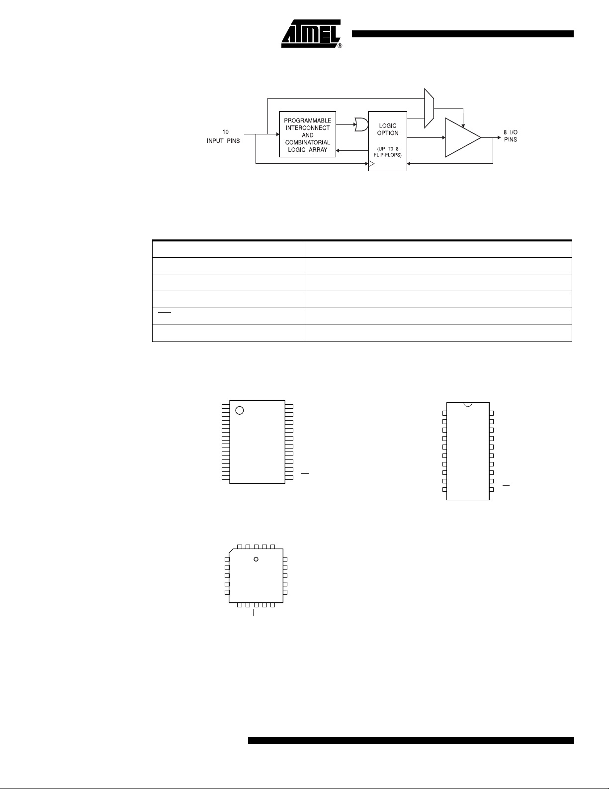
Figure 1-1. Block Diagram
2. Pin Configurations
Table 2-1. Pin Configurations (All Pinouts Top View)
Pin Name Function
CLK Clock
I Logic Inputs
I/O Bi-directional Buffers
OE
Output Enable
VCC +5V Supply
Figure 2-1. TSSOP Figure 2-2. DIP/SOIC
1
I/CLK
GND
2
I1
3
I2
4
I3
5
I4
6
I5
7
I6
8
I7
9
I8
10
VCC
20
I/O
19
I/O
18
I/O
17
I/O
16
I/O
15
I/O
14
I/O
13
I/O
12
I9/OE
11
I/CLK
GND
1
2
I1
3
I2
4
I3
5
I4
6
I5
7
I6
8
I7
9
I8
10
Figure 2-3. PLCC
I2I1I/CLK
VCC
I/O
321
20
19
18
I3
I4
I5
I6
I7
4
5
6
7
8
910111213
I8
GND
I9/OE
I/O
17
I/O
16
I/O
15
I/O
14
I/O
I/O
I/O
20
VCC
19
I/O
18
I/O
17
I/O
16
I/O
15
I/O
14
I/O
13
I/O
12
I/O
11
I9/OE
2
ATF16V8B/BQ/BQL
0364J–PLD–7/05
ATF16V8B/BQ/BQL
3. Absolute Maximum Ratings*
Temperature Under Bias.................................-55oC to +125oC
Storage Temperature ......................................-65
Voltage on Any Pin with
Respect to Ground .......................................-2.0 V to +7.0 V
o
C to +150oC
(1)
Voltage on Input Pins
with Respect to Ground
During Programming...................................-2.0 V to +14.0 V
Programming Voltage with
Respect to Ground .....................................-2.0 V to +14.0 V
(1)
(1)
4. DC and AC Operating Conditions
Operating Temperature (Ambient) 0
Power Supply 5V ± 5% 5V ± 10%
V
CC
*NOTICE: Stresses beyond those listed under “Absolute
Maximum Ratings” may cause permanent damage to the device. This is a stress rating only and
functional operation of the device at these or any
other conditions beyond those indicated in the
operational sections of this specification is not
implied. Exposure to absolute maximum rating
conditions for extended periods may affect device
reliability.
Note: 1. Minimum voltage is -0.6V DC, which may under-
shoot to -2.0V for pulses of less than 20 ns.
Maximum output pin voltage is V
which may overshoot to 7.0V for pulses of less
than 20 ns.
Commercial Industrial
o
C - 70oC-40
CC
o
C - 85oC
+ 0.75V DC,
0364J–PLD–7/05
3
4.1 DC Characteristics
Symbol Parameter Condition Min Typ Max Units
I
IL
Input or I/O Low
Leakage Current
0 ≤ V
≤ VIL(Max) -35 -100 µA
IN
I
IH
Input or I/O High
Leakage Current
3.5 ≤ V
IN
≤ V
CC
10 µA
Com. 55 85 mA
B-10
Ind. 55 95 mA
= Max,
V
I
CC
Power Supply
Current, Standby
CC
= Max,
V
IN
Outputs Open
B-15 Com. 50 75 mA
B-15 Ind. 50 80 mA
BQ-10 Com. 35 55 mA
BQL-15 Com. 5 10 mA
BQL-15 Ind. 5 15 mA
Com. 60 90 mA
B-10
Ind. 60 100 mA
B-15 Com. 55 85 mA
B-15 Ind. 55 95 mA
BQ-10 Com. 40 55 mA
I
CC2
Clocked Power
Supply Current
= Max,
V
CC
Outputs Open,
f = 15 MHz
BQL-15 Com. 20 35 mA
BQL-15 Ind. 20 40 mA
(1)
I
OS
V
IL
V
IH
V
OL
V
OH
Output Short
Circuit Current
= 0.5 V -130 mA
V
OUT
Input Low Voltage -0.5 0.8 V
Input High Voltage 2.0 VCC+0.75 V
V
Output High Voltage
Output High Voltage
= VIH or VIL,
IN
V
= Min
CC
= VIH or VIL,
V
IN
= Min
V
CC
IOL = -24 mA
Com., Ind.
= -4.0 mA 2.4 V
I
OH
0.5 V
Note: 1. Not more than one output at a time should be shorted. Duration of short circuit test should not exceed 30 sec.
4
ATF16V8B/BQ/BQL
0364J–PLD–7/05
ATF16V8B/BQ/BQL
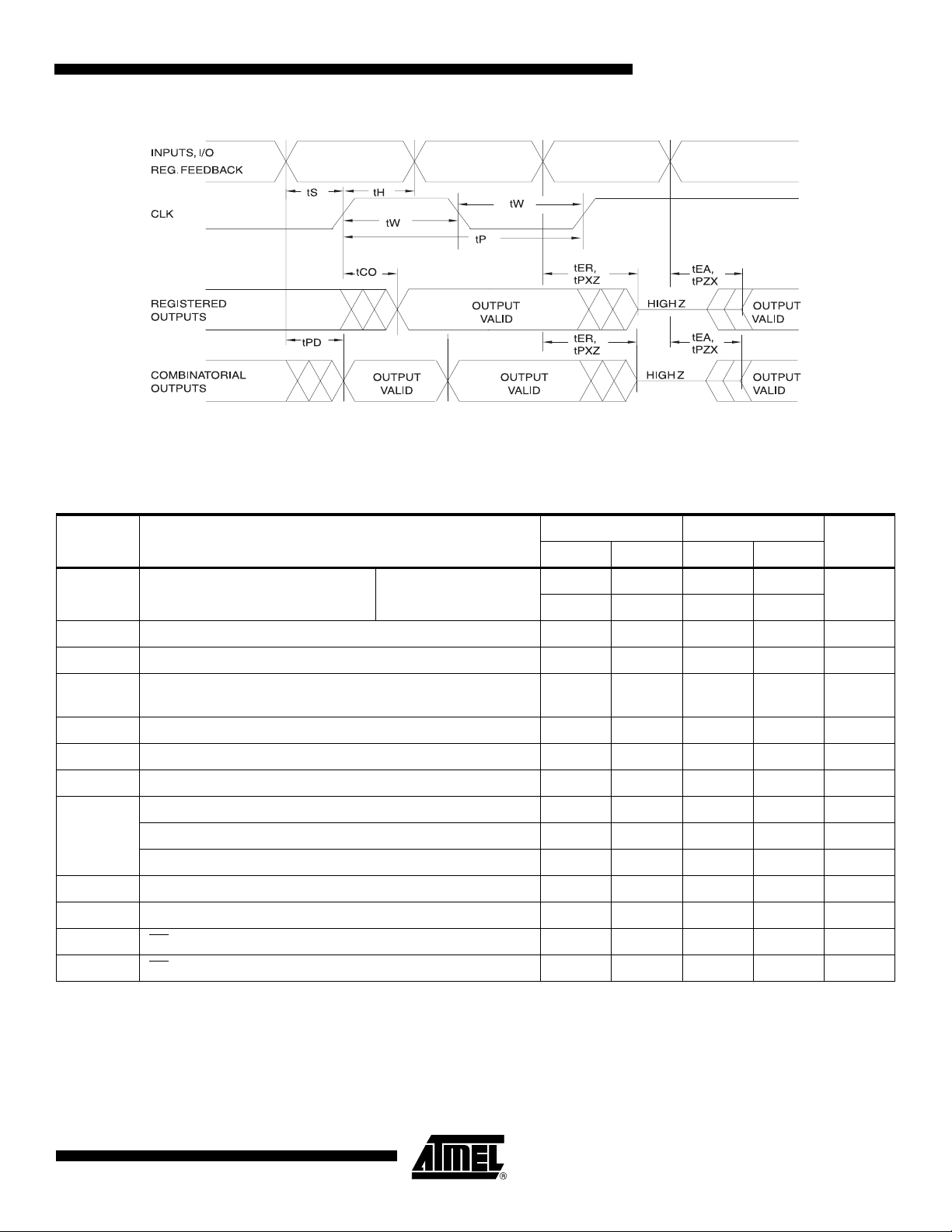
4.2 AC Waveforms
(1)
Note: 1. Timing measurement reference is 1.5V. Input AC driving levels are 0.0V 3.0V, unless otherwise
4.3 AC Characteristics
Symbol Parameter
specified.
(1)
-10 -15
UnitsMin Max Min Max
t
PD
t
CF
t
CO
t
S
t
H
t
P
t
W
Input or Feedback to
Non-Registered Output
8 outputs switching
Clock to Feedback 6 8 ns
Clock to Output 2 7 2 10 ns
Input or Feedback
Setup Time
Hold Time 0 0 ns
Clock Period 12 16 ns
Clock Width 6 8 ns
External Feedback 1/(tS + tCO)6845MHz
f
MAX
t
EA
t
ER
t
PZX
t
PXZ
Internal Feedback 1/(t
No Feedback 1/(t
Input to Output Enable — Product Term 3 10 3 15 ns
Input to Output Disable — Product Term 2 10 2 15 ns
OE pin to Output Enable 2 10 2 15 ns
OE pin to Output Disable 1.5 10 1.5 15 ns
+ tCF)7450MHz
S
)8362MHz
P
Note: 1. See ordering information for valid part numbers and speed grades.
310315
ns
7.5 12 ns
0364J–PLD–7/05
5
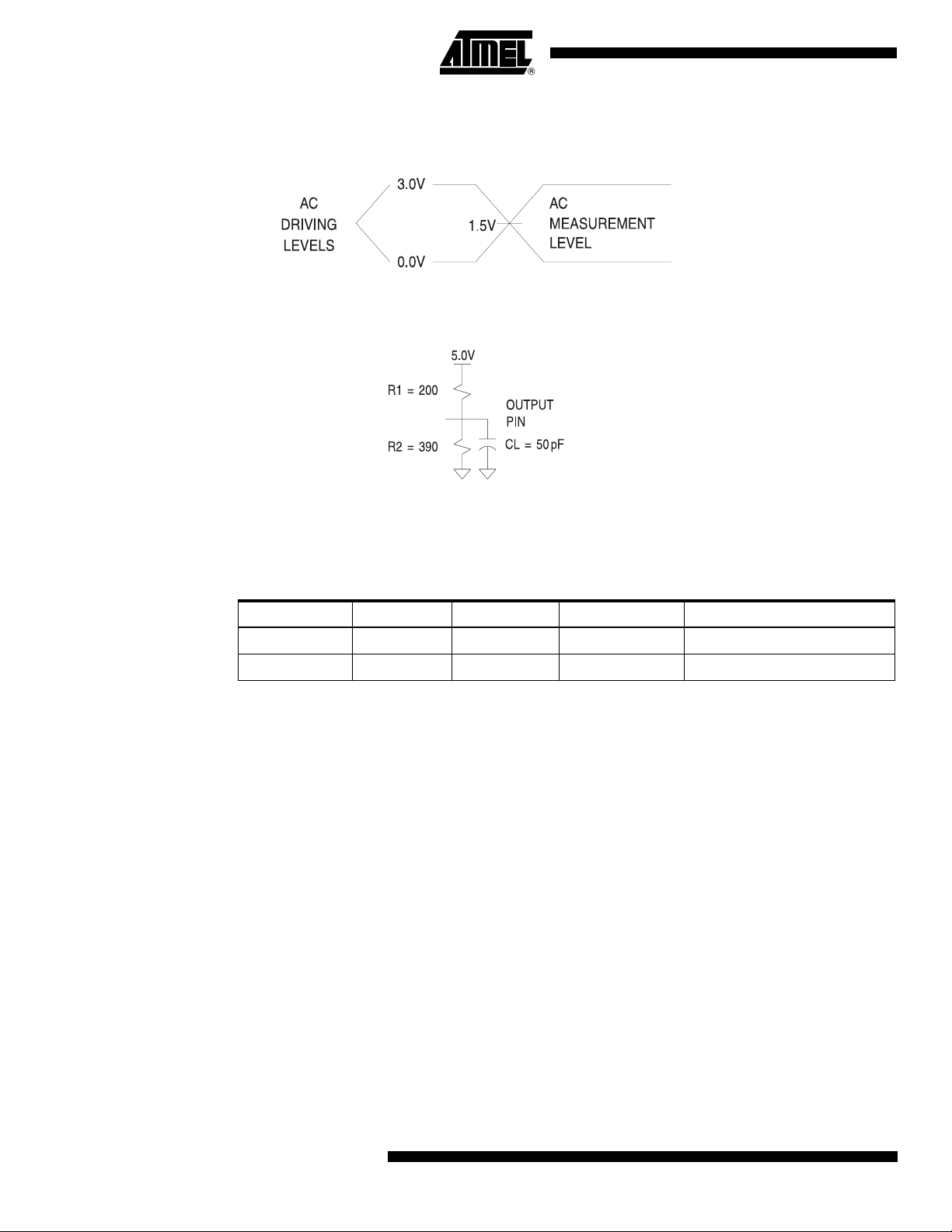
4.4 Input Test Waveforms
4.4.1 Input Test Waveforms and Measurement Levels
t
, tF < 5 ns (10% to 90%)
R
4.4.2 Output Test Loads (Commercial)
C
includes Test fixture and Probe capacitance
L
4.5 Pin Capacitance
Table 4-1. Pin Capacitance (f = 1 MHz, T = 25°C
Typ Max Units Conditions
C
IN
C
OUT
Note: 1. Typical values for nominal supply voltage. This parameter is only sampled and is not 100%
tested.
58 pF V
68 pF V
(1)
)
= 0V
IN
= 0V
OUT
6
ATF16V8B/BQ/BQL
0364J–PLD–7/05
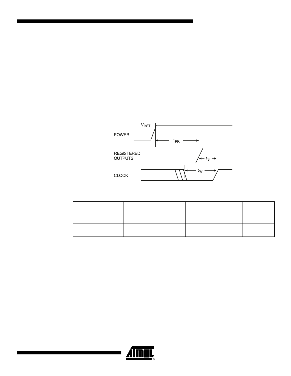
4.6 Power-up Reset
The registers in the ATF16V8Bs are designed to reset during power-up. At a point delayed
slightly from V
tered output state will always be high on power-up.
This feature is critical for state machine initialization. However, due to the asynchronous nature
of reset and the uncertainty of how V
required:
crossing V
CC
ATF16V8B/BQ/BQL
, all registers will be reset to the low state. As a result, the regis-
RST
actually rises in the system, the following conditions are
CC
1. The V
rise must be monotonic,
CC
2. After reset occurs, all input and feedback setup times must be met before driving the
clock pin high, and
3. The clock must remain stable during t
PR
.
Figure 4-1. Power-up Reset Waveforms
Table 4-2. Power-up Reset Parameters
Parameter Description Typ Max Units
t
PR
V
RST
Power-up
Reset Time
Power-up
Reset Voltage
600 1,000 ns
3.8 4.5 V
4.7 Preload of Registered Outputs
The ATF16V8B’s registers are provided with circuitry to allow loading of each register with either
a high or a low. This feature will simplify testing since any state can be forced into the registers
to control test sequencing. A JEDEC file with preload is generated when a source file with vectors is compiled. Once downloaded, the JEDEC file preload sequence will be done automatically
by most of the approved programmers after the programming.
5. Security Fuse Usage
A single fuse is provided to prevent unauthorized copying of the ATF16V8B fuse patterns. Once
programmed, fuse verify and preload are inhibited. However, the 64-bit User Signature remains
accessible.
The security fuse should be programmed last, as its effect is immediate.
0364J–PLD–7/05
7
6. Electronic Signature Word
There are 64 bits of programmable memory that are always available to the user, even if the
device is secured. These bits can be used for user-specific data.
7. Programming/Erasing
Programming/erasing is performed using standard PLD programmers. See CMOS PLD Programming Hardware and Software Support for information on software/programming.
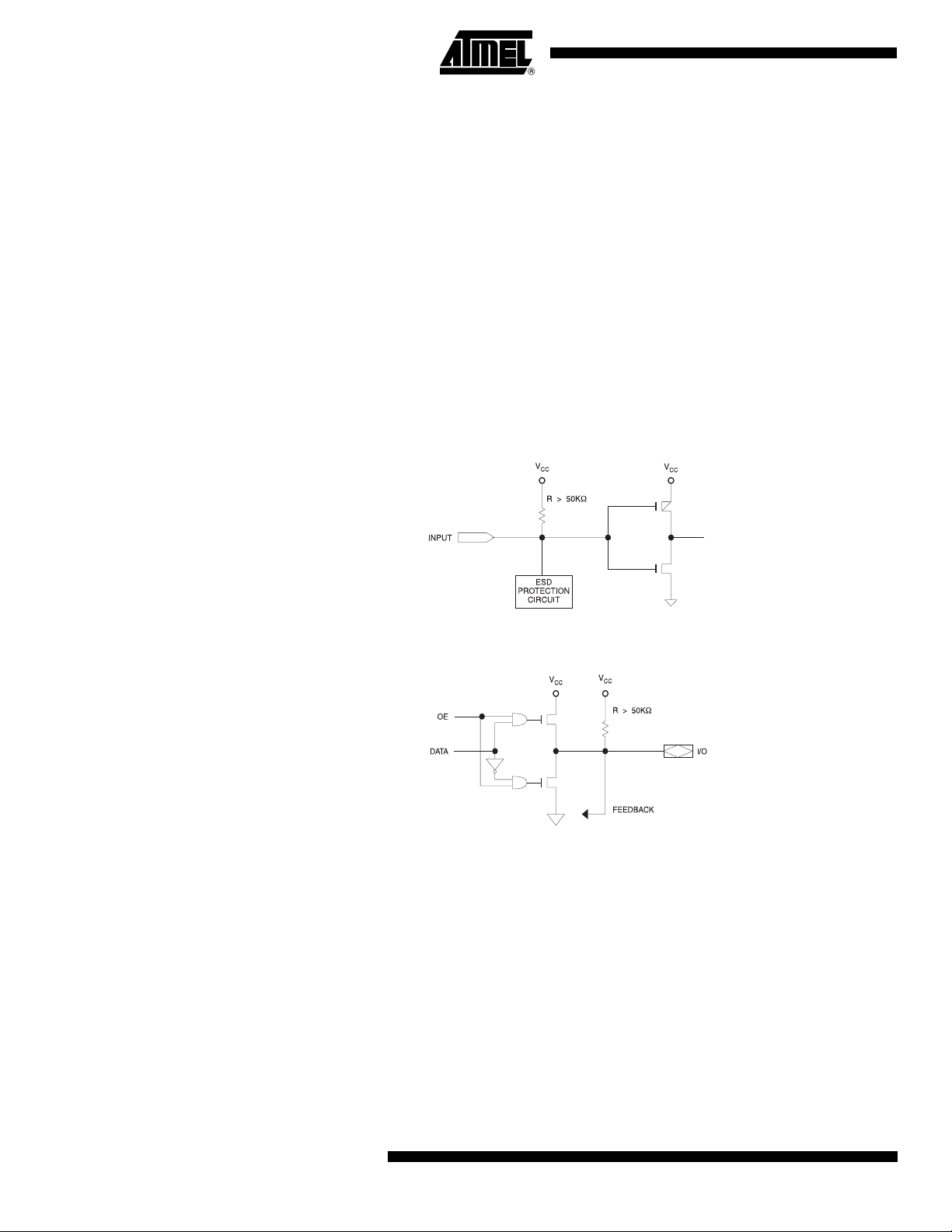
8. Input and I/O Pull-ups
All ATF16V8B family members have internal input and I/O pull-up resistors. Therefore, whenever inputs or I/Os are not being driven externally, they will float to V
logic array inputs are at known states. These are relatively weak active pull-ups that can easily
be overdriven by TTL-compatible drivers (see input and I/O diagrams below).
Figure 8-1. Input Diagram
. This ensures that all
CC
Figure 8-2. I/O Diagram
9. Functional Logic Diagram Description
The Logic Option and Functional Diagrams describe the ATF16V8B architecture. Eight configurable macrocells can be configured as a registered output, combinatorial I/O, combinatorial
output, or dedicated input.
The ATF16V8B can be configured in one of three different modes. Each mode makes the
ATF16V8B look like a different device. Most PLD compilers can choose the right mode automatically. The user can also force the selection by supplying the compiler with a mode selection.
The determining factors would be the usage of register versus combinatorial outputs and dedicated outputs versus outputs with output enable control.
The ATF16V8B universal architecture can be programmed to emulate many 20-pin PAL
devices. These architectural subsets can be found in each of the configuration modes described
8
ATF16V8B/BQ/BQL
0364J–PLD–7/05
 Loading...