

Page 1

查询ATF1516AS-10QC160供应商
Features
•
High Density, High Performance Electrically Erasable Complex
Programmable Logic Device
– 256 Macrocells
– 5 Product Terms per Macrocell, Expandable up to 40 per Macrocell
– 160, 192, 208-pins
– 10 ns Maximum Pin-to-Pin Delay
– Registered Operation Up To 100 MHz
– Enhanced Routing Resources
•
Flexible Logic Macrocell
– D/T/Latch Configurable Flip Flops
– Global and Individual Register Control Signals
– Global and Individual Output Enable
– Programmable Output Slew Rate
– Programmable Output Open Collector Option
– Maximum Logic utilization by burying a register within a COM output
•
Advanced Power Management Features
– Automatic 3 mA Stand-By for “L” Version (Max.)
– Pin-Controlled 4 mA Stand-By Mode (Typical)
– Programmable Pin-Keeper Inputs and I/Os
– Reduced-Power Feature Per Macrocell
•
Available in Commercial and Industrial Temperature Ranges
•
Available in 160-pin PQFP, 192 PGA and 208-pin RQFP Packages
•
Advanced EE Technology
– 100% Tested
– Completely Reprogrammable
– 100 Program/Erase Cycles
– 20 Year Data Retention
– 2000V ESD Protection
– 200 mA Latch-Up Immunity
•
JTAG Boundary-Scan Testing to IEEE Std. 1149.1-1990 and 1149.1a-1993 Supported
•
Fast In-System Programmability (ISP) via JTAG
•
PCI-compliant
•
3.3 or 5.0V I/O pins
•
Security Fuse Feature
High
Performance
EE-Based CPLD
ATF1516AS/L
Preliminary
Enhanced Features
•
Improved Connectivity (Additional Feedback Routing, Alternate Input Routing)
•
Output Enable Product Terms
•
D - Latch Mode
•
Combinatorial Output with Registered Feedback within any Macrocell
•
Three Global Clock Pins
•
ITD ( Input Transition Detection) Circuits on Global Clocks, Inputs and I/O
•
Fast Registered Input from Product Term
•
Programmable “Pin-Keeper” Option
•
VCC Power-Up Reset Option
•
Pull-Up Option on JTAG Pins TMS and TDI
•
Advanced Power Management Features
– Edge Controlled Power Down “L”
– Individual Macrocell Power Option
– Disable ITD on Global Clocks, Inputs and I/O
Rev. 0994A-A–01/98
1
Page 2
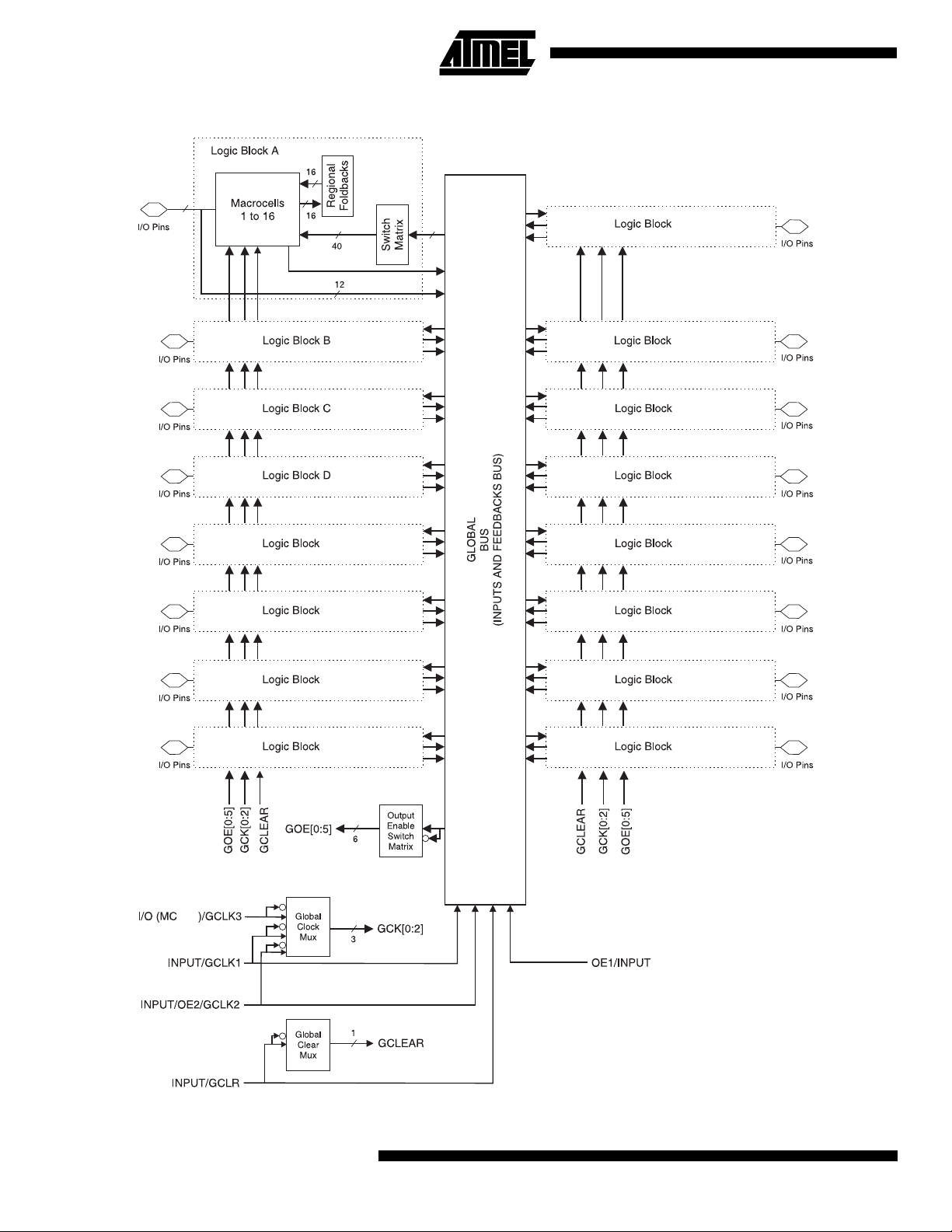
Block Diagram
6 to 12
P
O
N
M
256
E
F
G
H
L
K
J
I
2
ATF1516AS/L
Page 3
Description
The ATF1516AS is a high pe rforman ce, hig h densi ty Complex Programmable Logic Device (CPLD) which utilizes
Atmel’s proven el ectrical ly erasab le techno logy. W ith 256
logic macrocells and up to 164 inputs, it easily integrates
logic from several TTL, S SI, MSI, LSI and cl assic PLDs.
The ATF1516AS’s enhanced routing switch matrices
increase usable gate count, and incr ea se odds of successful pin-locked design modifications.
The ATF1516AS has up to 160 bi-directional I/O pins and 4
dedicated input pins, depending on the type of device package selected. Each dedicated pin can also serve as a global control signal; regi ster clock, r egister reset or output
enable. Each of these control signals can be selected for
use individually within each macrocell.
Each of the 256 mac rocells ge nerates a buried fe edback,
which goes to the gl obal bus . Each in put and I/O pin also
feeds into the global bus. The switch matrix in each logic
block then selects 40 individual signals from the global bus.
Each macrocell also generates a foldback logic term, which
goes to a regional bus. Casca de logi c between macro cells
in the ATF1516AS allows fa st, effici ent gen eration of complex logic func tions. The ATF15 16AS co ntains eigh t such
ATF1516AS/L
logic chains, each capable of creating sum term logic with a
fan in of up to 40 product terms
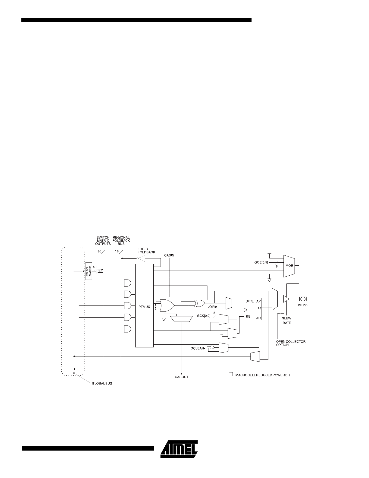
The ATF1516AS macrocel l, shown in F igure 1, is flexible
enough to support hi gh ly complex logic function s ope ratin g
at high speed. The macrocell consists of five sections:
product ter ms and product term select multiplexer;
OR/XOR/CASCADE logic; a flip-flop; output selec t and
enable; and logic array inputs.
Unused Macroc ell s are auto ma ticall y d isa bled by the compiler to decrease power consumption. A Security Fuse,
when programmed, protects the contents of the
ATF1516AS. Two bytes (16 bits) of User Signature are
accessible to the user for purposes such as storing project
name, part number, revision or date. The User Signature is
accessible regardless of the state of the Security Fuse.
The ATF1516AS device is an In-System Programmable
(ISP) device. It uses the industry standard 4-pi n JTAG
interface (IEEE Std. 1149.1), and is fully compliant with
JTAG’s Boundary Scan Description Language (BSDL). ISP
allows the device to be programmed witho ut removing it
from the printed circuit board. In addition to simplifying the
manufacturing flow, ISP also allows design modifications to
be made in the field via software.
Figure 1.
ATF1516AS Macrocell
3
Page 4

Product Terms and Select MUX
Each ATF1516AS macrocell has five product terms. Each
product term recei ve s a s its inp u ts al l s ig nal s f ro m bo th th e
global bus and regional bus.
The product term select multip lexer ( PTMUX ) alloc ates th e
five product terms as needed to the macrocell logic gates
and control signals. The PTMUX programming is determined by the design c ompiler, which se lects the opt imum
macrocell configuration.
OR/XOR/CASCADE Logic
The ATF1516AS’s logic structure is designed to efficiently
support all types of logic. Within a single macrocell, all the
product terms can be routed to the OR gate, creating a 5input AND/OR sum term. With the addition of the CASIN
from neighboring macrocells, this can be expanded to as
many as 40 product terms with a very small additional
delay.
The macrocell’s XOR gate allows efficient implementation
of compare and arithmetic func tions. O ne input to th e XOR
comes from the OR sum term. The other XOR input can be
a product term or a fixed high or low level. For combinatorial outputs, the fi xed level input allow s polarit y selecti on.
For registered functions, the fixed levels allow DeMorgan
minimization of product terms. The XOR gate is also used
to emulate T- and JK-type flip-flops.
Flip Flop
The ATF1516AS’s flip flop has very flexible data and control functions. The data input can come from either the
XOR gate, from a se parate prod uct term or directly fr om
the I/O pin. Selecting the separate product term allows creation of a buried registered feedback within a combinatorial
output macrocell. (This feature is automatically implemented by the fitter so ftware). I n add ition to D , T, J K and
SR operation, the flip flop can also be configured as a flowthrough latch. In this mode, da ta passes th rough whe n the
clock is high and is latched when the clock is low.
The clock itself can eith er be th e Global CLK Si gnal ( GCK)
or an individual product term. The flip flop changes state on
the clock’s rising edge. When the GCK signal is used as
the clock, one of the macrocell product terms can be
selected as a clock enable. When the clock enable function
is active and the enable signal (product term) is low, all
clock edges are ignored. The flip flop’s asynchro nous re se t
signal (AR) can be either the Global Clear (G CLEAR), a
product term, or always o ff. AR can also be a logi c OR of
GCLEAR with a product term. The as ynchronous prese t
(AP) can be a product term or always off.
Output Select and Enable
The ATF1516AS macrocell output can be selected as registered or combinatorial. The buried feedback signal can be
either combinatorial or registered signal regardless of
whether the output is combinatorial or registered.
The output enable multiplexer (MOE) controls the output
enable signals . Any buffer ca n be perman ently enab led for
simple output operation. Buffers ca n also be permanently
disabled to allow use of the pin as an i nput. In this confi guration all the ma croce ll res our ces are still ava ilab le, i ncl uding the buried feedback, expan der and CASCADE logic .
The output enable for each macrocell can be selected as
either of the two dedicated OE input pins as an I/O pin configured as an input, or as an individual product term.
Global Bus/Switch Matrix
The global bus contains all input and I/O pin signals as well
as the buried fe edback signal from all 256 mac rocells.
The Switch Matrix in ea ch Logic Block receives as its
inputs all signals from the global bus. Under software control, up to 40 of these signals can be selected as inputs to
the Logic Block.
Foldback Bus
Each macrocell a lso generate s a foldbac k product ter m.
This signal goes to the regional bus and is available to 16
macrocells. The foldback is an inverse polarity of one of the
macrocell’s product terms. T he 16 foldback te rms in eac h
region allows generation of hi gh fan -in su m ter ms (up to 21
product terms) with a small additional delay.
4
ATF1516AS/L
Page 5

ATF1516AS/L
Programmable Pin-Keeper Option
for Inputs and I/Os
The ATF1516AS offers the option of program ming all input
and I/O pins so that “pin keeper” circuits can be utilized.
When any pin is driven high or low and then subsequently
left floating, it will stay at that previous high or low leve l.
This circuitry preve nts unused input and I/O l ines from
floating to intermedi ate volta ge levels , which caus e unnecessary power consumption and system noise. The keeper
circuits eliminate the need for external pull-up resistors and
eliminate their DC power consumption.
Input Diagram
I/O Diagram
macrocells to be configured for maximum power savings.
This feature may be selected as a design option.
All ATF1516ASs also have an opti onal pow er down mode .
In this mode, current drops to below 10 mA. When the
power down opti on is select ed, eit her PD1 or PD2 pins (or
both) can be used to power down the part. The power down
option is selected in the design source fil e. When en abled,
the device goes into power down when either PD1 or PD2
is high. In the power down mod e, all inter nal logic signals
are latched and held, as are any enabled outputs.
All pin transitions are ignored until the PD pin is brought
low. When the power down feature is enabled, the PD1 or
PD2 pin cannot be used as a logic input or output. However, the pin’s macroc ell m ay still be u sed to g enera te buried foldback and cascade logic signals.
All Power-Down AC Character istic parameters are c omputed from external input or I/O pins, with Reduced Power
Bit turned on. For mac rocells in reduced-po wer mode
(Reduced power bit turned on), the reduced power adder,
tRPA, must be adde d to the AC p arameter s, w hich includ e
, t
the data paths t
Each output also has in divi dual sl ew rate contr ol. This may
be used to reduce system noise by slowing down o utputs
that do not need to operate at maximum speed. Outputs
default to slow switching, and may be specified as fas t
switching in the design file.
LAD
LAC
, tIC, t
ACL
, t
ACH
and t
SEXP
.
Design Software Support
ATF1516AS designs are supported by several third party
tools. Automated fitters allow logic synthesis using a variety
of high level description languages and formats.
Speed/Power Management
The ATF1516AS has several built-in speed and power
management features. The ATF1516A S contains circui try
that automatically puts the device into a low power standby mode when no logic trans itions are occ urring. This n ot
only reduces power consumption during inactive periods,
but also provide s a proportional po wer savings for m ost
applications running at system speeds below 50 MHz.
To further reduce power, each ATF1516AS macrocell has
a Reduced Power bit f eatu re . Thi s feat ure al lo ws in div id ual
Power Up Reset
The ATF1516AS has a power -up re set opt ion at t wo di fferent voltage trip levels when the device is being powered
down. Within the fitter, or during a conversion, if the
“power-reset” option is turned “on” (which is the default
option), the trip levels du ring power up or power down is at
2.8V. The user can change this default option from “on” to
“off” (within the fitter or specify it as a switch during conversion). When this is done, the voltage trip level during
power-down changes from 2.8V to 0.7V. This is to ensure a
robust operating enviro nme nt.
The registers in the ATF1516AS are designed to re se t du ring power up. At a poin t dela ye d slight ly fr om V
, all registers will be reset to the low state. The output
V
RST
state will depend on the polarity of the buffer.
This feature is critical for s tate machin e initi alizati on. How-
ever, due to the asynchronous nature of reset and the
uncertainty of h ow V
lowing conditions are required:
actually rises in the sys tem, the fo l-
CC
crossing
CC
5
Page 6

1. The V
2. After reset occurs, all input and feedback setup times
must be met before driving the clock pin high, and,
3. The clock must remain stable during T
rise must be monotonic,
CC
PR
.
Security Fuse Usage
A single fuse is provided to pre vent unauthorize d copying
of the ATF1516AS fuse patterns. Once programmed, fuse
verify is inhibited. However, User Signature and device ID
remains accessib le.
Programming
ATF1516AS devices are In-System Programmable (ISP)
devices utilizing the 4-pin JTAG protocol. Thi s capability
eliminates packa ge h andl in g no rm all y requ ire d for pr ogra m
and facilitates rapid design iterations and field changes.
Atmel provides ISP hardware and software to allow programming of the ATF1516AS via the PC. ISP is perfomed
by using either a download c able, or a compar able board
tester or a simple microprocessor interface.
To facilitate ISP programmi ng by the Automated Test
Equipment (ATE) vendors. Serial Vector Format (SVF)
files can be created by Atmel provided Software utilities.
ATF1516AS devices can also be programmed using standard 3rd party programmers. With 3rd party programmer
the JTAG ISP port can be disabled thereby allowing 4 additional I/O pins to be used for logic.
Contact your local Atmel representativ es or Atmel PLD
applications for details.
ISP Programming Protection
The ATF1516AS ha s a special featur e which locks the
device and prevents the inputs and I/O from drivi ng if the
programming process is interrupted due to any reason. The
inputs and I/O default to high-Z state during such a condition. In addition the pin keep er option pres erves t he f ormer
state during device programming.
All ATF1516AS devices ar e initially s hipped in the er ased
state thereby making them ready to use for ISP.
Note: For more information refer to the “Desigining for In-Sys-
tem Programmability with Atmel CPLDs” application
note.
Timing Model
U
6
ATF1516AS/L
Page 7

ATF1516AS/L
Input Test W aveforms and
Measurement Levels
rR, tF = 1.5 ns typical
Power Down Mode
The ATF1516AS includes two pins for optional pin controlled power down feature. When this mode is enabled, the
PD pin acts as the power down pin. When the PD1 and
PD2 pin is high, the device supply current is reduced to
less than 3 mA. During power down, all outp ut data and
internal logic states are latched and held. Therefore, all
registered and co mbin atoria l output da ta remai n valid. Any
outputs which were in a Hi-Z state at the onset will remain
at Hi-Z. During power down, all input si gnals except th e
power down p in are block ed. Input an d I/O hold l atches
remain active to insure that pins do not float to indete rminate levels, further r educing system po wer. The power
down pin feature is enabled in the logic design file. Designs
using either power down pin may not use the PD pin logic
array input. However, all other PD pin as macrocell
resources may still be used, including the buried feedback
and foldback product term array inputs.
Output AC Test Loads:
(3.0V)*
(703 )*
(8060 )*
Note: *Numbers in parenthesis refer to 3.0V operating condi-
tions (preliminary).
7
Page 8

JTAG-BST Overview
The JTAG boundary-scan testing is controlled by the Test
Access Port (TAP) controller in the ATF1516AS. The
boundary-scan technique involves the inclusion of a shiftregister stage (conta ined in a b oun dary-sc an cell) ad jacen t
to each component so that signals at component boundaries can be controlle d and observed us ing scan testin g
principles. Each inp u t pin and I/O pin has its own boundary
scan cell (BSC) in order to support boundary scan testing.
The ATF1516AS does not currently include a Test Reset
(TRST) input pi n because th e TAP contr oller is aut omatically reset at power up. The six JTAG BST modes supported include: SAMPLE/PRELOAD, EXTEST, BYPASS,
IDCODE. BST on the ATF1516A S is implemented u sing
the Boundary Sc an Definiti on Langu age (BSD L) desc ribed
in the JTAG specification (IEEE Standard 1149.1). Any
third party tool that suppo rts the BS DL format can be used
to perform BST on the ATF1516AS.
The ATF1516A S also ha s the opti on of usi ng four JTA Gstandard I/O pins for in-system programming (ISP). The
ATF1516AS is programmable through the four JTAG pins
using programming compatible with the IEEE JTAG Standard 1149.1. Programming is performed by using 5V TTLlevel programming signals fr om the JTAG ISP inter face.
The JTAG feature is a progr am mab le opti on. If J TAG (BS T
or ISP) is not needed, then the four JTAG control pins are
available as I/O pins.
BSC Configuration Pins and
Macrocells (except JTAG TAP Pins)
Note: The ATF1516AS has pull-up option on TMS and TDI
pins. This feature is selected as a design option.
JTAG Boundary Scan Cell (BSC)
Testing
The ATF1516AS contains up to 160 I/O pins and 4 input
pins, depending on the device type and package ty pe
selected. Each input pi n and I/O pin has its own bounda ry
scan cell (BSC) in order to suppor t boundary sca n testing
as described in detail by IEEE Standard 1149.1. Typical
BSC consis ts of thre e capture registe rs or sca n regist ers
and up to two update registers. There are two types of
BSCs, one for input or I/O pin, and one for the macrocells.
The BSCs in the device are chain ed together through the
capture registers. Input to the capture register chain is fed
in from the TDI pin while the output is directed to the TDO
pin. Capture re gisters a re used to capture ac tive de vice
data signals, to shift data in and out of the device and to
load data into the update registers. Control signals are generated internally by the JTAG TAP controller. The BSC
configurati on for th e input and I/O pins a nd macr ocells are
shown below.
8
ATF1516AS/L
Page 9

BSC Configuration for Macrocell
ATF1516AS/L
Pin BSC
TDO
OEJ
Pin
0
1
DQ
Capture
DR
TDI
Clock
Shift
TDO
0
0
1
DQ
DQ
1
OUTJ
TDI
Shift
0
0
1
DQ
Capture
DR
DQ
Update
DR
1
Pin
Mode
Clock
Macrocell BSC
9
Page 10

PCI Compliance
The ATF1516AS also supports the growing need in the
industry to support the new Peripheral Component Interconnect (PCI) interface standard in PCI-based designs and
specifications . The PCI interfac e calls for high curre nt drivers which are much larger than the traditional TTL drivers.
PCI Voltage-to-Current Curv es for +5V
Signaling in Pull-Up Mode
point
Pull Up
-44
Current (mA)
Test Point
-178
VCC
2.4
1.4
Voltage
DC
drive point
AC drive
-2
PCI Voltage-to-Current Curves for +5V
Signaling in Pull-Down Mode
VCC
Voltage
2.2
DC
drive point
0.55
3.6
AC drive
point
Pull Down
95
Test Point
Current (mA)
380
10
ATF1516AS/L
Page 11

Ordering Information
t
PD
(ns)
t
CO1
(ns)
f
MAX
(MHz) Ordering Code Package Operation Range
ATF1516AS/L
10 5 125 ATF1516AS-10QC160
ATF1516AS-10UC192
ATF1516AS-10QHC208
15 8 100 ATF1516AS-15QC160
ATF1516AS-15UC192
ATF1516AS-15QHC208
15 8 100 ATF1516AS-15Q160
ATF1516AS-15UI192
ATF1516AS-15QHI208
20 12 83.3 ATF1516ASL-20QC160
ATF1516ASL-20UC192
ATF1516ASL-20QHC208
20 12 83.3 ATF1516ASL-20QI160
ATF1516ASL-20UI192
ATF1516ASL-20QHI208
25 15 70 ATF1516ASL-25QC160
ATF1516ASL-25UC192
ATF1516ASL-25QHC208
25 15 70 ATF1516ASL-25QI60
ATF1516ASL-25UI192
ATF1516ASL-25QHI208
160Q
192U
208QH
160Q
192U
208QH
160Q
192U
208QH
160Q
192U
208QH
160Q
192U
208QH
160Q
192U
208QH
160Q
192U
208QH
Commercial
(0°C to 70°C)
Commercial
(0°C to 70°C)
Industrial
(-40°C to +85°C)
Commercial
(0°C to 70°C)
Industrial
(-40°C to +85°C)
Commercial
(0°C to 70°C)
Industrial
(-40°C to +85°C)
160Q
192U
208QH
Package Type
160-Lead, Plastic Quad FlatPack (PQFP)
192-Lead, Plastic Grid Array (PGA)
208-Lead, Plastic Quad Flatpack with Heat Spreader (RQFP)
11
 Loading...