


BDTIC www.bdtic.com/ATMEL
Features
• High-density, High-performance, Electrically-erasable Complex Programmable
Logic Device
– 64 Macrocells
– 5 Product Terms per Macrocell, Expandable up to 40 per Macrocell
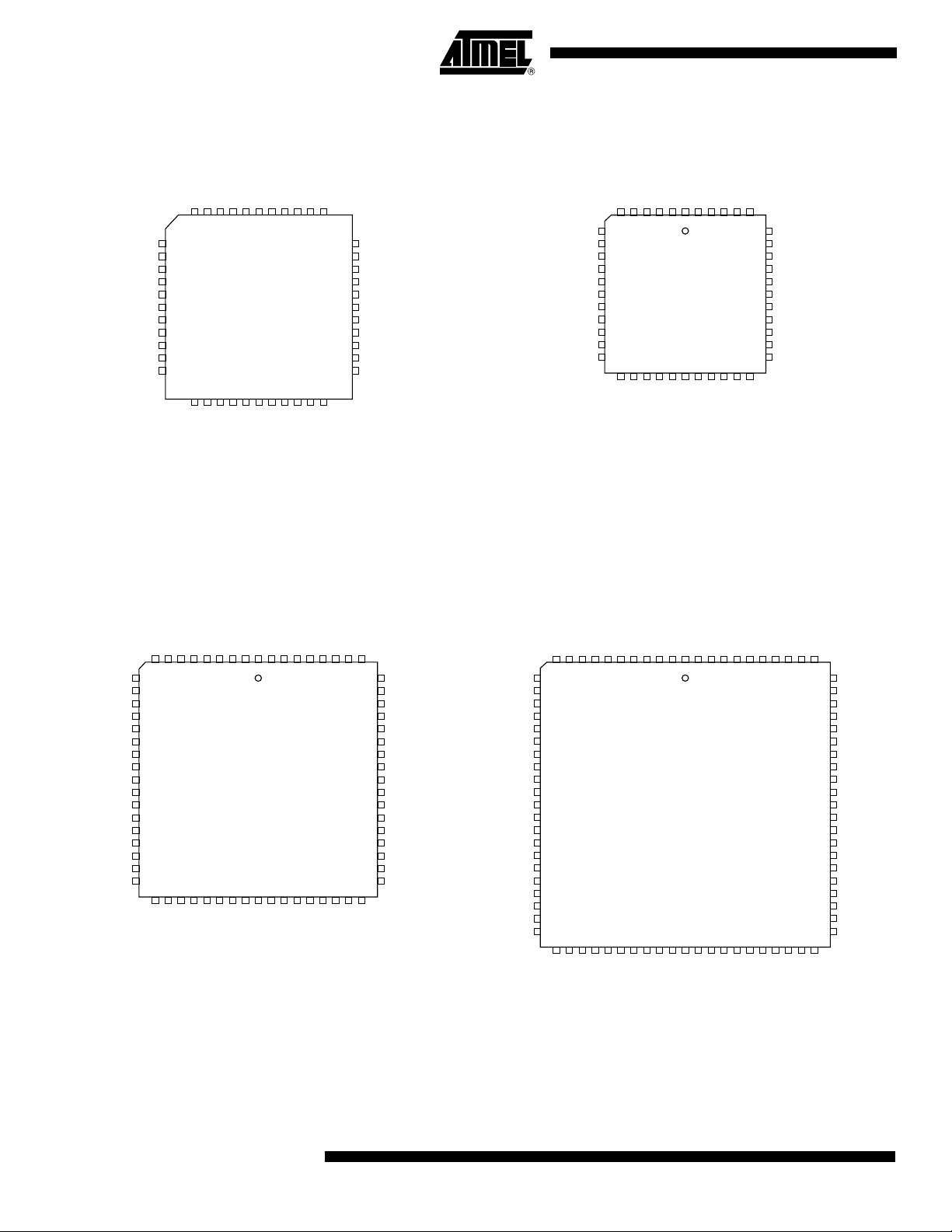
– 44, 68, 84, 100 Pins
– 7.5 ns Maximum Pin-to-pin Delay
– Registered Operation up to 125 MHz
– Enhanced Routing Resources
• In-System Programmability (ISP) via JTAG
• Flexible Logic Macrocell
– D/T/Latch Configurable Flip-flops
– Global and Individual Register Control Signals
– Global and Individual Output Enable
– Programmable Output Slew Rate
– Programmable Output Open Collector Option
– Maximum Logic Utilization by Burying a Register with a COM Output
• Advanced Power Management Features
– Automatic µA Standby for “L” Version
– Pin-controlled 1 mA Standby Mode
– Programmable Pin-keeper Circuits on Inputs and I/Os
– Reduced-power Feature per Macrocell
• Available in Commercial and Industrial Temperature Ranges
• Available in 44-, 68-, and 84-lead PLCC; 44- and 100-lead TQFP; and 100-lead PQFP
• Advanced EE Technology
– 100% Tested
– Completely Reprogrammable
– 10,000 Program/Erase Cycles
– 20-year Data Retention
– 2000V ESD Protection
– 200 mA Latch-up Immunity
• JTAG Boundary-scan Testing to IEEE Std. 1149.1-1990 and 1149.1a-1993 Supported
• PCI-compliant
• 3.3V or 5.0V I/O Pins
• Security Fuse Feature
• Green (Pb/Halide-fee/RoHS Compliant) Package Options
Highperformance
Complex
Programmable
Logic Device
ATF1504AS
ATF1504ASL
Enhanced Features
• Improved Connectivity (Additional Feedback Routing, Alternate Input Routing)
• Output Enable Product Terms
• Transparent – Latch Mode
• Combinatorial Output with Registered Feedback within Any Macrocell
• Three Global Clock Pins
• ITD (Input Transition Detection) Circuits on Global Clocks, Inputs and I/O
• Fast Registered Input from Product Term
• Programmable “Pin-keeper” Option
• V
Power-up Reset Option
CC
• Pull-up Option on JTAG Pins TMS and TDI
• Advanced Power Management Features
– Edge-controlled Power-down “L”
– Individual Macrocell Power Option
– Disable ITD on Global Clocks, Inputs and I/O
Rev. 0950O–PLD–7/05
1
I/O/TDI
GND
PD1/I/O
TMS/I/O
VCC
44-lead TQFP
Top View
I/O
I/O
I/O
VCC
GCLK2/OE2/I
GCLR/I
I/OE1
GCLK1/I
GND
GCLK3/I/O
I/O
4443424140393837363534
33
1
2
I/O
3
I/O
4
5
6
I/O
7
8
I/O
9
10
I/O
11
I/O
1213141516171819202122
I/O
I/O
I/O
I/O
I/O
I/O
GND
VCC
I/O
PD2/I/O
I/O
32
I/O/TDO
31
I/O
30
I/O
29
VCC
28
I/O
27
I/O
26
I/O/TCK
25
I/O
24
GND
23
I/O
I/O
TDI/I/O
I/O
I/O
GND
PD1/I/O
I/O
I/O/TMS
I/O
VCC
I/O
I/O
44-lead PLCC
Top View
I/O
I/O
I/O
VCC
GCLK2/OE2/I
GCLR/I
OE1/I
GCLK1/I
65432
7
8
9
10
11
12
13
14
15
16
17
1819202122232425262728
I/O
I/O
1
4443424140
I/O
I/O
I/O
VCC
GND
PD2/I/O
GND
GCLK3/I/O
I/O
I/O
I/O
39
I/O
38
I/O/TDO
37
I/O
36
I/O
35
VCC
34
I/O
33
I/O
32
I/O/TCK
31
I/O
30
GND
29
I/O
I/O
VCCIO
I/O/TD1
GND
I/O/PD1
I/O/TMS
VCCIO
GND
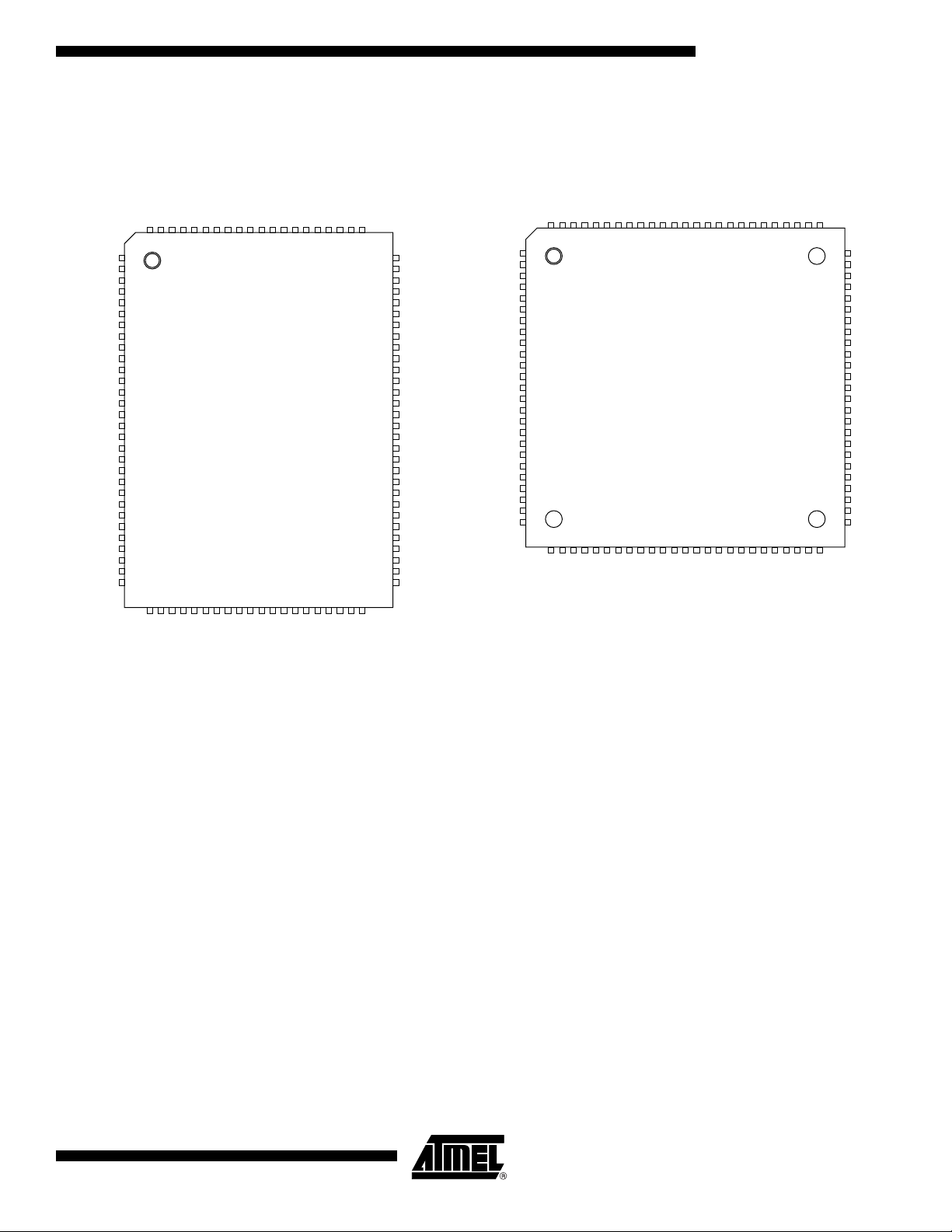
68-lead PLCC
Top View
I/O
I/O
I/O
GND
I/O
I/O
VCCINT
GCLK2/OE2/I
GCLR/I
OE1/I
987654321
10
I/O
11
12
13
I/O
14
I/O
15
I/O
16
17
18
I/O
19
20
I/O
21
22
I/O
23
I/O
24
I/O
25
I/O
26
2728293031323334353637383940414243
I/O
I/O
I/O
I/O
I/O
VCCIO
I/O
GND
VCCINT
68676665646362
I/O
GCLK1/I
GND
GND
I/O/PD2
GCLK3/I/O
I/O
VCCIO
I/O
I/O
I/O
I/O
I/O
I/O
61
60
59
58
57
56
55
54
53
52
51
50
49
48
47
46
45
44
VCCIO
I/O
I/O
GND
I/O/TDO
I/O
I/O
I/O
VCCIO
I/O
I/O
I/O/TCK
I/O
GND
I/O
I/O
I/O
I/O
VCCIO
I/O/TDI
GND
I/O/PD1
I/O/TMS
VCCIO
GND
84-lead PLCC
Top View
I/O
I/O
I/O
I/O
GND
I/O
I/O
I/O
VCCINT
GCLK2/OE2/I
I/GCLR
I/OE1
GCLK1/I
GND
987654321
11
10
12
I/O
13
14
15
I/O
16
I/O
17
I/O
18
I/O
19
20
21
I/O
22
I/O
23
24
I/O
25
I/O
26
27
I/O
28
I/O
29
I/O
30
I/O
31
I/O
32
333435363738394041424344454647484950515253
I/O
I/O
I/O
I/O
I/O
I/O
I/O
VCCIO
848382818079787776
I/O
I/O
I/O
GND
VCCINT
I/O/PD2
GCLK3/I/O
I/O
I/O
I/O
I/O
GND
VCCIO
1/O
I/O
I/O
I/O
I/O
I/O
75
74
73
72
71
70
69
68
67
66
65
64
63
62
61
60
59
58
57
56
55
54
VCCIO
I/O
I/O
GND
I/O/TDO
I/O
I/O
I/O
I/O
VCCIO
I/O
I/O
I/O
I/O/TCK
I/O
I/O
GND
I/O
I/O
I/O
I/O
I/O
2
ATF1504AS(L)
0950O–PLD–7/05
ATF1504AS(L)
VCCIO
I/O/TDI
GND
I/O/PD1
I/O/TMS
VCCIO
GND
100-lead PQFP
Top View
I/O
I/O
I/O
I/O
I/O
GND
I/O
I/O
I/O
VCCINT
INPUT/OE2/GCLK2
INPUT/GCLR
INPUT/OE1
INPUT/GCLK1
GND
I/O/GCLK3
I/O
I/O
VCCIO
I/O
I/O
I/O
99989796959493929190898887868584838281
100
1
NC
2
NC
3
I/O
4
I/O
5
6
7
NC
8
I/O
9
NC
10
I/O
11
I/O
12
I/O
13
14
15
I/O
16
I/O
17
18
I/O
19
I/O
20
21
I/O
22
I/O
23
I/O
24
NC
25
I/O
26
NC
27
I/O
28
29
NC
30
NC
31323334353637383940414243444546474849
I/O
I/O
I/O
I/O
I/O
I/O
I/O
I/O
I/O
I/O
I/O
VCCIO
GND
VCCINT
GND
I/O/PD2
I/O
80
NC
79
NC
78
I/O
77
I/O
76
GND
75
I/O/TDO
74
NC
73
I/O
72
NC
71
I/O
70
I/O
69
I/O
68
VCCIO
67
I/O
66
I/O
65
I/O
64
I/O/TCK
63
I/O
62
I/O
61
GND
60
I/O
59
I/O
58
I/O
57
NC
56
I/O
55
NC
54
I/O
53
VCCIO
52
NC
51
NC
50
I/O
I/O
I/O
VCCIO
I/O/TDI
GND
I/O/PD1
I/O/TMS
VCCIO
NC
1
NC
2
3
4
NC
5
I/O
6
NC
7
I/O
8
I/O
9
I/O
10
11
12
I/O
13
I/O
14
15
I/O
16
I/O
17
18
I/O
19
I/O
20
I/O
21
NC
22
I/O
23
NC
24
I/O
25
I/O
9998979695949392919089888786858483828180797877
100
26272829303132333435363738394041424344454647484950
NC
NC
GND
100-lead TQFP
I/O
I/O
GND
I/O
I/O
I/O
I/O
I/O
I/O
I/O
Top View
I/O
VCCINT
INPUT/OE2/GCLK2
INPUT/GCLR
I/O
I/O
I/O
VCCIO
INPUT/OE1
INPUT/GCLK1
GND
I/O
GND
VCCINT
I/O/GCLK3
I/O
I/O
I/O
GND
I/O/PD2
VCCIO
I/O
I/O
I/O
I/O
I/O
I/ONCNC
I/O
I/O
I/O
76
I/O
75
GND
74
I/O/TDO
73
NC
72
I/O
71
NC
70
I/O
69
I/O
68
I/O
67
VCCIO
66
I/O
65
I/O
64
I/O
63
I/O/TCK
62
I/O
61
I/O
60
GND
59
I/O
58
I/O
57
I/O
56
NC
55
I/O
54
NC
53
I/O
52
VCCIO
51
NC
NC
0950O–PLD–7/05
3

Description The ATF1504AS is a high-performance, high-density complex programmable logic
device (CPLD) that utilizes Atmel’s proven electrically-erasable memory technology.
With 64 logic macrocells and up to 68 inputs, it easily integrates logic from several TTL,
SSI, MSI, LSI and classic PLDs. The ATF1504AS’s enhanced routing switch matrices
increase usable gate count and the odds of successful pin-locked design modifications.
The ATF1504AS has up to 68 bi-directional I/O pins and four dedicated input pins,
depending on the type of device package selected. Each dedicated pin can also serve
as a global control signal, register clock, register reset or output enable. Each of these
control signals can be selected for use individually within each macrocell.
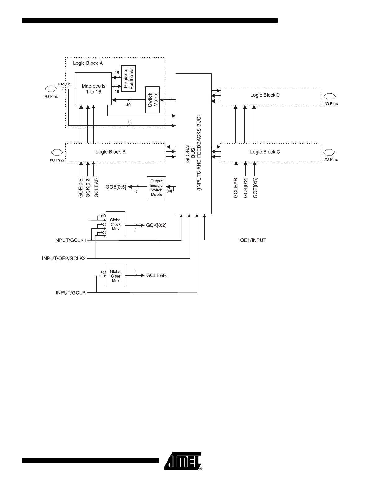
Each of the 64 macrocells generates a buried feedback that goes to the global bus.
Each input and I/O pin also feeds into the global bus. The switch matrix in each logic
block then selects 40 individual signals from the global bus. Each macrocell also generates a foldback logic term that goes to a regional bus. Cascade logic between
macrocells in the ATF1504AS allows fast, efficient generation of complex logic functions. The ATF1504AS contains four such logic chains, each capable of creating sum
term logic with a fan-in of up to 40 product terms.
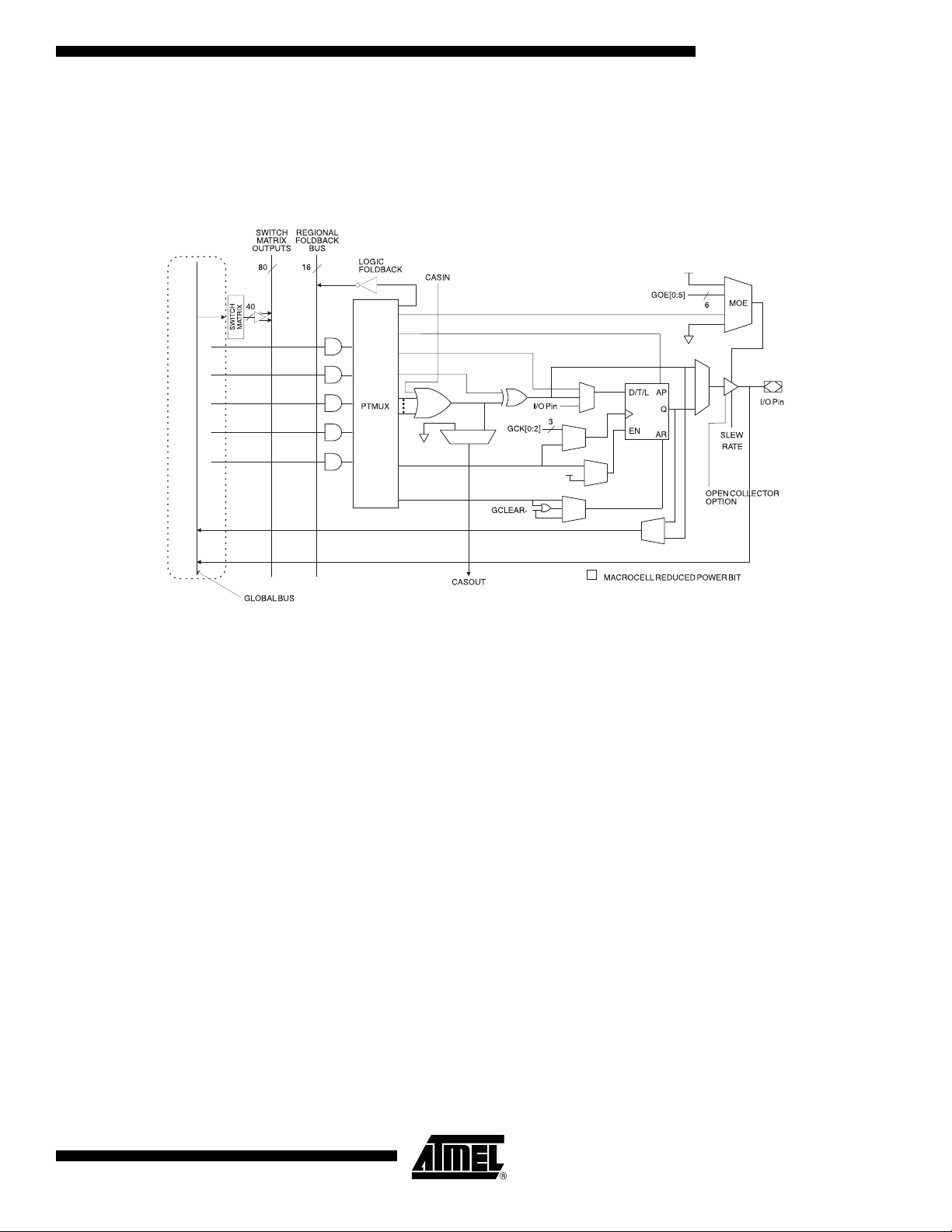
The ATF1504AS macrocell, shown in Figure 1, is flexible enough to support highly-complex logic functions operating at high speed. The macrocell consists of five sections:
product terms and product term select multiplexer, OR/XOR/CASCADE logic, a flip-flop,
output select and enable, and logic array inputs.
4
ATF1504AS(L)
0950O–PLD–7/05
Block Diagram
ATF1504AS(L)
I/O (MC64)/GCLK3
Unused product terms are automatically disabled by the compiler to decrease power
consumption. A security fuse, when programmed, protects the contents of the
ATF1504AS. Two bytes (16 bits) of User Signature are accessible to the user for purposes such as storing project name, part number, revision or date. The User Signature
is accessible regardless of the state of the security fuse.
The ATF1504AS device is an in-system programmable (ISP) device. It uses the industry-standard 4-pin JTAG interface (IEEE Std. 1149.1), and is fully-compliant with JTAG’s
Boundary-scan Description Language (BSDL). ISP allows the device to be programmed
without removing it from the printed circuit board. In addition to simplifying the manufacturing flow, ISP also allows design modifications to be made in the field via software.
0950O–PLD–7/05
5

Product Terms and Select Mux
OR/XOR/CASCADE Logic The ATF1504AS’s logic structure is designed to efficiently support all types of logic.
Flip-flop The ATF1504AS’s flip-flop has very flexible data and control functions. The data input
Each ATF1504AS macrocell has five product terms. Each product term receives as its
possible inputs all signals from both the global bus and regional bus.
The product term select multiplexer (PTMUX) allocates the five product terms as
needed to the macrocell logic gates and control signals. The PTMUX programming is
determined by the design compiler, which selects the optimum macrocell configuration.
Within a single macrocell, all the product terms can be routed to the OR gate, creating a
5-input AND/OR sum term. With the addition of the CASIN from neighboring macrocells,
this can be expanded to as many as 40 product terms with a little small additional delay.
The macrocell’s XOR gate allows efficient implementation of compare and arithmetic
functions. One input to the XOR comes from the OR sum term. The other XOR input can
be a product term or a fixed high- or low-level. For combinatorial outputs, the fixed level
input allows polarity selection. For registered functions, the fixed levels allow DeMorgan
minimization of product terms. The XOR gate is also used to emulate T- and JK-type
flip-flops.
can come from either the XOR gate, from a separate product term or directly from the
I/O pin. Selecting the separate product term allows creation of a buried registered feedback within a combinatorial output macrocell. (This feature is automatically implemented
by the fitter software). In addition to D, T, JK and SR operation, the flip-flop can also be
configured as a flow-through latch. In this mode, data passes through when the clock is
high and is latched when the clock is low.
The clock itself can be either one of the Global CLK Signals (GCK[0 : 2]) or an individual
product term. The flip-flop changes state on the clock’s rising edge. When the GCK signal is used as the clock, one of the macrocell product terms can be selected as a clock
enable. When the clock enable function is active and the enable signal (product term) is
low, all clock edges are ignored. The flip-flop’s asynchronous reset signal (AR) can be
either the Global Clear (GCLEAR), a product term, or always off. AR can also be a logic
OR of GCLEAR with a product term. The asynchronous preset (AP) can be a product
term or always off.
Output Select and Enable The ATF1504AS macrocell output can be selected as registered or combinatorial. The
buried feedback signal can be either combinatorial or registered signal regardless of
whether the output is combinatorial or registered.
The output enable multiplexer (MOE) controls the output enable signals. Any buffer can
be permanently enabled for simple output operation. Buffers can also be permanently
disabled to allow use of the pin as an input. In this configuration all the macrocell
resources are still available, including the buried feedback, expander and CASCADE
logic. The output enable for each macrocell can be selected as either of the two dedicated OE input pins as an I/O pin configured as an input, or as an individual product
term.
Global Bus/Switch Matrix The global bus contains all input and I/O pin signals as well as the buried feedback sig-
nal from all 64 macrocells. The switch matrix in each logic block receives as its possible
inputs all signals from the global bus. Under software control, up to 40 of these signals
can be selected as inputs to the logic block.
6
ATF1504AS(L)
0950O–PLD–7/05
ATF1504AS(L)
Foldback Bus Each macrocell also generates a foldback product term. This signal goes to the regional
bus and is available to four macrocells. The foldback is an inverse polarity of one of the
macrocell’s product terms. The sixteen foldback terms in each region allow generation
of high fan-in sum terms (up to sixteen product terms) with a nominal additional delay.
Figure 1. ATF1504AS Macrocell
0950O–PLD–7/05
7

Programmable Pinkeeper Option for
Inputs and I/Os
Input Diagram
The ATF1504AS offers the option of programming all input and I/O pins so that pinkeeper circuits can be utilized. When any pin is driven high or low and then subsequently left floating, it will stay at that previous high- or low-level. This circuitry prevents
unused input and I/O lines from floating to intermediate voltage levels, which causes
unnecessary power consumption and system noise. The keeper circuits eliminate the
need for external pull-up resistors and eliminate their DC power consumption.
Speed/Power Management
I/O Diagram
The ATF1504AS has several built-in speed and power management features. The
ATF1504AS contains circuitry that automatically puts the device into a low-power
standby mode when no logic transitions are occurring. This not only reduces power consumption during inactive periods, but also provides proportional power savings for most
applications running at system speeds below 5 MHz. This feature may be selected as a
device option.
To further reduce power, each ATF1504AS macrocell has a Reduced Power bit feature.
This feature allows individual macrocells to be configured for maximum power savings.
This feature may be selected as a design option.
All ATF1504AS also have an optional power-down mode. In this mode, current drops to
below 10 mA. When the power-down option is selected, either PD1 or PD2 pins (or
both) can be used to power-down the part. The power-down option is selected in the
design source file. When enabled, the device goes into power-down when either PD1 or
PD2 is high. In the power-down mode, all internal logic signals are latched and held, as
are any enabled outputs.
8
ATF1504AS(L)
0950O–PLD–7/05

ATF1504AS(L)
All pin transitions are ignored until the PD pin is brought low. When the power-down feature is enabled, the PD1 or PD2 pin cannot be used as a logic input or output. However,
the pin’s macrocell may still be used to generate buried foldback and cascade logic
signals.
All power-down AC characteristic parameters are computed from external input or I/O
pins, with Reduced Power Bit turned on. For macrocells in reduced-power mode
(reduced-power bit turned on), the reduced-power adder, tRPA, must be added to the
AC parameters, which include the data paths t
The ATF1504AS macrocell also has an option whereby the power can be reduced on a
per macrocell basis. By enabling this power-down option, macrocells that are not used
in an application can be turned-down, thereby reducing the overall power consumption
of the device.
Each output also has individual slew rate control. This may be used to reduce system
noise by slowing down outputs that do not need to operate at maximum speed. Outputs
default to slow switching, and may be specified as fast switching in the design file.
LAD
, t
LAC
, tIC, t
ACL
, t
ACH
and t
SEXP
.
Design Software Support
ATF1504AS designs are supported by several industry-standard third-party tools. Automated fitters allow logic synthesis using a variety of high level description languages
and formats.
Power-up Reset The ATF1504AS is designed with a power-up reset, a feature critical for state machine
initialization. At a point delayed slightly from V
tialized, and the state of each output will depend on the polarity of its buffer. However,
due to the asynchronous nature of reset and uncertainty of how V
system, the following conditions are required:
1. The V
rise must be monotonic,
CC
2. After reset occurs, all input and feedback setup times must be met before driving
the clock pin high, and,
3. The clock must remain stable during T
The ATF1504AS has two options for the hysteresis about the reset level, V
and Large. During the fitting process users may configure the device with the Power-up
Reset hysteresis set to Large or Small. Atmel POF2JED users may select the Large
option by including the flag “-power_reset” on the command line after “filename.POF”.
To allow the registers to be properly reinitialized with the Large hysteresis option
selected, the following condition is added:
4. If V
falls below 2.0V, it must shut off completely before the device is turned on
CC
again.
When the Large hysteresis option is active, I
amps as well.
crossing V
CC
.
D
is reduced by several hundred micro-
CC
, all registers will be ini-
RST
actually rises in the
CC
RST
, Small
Security Fuse Usage A single fuse is provided to prevent unauthorized copying of the ATF1504AS fuse pat-
terns. Once programmed, fuse verify is inhibited. However, the 16-bit User Signature
remains accessible.
0950O–PLD–7/05
9

Programming ATF1504AS devices are in-system programmable (ISP) devices utilizing the 4-pin JTAG
protocol. This capability eliminates package handling normally required for programming
and facilitates rapid design iterations and field changes.
Atmel provides ISP hardware and software to allow programming of the ATF1504AS via
the PC. ISP is performed by using either a download cable or a comparable board tester
or a simple microprocessor interface.
To facilitate ISP programming by the Automated Test Equipment (ATE) vendors. Serial
Vector Format (SVF) files can be created by Atmel provided software utilities.
ATF1504AS devices can also be programmed using standard third-party programmers.
With third-party programmer, the JTAG ISP port can be disabled thereby allowing
four additional I/O pins to be used for logic.
Contact your local Atmel representatives or Atmel PLD applications for details.
ISP Programming Protection
The ATF1504AS has a special feature that locks the device and prevents the inputs and
I/O from driving if the programming process is interrupted for any reason. The inputs
and I/O default to high-Z state during such a condition. In addition the pin-keeper option
preserves the former state during device programming, if this circuit were previously
programmed on the device. This prevents disturbing the operation of other circuits in the
system while the ATF1504AS is being programmed via ISP.
All ATF1504AS devices are initially shipped in the erased state thereby making them
ready to use for ISP.
Note: For more information refer to the “Designing for In-System Programmability with Atmel
CPLDs” application note.
10
ATF1504AS(L)
0950O–PLD–7/05
ATF1504AS(L)
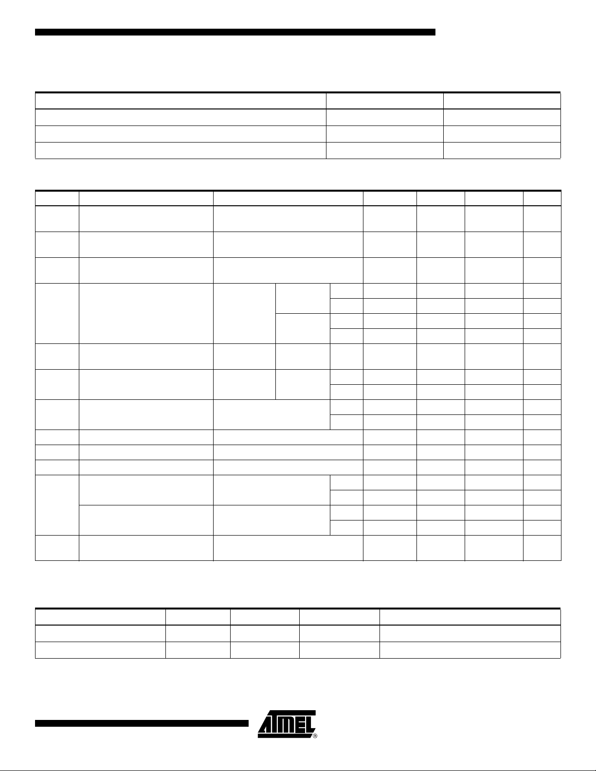
DC and AC Operating Conditions
Commercial Industrial
Operating Temperature (Ambient) 0°C - 70°C-40°C - 85°C
or V
V
CCINT
(3.3V) Power Supply 3.0V - 3.6V 3.0V - 3.6V
V
CCIO
(5V) Power Supply 5V ± 5% 5V ± 10%
CCIO
DC Characteristics
Symbol Parameter Condition Min Typ Max Units
I
IL
I
IH
I
OZ
I
CC1
I
CC2
(2)
I
CC3
V
CCIO
V
CCIO
V
IL
V
IH
V
OL
V
OH
Notes: 1. Not more than one output at a time should be shorted. Duration of short circuit test should not exceed 30 sec.
Input or I/O Low
Leakage Current
Input or I/O High
Leakage Current
Tri-state Output
Off-state Current
Power Supply Current,
Standby
Power Supply Current,
Power-down Mode
Current in Reduced-power
Mode
Supply Voltage 5.0V Device Output
V
IN
= V
CC
-2 -10 µA
210
= VCC or GND -40 40 µA
V
O
Com. 105 mA
Ind. 130 mA
Com. 10 µA
Ind. 10 µA
Com 85 ma
Ind 105
VCC = Max
V
= 0, V
IN
VCC = Max
= 0, V
V
IN
VCC = Max
= 0, VCC
V
IN
Std Mode
CC
“L” Mode
“PD” Mode 1 10 mA
CC
Std Power
Com. 4.75 5.25 V
Ind. 4.5 5.5 V
Supply Voltage 3.3V Device Output 3.0 3.6 V
Input Low Voltage -0.3 0.8 V
Input High Voltage 2.0 V
Output Low Voltage (TTL)
Output Low Voltage (CMOS)
Output High Voltage (TTL)
= VIH or V
V
IN
V
= MIN, IOL = 12 mA
CCIO
= VIH or V
V
IN
IL
IL
VCC = MIN, IOL = 0.1 mA
V
= VIH or V
IN
V
= MIN, IOH = -4.0 mA
CCIO
IL
Com. 0.45 V
Ind.
Com. .2 V
Ind. .2 V
2.4 V
+ 0.3 V
CCIO
2. When macrocell reduced-power feature is enabled.
Pin Capacitance
Typ Max Units Conditions
C
IN
C
I/O
Note: Typical values for nominal supply voltage. This parameter is only sampled and is not 100% tested.
The OGI pin (high-voltage pin during programming) has a maximum capacitance of 12 pF.
0950O–PLD–7/05
810 pF V
810 pF V
IN
OUT
= 0V; f = 1.0 MHz
= 0V; f = 1.0 MHz
11

Absolute Maximum Ratings*
Temperature Under Bias.................................. -40°C to +85°C
Storage Temperature ..................................... -65°C to +150°C
Voltage on Any Pin with
Respect to Ground .........................................-2.0V to +7.0V
Voltage on Input Pins
with Respect to Ground
During Programming.....................................-2.0V to +14.0V
Programming Voltage with
Respect to Ground .......................................-2.0V to +14.0V
AC Characteristics
-7 -10 -15 -20 -25
Symbol Parameter
*NOTICE: Stresses beyond those listed under “Absolute
Maximum Ratings” may cause permanent damage to the device. This is a stress rating only and
functional operation of the device at these or any
(1)
other conditions beyond those indicated in the
operational sections of this specification is not
implied. Exposure to absolute maximum rating
conditions for extended periods may affect device
(1)
reliability.
Note: 1. Minimum voltage is -0.6V DC, which may under-
shoot to -2.0V for pulses of less than 20 ns. Max-
(1)
imum output pin voltage is V
which may overshoot to 7.0V for pulses of less
+ 0.75V DC,
CC
than 20 ns.
UnitsMin Max Min Max Min Max Min Max Min Max
t
PD1
t
PD2
t
SU
t
H
t
FSU
t
FH
t
COP
t
CH
t
CL
t
ASU
t
AH
t
ACOP
t
ACH
t
ACL
t
CNT
f
CNT
t
ACNT
f
ACNT
Input or Feedback to
Non-registered Output
I/O Input or Feedback to
Non-registered Feedback
7.5 10 3 15 20 25 ns
793121625ns
Global Clock Setup Time 6 7 11 16 20 ns
Global Clock Hold Time 0 0 0 0 0 ns
Global Clock Setup Time of
Fast Input
Global Clock Hold Time of
Fast Input
33335ns
0.5 0.5 1.0 1.5 2 ns
Global Clock to Output Delay 4.5 5 8 10 13 ns
Global Clock High Time 3 4 5 6 7 ns
Global Clock Low Time 3 4 5 6 7 ns
Array Clock Setup Time 3 3 4 4 5 ns
Array Clock Hold Time 2 3 4 5 6 ns
Array Clock Output Delay 7.5 10 15 20 25 ns
Array Clock High Time 3 4 6 8 10 ns
Array Clock Low Time 3 4 6 8 10 ns
Minimum Clock Global Period 8 10 13 17 22 ns
Maximum Internal Global
Clock Frequency
125 100 76.9 66 50 MHz
Minimum Array Clock Period 8 10 13 17 22 ns
Maximum Internal Array
Clock Frequency
125 100 76.9 66 50 MHz
12
ATF1504AS(L)
0950O–PLD–7/05

AC Characteristics (Continued)
Symbol Parameter
ATF1504AS(L)
-7 -10 -15 -20 -25
UnitsMin Max Min Max Min Max Min Max Min Max
f
MAX
t
IN
t
IO
t
FIN
t
SEXP
t
PEXP
t
LAD
t
LAC
t
IOE
Maximum Clock Frequency 166.7 125 100 83.3 60 MHz
Input Pad and Buffer Delay 0.5 0.5 2 2 2 ns
I/O Input Pad and Buffer Delay 0.5 0.5 2 2 2 ns
Fast Input Delay 112 22ns
Foldback Term Delay 4 5 8 10 12 ns
Cascade Logic Delay 0.8 0.8 1 1 1.2 ns
Logic Array Delay 356 78ns
Logic Control Delay 356 78ns
Internal Output Enable Delay 2 2 3 3 4 ns
Output Buffer and Pad Delay
t
OD1
(Slow slew rate = OFF;
= 5V; CL = 35 pF)
V
CCIO
Output Buffer and Pad Delay
t
OD2
(Slow slew rate = OFF;
= 3.3V; CL = 35 pF)
V
CCIO
Output Buffer and Pad Delay
t
OD3
(Slow slew rate = ON;
= 5V or 3.3V; CL = 35 pF)
V
CCIO
Note: See ordering information for valid part numbers.
21.54 5 6ns
2.5 2.0 5 6 7 ns
55.58 1010ns
Timing Model
0950O–PLD–7/05
13

AC Characteristics (Continued)
Symbol Parameter
Output Buffer Enable Delay
t
t
t
t
ZX1
ZX2
ZX3
XZ
(Slow slew rate = OFF;
= 5.0V; CL = 35 pF)
V
CCIO
Output Buffer Enable Delay
(Slow slew rate = OFF;
= 3.3V; CL = 35 pF)
V
CCIO
Output Buffer Enable Delay
(Slow slew rate = ON;
= 5.0V/3.3V; CL = 35 pF)
V
CCIO
Output Buffer Disable Delay
(CL = 5 pF)
-7 -10 -15 -20 -25
UnitsMin Max Min Max Min Max Min Max Min Max
4.0 5.0 7 9 10 ns
4.5 5.5 7 9 10 ns
9 9 10 11 12 ns
45678ns
t
SU
t
H
t
FSU
t
FH
t
RD
t
COMB
t
IC
t
EN
t
GLOB
t
PRE
t
CLR
t
UIM
t
RPA
Register Setup Time 3 3 4 5 6 ns
Register Hold Time 2 3 4 5 6 ns
Register Setup Time of Fast Input 3 3 2 2 3 ns
Register Hold Time of Fast Input 0.5 0.5 2 2 2.5 ns
Register Delay 1 2 1 2 2 ns
Combinatorial Delay 1 2 1 2 2 ns
Array Clock Delay 3 5 6 7 8 ns
Register Enable Time 3 5 6 7 8 ns
Global Control Delay 1 1 1 1 1 ns
Register Preset Time 2 3 4 5 6 ns
Register Clear Time 2 3 4 5 6 ns
Switch Matrix Delay 1 1 2 2 2 ns
Reduced-power Adder
(2)
10 11 13 14 15 ns
Notes: 1. See ordering information for valid part numbers.
2. The t
parameter must be added to the t
RPA
LAD
, t
LAC,tTIC
, t
ACL
, and t
power mode.
Input Test Waveforms and Measurement Levels
parameters for macrocells running in the reduced-
SEXP
tR, tF = 1.5 ns typical
14
ATF1504AS(L)
0950O–PLD–7/05

ATF1504AS(L)
Output AC Test Loads
Note: *Numbers in parenthesis refer to 3.0V operating conditions (preliminary).
Power-down Mode The ATF1504AS includes an optional pin-controlled power-down feature. When this
mode is enabled, the PD pin acts as the power-down pin. When the PD pin is high, the
device supply current is reduced to less than 10 mA. During power-down, all output data
and internal logic states are latched internally and held. Therefore, all registered and
combinatorial output data remain valid. Any outputs that were in a high-Z state at the
onset will remain at high-Z. During power-down, all input signals except the power-down
pin are blocked. Input and I/O hold latches remain active to ensure that pins do not float
to indeterminate levels, further reducing system power. The power-down mode feature
is enabled in the logic design file or as a fitted or translated s/w option. Designs using
the power-down pin may not use the PD pin as a logic array input. However, all other PD
pin macrocell resources may still be used, including the buried feedback and foldback
product term array inputs.
Power Down AC Characteristics
Symbol Parameter
t
IVDH
t
GVDH
t
CVDH
t
DHIX
t
DHGX
t
DHCX
t
DLIV
t
DLGV
t
DLCV
t
DLOV
Notes: 1. For slow slew outputs, add t
Valid I, I/O before PD High 7 10 15 20 25 ns
Valid OE
Valid Clock
(2)
before PD High 7 10 15 20 25 ns
(2)
before PD High 7 10 15 20 25 ns
I, I/O Don’t Care after PD High 12 15 25 30 35 ns
(2)
OE
Don’t Care after PD High 12 15 25 30 35 ns
(2)
Clock
Don’t Care after PD High 12 15 25 30 35 ns
PD Low to Valid I, I/O 11111µs
PD Low to Valid OE (Pin or Term) 11111µs
PD Low to Valid Clock (Pin or Term)11111µs
PD Low to Valid Output 11111µs
.
SSO
2. Pin or product term.
3. Includes t
due to reduced power bit enabled.
RPA
(1)(2)
-7 -10 -15 -20 -25
UnitsMin Max Min Max Min Max Min Max Min Max
0950O–PLD–7/05
15

JTAG-BST/ISP Overview
The JTAG boundary-scan testing is controlled by the Test Access Port (TAP) controller
in the ATF1504AS. The boundary-scan technique involves the inclusion of a shift-register stage (contained in a boundary-scan cell) adjacent to each component so that
signals at component boundaries can be controlled and observed using scan testing
principles. Each input pin and I/O pin has its own boundary-scan cell (BSC) in order to
support boundary scan testing. The ATF1504AS does not currently include a Test Reset
(TRST) input pin because the TAP controller is automatically reset at power-up. The five
JTAG modes supported include: SAMPLE/PRELOAD, EXTEST, BYPASS, IDCODE
and HIGHZ. The ATF1504AS’s ISP can be fully described using JTAG’s BSDL as
described in IEEE Standard 1149.1b. This allows ATF1504AS programming to be
described and implemented using any one of the third-party development tools supporting this standard.
The ATF1504AS has the option of using four JTAG-standard I/O pins for boundary-scan
testing (BST) and in-system programming (ISP) purposes. The ATF1504AS is programmable through the four JTAG pins using the IEEE standard JTAG programming protocol
established by IEEE Standard 1149.1 using 5V TTL-level programming signals from the
ISP interface for in-system programming. The JTAG feature is a programmable option.
If JTAG (BST or ISP) is not needed, then the four JTAG control pins are available as I/O
pins.
JTAG Boundary-scan Cell (BSC) Testing
The ATF1504AS contains up to 68 I/O pins and four input pins, depending on the device
type and package type selected. Each input pin and I/O pin has its own boundary-scan
cell (BSC) in order to support boundary-scan testing as described in detail by IEEE
Standard 1149.1. A typical BSC consists of three capture registers or scan registers and
up to two update registers. There are two types of BSCs, one for input or I/O pin, and
one for the macrocells. The BSCs in the device are chained together through the capture registers. Input to the capture register chain is fed in from the TDI pin while the
output is directed to the TDO pin. Capture registers are used to capture active device
data signals, to shift data in and out of the device and to load data into the update registers. Control signals are generated internally by the JTAG TAP controller. The BSC
configuration for the input and I/O pins and macrocells are shown below.
BSC Configuration for Input and I/O Pins (Except JTAG TAP Pins)
Note: The ATF1504AS has pull-up option on TMS and TDI pins. This feature is selected as a design option.
16
ATF1504AS(L)
0950O–PLD–7/05

BSC Configuration for Macrocell
ATF1504AS(L)
Pin BSC
TDO
OEJ
OUTJ
Pin
TDO
0
1
0
1
DQ
DQ
0
1
TDI
Shift
DQ
DQ
Capture
Clock
DQ
DR
0
1
0
1
Pin
0950O–PLD–7/05
TDI
Shift
Capture
DR
Macrocell BSC
Update
DR
Mode
Clock
17

PCI Compliance The ATF1504AS also supports the growing need in the industry to support the new
Peripheral Component Interconnect (PCI) interface standard in PCI-based designs and
specifications. The PCI interface calls for high current drivers, which are much larger
than the traditional TTL drivers. In general, PLDs and FPGAs parallel outputs to support
the high current load required by the PCI interface. The ATF1504AS allows this without
contributing to system noise while delivering low output-to-output skew. Having a programmable high drive option is also possible without increasing output delay or pin
capacitance. The PCI electrical characteristics appear on the next page.
PCI Voltage-to-current Curves for +5V Signaling in Pull-up Mode
point
Pull Up
-44
Current (mA)
Test Point
-178
VCC
2.4
1.4
Voltage
DC
drive point
AC drive
-2
PCI Voltage-to-current Curves for +5V Signaling in Pull-down Mode
VCC
Voltage
2.2
Pull Down
AC drive
point
18
ATF1504AS(L)
0.55
DC
drive point
3,6
95
Test Point
Current (mA)
380
0950O–PLD–7/05

ATF1504AS(L)
PCI DC Characteristics
Symbol Parameter Conditions Min Max Units
V
CC
V
IH
V
IL
I
IH
I
IL
V
OH
V
OL
C
IN
C
CLK
C
IDSEL
L
PIN
Note: Leakage current is with pin-keeper off.
Supply Voltage 4.75 5.25 V
Input High Voltage 2.0 VCC + 0.5 V
Input Low Voltage -0.5 0.8 V
Input High Leakage Current VIN = 2.7V 70 µA
Input Low Leakage Current VIN = 0.5V -70 µA
Output High Voltage I
Output Low Voltage I
= -2 mA 2.4 V
OUT
= 3 mA, 6 mA 0.55 V
OUT
Input Pin Capacitance 10 pF
CLK Pin Capacitance 12 pF
IDSEL Pin Capacitance 8pF
Pin Inductance 20 nH
PCI AC Characteristics
Symbol Parameter Conditions Min Max Units
≤ 1.4 -44 mA
OUT
< 2.4 -44+(V
OUT
< V
OUT
CC
= 3.1V -142 µA
OUT
> 2.2V 95 mA
OUT
> 0 V
OUT
> 0 Equation B mA
OUT
= 0.71 206 mA
OUT
+ 2.45) for VCC > V
OUT
) for 0V < V
OUT
< 0.71V.
OUT
- 1.4)/0.024 mA
OUT
Equation A mA
/0.023 mA
OUT
+ 1)/0.015 mA
IN
> 3.1V.
OUT
Switching
I
OH(AC)
Current High
(Test High)
Switching
I
OL(AC)
Current Low
(Test Point)
I
CL
SLEW
SLEW
Low Clamp Current -5 < VIN ≤ -1 -25+(V
Output Rise Slew Rate 0.4V to 2.4V load 0.5 3 V/ns
R
Output Fall Slew Rate 2.4V to 0.4V load 0.5 3 V/ns
F
Notes: 1. Equation A: IOH = 11.9 (V
2. Equation B: I
= 78.5 * V
OL
- 5.25) * (V
OUT
* (4.4 - V
OUT
0 < V
1.4 < V
3.1 < V
V
V
2.2 > V
0.1 > V
V
0950O–PLD–7/05
19

ATF1504AS Dedicated Pinouts
44-lead
Dedicated Pin
INPUT/OE2/GCLK2 40 2 2 2 92 90
INPUT/GCLR 39 1 1 1 91 89
INPUT/OE1 384468849088
INPUT/GCLK1374367838987
I/O /GCLK3 354165818785
I/O/PD (1,2) 5, 19 11, 25 17, 37 20, 46 14, 44 12, 42
I/O/TDI (JTAG) 1 7 12 14 6 4
I/O/TMS (JTAG) 7 13 19 23 17 15
I/O/TCK (JTAG) 26 32 50 62 64 62
I/O/TDO (JTAG) 32 38 57 71 75 73
GND 4, 16, 24, 36 10, 22, 30, 42
V
CCINT
V
CCIO
N/C – – – –
TQFP
9, 17, 29, 41 3, 15, 23, 35 3, 35 3, 43 41, 93 39, 91
––
44-lead
J-lead
68-lead
J-lead
6, 16, 26, 34,
38, 48, 58, 66
11, 21, 31, 43,
53, 63
84-lead
J-lead
7, 19, 32, 42,
47, 59, 72, 82
13, 26, 38, 53,
66, 78
100-lead
PQFP
13, 28, 40, 45,
61, 76, 88, 97
5, 20, 36, 53,
68, 84
1, 2, 7, 9,
24, 26, 29, 30,
51, 52, 55, 57,
72, 74, 79, 80
100-lead
TQFP
11, 26, 38, 43,
59, 74, 86, 95
3, 18, 34, 51,
66, 82
1, 2, 5, 7, 22,
24, 27, 28, 49,
50, 53, 55, 70,
72, 77, 78
# of Signal Pins 36 36 52 68 68 68
# User I/O Pins 32 32 48 64 64 64
OE (1, 2) Global OE Pins
GCLR Global Clear Pin
GCLK (1, 2, 3) Global Clock Pins
PD (1, 2) Power down pins
TDI, TMS, TCK, TDO JTAG pins used for boundary-scan testing or in-system programming
GND Ground Pins
V
CCINT
V
CCIO
VCC pins for the device (+5V - Internal)
VCC pins for output drivers (for I/O pins) (+5V or 3.3V - I/Os)
20
ATF1504AS(L)
0950O–PLD–7/05

ATF1504AS(L)
ATF1504AS I/O Pinouts
44-
lead
MC PLC
1 A 12 6 18 22 16 14 33 C 24 18 36 44 42 40
2 A – – – 21 15 13 34 C – – – 45 43 41
3
4 A 9 3 15 18 12 10 36 C 26 20 39 48 46 44
5 A 8 2 14 17 11 9 37 C 27 21 40 49 47 45
6 A – – 13 16 10 8 38 C – – 41 50 48 46
7 A – – – 15 8 6 39 C – – – 51 49 47
8/
TDI
9 A – – 10 12 4 100 41 C 29 23 44 54 54 52
10 A – – – 11 3 99 42 C – – – 55 56 54
11 A 6 44 9 10 100 98 43 C – – 45 56 58 56
12 A – – 8 9 99 97 44 C – – 46 57 59 57
13 A – – 7 8 98 96 45 C – – 47 58 60 58
14 A 5 43 5 6 96 94 46 C 31 25 49 60 62 60
15A–––5959347C –––616361
16 A 4 42 4 4 94 92
17 B 21 15 33 41 39 37 49 D 33 27 51 63 65 63
18 B – – – 40 38 36 50 D – – – 64 66 64
19 B 20 14 32 39 37 35 51 D 34 28 52 65 67 65
20 B 19 13 30 37 35 33 52 D 36 30 54 67 69 67
21 B 18 12 29 36 34 32 53 D 37 31 55 68 70 68
22 B – – 28 35 33 31 54 D – – 56 69 71 69
23 B – – – 34 32 30 55 D – – – 70 73 71
24B17112733 31 29
25 B 16 10 25 31 27 25 57 D 39 33 59 73 77 75
26 B – – – 30 25 23 58 D – – – 74 78 76
27 B – – 24 29 23 21 59 D – – 60 75 81 79
28 B – – 23 28 22 20 60 D – – 61 76 82 80
29 B – – 22 27 21 19 61 D – – 62 77 83 81
30 B 14 8 20 25 19 17 62 D 40 34 64 79 85 83
31 B – – – 24 18 16 63 D – – – 80 86 84
32/
TMS
PLCC
A/
PD1
A 7 1 12 14 6 4 40 C 28 22 42 52 50 48
B 13 7 19 23 17 15 64
44-
lead
TQFP
11 5 17 20 14 12 35
68-
lead
PLCC
84-
lead
PLCC
100-
lead
PQFP
100-
lead
TQFP MC PLC
48/
TCK
56/
TDO
44-
lead
PLCC
C/
PD2
C 32265062 64 62
D 38325771 75 73
D/
GCLK3
44-
lead
TQFP
25 19 37 46 44 42
41 35 65 81 87 85
68-
lead
PLCC
84-
lead
PLCC
100-
lead
PQFP
100-
lead
TQFP
0950O–PLD–7/05
21

SUPPLY CURRENT VS. SUPPLY VOLTAGE
= 25°C, F = 0)
(T
125
100
75
(mA)
CC
I
50
25
0
4.50 4.75 5.00 5.25 5.50
A
STANDARD
REDUCED POWER MODE
(V)
V
CC
SUPPLY CURRENT VS. SUPPLY VOLTAGE
PIN-CONTROLLED POWER-DOWN MODE
(T
= 25°C, F = 0)
1100
1000
900
(µA)
CC
I
800
700
4.50 4.75 5.00 5.25 5.50
A
STANDARD POWER
REDUCED POWER MODE
(V)
V
CC
SUPPLY CURRENT VS. SUPPLY VOLTAGE
LOW-POWER ("L") VERSION
= 25°C, F = 0)
(T
A
30
20
(µA)
CC
I
10
0
4.50 4.75 5.00 5.25 5.50
VCC (V)
SUPPLY CURRENT VS. FREQUENCY
200.0
STANDARD POWER (T
150.0
100.0
(mA)
CC
I
50.0
0.0
STANDARD POWER
0.00 20.00 40.00 60.00 80.00 100.00
FREQUENCY (MHz)
= 25°C)
A
REDUCED POWER MODE
SUPPLY CURRENT VS. FREQUENCY
LOW-POWER ("L") VERSION
125.0
LOW POWER (T
100.0
75.0
(mA)
CC
I
50.0
25.0
0.0
0.00 5.00 10.00 15.00 20.00 25.00
STANDARD POWER
FREQUENCY (MHz)
= 25°C)
A
REDUCED POWER MODE
OUTPUT SOURCE CURRENT VS. OUTPUT VOLTAGE
(V
= 5V, TA = 25°C)
0.0
-10.0
-20.0
-30.0
-40.0
-50.0
IOH (mA)
-60.0
-70.0
-80.0
-90.0
-100.0
0.00 0.50 1.00 1.50 2.00 2.50 3.00 3.50 4.00 4.50 5.00
CC
OUTPUT VOLTAGE (V)
22
OUTPUT SOURCE CURRENT VS. SUPPLY VOLTAGE
0.0
-10.0
-20.0
-30.0
IOH (mA)
-40.0
-50.0
-60.0
4.50 4.75 5.00 5.25 5.50
(VOH = 2.4V, T
SUPPLY VOLTAGE (V)
= 25°C)
A
ATF1504AS(L)
INPUT CLAMP CURRENT VS. INPUT VOLTAGE
= 5V, TA = 25°C)
(V
0
-10
-20
-30
-40
INPUT CURRENT (mA)
-50
-60
-1.00 -0.80 -0.60 -0.40 -0.20 0.00
CC
INPUT VOLTAGE (V)
0950O–PLD–7/05

ATF1504AS(L)
OUTPUT SINK CURRENT VS. SUPPLY VOLTAGE
43
42
41
40
39
38
IOL (mA)
37
36
35
34
4.50 4.75 5.00 5.25 5.50
(VOL = 0.5V, T
SUPPLY VOLTAGE (V)
= 25°C)
A
NORMALIZED TPD
1.20
VS. SUPPLY VOLTAGE (T
1.10
1.00
NORMALIZED TPD
0.90
0.80
4.5 4.8 5.0 5.3 5.5
SUPPLY VOLTAGE (V)
= 25°C)
A
NORMALIZED TPD
VS. TEMPERATURE (V
1.2
1.1
1.0
NORMALIZED TPD
0.9
0.8
-40.0 0.0 25.0 75.0
TEMPERATURE (C)
NORMALIZED TCO
1.2
1.1
1.0
NORMALIZED TPD
0.9
VS. SUPPLY VOLTAGE (T
= 5.0V)
CC
= 25°C)
A
INPUT CURRENT VS. INPUT VOLTAGE
= 5V, TA = 25°C)
(V
40
30
20
10
0
-10
INPUT CURRENT ( A)
-20
-30
0.0 0.5 1.0 1.5 2.0 2.5 3.0 3.5 4.0 4.5 5.0
CC
INPUT VOLTAGE (V)
OUTPUT SINK CURRENT VS. OUTPUT VOLTAGE
(V
= 5V, TA = 25°C)
140.0
120.0
100.0
80.0
60.0
IOL (mA)
40.0
20.0
0.0
0.00 0.50 1.00 1.50 2.00 2.50 3.00 3.50 4.00 4.50 5.00
CC
OUTPUT VOLTAGE (V)
0.8
4.5 4.8 5.0 5.3 5.5
SUPPLY VOLTAGE (V)
NORMALIZED TSU
1.2
1.1
1.0
NORMALIZED TSU
0.9
0.8
VS. SUPPLY VOLTAGE (T
4.5 4.8 5.0 5.3 5.5
SUPPLY VOLTAGE (V)
= 25°C)
A
0950O–PLD–7/05
23

NORMALIZED TCO
1.2
1.1
1.0
NORMALIZED TCO
0.9
0.8
-40.0 0.0 25.0 75.0
VS.TEMPERATURE (V
TEMPERATURE (C)
= 5.0V)
CC
NORMALIZED TSU
1.2
VS. TEMPERATURE (V
1.1
1.0
NORMALIZED TSU
0.9
0.8
-40.0 0.0 25. 0 75.0
TEMPERATURE (C)
= 5.0V)
CC
24
ATF1504AS(L)
0950O–PLD–7/05

Ordering Information
ATF1504AS Standard Package Options
t
PD
(ns)
7.5 4.5 166.7
10 5 125
10 5 125
15 8 100
15 8 100
Notes: 1. The last time buy date is Sept. 30, 2005 for shaded parts.
t
CO1
(ns)
2. For the QC100 package, customers may migrate to the ATF1508AS-10QU100 or AU100.
f
MAX
(MHz) Ordering Code Package Operation Range
ATF1504AS-7 AC44
ATF1504AS-7 JC44
ATF1504AS-7 JC68
ATF1504AS-7 JC84
ATF1504AS-7 QC100
ATF1504AS-7 AC100
ATF1504AS-10 AC44 44A
ATF1504AS-10 JC44 44J
ATF1504AS-10 JC68 68J
ATF1504AS-10 JC84 84J
ATF1504AS-10 QC100 100Q1
ATF1504AS-10 AC100 100A
ATF1504AS-10 AI44
ATF1504AS-10 JI44
ATF1504AS-10 JI68
ATF1504AS-10 JI84
ATF1504AS-10 QI100
ATF1504AS-10 AI100
ATF1504AS-15 AC44
ATF1504AS-15 JC44
ATF1504AS-15 JC68 68J
ATF1504AS-15 JC84 84J
ATF1504AS-15 QC100 100Q1
ATF1500AS-15 AC100 100A
ATF1504AS-15 AI44
ATF1504AS-15 JI44
ATF1504AS-15 JI68
ATF1504AS-15 JI84
ATF1504AS-15 QI100
ATF1504AS-15 AI100
44A
44J
68J
84J
100Q1
100A
44A
44J
68J
84J
100Q1
100A
44A
44J
44A
44J
68J
84J
100Q1
100A
ATF1504AS(L)
Commercial
(0°C to 70°C)
Commercial
(0°C to 70°C)
Industrial
(-40°C to +85°C)
Commercial
(0°C to 70°C)
Industrial
(-40°C to +85°C)
Using “C” Product for Industrial
To use commercial product for Industrial temperature ranges, down-grade one speed grade from the “I” to the “C” device
(7 ns “C” = 10 ns “I”) and de-rate power by 30%.
25
0950O–PLD–7/05

ATF1504AS Green Package Options (Pb/Halide-free/RoHS Compliant)
t
PD
(ns)
7.5 4.5 166.7
10 5 125
t
CO1
(ns)
f
MAX
(MHz) Ordering Code Package Operation Range
ATF1504AS-7 AX44
ATF1504AS-7 JX44
ATF1504AS-10 AU44 44A
ATF1504AS-10 JU44 44J
ATF1504AS-10AU100 100A
ATF1504AS-10 JU84 84J
44A
44J
Commercial
(0°C to 70°C)
Industrial
(-40°C to +85°C)
Package Type
44A 44-lead, Thin Plastic Gull Wing Quad Flatpack (TQFP)
44J 44-lead, Plastic J-leaded Chip Carrier (PLCC)
68J 68-lead, Plastic J-leaded Chip Carrier (PLCC)
84J 84-lead, Plastic J-leaded Chip Carrier (PLCC)
100Q1 100-lead, 14 x 20 mm Body, Plastic Quad Flat Package (PQFP)
100A 100-lead, 14 x 14 mm Body, Thin Profile Plastic Quad Flat Package (TQFP)
26
ATF1504AS(L)
0950O–PLD–7/05

ATF1504ASL Standard Package Options
t
PD
(ns)
20 12 83.3
25 15 70
Note: 1. The last time buy date is Sept. 30, 2005 for shaded parts.
t
CO1
(ns)
f
MAX
(MHz) Ordering Code Package Operation Range
ATF1504ASL-20 AC44
ATF1504ASL-20 JC44
ATF1504ASL-20 JC68
ATF1504ASL-20 JC84
ATF1504ASL-20 QC100
ATF1504ASL-20 AC100
ATF1504ASL-25 AI44
ATF1504ASL-25 JI84
ATF1504ASL-25 JI68
ATF1504ASL-25 JI84
ATF1504ASL-25 QI100
ATF1504ASL-25 AI100
44A
44J
68J
84J
100Q1
100A
44A
44J
68J
84J
100Q1
100A
ATF1504AS(L)
Commercial
(0°C to 70°C)
Industrial
(-40°C to +85°C)
Using “C” Product for Industrial
To use commercial product for Industrial temperature ranges, down-grade one speed grade from the “I” to the “C” device
(7 ns “C” = 10 ns “I”) and de-rate power by 30%.
ATF1504ASL Green Package Options (Pb/Halide-free/RoHS Compliant)
t
PD
(ns)
25 15 70
44A 44-lead, Thin Plastic Gull Wing Quad Flatpack (TQFP)
t
CO1
(ns)
f
MAX
(MHz) Ordering Code Package Operation Range
ATF1504ASL-25 AU44
ATF1504ASL-25 JU44
ATF1504ASL-25 AU100
Package Type
44A
44J
100A
Industrial
(-40°C to +85°C)
44J 44-lead, Plastic J-leaded Chip Carrier (PLCC)
68J 68-lead, Plastic J-leaded Chip Carrier (PLCC)
84J 84-lead, Plastic J-leaded Chip Carrier (PLCC)
100Q1 100-lead, 14 x 20 mm Body, Plastic Quad Flat Package (PQFP)
100A 100-lead, 14 x 14 mm Body, Thin Profile Plastic Quad Flat Package (TQFP)
0950O–PLD–7/05
27

Packaging Information
44A – TQFP
PIN 1
B
PIN 1 IDENTIFIER
e
E1 E
D1
D
C
0˚~7˚
A1
L
Notes: 1. This package conforms to JEDEC reference MS-026, Variation ACB.
2. Dimensions D1 and E1 do not include mold protrusion. Allowable
protrusion is 0.25 mm per side. Dimensions D1 and E1 are maximum
plastic body size dimensions including mold mismatch.
3. Lead coplanarity is 0.10 mm maximum.
A2 A
SYMBOL
COMMON DIMENSIONS
(Unit of Measure = mm)
MIN
A – – 1.20
A1 0.05 – 0.15
A2 0.95 1.00 1.05
D 11.75 12.00 12.25
D1 9.90 10.00 10.10 Note 2
E 11.75 12.00 12.25
E1 9.90 10.00 10.10 Note 2
B 0.30 – 0.45
C 0.09 – 0.20
L 0.45 – 0.75
e 0.80 TYP
NOM
MAX
NOTE
28
2325 Orchard Parkway
TITLE
R
San Jose, CA 95131
ATF1504AS(L)
44A, 44-lead, 10 x 10 mm Body Size, 1.0 mm Body Thickness,
0.8 mm Lead Pitch, Thin Profile Plastic Quad Flat Package (TQFP)
10/5/2001
DRAWING NO.
44A
0950O–PLD–7/05
REV.
B

44J – PLCC
ATF1504AS(L)
1.14(0.045) X 45˚
B
e
0.51(0.020)MAX
45˚ MAX (3X)
Notes: 1. This package conforms to JEDEC reference MS-018, Variation AC.
2. Dimensions D1 and E1 do not include mold protrusion.
Allowable protrusion is .010"(0.254 mm) per side. Dimension D1
and E1 include mold mismatch and are measured at the extreme
material condition at the upper or lower parting line.
3. Lead coplanarity is 0.004" (0.102 mm) maximum.
PIN NO. 1
IDENTIFIER
D1
D
1.14(0.045) X 45˚
E1 E
0.318(0.0125)
0.191(0.0075)
NOM
D2/E2
MAX
B1
A2
A1
A
COMMON DIMENSIONS
(Unit of Measure = mm)
SYMBOL
A 4.191 – 4.572
A1 2.286 – 3.048
A2 0.508 – –
D 17.399 – 17.653
D1 16.510 – 16.662 Note 2
E 17.399 – 17.653
E1 16.510 – 16.662 Note 2
D2/E2 14.986 – 16.002
B 0.660 – 0.813
B1 0.330 – 0.533
e 1.270 TYP
MIN
NOTE
R
0950O–PLD–7/05
2325 Orchard Parkway
San Jose, CA 95131
TITLE
44J, 44-lead, Plastic J-leaded Chip Carrier (PLCC)
DRAWING NO.
44J
10/04/01
REV.
B
29

68J – PLCC
1.14(0.045) X 45˚
B
e
0.51(0.020)MAX
45˚ MAX (3X)
Notes: 1. This package conforms to JEDEC reference MS-018, Variation AE.
2. Dimensions D1 and E1 do not include mold protrusion.
Allowable protrusion is .010"(0.254 mm) per side. Dimension D1
and E1 include mold mismatch and are measured at the extreme
material condition at the upper or lower parting line.
3. Lead coplanarity is 0.004" (0.102 mm) maximum.
PIN NO. 1
IDENTIFIER
D1
D
1.14(0.045) X 45˚
E1 E
0.318(0.0125)
0.191(0.0075)
NOM
D2/E2
MAX
B1
A2
A1
A
COMMON DIMENSIONS
(Unit of Measure = mm)
SYMBOL
A 4.191 – 4.572
A1 2.286 – 3.048
A2 0.508 – –
D 25.019 – 25.273
D1 24.130 – 24.333 Note 2
E 25.019 – 25.273
E1 24.130 – 24.333 Note 2
D2/E2 22.606 – 23.622
B 0.660 – 0.813
B1 0.330 – 0.533
e 1.270 TYP
MIN
NOTE
30
2325 Orchard Parkway
TITLE
R
San Jose, CA 95131
ATF1504AS(L)
68J, 68-lead, Plastic J-leaded Chip Carrier (PLCC)
DRAWING NO.
68J
0950O–PLD–7/05
10/04/01
REV.
B

84J – PLCC
ATF1504AS(L)
1.14(0.045) X 45˚
B
e
0.51(0.020)MAX
45˚ MAX (3X)
Notes: 1. This package conforms to JEDEC reference MS-018, Variation AF.
2. Dimensions D1 and E1 do not include mold protrusion.
Allowable protrusion is .010"(0.254 mm) per side. Dimension D1
and E1 include mold mismatch and are measured at the extreme
material condition at the upper or lower parting line.
3. Lead coplanarity is 0.004" (0.102 mm) maximum.
PIN NO. 1
IDENTIFIER
D1
D
1.14(0.045) X 45˚
E1 E
0.318(0.0125)
0.191(0.0075)
NOM
D2/E2
MAX
B1
A2
A1
A
COMMON DIMENSIONS
(Unit of Measure = mm)
SYMBOL
A 4.191 – 4.572
A1 2.286 – 3.048
A2 0.508 – –
D 30.099 – 30.353
D1 29.210 – 29.413 Note 2
E 30.099 – 30.353
E1 29.210 – 29.413 Note 2
D2/E2 27.686 – 28.702
B 0.660 – 0.813
B1 0.330 – 0.533
e 1.270 TYP
MIN
NOTE
R
0950O–PLD–7/05
2325 Orchard Parkway
San Jose, CA 95131
TITLE
84J, 84-lead, Plastic J-leaded Chip Carrier (PLCC)
DRAWING NO.
84J
10/04/01
REV.
B
31

100Q1 – PQFP
C
PIN 1 ID
PIN 1
e
B
0º~7º
E1
E
D1
D
COMMON DIMENSIONS
A
SYMBOL
L
A1
A – 3.04 3.4
A1 0.25 0.33 0.5
D 23.20 BSC
E 17.20 BSC
E1 14.00 BSC
B 0.22 – 0.40
C 0.11 – 0.23
D1 20 BSC
L 0.73 – 1.03
e 0.65 BSC
(Unit of Measure = mm)
JEDEC STANDARD MS-022, GC-1
MIN
NOM
MAX
NOTE
32
2325 Orchard Parkway
R
San Jose, CA 95131
100Q1, 100-lead, 14 x 20 mm Body, 3.2 mm Footprint, 0.65 mm Pitch,
Plastic Quad Flat Package (PQFP)
ATF1504AS(L)
TITLE
07/6/2005
DRAWING NO.
100Q1
0950O–PLD–7/05
REV.
C

100A – TQFP
ATF1504AS(L)
PIN 1
B
PIN 1 IDENTIFIER
e
E1 E
D1
D
C
0˚~7˚
A1
L
Notes: 1. This package conforms to JEDEC reference MS-026, Variation AED.
2. Dimensions D1 and E1 do not include mold protrusion. Allowable
protrusion is 0.25 mm per side. Dimensions D1 and E1 are maximum
plastic body size dimensions including mold mismatch.
3. Lead coplanarity is 0.08 mm maximum.
A2 A
SYMBOL
COMMON DIMENSIONS
(Unit of Measure = mm)
MIN
A – – 1.20
A1 0.05 – 0.15
A2 0.95 1.00 1.05
D 15.75 16.00 16.25
D1 13.90 14.00 14.10 Note 2
E 15.75 16.00 16.25
E1 13.90 14.00 14.10 Note 2
B 0.17 – 0.27
C 0.09 – 0.20
L 0.45 – 0.75
e 0.50 TYP
NOM
MAX
NOTE
R
0950O–PLD–7/05
2325 Orchard Parkway
San Jose, CA 95131
TITLE
100A, 100-lead, 14 x 14 mm Body Size, 1.0 mm Body Thickness,
0.5 mm Lead Pitch, Thin Profile Plastic Quad Flat Package (TQFP)
10/5/2001
DRAWING NO.
100A
REV.
C
33

Revision History
Revision Comments
0950O
Green package options added.
34
ATF1504AS(L)
0950O–PLD–7/05
 Loading...