

Page 1

查询ATF1502ASV供应商
Features
• High-density, High-performance, Ele ctr ically-erasable Complex Programm able
Logic Device
– 3.0 to 3.6V Operati ng Range
– 32 Macrocells
– 5 Product Terms per Macrocell, Expandable up to 40 per Macr ocell
–44 Pins
– 15 ns Maximum Pin-to-pin Delay
– Registered Operation up to 77 MHz
– Enhanced Routing Resources
• In-System Progr am ma bility (ISP) via JTAG
• Flexible Logic Macrocell
– D/T Latch Configurable Flip-flops
– Global and Individual Register Control Signals
– Global and Individual Output Enable
– Programmable Output Slew Rate
– Programmable Output Open Collector Option
– Maximum Logic Utilization by Burying a Register with a COM Output
• Advanced Power Management Feat ures
– Pin-contr oll ed 0.75 mA Standby Mode
– Programmable Pin-keeper Inputs and I/Os
– Reduced-power Feature per Macrocell
• Avai lable in Commercial and Industrial Temperature Ranges
• Av ailable in 44-lead PLCC and TQFP
• Advanced EEPROM Technology
– 100 % Test ed
– Completely Reprogrammable
– 10,000 Program/Erase Cycles
– 20-year Data Retention
– 2000V ESD Protection
– 200 mA Latch-up Immun ity
• JTAG Boundary-scan Testing to IEEE Std. 1149.1-1990 and 1149.1a-1993 Supported
• PCI-compliant
• Security Fuse Feature
Highperformance
EEPROM CPLD
ATF1502ASV
Enhanced Features
• Improved Connectivity (Additional Feedback Routing, Alternate Input Routing)
• Output Enable Product Terms
• D Latch Mode
• Combinatorial Output with Registered Feedback within Any Macrocell
• Three Global Clock Pins
• Fast Registered Input from Product Term
• Programmable “Pin-keeper” Option
• V
Power-up Reset Option
CC
• Pull-up Option on JTAG Pins TMS and TDI
• Advanced Power Management Feat ures
– Individual Macrocell Power Option
Rev. 1615H–PLD–2/04
1
Page 2
I/O/TDI
GND
PD1/I/O
TMS/I/O
VCC
I/O
I/O
I/O
I/O
I/O
I/O
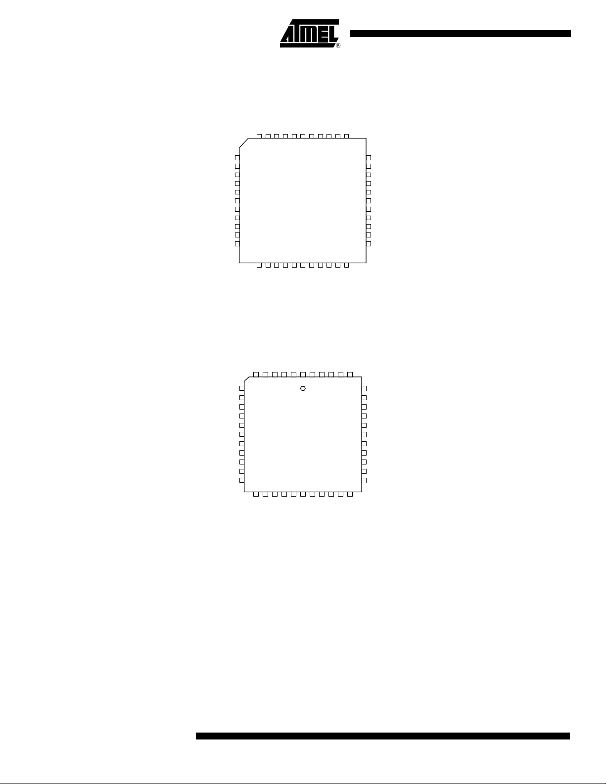
44-lead TQFP
Top View
I/O
I/O
I/O
VCC
GCLK2/OE2/I
GCLR/I
4443424140393837363534
1
2
3
4
5
6
7
8
9
10
11
1213141516171819202122
I/O
I/O
I/O
I/O
VCC
GND
44-lead PLCC
Top View
I/OE1
I/O
GCLK1/I
GND
I/O
PD2/I/O
GCLK3/I/O
I/O
33
32
31
30
29
28
27
26
25
24
23
I/O
I/O
I/O
I/O/TDO
I/O
I/O
VCC
I/O
I/O
I/O/TCK
I/O
GND
I/O
I/O
I/O
I/O
VCC
GCLK2/OE2/I
GCLR/I
OE1/I
GCLK1/I
GND
GCLK3/I/O
I/O
TDI/I/O
I/O
I/O
GND
PD1/I/O
I/O
I/O/TMS
I/O
VCC
I/O
I/O
65432
7
8
9
10
11
12
13
14
15
16
17
1819202122232425262728
I/O
I/O
I/O
I/O
GND
1
VCC
4443424140
I/O
I/O
I/O
PD2/I/O
39
38
37
36
35
34
33
32
31
30
29
I/O
I/O
I/O/TDO
I/O
I/O
VCC
I/O
I/O
I/O/TCK
I/O
GND
I/O
Description The ATF1502ASV is a high-performance, high-density complex programmable logic
device (CPLD) that utilizes A tmel’s proven electrically-erasable technology. With 32
logic macrocells and up to 36 inputs, it easily integrates logic from several TTL, SSI,
MSI, LSI and classic PLDs. The ATF1502ASV’s e nhanced routing switch matrices
increase usable gate count and the odds of successful pin-locked design modificat ions.
The ATF1502ASV has up to 32 bi-directional I/O pins and four dedicated input pins,
depending o n the t ype of d evice pac kage se lected . Eac h dedica ted pi n can also se rve
as a global co ntrol signa l, registe r clock, regi ster reset or output enable . Each of the se
control signals can be selected for use individually within each macrocell.
2
ATF1502ASV
1615H–PLD–2/04
Page 3
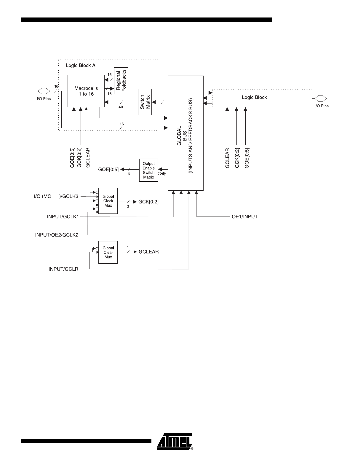
Block Diagram
ATF1502ASV
B
32
Each of the 32 macrocells generates a buried feedback that goes to t he global bus.
Each input and I/O pin also feeds into the global bus. The switch matrix in each logic
block then selects 40 individual signals f rom the glob al bus. Each m acroc ell also generates a foldb ack logic term that goes to a regional bus . Cascade log ic between
macrocells in the ATF1502ASV allows fast, efficient generation of complex logic functions. The ATF1502ASV contains four such logic chains, each capable of creating sum
term logic with a fan-in of up to 40 product terms.
The ATF1502ASV macroc ell, shown in Figure 1, is flexible enough to support highly
complex logic functions operating at high speed. The macrocell consists of five sections:
product terms and product term select multiplexer, OR/XOR/CASCADE logic, a flip-flop,
output select and enable, and logic array inputs.
1615H–PLD–2/04
Unused product t erms are automatically disabled by the compiler to decrease power
consum ption. A se curity fus e, when pro grammed , protects the conten ts of the
ATF1502ASV. Two bytes (16 bits) of User Signature are accessible to the user for purposes such as storing project name, part number, revision or date. The User Signat ure
is accessible regardless of the state of the security fuse.
The ATF1502ASV device is an in-system programmab le ( ISP) device. It uses the industry standard 4-pin JTAG interface (IEEE Std. 1149.1), and is fully compliant with JTAG’s
3
Page 4
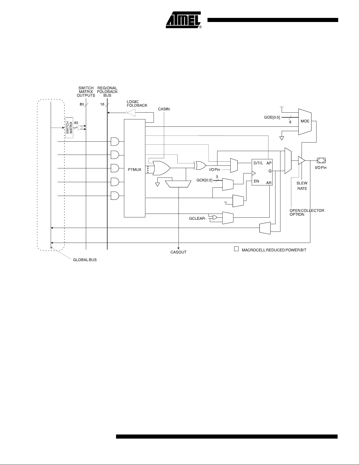
Figure 1. ATF1502A SV Ma crocel l
Boundary-scan Description Language (BSDL). ISP allows the device to be programmed
without removing it from the printed circuit board. In addition to simplifying the manufacturing flow, ISP also allows design modifications to be made in the field via software.
Product Terms and
Select Mux
OR/XOR/
CASCADE Logic
4
ATF1502ASV
Each ATF1502ASV macrocell has five product terms. Each product term receives as its
inputs all signals from both the global bus and regional bus.
The product term select multiplexer (PTMUX) allocates the five product term s as
needed to the macrocell logic gates and control signals. The PTMUX programming is
determined by the design compiler, which selects the optimum macrocell configuration.
The ATF15 02ASV’s lo gic structur e is design ed to effici ently suppo rt all types of logic.
Within a single macrocell, all the product terms can be routed to the OR gate, creating a
5-input AND/OR sum term. With the addition of the CASIN from neighboring macrocells,
this can be expanded to as many as 40 product terms with little additional delay.
The macrocell’s XOR gate allows efficient implementation of compare and arithmetic
functions. One input to the XOR comes from the OR sum term. The other XOR input can
be a product term or a fixed high or low level. For combin atorial outputs, the fixed le vel
input allows polarity selection. For registered functions, the fixed levels allow DeMorgan
minimization of product terms. The XOR gate is also used to emulate T- and JK-type
flip-flops.
1615H–PLD–2/04
Page 5

ATF1502ASV
Flip-flop The ATF1502A SV’s flip-flop h as very flexibl e data and control func tions. The dat a input
can com e fro m eit her the X OR gate , from a sepa ra te produ ct t erm o r directl y from the
I/O pin. Selecting the separat e product term allows creation of a buried registered feedback within a combinatorial output macrocell. (This feature is automatically implemented
by the fitter software). In a ddition to D, T, JK and SR operation, the flip-flop can also be
configured as a flow-through latch. In this m ode, da ta p asse s throug h when the clock is
high and is latched when the clock is low.
The clock itself can be either one of the Global CLK signals (GCK[0 : 2]) or an individual
product term. The flip-flop changes state on t he clock’s rising edge. When the GCK signal is used as the clock, one of the macrocell product terms can be selected as a clock
enable. When the clock enable function is active and the enable signa l (product term) is
low, all clock edges a re igno red. T he flip-fl op’s asy nchrono us re set sign al (AR ) can be
either the Global Clear (GCLEAR), a product term, or always off. AR can also be a l ogic
OR of G CLE AR with a p rodu ct ter m. The asy nchro no us pre se t (AP) can be a pr oduc t
term or always off.
Extra Feedback The ATF1502ASV mac rocell output can be selected as registered or combinatorial.The
extra burie d fee dback signa l can be eith er com binato rial or a regist ered s ign al rega rdless of whether the output is combinatorial or registered. (This enhancement function is
automatically implemented by the fitter software.) Feedback of a buried combinatorial
output allows the creation of a second latch within a macrocell.
I/O Control The output enable multiplexer (MOE) controls the output enable signal. Each I/O can be
individually configured as an input, output or for bi-directional operation. The output
enable for each macrocell can be selected from the true or compliment of the two output
enable pins, a subset of the I/O pins, or a subs et of the I /O macr ocell s. This se lection is
automatically done by the fitter software when the I/O is configured as an input, all macrocell resources are still available, including the buried feedback, expander and cascade
logic.
Global Bus/Switch Matrix The global bus cont ains all input and I/O p in sign als as wel l as t he buried feedback sig-
nal from all 32 macrocells. The switch matrix in each logic block receives as its inputs all
signals from the global bus. Under software control, up to 40 of these signals can be
selected as inputs to the logic block.
Foldback Bus Each macrocell also generates a foldback product term. This signal goes to the regional
bus and is availa ble to four m ac roc ells. T he foldback is an inverse pola rity of on e of the
macrocell’s product terms. The four foldback terms in each region allow generation of
high fan-in sum terms (up to nine product terms) with little additional delay.
Prog rammable Pinkeeper Option for
Inputs and I/Os
The ATF1502ASV offers the option of programming all input and I/O pins so that pinkeeper circuits can be utilized. When any pin is driven high or low and then subsequently left float ing, it will stay at t hat previous high or low le vel. This circui try prev ents
unused input and I/O lines from floating to intermediate voltage levels, whic h causes
unnecessary power consumption and system noise. The keeper c ircuits eliminate the
need for external pull-up resistors and eliminate their DC power consumption.
1615H–PLD–2/04
5
Page 6
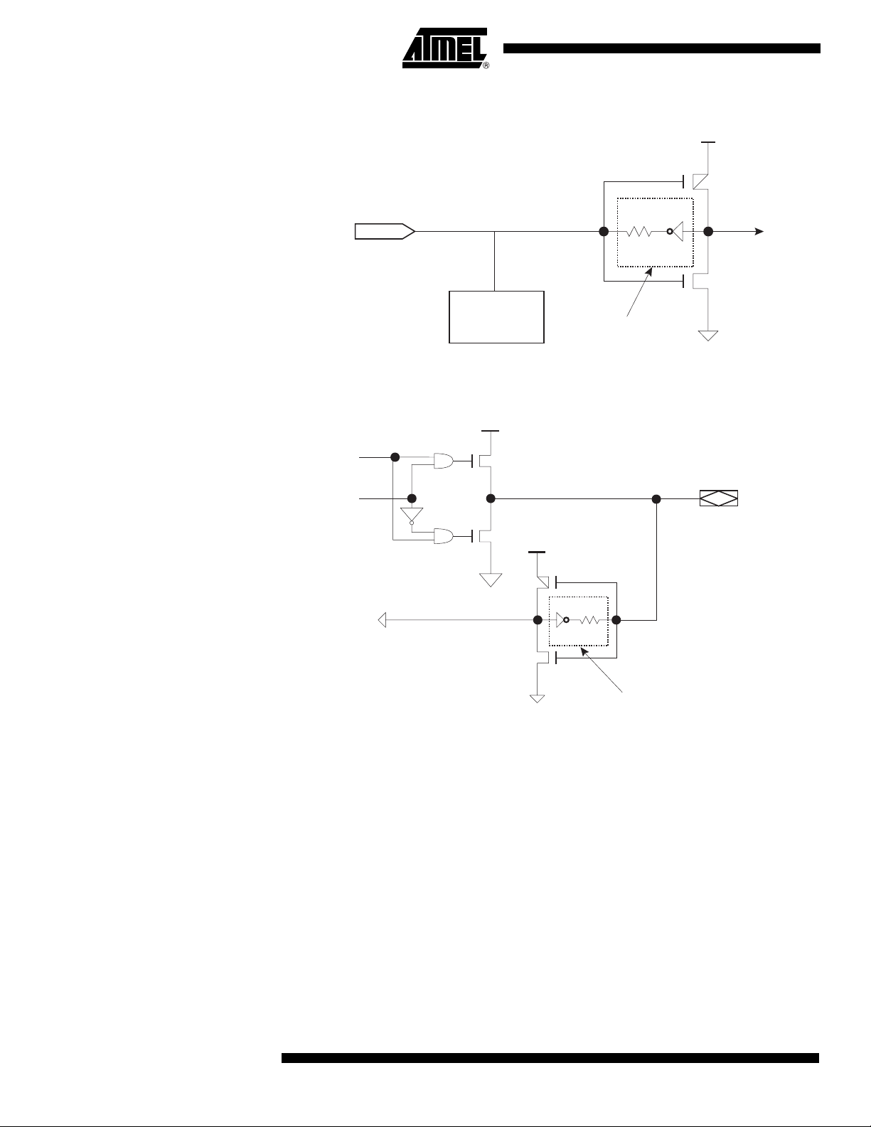
Input Diagram
V
CC
I/O Diagram
INPUT
DATA
OE
ESD
PROTECTION
CIRCUIT
V
CC
100K
PROGRAMMABLE
OPTION
I/O
V
CC
100K
Speed/Power
Management
6
ATF1502ASV
PROGRAMMABLE
OPTION
The ATF1502ASV has several built-in speed and power managem ent features.
To further reduce power, each ATF1502ASV macrocell has a reduced-power bit feature.
To reduce power consumption this feature may be actived (by changing the default
value of OFF to ON) for any or all macrocells.
The ATF1502ASV also has an optional power-down mode. In this mode, current drops
to belo w 15 m A. Wh en t he pow er- down o pti on is se lect ed, e ither PD 1 o r PD2 pins ( or
both) can be used to power down the part. The power-down option is selected in the
design source file. When enabled, the device goes into power-down when either PD1 or
PD2 is high. In the power-down mode, all internal logic signals are latched and held, as
are any enabled outputs.
All pin transitions are ignored until the PD pin is brought low. When the power-down feature is enabled, the PD1 or PD2 pin cannot be used as a logic input or output. However,
the pin’s macrocell m ay still be used to generate buried foldback and cascade logic
signals.
1615H–PLD–2/04
Page 7

ATF1502ASV
All powe r-d own AC cha rac teristi c pa ramet ers a re co mp uted f rom exte rnal inpu t or I /O
pins, with reduced-power bit turned on. For macrocells in reduced-power mode
(reduced-power bit turned on), the reduced-power adder, t
parameters, which include the data paths t
LAD
, t
LAC
, tIC, t
The ATF1502ASV mac rocell also has an option whereby the po wer can be reduced on
a per-macrocell basis. By enabling this power-down option, macrocells that are not used
in an application can be turned down, thereby reducing the ov erall power cons umptio n
of the device.
Each ou tput a ls o has i ndiv idua l slew ra te cont rol. T his m ay be us ed to redu ce s ystem
noise by slowing down outputs that do not ne ed to op erate at max imum speed. Outputs
default to slow switching, and may be specified as fast switching in the design file.
, must be added to the AC
RPA
, t
ACL
ACH
and t
SEXP
.
Design Software
Support
ATF1502ASV designs are supported by several third-party tools. Automated fitters allow
logic synthesis using a variety of high-level description languages and formats.
Power-up Reset The ATF1502ASV is designed with a power-up reset, a feature critical for state machine
initi aliz atio n. At a p oin t d ela yed sli gh tly fr om V
tialized, an d the stat e of eac h outpu t will dep end on t he pol arity o f its buffer. However,
due to the asynchronous nature of reset and uncertainty of how V
system, the following conditions are required:
1. The V
rise must be monotonic,
CC
2. After reset occurs, all input and feedback setup times must be met before
driving the clock pin high, and,
3. The clock must remain stable during T
The ATF1502ASV has two options for th e hysteresis about the reset level, V
and Large. To ensure a robus t operat ing enviro nment in applicatio ns whe re the devic e
is operated near 3.0V, Atmel recommends that during the fitting process users configure
the device with the Power-up Reset hysteresis set to Large. For conversions, Atmel
POF2JED users should include the flag “-power_reset” on th e command line after “filename.POF”. To allow the reg isters to be properly rei nitialized with the La rge hysteresis
option selected, the following condition is added:
4. If V
falls below 2.0V, it mu st shut off completely before the device is turned
CC
on again.
When the Large hysteresis option is active, I
amps as well.
crossing V
CC
.
D
is reduced by several hundred micro-
CC
, all reg is ter s wi ll be in i-
RST
actually rises in the
CC
RST
, Small
Security Fuse Usage A single fuse is provided to prevent unauthorized copying of the ATF150 2ASV fuse pat-
terns. Onc e programmed, fuse verify is inhibited. However, the 16-bit User Signature
remains accessible.
Programming ATF1502ASV devices are in-system programmable (ISP) devices utilizing the 4-pin
JTAG protocol. This capability eliminates package handling normally required for programming and facilitates rapid design iterations and field changes.
Atmel pro vides I SP ha rdware and softwa re to a llow pr ogram ming o f the A TF150 2AS V
via the PC. IS P is performed by using either a download cable, a c omparable board
tester or a simple microprocessor interface.
1615H–PLD–2/04
7
Page 8

When using the ISP hardware or software to program the ATF1502ASV devices, four
I/O pins m ust be re serve d fo r the JTA G int erfac e. Howev er, t he logic f eature s tha t the
macroce lls have as sociated wi th these I /O pins are s till availa ble to the design f or
burned logic functions.
To facilitate ISP programming by the Automated Test Equipm ent (ATE) vendors. Serial
Vector Format (SVF ) files can b e created by Atmel -pr ovided s oftw ar e ut ilit ies .
ATF1502ASV devices can also be programmed using standard third-party programmers. W ith a third- party pro gramm er, the JT AG ISP po rt can be disable d, there by
allowing four additional I/O pins to be used for logic.
Contact your local Atmel representatives or Atmel PLD applications for details.
ISP Programming
Protection
JTAG-BST/ISP
Overview
The ATF1502AS V has a sp ecial feature th at locks the device and prevents the inputs
and I/O from drivin g if the programmi ng process is inte rrupted for any reas on. The
inputs and I/O default to high-Z state during such a condition. In addition, the pin-keeper
option preserves the previous state of the input and I/O PMS during programming.
All ATF1502ASV devices are ini tially shipped in the erased state, thereby making them
ready to u se for ISP.
Note: For more infor mation refer to the “Designing for In-System Programmability with At mel
CPLDs” application note.
The JTAG boundary-scan testing is controlled by the Test Access Port (TAP) controller
in the ATF1502 ASV. The boundary-scan technique involves t he inclusio n of a shift-register stage (contained in a boundary-scan cell) adjacent to each component so that
signals at component boundaries can be controlled and observed using scan testing
methods. Each input pin and I/O pin has its own boundary-scan cell (BSC) to support
boundary-scan testing. The ATF1502ASV does not include a Test Reset (TRST) input
pin because the TAP controller is automatically reset at power-up. The five JTAG modes
supported include: SAMPLE/PRELOAD, EXTEST, BYPASS, IDCODE and HIGHZ. The
ATF1502ASV’s ISP can be fully described using JTAG’s BSDL as described in IEEE
Standard 1149.1b. This allow s ATF1502ASV programming to be described and implemented using any one of the third-party development tools supporting this standard.
The ATF1502ASV has the option of using four JTAG-standard I/O pins for boundaryscan testing (BST) and in-system programming (ISP) purposes. The ATF1502AS V is
programmable through the four JTAG pins using the IEEE standard JTAG programming
protocol established by IEEE S tan dard 1149.1 us ing 5V TTL -level program m ing sig nals
from the ISP interface for in-system programming. The JTAG feature is a programmable
option . If JTA G (B ST or ISP ) is not nee ded , the n the f our J TAG c ontr ol pi ns a re av ailable as I/O pins.
JTA G B oundary- sca n
Cell (BSC) Testing
8
ATF1502ASV
The ATF1502ASV contains up to 32 I/O pins and four input pins, depending on the
device typ e and pack age ty pe sele cted. Each inpu t pin a nd I/O pi n has its own bou ndary-scan cell (BSC) i n order to sup port bou ndary-scan testing as desc ribed i n detail by
IEEE Standard 1149.1. A typical BSC consi sts of three captur e registers or scan registers and up to two update registers. There are two types of BSCs, one for input or I/O
pin, and one for t he m acr ocell s. The B SC s in the d evi ce ar e chai ned t ogethe r thro ug h
the capture registers. Input to the capture register chain is fed in from the TDI pin while
the output is d irected to the TDO pin. Capture registers are used to capture a ctive
device data signals, to shift data in and out of the device and to load data into the update
registers. Control signals are generated internally by the JTAG TAP controller. The BSC
configuration for the input and I/O pins and macrocells is shown below.
1615H–PLD–2/04
Page 9

BSC Configuration
ATF1502ASV
for Input an d I/O Pi ns
(Except JTAG TAP
Pins)
BSC Configuration
Dedicated
Input
To Internal
Logic
TDO
Capture
Registers
CLOCK
SHIFT
TDI
(From Next Register)
Note: The ATF1502ASV has a pull-up option on TMS and TDI pins. This feature is selected as
a design option.
for Macrocells
TDO
Q
OEJ
OUTJ
D
CLOCK
TDI
Shift
0
1
TDI
TDO
0
0
DQ
1
0
DQ
1
Capture
DR
Clock
DQ
DQ
Update
DR
1
0
1
Pin
Mode
1615H–PLD–2/04
BSC for I/O Pins and Macrocells
9
Page 10

Power-down Mode The ATF1502ASV includes an optional pin-controlled power-down feature. When this
mode is enabled, the PD pin acts as the power-down pin. Wh en the PD pin is high, the
device supply current is reduc ed to less than 3 mA. Du ring power-down, all output data
and internal logic st ates are latche d and held. Th erefore, all registered and c ombinat orial o u tput da ta r em ain val id. An y ou tput s t ha t w er e i n a hig h -Z s tat e at the on se t w ill
remain at high-Z. During power-down, all input signals except the power-down pin are
blocked. Input and I/O hold latches remain active to ensure that pins do not float to indeterminate levels, further reducing system power. The power-down pin feature is enabled
in the logic des ign file. Designs using the power-down pin m ay not us e th e P D pi n l ogic
array input. However, all other PD pin macrocell resources may still be used, including
the buried feedback and foldback product term array inputs.
Power-down AC Characteristics
(1)(1)
Symbol Parameter
t
IVDH
t
GVDH
t
CVDH
t
DHIX
t
DHGX
t
DHCX
t
DLIV
t
DLGV
t
DLCV
t
DLOV
Notes: 1. For slow slew outputs, add t
Valid I, I/O before PD High 15 20 ns
Valid OE
Valid Clock
(1)
before PD High 15 20 ns
(1)
before PD High 15 20 ns
I, I/O Don’t Care after PD High 25 30 ns
(1)
OE
Don’t Care after PD High 25 30 ns
(1)
Clock
Don’t Care after PD High 25 30 ns
PD Low to Valid I, I/O 1 1 µs
PD Low to Valid O E
PD Low to Valid Clock
(1)
(1)
PD Low to Vali d Output 1 1 µs
.
SSO
1. Pin or product term.
Absolute Maximum Ratings*
Temperature Under Bias.................................. -40°C to +85°C
Storage Temperature.................... ................. -65°C to +150°C
Voltage on Any Pin with
Respec t to Gr o und . .. ............... .. .. ............... ... . -2 .0V to +7.0 V
Voltage on Input Pins
with Respect to Ground
Durin g Prog ra m m in g . .. ........ .. ... ....... .. ... ....... ..-2. 0 V to +1 4 .0 V
Programming Voltage with
Respec t to Gr o und . .. ............... .. .. ............... .. -2 . 0 V to +14 .0 V
-15 -20
UnitsMin Max Min Max
11µs
11µs
*NOTICE: Stress es beyond those listed under “Absolute
Maximum Ratings” may cause permanent damage to the device . This is a stress r ating onl y and
functional operation of the device at these or any
(1)
other conditions beyond those indicated in the
operational sections of this specification is not
implied. Exposure to absolute maximum r ati ng
conditions f or e xtended p eriods may af fe ct devi ce
(1)
Note: 1. Minimum voltage is -0.6V DC, whi ch may under-
reliability.
shoot to -2.0V for pulses of less than 20 ns.
(1)
which may o vershoot to 7.0V for pulses of less
Maximum output pin voltage is V
+ 0.75V DC,
CC
than 20 ns.
10
ATF1502ASV
1615H–PLD–2/04
Page 11

ATF1502ASV
DC and AC Operating Conditions
Commercial Industrial
Operating Temperature (Ambient) 0°C - 70°C-40°C - 85°C
V
(3.3V) P ower Supply 3.0V – 3.6V 3.0V – 3.6V
CC
DC Characteristics
Symbol Parameter Condition Min Typ Max Units
I
I
I
I
I
I
V
V
V
V
IL
IH
OZ
CC1
CC2
CC3
IL
IH
OL
OH
(2)
Input or I /O Low
Leakage Current
Input or I /O High
Leakage Current
Tri-state Output
Off-state Current
Power Supply Current, Standby
Power Supply Current,
Po wer-down Mode
Reduced-power Mode
Supply Current, Standby
V
IN
= V
CC
-2 -10 µA
210
V
= VCC or GND -40 40 µA
O
= Max
V
CC
V
= 0, V
IN
VCC = Max
V
= 0, V
IN
VCC = Max
V
= 0, V
IN
Std Mode
CC
“PD” Mode 0.75 5.0 mA
CC
Std Mode
CC
Com. 40 mA
Ind. 45 mA
Com. 25 mA
Ind. 30 mA
Input Low Voltage -0.3 0.8 V
Input High Voltage 2.0 V
Output Low Voltage (TTL)
Output Low Voltage (CMOS)
Output High Voltage (TTL)
Output High Voltage (CMOS)
= VIH or V
V
IN
IL
VCC = MIN, IOL = 8 mA
= VIH or V
V
IN
IL
VCC = MIN, IOL = 0.1 mA
= VIH or V
V
IN
IL
VCC = MIN, IOH = 2.0 mA
= VIH or V
V
IN
V
= MIN, IOH = -0.1 mA
CCIO
IL
Com. 0.45 V
Ind. 0.45
Com. 0.2 V
Ind. 0.2 V
2.4 V
- 0.2
V
CCIO
+ 0.3 V
CCINT
Notes: 1. Not more than one output at a time shoul d be shorted. Duration of short circuit test should not ex ceed 30 sec.
2. I
refers to the current in the reduced-power mode when macrocell reduced-power is turned on.
CC3
1615H–PLD–2/04
11
Page 12

Pin Capacitance
Typ Max Units Conditions
(1)
C
IN
C
I/O
810pF V
810pF V
= 0V ; f = 1 .0 MHz
IN
= 0V; f = 1.0 MHz
OUT
Note: 1. Typical values for nominal supply voltage. This parameter is only sampled and is not 100% t ested. The OGI pin (high-voltage
pin during programming) has a maxi mum capacitance of 12 pF.
Timing Models
Internal Output
Enable Delay
t
IOE
Global Control
Input
Delay
t
IN
Switch
Matrix
t
UIM
Delay
t
GLOB
Logic Array
Delay
t
LAD
Register Control
Delay
t
LAC
t
IC
t
EN
Foldback T erm
Delay
t
SEXP
Cascade Logic
Delay
t
PEXP
Fast Input
Delay
t
Register
Delay
t
SU
t
H
t
PRE
t
CLR
t
RD
t
COMB
t
FSU
t
FH
FIN
Output
Delay
t
OD1
t
OD2
t
OD3
t
XZ
t
ZX1
t
ZX2
t
ZX3
I/O
Delay
t
IO
Input Test Waveforms and Measurement Levels
tR, tF = 1.5 ns typical
Output AC Test Loads
3.0V
R1 = 703Ω
OUTPUT
PIN
CL = 35 pFR2 = 8060Ω
12
ATF1502ASV
1615H–PLD–2/04
Page 13

ATF1502ASV
AC Characteristics
Symbol Parameter
t
PD1
t
PD2
t
SU
t
H
t
FSU
t
FH
t
COP
t
CH
t
CL
t
ASU
t
AH
t
ACOP
t
ACH
t
ACL
t
CNT
f
CNT
t
ACNT
f
ACNT
f
MAX
t
IN
t
IO
t
FIN
t
SEXP
t
PEXP
t
LAD
t
LAC
t
IOE
t
OD1
t
ZX1
t
ZX2
Input or Feedback to Non- registered Output 3 15 20 ns
I/O Input or Feedback t o Non-registered Feedback 3 12 16 ns
Global Cloc k Setup Time 11 16 ns
Global Cloc k Hold Time 0 0 ns
Global Cloc k Setup Time of Fast Input 3 3 ns
Global Cloc k Hold Time of Fast Input 1 1.5 MHz
Global Cloc k to Output Delay 8 10 ns
Global Cloc k High Time 5 6 ns
Global Cloc k Low Time 5 6 ns
Array Clock Setup Time 4 4 ns
Array Clock Hold Time 4 5 ns
Array Clock Output Delay 15 20 ns
Array Clock High Ti me 6 8 ns
Array Clock Low Time 6 8 ns
Minimum Clock Global Period 13 16 ns
Maximum Internal Global Clock Frequency 76.9 66 MHz
Minimum Array Clock Period 13 16 ns
Maximum Internal Array Clock Frequen cy 76.9 66 MHz
Maximum Clock Frequency 100 83.3 MHz
Input Pad and Buffer Delay 2 2 ns
I/O Input Pad and Buffer Delay 2 2 ns
Fast Input Delay 2 2 ns
Foldback T erm Delay 8 10 ns
Cascade Logic Delay 1 1 ns
Logic Arra y Delay 6 7 ns
Logic Control Delay 6 7 ns
Internal Output Enable Delay 3 3 ns
Output Buff er and Pad Delay
(Slow slew rate = OFF;
V
= 3.3V; CL = 35 pF)
CC
Output Buffer Enable Delay
(Slow slew rate = OFF;
V
= 5.0V; CL = 35 pF)
CCIO
Output Buffer Enable Delay
(Slow slew rate = OFF;
V
= 3.3V; CL = 35 pF)
CCIO
(1)
-15 -20
UnitsMin Max Min Max
55ns
79ns
79ns
1615H–PLD–2/04
13
Page 14

AC Characteristics (Continued)
(1)
Symbol Parameter
Output Buffer Enable Delay
t
ZX3
t
XZ
t
SU
t
H
t
FSU
t
FH
t
RD
t
COMB
t
IC
t
EN
t
GLOB
t
PRE
t
CLR
t
UIM
t
RPA
(Slow slew rate = ON;
V
= 5.0V/3.3V; CL = 35 pF)
CCIO
Output Buff er Disable Delay (CL = 5 pF) 6 7 ns
Register Setup Time 4 5 ns
Register Hold Time 4 5 ns
Register Setup Time of Fast Input 2 2 ns
Register Hold Time of Fast Input 2 2 ns
Register Delay 1 2 ns
Combinatorial Delay 1 2 ns
Array Clock Delay 6 7 ns
Register Enab le Time 6 7 ns
Global Control Del ay 1 1 ns
Register Preset Ti m e 4 5 ns
Register Clear Time 4 5 ns
Switch Matrix Delay 2 2 ns
Reduced-power Adder
(2)
Note: 1. See ordering information for valid part numbers.
-15 -20
UnitsMin Max Min Max
10 11 ns
13 14 ns
14
ATF1502ASV
1615H–PLD–2/04
Page 15

ATF1502ASV
SUPPLY CURRENT VS. S UPPL Y VOLT AGE
ASV VERSION (T
70
60
50
40
(mA)
30
CC
I
20
10
0
3 3.1 3.2 3.3 3.4 3.5 3.6
14
12
10
8
(mA)
CC
6
I
4
2
0
3 3.1 3.2 3.3 3.4 3.5 3.6
STANDARD POWER
SUPPLY CURRENT VS. SUPPLY VOLTAGE
PIN-CONTROLLED POWER-DOWN MODE (T
= 25°C, F = 0)
A
REDUCED POWE R
(V)
V
CC
TBD
(V)
V
CC
= 25°C, F = 0)
A
OUTPUT SOURCE CURRENT VS. SUPPLY VOLTAGE
(V
= 2.4V, TA = 25°C)
OH
0
-2
-4
-6
-8
(mA)
OH
I
-10
-12
-14
-16
2.75 3.00 3.25 3.50 3.75 4.00
SUPPLY VOLTAGE (V)
SUPPLY CURRENT VS. SUPPLY VOLTAGE
ASVL (LOW-POW ER) VERSION (T
5
4
3
(mA)
CC
I
2
1
0
3 3.1 3.2 3.3 3.4 3.5 3.6
TBD
V
CC
(V)
= 25°C, F = 0)
A
SUPPLY CURRENT VS. FREQUENCY
ASV VERSION (T
80.0
70.0
60.0
50.0
40.0
(mA)
CC
I
30.0
20.0
10.0
0.0
0.00 20.00 40.00 60.00 80.00 100.00
STANDARD PO WE R
FREQUE NCY ( M Hz)
= 25°C)
A
REDUCED POWER
SUPPLY CURRENT VS. F RE QUENCY
ASVL (LOW POWER) VERSION (T
80.0
70.0
60.0
50.0
40.0
(mA)
CC
I
30.0
20.0
10.0
0.0
0.00 5.00 10.00 15.00 20.00 25.00
STANDARD PO WE R
FREQUE NCY ( M Hz)
= 25°C)
A
REDUCED POWER
1615H–PLD–2/04
15
Page 16

OUTPUT SOURCE CURRENT VS. OUTPUT VOLTAGE
(V
= 3.3V, TA = 25°C)
CC
10
0
-10
-20
-30
(mA)
OH
I
-40
-50
-60
-70
0.0 0.5 1.0 1.5 2.0 2.5 3.0 3.5 4.0
OUTPUT VOLTAGE (V)
OUTPUT SINK CURRENT VS. OUTP UT VOLT AG E
= 3.3V, TA = 25°C)
(V
100
80
60
(mA)
OL
I
40
20
0
0 0.5 1 1.5 2 2.5 3 3.5 4
CC
OUTPUT VOLTAGE (V)
OUTPUT SI NK CURRENT VS. SUPP LY VOLTAGE
= 0.5V, TA = 25°C)
(V
40
35
30
(mA)
OL
I
25
20
2.75 3.00 3.25 3.50 3.75 4.00
OL
SUPPLY VOLTAGE (V)
INPUT CLA MP CURRENT VS. INPUT VOLTAGE
= 3.3V, TA = 25°C)
(V
0
-20
-40
-60
-80
INPUT CURRENT (mA)
-100
-1 -0.9 -0.8 -0.7 -0.6 -0.5 -0.4 -0.3 -0.2 -0.1 0
CC
INPUT VOLTAGE (V)
INPUT CURRENT VS. INPUT VOLTAGE
= 3.3V, TA = 25°C)
(V
15
10
5
0
-5
INPUT CURRENT (uA)
-10
00.511.522.533.5
CC
INPUT VOLTAGE (V)
16
ATF1502ASV
1615H–PLD–2/04
Page 17

ATF15 02ASV Ded icated Pi no ut s
ATF1502ASV
44-lead
Dedicated Pin
INPUT/OE2/GCLK2 40 2
INPUT/GCLR 39 1
INPUT/OE1 38 44
INPUT/GCLK1 37 43
I/O / GCLK3 35 41
I/O / PD (1,2) 5, 19 11, 25
I/O / TDI (JTAG) 1 7
I/O / TMS (JTAG) 7 13
I/O / TCK (JTAG) 26 32
I/O / TDO (JTAG) 32 38
GND 4, 16, 24, 36 10, 22, 30, 42
V
CCI
# of Signal Pins 36 36
# User I/O Pins 32 32
TQFP
9, 17, 29, 41 3, 15, 23, 35
44-lead
J-lead
OE (1, 2) Global OE pins
GCLR Global Clear pin
GCLK (1, 2, 3) Global Clock pins
PD (1, 2) Power-down pins
TDI, TMS, TCK, TDO J TAG pins used for boundary-scan testing or in-system programming
GND Ground pins
V
CCI
VCC pins for the device (+3. 3V)
1615H–PLD–2/04
17
Page 18

ATF1502 ASV I/O Pino uts
MC PLC 44-lead PLCC 44-lead TQFP
1A442
2A543
3A644
4/TDI A71
5A82
6A93
7/PD1 A115
8A126
9/TMS A137
10 A 14 8
11 A 16 10
12 A 17 11
13 A 18 12
14 A 19 13
15 A 20 14
16 A 21 15
17 B 41 35
18 B 40 34
19 B 39 33
20/TDO B3832
21 B 37 31
22 B 36 30
23 B 34 28
24 B 33 27
25/TCK B3226
26 B 31 25
27 B 29 23
28 B 28 22
29 B 27 21
30 B 26 20
31/PD2 B2519
32 B 24 18
18
ATF1502ASV
1615H–PLD–2/04
Page 19

ATF1502ASV
Ordering Information
t
PD
(ns)
15 8 100 ATF1502ASV-15 AC 44
15 8 100 ATF1502ASV-15 AI44
20 12 83.3 ATF1502ASV-20 A C44
20 12 83.3 ATF1502ASV-20 AI44
Note: 1. Shaded area indicates prel iminary data.
t
CO1
(ns)
Using “C” Product for Industrial
There is very little risk in using “C” devices for industrial applications because the VCC conditi ons for 3.3V produ cts ar e
the same for commercial and industrial (there is only 15°C difference at the high end of the temperature range). To use
commercial product for industrial temperature ranges, de-rate I
f
MAX
(MHz) Orderi ng Code Packa ge Operation Range
ATF1502ASV-15 JC44
ATF1502ASV-15 JI44
ATF1502ASV-20 JC44
ATF1502ASV-20 JI44
by 15%.
CC
44A
44J
44A
44J
44A
44J
44A
44J
Commercial
(0°C to 70°C)
Industrial
(-40°C to +8 5°C)
Commercial
(0°C to 70°C)
Industrial
(-40°C to +8 5°C)
Packag e Type
44A 44-lead, Thin Plastic Gull Wing Quad Flatpack (TQFP)
44J 44-lead, Plastic J-leaded Chip Carrier OTP (PLCC)
1615H–PLD–2/04
19
Page 20

Packaging Information
44A – TQFP
PIN 1
B
PIN 1 IDENTIFIER
e
E1 E
D1
D
C
0˚~7˚
A1
L
Notes: 1. This package conforms to JEDEC reference MS-026, Variation ACB.
2. Dimensions D1 and E1 do not include mold protrusion. Allowable
protrusion is 0.25 mm per side. Dimensions D1 and E1 are maximum
plastic body size dimensions including mold mismatch.
3. Lead coplanarity is 0.10 mm maximum.
A2 A
SYMBOL
COMMON DIMENSIONS
(Unit of Measure = mm)
MIN
A – – 1.20
A1 0.05 – 0.15
A2 0.95 1.00 1.05
D 11.75 12.00 12.25
D1 9.90 10.00 10.10 Note 2
E 11.75 12.00 12.25
E1 9.90 10.00 10.10 Note 2
B 0.30 – 0.45
C 0.09 – 0.20
L 0.45 – 0.75
e 0.80 TYP
NOM
MAX
NOTE
20
2325 Orchard Parkway
R
San Jose, CA 95131
ATF1502ASV
TITLE
44A, 44-lead, 10 x 10 mm Body Size, 1.0 mm Body Thickness,
0.8 mm Lead Pitch, Thin Profile Plastic Quad Flat Package (TQFP)
10/5/2001
DRAWING NO.
44A
1615H–PLD–2/04
REV.
B
Page 21

44J – PLCC
ATF1502ASV
1.14(0.045) X 45˚
B
e
0.51(0.020)MAX
45˚ MAX (3X)
Notes: 1. This package conforms to JEDEC reference MS-018, Variation AC.
2. Dimensions D1 and E1 do not include mold protrusion.
Allowable protrusion is .010"(0.254 mm) per side. Dimension D1
and E1 include mold mismatch and are measured at the extreme
material condition at the upper or lower parting line.
3. Lead coplanarity is 0.004" (0.102 mm) maximum.
PIN NO. 1
IDENTIFIER
D1
D
1.14(0.045) X 45˚
E1 E
0.318(0.0125)
0.191(0.0075)
NOM
D2/E2
MAX
B1
A2
A1
A
COMMON DIMENSIONS
(Unit of Measure = mm)
SYMBOL
A 4.191 – 4.572
A1 2.286 – 3.048
A2 0.508 – –
D 17.399 – 17.653
D1 16.510 – 16.662 Note 2
E 17.399 – 17.653
E1 16.510 – 16.662 Note 2
D2/E2 14.986 – 16.002
B 0.660 – 0.813
B1 0.330 – 0.533
e 1.270 TYP
MIN
NOTE
R
1615H–PLD–2/04
2325 Orchard Parkway
San Jose, CA 95131
TITLE
44J, 44-lead, Plastic J-leaded Chip Carrier (PLCC)
DRAWING NO.
44J
10/04/01
REV.
B
21
Page 22

Atmel Corporation Atmel Operations
2325 Orchard Park way
San Jose, CA 95131, USA
Tel: 1(408) 4 41-0311
Fax: 1(408) 487-260 0
Regional Headquar ters
Europe
Atmel Sa rl
Route des Ars enau x 41
Case Postale 8 0
CH-1705 Fri bourg
Switzerland
Tel: (41) 26-4 26-55 55
Fax: (41) 26 -426-550 0
Asia
Room 121 9
Chinachem Gold en Plaza
77 Mody Ro ad Tsims hatsu i
East Kowloon
Hong Kong
Tel: (852) 27 21-9778
Fax: (852) 2 722-136 9
Japan
9F, Tonetsu Sh inkaw a Bl dg.
1-24-8 Shi nkawa
Chuo-ku, Tok yo 10 4-0033
Japan
Tel: (81) 3-35 23-35 51
Fax: (81) 3-3 523-758 1
Memory
2325 Orch ard Parkw ay
San Jose, C A 95131 , USA
Tel: 1(408 ) 441-031 1
Fax: 1(408) 43 6-43 14
Microcontrollers
2325 Orch ard Parkw ay
San Jose, C A 95131 , USA
Tel: 1(408 ) 441-031 1
Fax: 1(408) 43 6-43 14
La Chantrer ie
BP 70602
44306 Na ntes Cede x 3, Fra nce
Tel: (33) 2-4 0-18 -18-18
Fax: (33) 2-40-18-19-60
ASIC/ASSP/Smart Cards
Zone In dustrielle
13106 Rousse t Ced ex, France
Tel: (33) 4-4 2-53 -60-00
Fax: (33) 4-42-53-60-01
1150 East C heyenn e Mtn. Blvd.
Colorado Sp rings, CO 8 0906, USA
Tel: 1(719 ) 576-330 0
Fax: 1(719) 54 0-17 59
Scottish Enterprise Technology Park
Maxwell Building
East Kilbrid e G7 5 0QR, S cotlan d
Tel: (44) 13 55-803- 000
Fax: (44) 1355 -242 -743
RF/Automotive
Theresienstrasse 2
Postfach 3535
74025 Heilbr onn, Ge rmany
Tel: (49) 71-31-67-0
Fax: (49) 71 -31-67- 2340
1150 East Ch eyenne M tn. B lvd.
Colorado Spr ings, CO 80 906, USA
Tel: 1(719) 57 6-3300
Fax: 1(719) 540-1759
Biometrics/Imaging/Hi-Rel MPU/
High Speed Converters/RF Datacom
Avenue de R ocheplei ne
BP 123
38521 Saint- Egreve Cedex, France
Tel: (33) 4-76-58-30-00
Fax: (33) 4-7 6-58-3 4-80
Literature Requests
www.atmel.com/literature
Disclaimer: Atmel Corporation makes no warranty for the use of its products, other than those expressly contained in the Company’s standard
warranty which is det ailed in Atmel’s Terms and Conditions located on the Company’s web site. The Company assumes no responsibility for any
errors which may appear in this document , reserves the right to change devices or specifications detailed herein at any time without notice, and
does no t make any com mitment to u pdate the informat ion contai ned herei n. No licen ses to paten ts or othe r intellect ual proper ty of Atmel are
granted by th e Com pany in conn ecti on w ith t he sale of A tme l pr oduc ts, exp ressl y or by im pli catio n. Atme l’s pro duct s ar e no t aut ho rized for us e
as critical components in life support devices or systems.
© Atmel Corporation 2003 . All rights reserved. Atme l® and combinations thereof, are the registered trademarks of Atmel Corporation or its
subsidiaries. Other terms and product names may be the trademarks of others.
Printe d on rec ycled pape r.
1615H–PLD–2/04 xM
 Loading...