

ATMEL ATF1502ASL-20QC44, ATF1502ASL-20JI44, ATF1502ASL-20JC44, ATF1502ASL-20AI44, ATF1502ASL-20AC44 Datasheet
...
Features
•
High Density, High Performance Electrically Erasable Complex Programmable Logic
Device
– 32 Macrocells
– 5 Product Terms per Macrocell, Expandable up to 40 per Macrocell
– 44 pin
– 7.5 ns Maximum Pin-to-Pin Delay
– Registered Operation Up To 125 MHz
– Enhanced Routing Resources
•
In-System Programmabi lity (ISP) via JTAG
•
Flexible Logic Macrocell
– D/T/Latch Configurable Flip Flops
– Global and Individual Register Control Signals
– Global and Individual Output Enable
– Programmable Output Slew Rate
– Programmable Output Open Collector Option
– Maximum Logic utilization by burying a register with a COM output
•
Advanced Power Management Features
– Automatic 3 mA Stand-By for “L” Version
– Pin-Controlled 4 mA Stand-By Mode (Typical)
– Programmable Pin-Keeper Inputs and I/Os
– Reduced-Power Feature Per Macrocell
•
Available in Commercial and Industrial Temperature Ranges
•
Available in 44-pin PLCC; TQFP; and PQFP
•
Advanced EEPROM Technology
– 100% Tested
– Completely Reprogr ammable
– 100 Program/Erase Cyc le s
– 20 Year Data Retention
– 2000V ESD Protection
– 200 mA Latch-Up Immunity
•
JTAG Boundary-Scan Testing to IEEE Std. 1149.1-1990 and 1149.1a-1993 Supported
•
PCI-compliant
•
3.3 or 5.0V I/O pins
•
Security Fuse Feature
High
Performance
E2PROM CPLD
ATF1502AS
Preliminary
Enhanced Features
•
Improved Connectivity (Additional Feedback Routing, Alternate Input Routing)
•
Output Enable Product Terms
•
D - Latch Mode
•
Combinatorial Output with Registered Feedback within any Macrocell
•
Three Global Clock Pins
•
ITD (Input Transition Detection) Circuits on Global Clocks, Inputs and I/O
•
Fast Registered Input from Product Term
•
Programmable “Pin-Keeper” Option
•
VCC Power-Up Reset Option
•
Pull-Up Option on JTAG Pins TMS and TDI
•
Advanced Power Management Features
– Edge Controlled Power Down “L”
– Individual Macrocell Power Option
– Disable ITD on Global Clocks, Inputs and I/O
Rev. 0995A–04/98
1
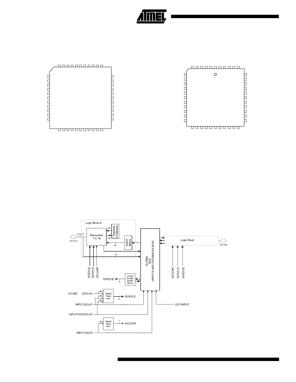
44-Lead TQFP/PQFP
Top View
I/O
I/O
I/O/PD1
VCC/PD2
I/OE2/GCK2
GCLR/I
I/OE1
GCK1/I
GND
GCK3
I/O
4443424140393837363534
33
I/O
I/O
32
I/O/TDO
31
I/O
30
I/O
29
VCC
28
I/O
27
I/O
26
I/O/TCK
25
I/O
24
GND
23
I/O
I/O/TDI
I/O
I/O
GND
PD1/I/O
I/O
TMS/I/O
I/O
VCC
I/O
I/O
1
2
3
4
5
6
7
8
9
10
11
1213141516171819202122
I/O
I/O
I/O
I/O
VCC
GND
I/O
I/O
I/O
I/O
Description
The ATF1502AS is a high pe rforman ce, hig h densi ty Complex Programmable Logic Device (CPLD) which utilizes
Atmel’s proven electric ally erasable techn ology. With 32
logic macrocell s and up to 36 inputs, it ea sily integra tes
logic from several TTL, SSI,MSI, LSI and classic PLDs.
The ATF1502AS’s enhanced routing switch matrices
increase usable gate count, and the odds of successful pinlocked design modifications.
44-Lead PLCC
Top View
I/O
I/O
I/O/PD1
VCC/PD2
GCK2/OE2/I
GCLR/I
OE1/I
GCK1/I
GND
I/O/GCLK3
I/O
TDI/I/O
I/O
I/O
GND
PD1/I/O
I/O
I/O/TMS
I/O
VCC
I/O
I/O
65432
7
8
9
10
11
12
13
14
15
16
17
1819202122232425262728
I/O
I/O
I/O
I/O
GND
1
VCC
4443424140
I/O
I/O
I/O
PD2/I/O
39
38
37
36
35
34
33
32
31
30
29
I/O
I/O
I/O/TDO
I/O
I/O
VCC
I/O
I/O
I/O/TCK
I/O
GND
I/O
The ATF1502AS has up to 32 bi-directional I/O pins and 4
dedicated input pins, depending on the type of device package selected. Each dedicated pin can also serve as a global control signal; reg ister clock, r egister reset or outp ut
enable. Each of these con trol sig nals can be select ed for
use individually within each macrocell.
Block Diagram
32
Each of the 32 macrocells generates a buried feedback,
which goes to the gl obal bus . Each in put and I/O pin also
B
feeds into the global bus. The switch matrix in each logic
block then selects 40 individual signals from the global bus.
2
ATF1502AS
ATF1502AS
Each macrocell also generates a foldback logic term, which
goes to a regional bus. Cas cade logi c betwe en macroc ells
in the ATF1502AS allows fast, effi cient ge nerati on of complex logic functions. The ATF1502AS contains four such
logic chains, each capable of creating sum term logic with a
fan in of up to 40 product terms.
The ATF1502AS macrocell shown in Figure 1, is flexible
enough to suppor t h igh ly co m ple x lo gi c func ti ons o per at ing
at high speed. The ma crocell consists of five sections :
product terms and product term select multiplexer;
OR/XOR/CASCADE logic; a flip-flop; output sel ect and
enable; and logic array inputs.
Unused product terms are automatic ally disabled by the
compiler to decrease power consumption. A Security Fuse,
Figure 1.
ATF1502AS Macrocell
when programmed, protects the contents of the
ATF1502AS. Two bytes (16-bits) of User Signature are
accessible to the user for purposes such as storing project
name, part number, revision or date . Th e Use r Sig natu re is
accessible regardless of the state of the Security Fuse.
The ATF1502AS device is an In-System Programmable
(ISP) device. It us es the industry stan dard 4-pin JTAG
interface (IEEE Std. 1149.1), and is fully compliant with
JTAG’s Boundary Scan Description Language (BSDL). ISP
allows the device to b e programmed with out removing it
from the printed circuit board. In addition to simplifying the
manufacturing flow, ISP also allows design modifications to
be made in the field via software.
Product Terms and Select MUX
Each ATF1502AS macrocell has five product terms. Each
product term recei v es as its i nputs all signals fr om both the
global bus and regional bus.
The product term selec t multi plex er (PTMU X) allo cates the
five product terms as needed to the macrocel l logic g ates
and control signals. The PTMUX programming is determined by the design compiler, wh ich sel ects the opti mum
macrocell configuration.
OR/XOR/CASCADE Logic
The ATF1502AS’s logic structure is designed to efficiently
support all types of logic. Within a single macrocell, all the
product terms can be routed to the OR gate, creating a 5input AND/OR sum term. With the addition of the CASIN
from neighboring macrocells, this can be expanded to as
many as 40 product terms with a very small additional
delay.
The macrocell’s XOR gate allows efficient implementation
of compare and arithmeti c function s. One inpu t to the XOR
comes from the OR sum term. The other XOR input can be
a product term or a fixed high or low level. For combinatorial outputs, the fixe d level in put allows pol arity sele ction.
For registered func tions, the fi xed levels al low DeMorgan
minimization of product terms. The XOR gate is also used
to emulate T- and JK-type flip-flops.
Flip Flop
The ATF1502AS’s flip flop has very flexible data and control functions. The data input can come from either the XOR
gate, from a separate product term or directly from the I/O
pin. Selectin g the se parat e produc t term allows c reatio n of
a buried registered feedback within a combinatorial output
3
macrocell. (This feature is automatically implemented by
the fitter softwa re). In add ition to D, T , JK and SR op eration, the flip flop can also be configured as a flow-through
latch. In this mode, data passes through when the clock is
high and is latched when the clock is low.
The clock itself c an eit her be on e o f the Glo bal CLK Sig nal
GCK[0 : 2] or an indi vidual product term . The flip flop
changes state on the clock’s rising edge. When the GCK
signal is used as the clock, one of the macrocell product
terms can be selecte d as a clock e nable . When t he cloc k
enable function is active and the enable signal (product
term) is low, all clock edges are ignored. The flip flop’s
asynchronous reset signal (AR) can be either the Global
Clear (GCLEAR), a product term, or always off. AR can
also be a logic OR of GCLEAR with a prod uct term. The
asynchronous pres et ( AP ) can be a pr odu ct te rm or al ways
off.
Output Select and Enable
The ATF1502AS ma crocel l outpu t can be s electe d as registered or combinatorial. The buried feedback signal can be
either combinatorial or registered signal regardless of
whether the output is combinatorial or registered.
The output enable multiplexer (MOE) controls the output
enable signals . Any buffer ca n be per manen tly en abled for
simple output operation. Buffers can also be permanently
disabled to allow use of the pin as an inp ut. In this config uration all the ma croce ll r eso urces ar e st ill avai labl e, i ncluding the buried feedback, exp ander and CASCADE log ic.
The output enabl e for each macroce ll can be se lected as
either of the two dedicated OE input pins as an I/O pin configured as an input, or as an individual product term.
Global Bus/Switch Matrix
The global bus contains all input and I/O pin signals as well
as the buried feedback si gnal from a ll 32 macroc ells. The
Switch Matrix in each Logic Block receives as its inputs all
signals from the global bus. Unde r software control, up to
40 of these signals can be selected as inputs to the Logic
Block.
Foldback Bus
Each macrocell a lso genera tes a foldback product term .
This signal goes to the regional bus and is available to 4
macrocells. The foldback is an inverse polarity of one of the
macrocell’s product terms. The 4 foldback terms in each
region allows generation of high fan-in sum terms (up to 9
product terms) with a small additional delay.
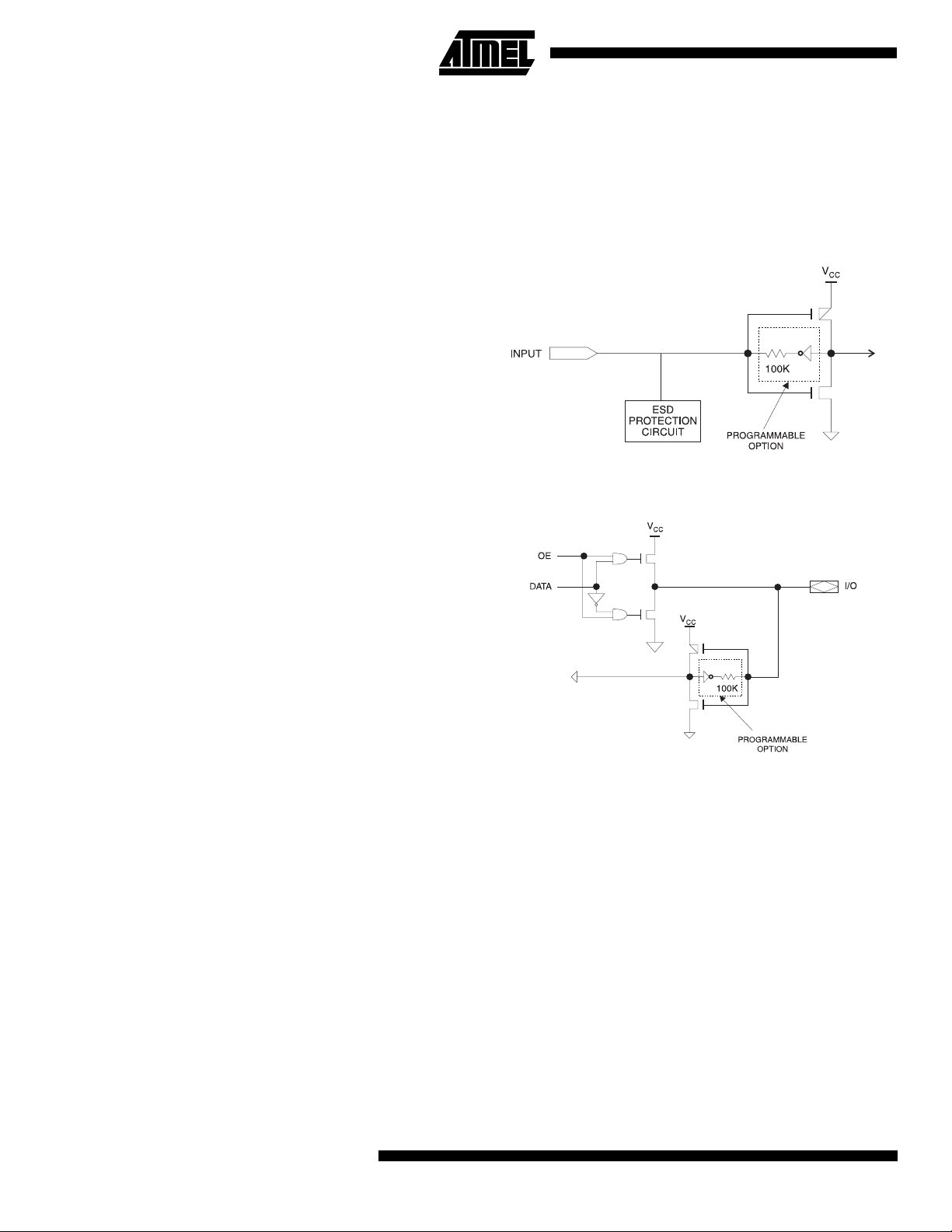
Programmable Pin-Keeper Option for
Inputs and I/Os
The ATF1502AS offers the op tion o f pro grammin g a ll inpu t
and I/O pins so that pin keep er circuits can be utilized .
When any pin is driven high or low and then subsequently
left floating, it will stay at that previous high or low level .
This circuitry prev ents unused input and I/O lines from
floating to i nterme diate v olt age l eve ls, which cau se u nnec essary power consumption and system noise. The keeper
circuits eliminate the need for external pull-up resistors and
eliminate their DC power consumption.
Input Diagram
I/O Diagram
Speed/Power Management
The ATF1502AS has several built-in speed and power
management features. The ATF1502AS contains circuitry
that automatically puts the device into a low power standby mode when no logic trans itions are oc curring. This not
only reduces power consumption during inactive periods,
but also prov ides a p roportion al power savings for most
applications runni ng at system sp eed s below 50 MHz. This
feature may be selected as a design option.
To further reduce power, each ATF1502AS macrocell has
a Reduced Power bit feat ur e. Th is fe atur e allows i ndiv idu al
macrocells to be c onfigur ed for maxi mum pow er sav ings.
This feature may be selected as a design option.
The ATF1502ASs also has an op tional po wer down mo de.
In this mode, current d rops to below 10 m A. When t he
power down option is selected, either PD1 or PD2 pins (or
both) can be used to power down the part. The power down
4
ATF1502AS

ATF1502AS
option is selecte d in the de sign sour ce file . When ena bled,
the device goes into power down when either PD1 or PD2
is high. In the power down mo de, all internal logic signa ls
are latched and held, as are any enabled outputs.
All pin transitions are ignored until the PD pin is brought
low. When the power down feature is enabled, the PD1 or
PD2 pin cannot be used as a logic input or output. However, the pin’s macr ocell m ay st ill be used to gen erate bur ied foldback and cascade logic signals.
All Power-Down AC Ch aracteristic parameters are computed from external input or I/O pins, with Reduced Power
Bit turned on. For mac rocells in reduced- power mode
(Reduced power bit turned on), the reduced power adder,
tRPA, must be added to the AC param eters, whic h include
the data paths t
LAD
LAC
, tIC, t
ACL
, t
ACH
and t
SEXP
.
, t
The ATF1502AS macrocell also has an option whereby the
power can be reduced on a per macrocell basis. By
enabling this power down option, macrocells that are not
used in an application can be turned down thereby reducing the overall power consumption of the device.
Each output also ha s i ndi vi dua l s lew r ate co n trol. This may
be used to reduce system noise by slowing down outputs
that do not need to operate at maximum speed. Outputs
default to slow switching , and may be speci fied as fast
switching in the design file.
Design Software Support
ATF1502AS des igns are su pported by s everal thi rd party
tools. Automated fitters allow logic synthesis using a variety
of high level description languages and formats.
Power Up Reset
The ATF1502AS has a power-up reset option at two different voltage trip levels when the device is being powered
down. Within the fitter, or during a conversion, if the
“power-reset” option is turned “on” (which is the default
option), the trip levels during power up or power down is at
2.8V. The user can change this default option from “on” to
“off” (within the fitter or specify it as a switch during conversion). When th is is done, the volt age trip level duri ng
power-down changes from 2.8V to 0.7V. This is to ensure a
robust operating environment.
The registers in the A TF1502AS are designed to r es et during power up. At a point delayed slightl y from V
Vrst, all registers will be reset to the low state. The output
state will depend on the polarity of the buffer.
This feature is critical for state machine initialization. However, due to the asynchronous nature of reset and the
uncertainty of how V
actually rises in the sy stem, the fol -
CC
lowing conditions are required:
crossing
CC
1. The V
rise must be monotonic,
CC
2. After reset occurs, all input and feedback setup
times must be met before driving the clock pinhigh, and,
3. The clock must remain stable during T
.
D
Security Fuse Usage
A single fuse is provided to preven t unauthorized copy ing
of the ATF1502AS fuse patterns. Once programmed, fuse
verify is inhibited. However, the 16-bit User Signature
remains accessible.
Programming
ATF1502AS devices are In-System Programmable (ISP)
devices utilizing the 4-pin JTAG protocol. This capability
eliminates package handling normally r equir ed fo r p ro gra m
and facilitates rapid design iterations and field changes.
Atmel provides ISP hardware and so ftware to allow programming of the ATF1502AS v ia the PC. ISP is perfo rmed
by using either a downlo ad cab le, or a compar able b oard
tester or a simple microprocessor interface.
When using the ISP hardware or S/W to program the
ATF1502AS devices, fo ur I/0 pi ns mus t b e res er ved for the
JTAG interface. However, the logic features the macrocells
associated with these I/0 pins are still available to the
design for burned logic functions.
To facilitate ISP program ming by the Automated Test
Equipment (ATE) vendors. Serial Vector Format (SV F) file s
can be created by Atmel provided Software utilities.
ATF1502AS devices can also be programmed using standard 3rd party programmers. With 3rd party programmer
the JTAG ISP port can be disabled thereby allowing 4 additional I/O pins to be used for logic.
Contact your local Atmel representatives or Atmel PLD
applications for details.
ISP Programming Protection
The ATF1502AS has a special feature which locks the
device and pr events the in puts a nd I/O from drivin g if t he
programming process is interrupted due to any reason. The
inputs and I/O default to high-Z state during such a c ondition. In addition, th e pin keeper option pr eserve s the previous state of the input and I/0 PMS during programming.
All ATF1502AS devices are initially shipped in the erased
state thereby making them ready to use for ISP.
Note: For more information refer to the “Designing for In-Sys-
tem Programmability with Atmel CPLDs” application
note.
5
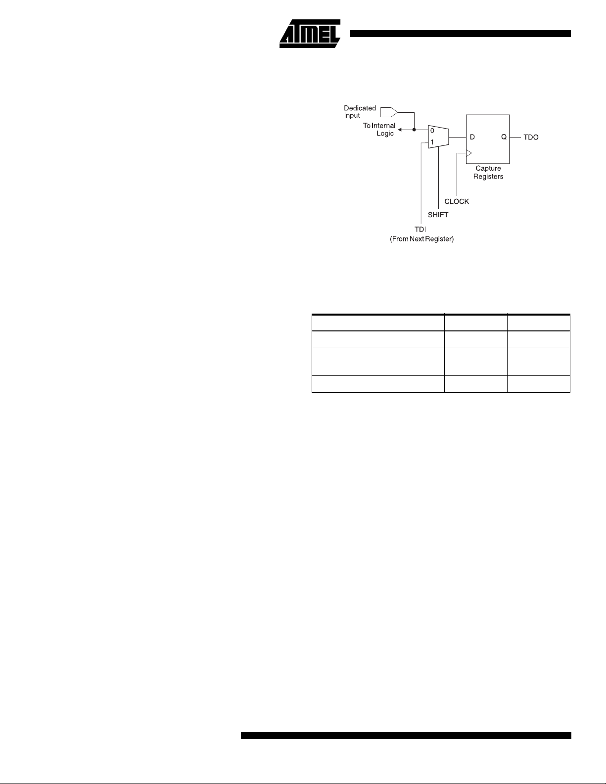
JTAG-BST/ISP Overview
The JTAG boundary-scan testing is controlled by the Test
Access Port (TAP) controller in the ATF1502AS. The
boundary-scan technique invol ves the inc lusion of a sh iftregister stage (con tained in a bound ary-s can c ell) adj acen t
to each component so that signals at component boundaries can be controlled a nd observed u sing scan test ing
methods. Each input pin and I/O pin has its own boundary
scan cell (BSC) to s upport boundar y scan testing. Th e
ATF1502AS does not include a Test Reset (TRST) input
pin because the TAP controller is automatically reset at
power up. The five JTAG modes supported include: SAMPLE/PRELOAD, EXTEST, BYPASS, IDCODE and HIGHZ.
The ATF1502AS’s ISP can be fully described using JTAG’s
BSDL as described in IE EE S tandar d 114 9.1b. Th is a llows
ATF1502AS progr amming to be descri bed and implemented using any on e of the 3 rd par ty developm ent tools
supporting this standard.
The ATF1502AS has the opti on of using fou r JTAG-s tandard I/O pins for boundary s can testing (BST) and in -system programming (ISP) purposes. The ATF1502AS is
programmable through the four JTAG pins using the IEEE
standard JTAG programmi ng protocol establ ished by IEEE
Standard 1149.1 using 5V TTL-level programming signals
from the ISP interface fo r in-system programming. T he
JTAG feature is a progr ammable opt ion. If JTAG (BS T or
ISP) is not needed, then the four JTAG control pins are
available as I/O pins.
BSC Configuration for Input and I/O
Pins (except JTAG TAP Pins)
Note: The ATF1502AS has pull-up option on TMS and TDI
pins. This feature is selected as a design option.
DC and AC Operating Conditions
Commercial Industrial
Operating Temperature (Case) 0°C - 70°C-40°C - 85°C
V
or V
CCINT
Supply
(3.3V) Power Supply 3.0V - 3.6V 3.0V - 3.6V
V
CCIO
(5V) Power
CCIO
5V ± 5% 5V ± 10%
JTAG Boundary Scan Cell (BSC)
Testing
The ATF1502AS contains up to 32 I/O pins and 4 input
pins, depe nding on th e an d pac kage type sele cted. Each
input pin and I/O pin has its ow n bound ary scan cell (BSC)
in order to sup port bou ndary scan t esting a s desc ribed in
detail by IEEE Standard 1149.1. Typical BSC consists of
three capture register s or scan regis ters and up to two
update registers. There are two types of BSCs, one for
input or I/O pin, and on e for the macroce lls. The BSCs in
the device are chaine d togeth er thro ugh the captur e regis ters. Input to the capture register chain is fed in from the
TDI pin while the output is directed to the TDO pin. Capture
registers are used to capture active device data signals, to
shift data in and out of the de vice an d to load data into the
update regist ers. Contr ol signals are gener ated inte rnally
by the JTAG TAP con troller . The B SC config urati on for the
input and I/O pins and macrocells are shown below.
6
ATF1502AS

ATF1502AS
DC Characteristics
Symbol Parameter Condition Min Typ Max Units
I
IL
I
IH
I
OZ
I
CC1
I
CC2
I
CC3
I
OS
V
CCIO
V
CCIO
V
IL
V
IH
Input or I/O Low
Leakage Cu rrent
Input or I/O High
Leakage Cu rrent
Tri-State Output
Off-State Current
V
IN
= V
CC
-2 -10 µA
210
= VCC or GND -40 40 µA
V
O
Com. 60 mA
Std Mode
Po wer Supply Current ,
Stand-by
VCC = Max
= 0, V
V
IN
CC
Ind. 75 mA
Com. 40 µA
“Z” Mode
Ind. 40 µA
Po wer Supply Current ,
Power Down Mode
Clocked Power Supply
Current
Output Short Circuit
Current
VCC = Max
= 0, V
V
IN
CC
VCC = Max
= 0, V
V
IN
V
OUT
CC
= 0.5V -150 mA
“PD” Mode 1 mA
“Z” Mode 2
mA/
MHz
Com. 4.75 5.25 V
Supply Voltage 5.0V Device Output
Ind. 4.5 5.5 V
Supply Voltage 3.3V Device Output 3.0 3.6 V
Input Low Voltage -0.3 0.8 V
+
V
Input High Voltage 2.0
CCINT
0.3
V
V
OL
V
OH
Output Low Voltage
Output High Voltage
VIN = VIH or V
V
= MIN, IOL = 12 mA
CCIO
= VIH or V
V
IN
V
= MIN, IOH = -4.0 mA
CCIO
IL
IL
Com. 0.45 V
Ind.
2.4 V
Note: Not more than one output at a time should be shorted. Duration of short circuit test should not exceed 30 sec.
Pin Capacitance
Typ Max Units Conditions
C
IN
C
I/O
Note: Typical values for nominal supply voltage. This parameter is only sampled and is not 100% tested.
The OGI pin (high-voltage pin during programming) has a maximum capacitance of 12 pf.
810pF V
810pF V
= 0V; f = 1.0 MHz
IN
= 0V; f = 1.0 MHz
OUT
7
Absolute Maximum Ratings*
Temperature Under Bias.................................. -40°C to +85°C
Storage Temperature..................................... -65°C to +150°C
Voltage on Any Pin with
Respect to Ground .........................................-2.0V to +7.0V
Voltage on Input Pins
with Respect to Ground
During Programming.....................................-2.0V to +14.0V
Programming Voltage with
Respect to Ground .......................................-2.0V to +14.0V
AC Characteristics
-7 -10 -15 -20 -25
*NOTICE: Stresses beyond those listed under “Absolute
Maximum Ratings” may cause permanent damage to the dev ice . This is a s tress rating only an d
functional oper ation of the device at these or any
(1)
other conditions beyond those indicated in the
operational sections of this specification is not
implied. Exposure to absolute maximum rating
conditions f or e xtended periods ma y af fect de vice
(1)
reliability .
Note: 1. Minimum voltage is -0.6V DC, which may under-
shoot to -2.0V for pulses of less than 20 ns. Max-
(1)
imum output pin voltage is V
which may overshoot to 7.0V for pulses of less
+ 0.75V DC,
CC
than 20 ns.
Symbol Parameter
t
PD1
t
PD2
t
SU
t
H
t
FSU
t
FH
t
COP
t
CH
t
CL
t
ASU
t
AH
t
ACOP
t
ACH
t
ACL
t
CNT
f
CNT
Input or Feedback to
Non-Registered Output
I/O Input or Feedback to
Non-Registered Feedback
Global Clock Setup Time 6 7 11 16 20 ns
Global Clock Hold Time 0 0 0 0 0 ns
Global Clock Setup Time of
Fast Input
Global Clock Hold Time of
Fast Input
Global Clock to Output Delay 4.5 5 8 10 13 ns
Global Clock High Time 3 4 5 6 7 ns
Global Clock Low Time 3 4 5 6 7 ns
Array Clock Setup Time 3 3 4 4 5 ns
Array Clock Hold Time 2 3 4 5 6 ns
Array Clock Output Delay 7.5 10 15 20 25 ns
Array Clock High Time 3 4 6 8 10 ns
Array Clock Low Time 3 4 6 8 10 ns
Minimum Clock Global Period 8 10 13 17 22 ns
Maximum Internal Global
Clock Frequency
UnitsMin Max Min Max Min Max Min Max Min Max
7.5 10 3 15 20 25 ns
793121625ns
33335ns
0.5 0.5 1 1.5 2 MHz
125 100 76.9 66 50 MHz
t
ACNT
f
ACNT
8
Minimum Array Clock Period 8 10 13 17 22 ns
Maximum Internal Array
Clock Frequency
125 100 76.9 66 50 MHz
ATF1502AS

AC Characteristics (Continued)
Symbol Parameter
ATF1502AS
-7 -10 -15 -20 -25
UnitsMin Max Min Max Min Max Min Max Min Max
F
t
IN
t
IO
t
FIN
t
SEXP
t
PEXP
t
LAD
t
LAC
t
IOE
MAX
Maximum Clock Frequency 166.7 125 100 83.3 60 MHz
Input Pad and Buffer Delay 0.5 0.5 2 2 2 ns
I/O Input Pad and Buffer Delay 0.5 0.5 2 2 2 ns
Fast Input Delay 1 1 2 2 2 ns
Foldback Term Delay 4 5 8 10 12 ns
Cascade Logic Delay 0.8 0.8 1 1 1.2 ns
Logic Array Delay 3 5 6 7 8 ns
Logic Control Delay 3 5 6 7 8 ns
Internal Output Enable Delay 2 2 3 3 4 ns
Output Buffer and Pad Delay
t
OD1
(Slow slew rate = OFF;
= 5V; CL = 35 pF)
V
CCIO
Output Buffer and Pad Delay
t
OD2
(Slow slew rate = OFF;
= 3.3V; CL = 35 pF)
V
CCIO
Note: See ordering information for valid par t numbers.
Timing Model
21.5 4 5 6ns
2.5 2.0 5 6 7 ns
(continued)
9

AC Characteristics (Continued)
-7 -10 -15 -20 -25
Symbol Parameter
Output Buffer Enable Delay
t
ZX1
(Slow slew rate = OFF;
= 5.0V; CL = 35 pF)
V
CCIO
Output Buffer Enable Delay
t
ZX2
(Slow slew rate = OFF;
= 3.3V; CL = 35 pF)
V
CCIO
Output Buffer Enable Delay
t
ZX3
t
XZ
t
SU
t
H
t
FSU
t
FH
t
RD
t
COMB
t
IC
t
EN
t
GLOB
t
PRE
t
CLR
t
UIM
t
RPA
(Slow slew rate = ON;
= 5.0V/3.3V; CL = 35 pF)
V
CCIO
Output Bu ffer Disable Delay
= 5 pF)
(C
L
Register Setup Time 3 3 4 5 6 ns
Register H old Time 2 3 4 5 6 ns
Register Setup Time of Fast Input 3 3 2 2 3 ns
Register Hold Time of Fast Input 0.5 0.5 2 2 2.5 ns
Register D elay 1 2 1 2 2 ns
Combinatorial Delay 1 2 1 2 2 ns
Array Clock Delay 35678ns
Register Enable Time 3 5 6 7 8 ns
Global Control Delay 1 1 1 1 1 ns
Register Preset Time 23456ns
Register C lear Time 2 3 4 5 6 ns
Switch Matrix Delay 11222ns
Reduced-Power Adder
(2)
Notes: 1. See ordering information for valid part numbers.
2. The t
parameter must be added to the t
RPA
LAD
, t
power mode.
UnitsMinMaxMinMaxMinMaxMinMaxMinMax
4.0 5.0 7 9 10 ns
4.5 5.5 7 9 10 ns
9 9 10 11 12 ns
45678ns
10 11 13 14 15 ns
, t
LAC,tTIC
ACL
, and t
parameters for macrocells running in the reduced-
SEXP
Input Test Waveforms and
Measurement Levels
tR, tF = 1.5 ns typical
10
ATF1502AS
Output AC Test Loads
(3.0V)*
(703 )*
(8060 )*
Note: *Numbers in parenthesis refer to 3.0V operating condi-
tions (preliminary)

Power Down Mode
The ATF1502AS i nclud es an opti onal pi n contro lled powe r
down feature.When this mode is enabled, the PD pin acts
as the power down pin. When the PD pin is high, the device
supply curre nt is red uced t o less th an 3 mA. During po wer
down, all output data and internal log ic states ar e latched
and held. Therefore, all registered and combinatorial output
data remain va lid. Any out puts which were in a Hi-Z stat e at
the onset will remain at Hi-Z. During power down, all input
ATF1502AS
signals except the power down pin are blocked. Input and
I/O hold latche s remain activ e to insure th at pins do not
float to indeterminate levels, further reducing system
power. The power down pin feature is enabled in the logic
design file. Designs us in g the power down pin may not u se
the PD pin logic array input. However, all other PD pin macrocell resources may s till be used, includin g the buried
feedback and foldback product term array inputs.
P ower Down AC Characteristics
Symbol Parameter
t
IVDH
t
GVDH
t
CVDH
t
DHIX
t
DHGX
t
DHCX
t
DLIV
t
DLGV
t
DLCV
t
DLOV
Notes: 1. For slow slew ou tputs, add t
Valid I, I/O Before PD High 7 10 15 20 25 ns
Valid OE
Valid Clock
(2)
Before PD High 7 10 15 20 25 ns
(2)
Before PD High 7 10 15 20 25 ns
I, I/O Don’t Care After PD High 12 15 25 30 35 ns
(2)
OE
Don’t Care After PD High 12 15 25 30 35 ns
(2)
Clock
Don’t Care After PD High 12 15 25 30 35 ns
PD Low to Valid I, I/O 1 1 1 1 1
PD Low to Valid OE (Pin or Term) 1 1 1 1 1
PD Low to Valid Clock (Pin or Term) 1 1 1 1 1
PD Low to Valid Output 1 1 1 1 1
.
SSO
2. Pin or Product Term.
(1)(2)
-7 -10 -15 -20 -25
UnitsMinMaxMinMaxMinMaxMinMaxMinMax
s
µ
s
µ
s
µ
s
µ
11

BSC Configuration for Mac
BSC for Dedicated Input
TDO
TDO
Q
OEJ
D
CLOCK
0
1
0
Pin
0
1
TDI
TDO
DQ
1
TDI
Shift
DQ
DQ
Capture
DR
Clock
0
1
12
OUTJ
0
1
TDI
Shift
ATF1502AS
DQ
Capture
DR
BSC for I/O Pins and Macrocells
DQ
Update
DR
Clock
0
1
Pin
Mode

ATF1502AS
PCI Compliance
The ATF1502AS also supports the growing need in the
industry to support the new Peripheral Component Interconnect (PCI) interface standard in PCI-based designs and
specifications . The PCI interfa ce calls fo r high curren t drivers which are much larger than the traditional TTL drivers.
high current load required by th e PCI interface. The
ATF1502AS allows this without contributing to system
noise while delivering low output to output skew. Having a
programmable h igh drive option is also pos sible with out
increasing output delay or pin capacitance. The PCI electrical characteristics appear on the next page.
In general, PLDs and FPGAs parallel outputs to support the
PCI Voltage-to-Current Curves for +5V Signaling in Pull-Up Mode
point
Pull Up
-44
Current (mA)
Test Point
-178
VCC
2.4
1.4
Voltage
DC
drive point
AC drive
-2
PCI Voltage-to-Current Curves for +5V Signaling in Pull-Down Mode
VCC
Voltage
2.2
DC
drive point
0.55
3.6
AC drive
point
Pull Down
95
Test Point
Current (mA)
380
13

PCI DC Characteristics (Preliminary)
Symbol Parameter Conditions Min Max U nits
V
V
V
I
IH
I
IL
V
V
C
C
C
L
CC
IH
IL
OH
OL
IN
CLK
IDSEL
PIN
Supply Voltage 4.75 5.25 V
Input High Voltage 2.0 VCC + 0.5 V
Input Low Voltage -0.5 0 .8 V
Input High Leakage Current VIN = 2.7V 70 µA
Input Low Leakage Current VIN = 0.5V -70 µA
Output High Voltage I
Output Low Voltage I
= -2 mA 2.4 V
OUT
= 3 mA, 6 mA 0.55 V
OUT
Input Pin Capacitance 10 pF
CLK Pin Capacitance 12 pF
IDSEL Pin Capacitance 8 pF
Pin Inductance 20 nH
Note: Leakage Current is with Pin-Keeper off.
PCI AC Characteristics (Preliminary)
Symbol Parameter Conditions Min Max Units
I
OH(AC)
I
OL(AC)
I
CL
Switching 0 < V
Current High 1.4 < V
3.1 < V
(Test High) V
Switching V
Current Low 2.2 > V
0.1 > V
(Test Point) V
≤ 1.4 -44 mA
OUT
OUT
OUT
= 3.1V -142 µA
OUT
> 2.2V 95 mA
OUT
OUT
OUT
= 0.71 206 mA
OUT
Low Clamp Current -5 < VIN ≤ -1
< 2.4
< V
CC
-44+(V
> 0 V
- 1.4)
OUT
/0.024
Equation A mA
/0.023 mA
OUT
> 0 Equation B mA
IN
+ 1)
-25+(V
/0.015
mA
mA
SLEW
SLEW
Output Rise Slew Rate 0.4V to 2.4V load 1 5 V/ns
R
Output Fall Slew Rate 2.4V to 0.4V load 1 5 V/ns
F
Notes: 1. Equation A: I
2. Equation B: IOL = 78.5 * V
14
= 11.9 (V
OH
- 5.25) * (V
OUT
* (4.4 - V
OUT
ATF1502AS
+ 2.45) for VCC > V
OUT
) for 0V < V
OUT
< 0.71V.
OUT
OUT
> 3.1V.

ATF1502AS Dedicated Pinouts
ATF1502AS
44-Pin
Dedicated Pin
INPUT/OE2/GCLK2 40 2 40
INPUT/GCLR 39 1 39
INPUT/OE1 38 44 38
INPUT/GCLK1 37 43 37
I/O /GCLK3 35 41 35
I/O / PD (1,2) 5, 19 11, 25 5, 19
I/O / TDI (JTAG) 1 7 1
I/O / TMS (JTAG) 7 13 7
I/O / TCK (JTAG) 26 32 26
I/O / TDO (JTAG) 32 38 32
GND 4, 16, 24, 36 10, 22, 30, 42 4, 16, 24, 36
V
CCINT
V
CCIO
N/C --# of Signal Pins 36 36 36
# User I/O Pins 32 32 32
TQFP
9, 17, 29, 41 3, 15, 23, 35 9, 17, 29, 41
---
44-Pin
J-Lead
44-Pin
PQFP
OE (1, 2) Global OE Pins
GCLR Global Clear Pin
GCLK (1, 2, 3) Global Clock Pins
PD (1, 2) Power down pins
TDI, TMS, TCK, TDO JTAG pins used for Boundary Scan Testing or In-System Programming
GND Ground Pins
V
V
CCINT
CCIO
VCC pins for the device (+5V - Internal)
VCC pins for output drivers (for I/O pins) (+5V or 3.3V - I/Os)
15

ATF1502AS I/O Pinouts
MC PLC 44-Pin PLCC 44-Pin TQFP 44-Pin PQFP
1A4 4242
2A5 4343
3A/PD1 64141
4A7 1 1
5A8 2 2
6A9 3 3
7A11 5 5
8/TDI A12 6 6
9A13 7 7
10 A 14 8 8
11A161010
12A171111
13A181212
14A191313
15A201414
16A211515
17B413535
18B403434
19B393333
20B383232
21B373131
22B363030
23B342828
24B332727
25B322626
26B312525
27B292323
28B282222
29B272121
30B262020
31B251919
32/TMS B241818
16
ATF1502AS

Ordering Information
t
PD
(ns)
7.5 4.5 166.7 ATF1502AS-7 AC44
10 5 125 ATF1502AS-10 AC44
10 5 125 ATF1502AS-10 AI44
15 8 100 ATF1502AS-15 AC44
15 8 100 ATF1502AS-15 AI44
20 12 83.3 ATF1502ASL-20 AC44
20 12 83.3 ATF1502ASL-20 AI44
25 15 70 ATF1502ASL-25 AC44
25 15 70 ATF1502ASL-25 AI44
t
CO1
(ns)
f
MAX
(MHz) Ordering Code Packa ge Operation Range
ATF1502AS-7 JC44
ATF1502AS-7 QC44
ATF1502AS-10 JC44
ATF1502AS-10 QC44
ATF1502AS-10 JI44
ATF1502AS-10 QI44
ATF1502AS-15 JC44
ATF1502AS-15 QC44
ATF1502AS-15 JI44
ATF1502AS-15 QI44
ATF1502ASL-20 JC44
ATF1502ASL-20 QC44
ATF1502ASL-20 JI44
ATF1502ASL-20 QI44
ATF1502ASL-25 JC84
ATF1502ASL-25 QC44
ATF1502ASL-25 JI84
ATF1502ASL-25 QI44
44A
44J
44Q
44A
44J
44Q
44A
44J
44Q
44A
44J
44Q
44A
44J
44Q
44A
44J
44Q
44A
44J
44Q
44A
44J
44Q
44A
44J
44Q
ATF1502AS
Commercial
(0°C to 70°C)
Commercial
(0°C to 70°C)
Industrial
(-40°C to +85°C)
Commercial
(0°C to 70°C)
Industrial
(-40°C to +85°C)
Commercial
(0°C to 70°C)
Industrial
(-40°C to +85°C)
Commercial
(0°C to 70°C)
Industrial
(-40°C to +85°C)
Package Type
44A 44-Lead, Thin Plastic Gull Wing Quad Flatpack (TQFP)
44J 44-Lead, Plastic J-Leaded Chip Carrier OTP (PLCC)
44Q 44-Lead, Plastic Gull Wing Quad Flatpack (PQFP)
17

Packaging Information
.045(1.14) X 45°
PIN NO.1
IDENTIFY
.045(1.14) X 30° - 45°
.012(.305)
.008(.203)
.021(.533)
.013(.330)
.630(16.0)
.590(15.0)
.043(1.09)
.020(.508)
.120(3.05)
.090(2.29)
.180(4.57)
.165(4.19)
.500(12.7) REF SQ
.032(.813)
.026(.660)
.050(1.27) TYP
.022(.559) X 45° MAX (3X)
.656(16.7)
.650(16.5)
.695(17.7)
.685(17.4)
SQ
SQ
44A, 44-Lead, Thin (1.0 mm) Plastic Gull Wing
Quad Flat Package (TQFP)
Dimensions in Millimeters and (Inches)*
* Controlling dimension: millimeters
44J, 44-Lead, Plastic J-Leaded Chip Carrier (PLCC)
Dimensions in Inches and (Millimeters)
JEDEC STANDARD MS-018 AC
44Q, 44 Lead, Plastic Gull Wing Quad Flat
Package (PQFP)
Dimensions in Inches and (Millimeters)
* Controlling dimension: millimeters
18
ATF1502AS
 Loading...