

Page 1

ATEVK525 Mass Storage Board for AVR
..............................................................................................
Hardware User Guide
Page 2

Section 1
Introduction ........................................................................................... 1-3
1.1 Overview ...................................................................................................1-3
1.2 ATEVK525 AVR Mass Storage Board Features .......................................1-4
Section 2
Using the ATEVK525............................................................................ 2-5
2.1 Getting started ..........................................................................................2-5
2.2 NAND Flash ..............................................................................................2-7
2.3 SD/MMC Card.........................................................................................2-11
2.4 LEDs .......................................................................................................2-12
2.5 Test Points ..............................................................................................2-12
2.6 Configuration Pads .................................................................................2-13
2.7 Solder Pads ............................................................................................2-14
Section 3
Software Implementation .................................................................... 3-15
3.1 Software packages .................................................................................3-15
3.2 Performances..........................................................................................3-17
3.3 Driver limitations......................................................................................3-18
3.4 Usage Notes ...........................................................................................3-19
3.5 Handling another NAND Flash device ....................................................3-19
Section 4
Troubleshooting Guide ....................................................................... 4-21
Section 5
Technical Specifications ..................................................................... 5-23
Section 6
Technical Support............................................................................... 6-24
Section 7
Complete Schematics......................................................................... 7-25
ATEVK525 Mass Storage Board for AVR User Guide 1
7740B–AVR–03/08
Page 3

1.1 Overview
Section 1
Introduction
Congratulations on acquiring the AVR® ATEVK525. This kit is an extension board
designed to enhance and demonstrate Mass Storage features in addition to the existing
development boards supporting the AT90USBxxx family.
This document describes the ATEVK525 dedicated to the AT90USBxxx <Generic
Product Name> microcontroller. This board is designed to allow an easy evaluation of
USB Mass Storage using demonstration software.
The ATEVK525 board has been designed to be plugged into the Atmel STK525 Starter
Kit Board in order to add Mass Storage capability to an existing development board, and
to combine them with other features (USB, RS232, Microphone..., but also all AVR
development tools), reducing the extension board complexity and cost.
This user guide acts as a general getting started guide as well as a complete technical
reference for advanced users.
ATEVK525 Mass Storage Board for AVR 1-3
7740B–AVR–03/08
Page 4

Introduction
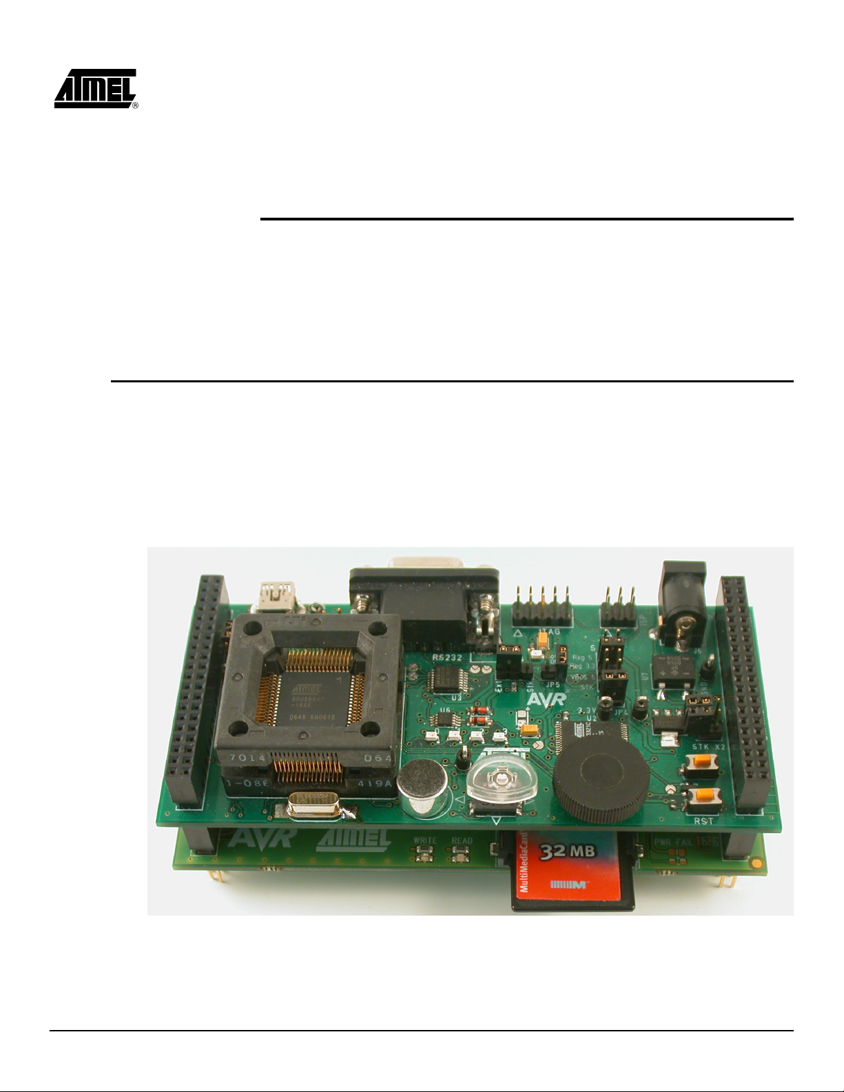
Figure 1-1 . ATEVK525
1.2 ATEVK525 AVR Mass Storage Board Features
The ATEVK525 provides the following features:
NAND Flash chip soldered (Micron MT29F2G08AACWP, 256 MBytes)
Reserved location additional NAND Flash chips module plug-in
Receptacle for SD and MMC memory cards
LED signalling for Read/Write operations
Power supply :
– 3.3V regulated from motherboard
– Additional overvoltage protection circuitry (optional) with failure indicator
Numerous access points for debug
1-4 ATEVK525 Mass Storage Board for AVR
7740B–AVR–03/08
Page 5
2.1 Getting started
2.1.1 Plugging the board
Section 2
Using the ATEVK525
This chapter describes the board and all its features.
The ATEVK525 is an extension board that must be plugged on another microcontroller
hosting board, like STK525 (AT90USBxxx support), that provides supply voltage.
Figure 2-1 . Connecting the ATEVK525 under the STK525
Note: The
ATEVK525 Mass Storage Board for AVR 2-5
ATEVK525 can also be plugged onto the STK525, but in this configuration,
the user must take care to avoid contact between the board and either the
JTAG plug or the microcontroller ZIF socket.
7740B–AVR–03/08
Page 6
Using the ATEVK525
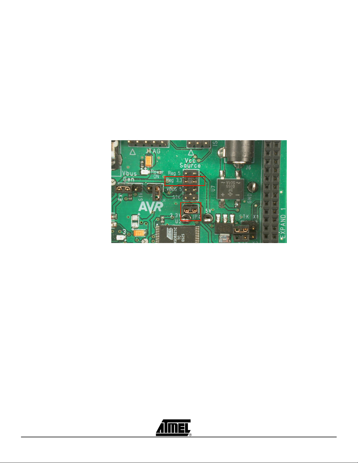
2.1.2 Power supply
The ATEVK525 must be powered with a voltage between 2.8 and 3.5V.
Before connecting or powering the boards, you must ensure the power supply
configuration on the motherboard.
The voltage must be set to 3.3V (microcontroller I/O levels), and this voltage must be
present on the VTG pins of the EXPAND connectors.
On the STK525, the configuration must be:
– JP4 closed (ties 3.3V to VTG pins)
– VCC SOURCE set to REG 3.3 mode (powers microcontroller I/O at 3.3V)
Figure 2-2 . Configuration to set on STK525
NAND Flash (MT29F2G08AACWP) current consumption is 1mA maximum in idle state,
and can reach 30mA (15mA typ.) during access operations (read/write/erase). For the
SD/MMC card consumption, please refer to your SD/MMC card datasheet.
2-6 ATEVK525 Mass Storage Board for AVR
7740B–AVR–03/08
Page 7
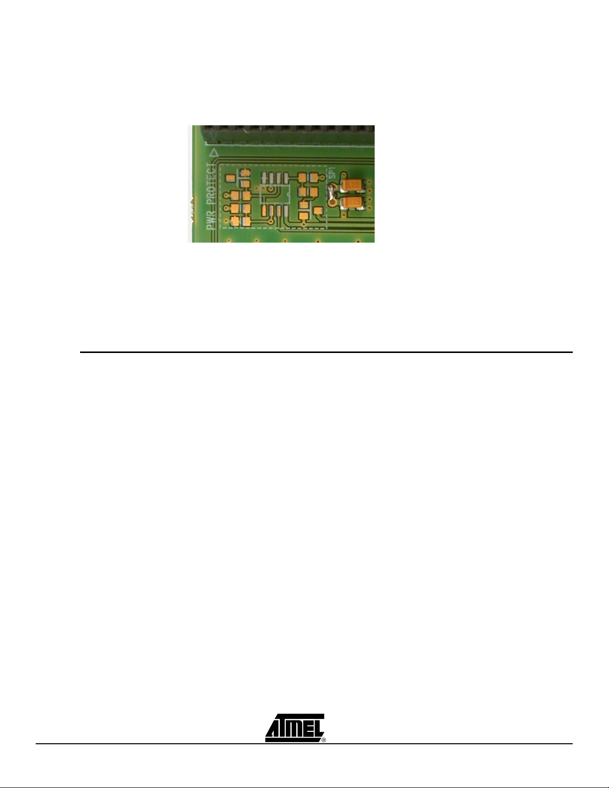
2.1.3 Protection circuitry
Using the ATEVK525
The ATEVK525 includes an optional power supply protection circuit that prevents onboard resources from being damaged.
Figure 2-3 . Power protection circuit location
This supplement, if mounted, protects the storage devices from voltage above 3.5V. In
case of overvoltage detection, the power positive line of the extension board is not
connected to devices, and the LED “PWR_FAIL” is lit.
If the supplement is not mounted or needs to be disabled, the solder pad SP1 must be
soldered to connect power supply of the on-board resources (see photo above).
2.2 NAND Flash
2.2.1 Default device
The ATEVK525 comes with one NAND Flash chip soldered. At the time of writing, this
chip is the Micron MT29F2G08AACWP that features:
2 GBits (256 MBytes) organized as:
– 2048 blocks
– block size : 64 pages
– page size : 2112 bytes (2048 + 64 in spare zone)
Page program time of 300µs, Block erase time of 2ms
Copy-Back feature (enable cache transfers between blocks to speed up write
operation; no memory zone / address limitation)
The memory access is managed by the External Memory Interface hardware peripheral
of the AT90USBxxx microcontroller. Data and Address information share the same 8-bit
wide bus connected to the lowest bits of Memory Interface (A7-A0), while the Control
signals are connected to upper bits:
ATEVK525 Mass Storage Board for AVR 2-7
7740B–AVR–03/08
Page 8
Using the ATEVK525
1
1
13
13
NFCON1
NFCON2
Table 2-1 . NAND Flash pin assignment
NAND Flash Microcontroller Function
I/O[7:0] PORTA[7:0] (A7-A0) Data and Address bus
CLE PORTC0 (A8) Command Latch Enable
ALE PORTC1 (A9) Data Latch Enable
RE# PORTE1 (RD#) Read enable
WE# PORTE0 (WR#) Write enable
CE# PORTC2 (A10) Chip select (active low) (with on-board pull-up)
R/B# PORTC6 Ready / Busy# (pull-up must be enabled in micro)
Note: The ‘#’ character indicates that the corresponding signal is active low.
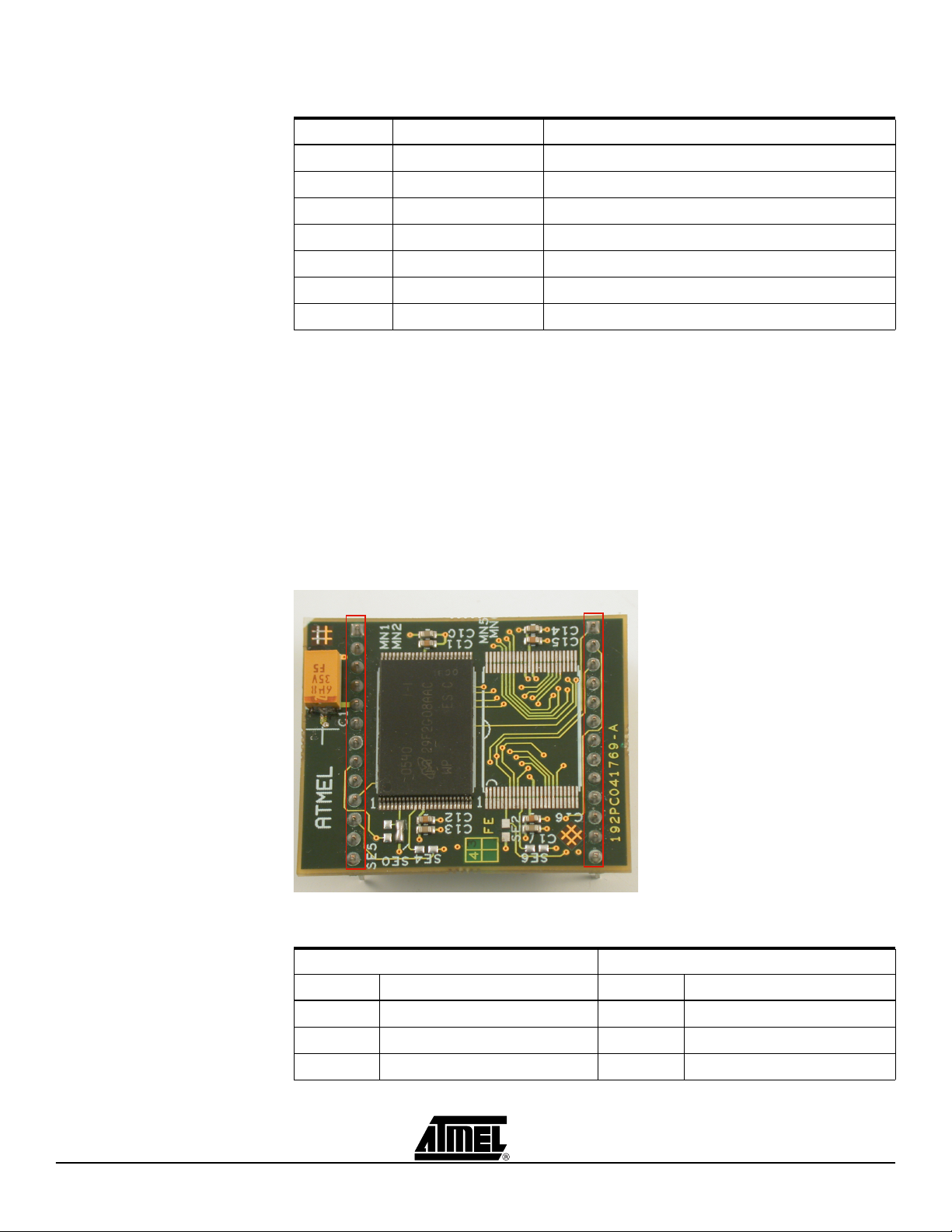
2.2.2 Additional devices
NAND Flash Module Description If another memory device is required for development or evaluation purpose, it is still
possible to install it on the ATEVK525 through an additional module as described below.
The board provides two SIP-13 receptacle footprints (2.54mm pitch). Users can solder a
receptacle on the board and then insert a NAND Flash module described below, or
directly solder the module.
Figure 2-4 . NAND Flash module example
Table 2-2 . NAND Flash module pin-out description
Pin # Function Pin # Function
1 WP2# 1 WP3#
NFCON1 NFCON2
2 CE3# 2 R/B3#
3 CE2# 3 R/B2#
2-8 ATEVK525 Mass Storage Board for AVR
7740B–AVR–03/08
Page 9

Using the ATEVK525
NFCON1 NFCON2
Pin # Function Pin # Function
4 WP0# 4 WP1#
5 VCC 5 D7
6 CLE 6 D6
7 ALE 7 D5
8 R/B1# 8 D4
9 CE0# 9 D3
10 R/B0# 10 D2
11 CE1# 11 D1
12 RE# 12 D0
13 WE# 13 GND
Refer to the CD-ROM documentation if you wish to create your own PCB board and
mount devices on this board (BOM and components placement).
Each module can receive up to four different devices, according to the following
placement :
Table 2-3 . NAND Flash devices placement
ATEVK525 Mass Storage Board for AVR 2-9
7740B–AVR–03/08
Page 10

Using the ATEVK525
See Note 1
NF Module Installation Figure 2-5 . NAND Flash module on the ATEVK525, plus MMC card
When using the NAND Flash module, the following pin assignments do not change :
Data/Address bus, CLE, ALE, RE#, WE#, WP# (Write Protect feature drives all the
chips at the same time). Other signal assignments are grouped in the following table.
Table 2-4 . NAND Flash module pin assignment
NAND Flash Microcontroller Function
CE0# PORTC2 (A10) Chip select for chip 0 (active low, on-board pull-up)
CE1# PORTC3 (A11) Chip select for chip 1 (active low, on-board pull-up)
CE2# PORTC4 (A12) Chip select for chip 2 (active low, on-board pull-up)
CE3# PORTC5 (A13) Chip select for chip 3 (active low, on-board pull-up)
R/B0# PORTC6 Ready / Busy# for chip 0 (pull-up to enable in micro)
R/B1# PORTC7 Ready / Busy# for chip 1 (pull-up to enable in micro)
R/B2# PORTD0 Ready / Busy# for chip 2 (pull-up to enable in micro)
R/B3# PORTD1 Ready / Busy# for chip 3 (pull-up to enable in micro)
Note: 1. When using the additional module, the resistor R10 must be unsoldered, else
the CE# lines of the NAND Flash soldered and the NAND Flash #0 of the module will be connected together (not applicable if NF #0 is not mounted on the
module)
2. When using the additional module, check that the configuration pads that enable
CTS/RTS lines on STK525 are not soldered, because these signals are also connected to the R/B#2 & 3. But if CTS/RTS lines are required, you cannot use the
R/B#2 & 3 signals, so disable the configuration pads CP1 & CP2 of the ATEVK525.
2-10 ATEVK525 Mass Storage Board for AVR
7740B–AVR–03/08
Page 11

2.3 SD/MMC Card
Using the ATEVK525
The ATEVK525 includes a receptacle compatible with SD and MMC memory cards.
Figure 2-6 . SD card pinout (contact view)
Note: 1. The MMC card defined by specification v3.31 and earlier have only the pins #1 to #7
2. The MMC card defined by specification v4.0 and later (MMC Plus, Extra..) has 13
pins (increasing parallel data bus width)
Regardless of their differences, all SD/MMC cards have the following common points :
SPI mode: through a standard SPI bus, that method reduces the transfert speed, but
is easy to implement. The alternate access method is a parallel mode
Command set: cards have numerous commands that are common enough to
completely control the memory. Only the initialization process is different (but a
standard procedure automatically enables card identification and initialization). Be
aware of the card specification version (information contained in the CSD structure of
the card) before using advanced features (password protect, etc.).
Table 2-5 . SD/MMC card pin assignment in SPI mode
Pin # SD/MMC Card Function in SPI Mode AVR MCU
1 CS# Chip Select (active low) PORTB,0
2 DI SPI Master Out Slave In PORTB,2 (MOSI)
3 VSS Ground Gnd
4 VDD Supply Voltage Vcc
5 SCK SPI Clock PORTB,1 (SCK)
6 VSS Ground Gnd
7 DO SPI Master In Slave Out PORTB,3 (MISO)
ATEVK525 Mass Storage Board for AVR 2-11
7740B–AVR–03/08
Page 12

Using the ATEVK525
2.4 LEDs
Three LEDs are on the board:
– PWR_FAIL: orange LED that signals an overvoltage condition if the protection
circuit is mounted. This LED is optional.
– WRITE: red LED connected to PORTD7 of micro (also LED1 on STK525), that
may be driven by software when initiating a SCSI Write command
– READ: green LED connected to PORTD5 of micro (also LED3 on STK525),
that may be driven by software when initiating a SCSI Read command
Figure 2-7 . On-board SCSI signalling LEDs
2.5 Test Points
Several test points are included on the board to facilitate debug during development. All
the test points are circular pads with a silk-screen printing that indicates the
corresponding signal:
– VCC: power supply voltage (should be 3.3V), taken after the power protection
circuit
– GND: power supply ground
– SD_MISO: SD/MMC card MISO signal (card output)
– SD_MOSI: SD/MMC card MOSI signal (card input)
– SD_SCK: SD/MMC clock signal
– SD_CS: SD/MMC chip select signal (active low)
– NF_CLE: NAND Flash CLE signal
– NF_ALE: NAND Flash ALE signal
– NF_RE: NAND Flash RE# signal
– NF_WE: NAND Flash WE# signal
2-12 ATEVK525 Mass Storage Board for AVR
7740B–AVR–03/08
Page 13

2.6 Configuration Pads
Cut Connection
WireDrop of solder
Using the ATEVK525
Configuration pads are used
default configuration is: connect.
2.6.1 Configuration Pads Listing
Table 2-6 . Configuration Pads
Config.
Pads
Reference
CP1 R/nB2
CP2 R/nB3
Note: See section 2.2.2 Additional devices for more details.
2.6.2 Configuration Pads - Disconnection
Figure 1. Configuration Pad - Disconnection
Related
Signals
to
disconnect/connect on-board peripherals or elements. Their
Function
Connect Ready/notBusy signal from NF#2 (third NF of the
optionnal module) to STK525
Connect Ready/notBusy signal from NF#3 (fourth NF of the
optionnal module) to STK525
2.6.3 Configuration Pads - Connection
Figure 2. Configuration Pad - Re-connection
ATEVK525 Mass Storage Board for AVR 2-13
7740B–AVR–03/08
Page 14

Using the ATEVK525
2.7 Solder Pads
2.7.1 Solder Pads Listing
Solder pads are used to
configuration is: disconnect. User may solder the pad to enable it.
disconnect/connect on-board peripherals or elements. Their default
Table 2-7 . Solder Pads
Solder.
Pads
Reference
SP1 VCC
Related
Signals
Function
This solder pad allows power protection circuit bypassing. If
this optional circuit is not mounted, this solder pad must be
soldered.
2-14 ATEVK525 Mass Storage Board for AVR
7740B–AVR–03/08
Page 15

3.1 Software packages
Section 3
Software Implementation
This section contains information about the software package, its performance and
known limitations.
When you have connected the boards together and correctly checked their
configuration, you are invited to run one of the available demonstration packages:
USB Device External Multi Disk Drives. The board enumerates as a USB
composite Mass Storage device, and combines three external removable mass
storage media:
– MMC/SD memory card reader (depends on card used)
– NAND Flash 256MB (default, otherwise depends on chip used) disk
– DataFlash 8 MB disk
This package can be found on the CD-ROM provided with the kit.
USB Dual-Role Host / Device with FAT support and Shell
1. In Device mode (B-connector plugged), the package is identical to the first
package, that enumerates three hardware storage volumes through the
USB.
2. In Host mode (A-connector plugged), the application allows connecting one
USB mass storage device.
3. In both modes, the STK525 can be connected to a serial terminal (using
HyperTerminal on PC side for example), where the user can access a simple
command line interpreter (ushell) to perform file system access (FAT management included in software):
– 57600 bps
– 8 bits data, 1 bit stop, no parity
– no flow control
4. Navigation in the file system (on-board memories or USB Mass Storage
device connected to the USB Host interface) supports following commands:
– a:, b: ... (goto selected drive)
ATEVK525 Mass Storage Board for AVR 3-15
7740B–AVR–03/08
Page 16

Software Implementation
– cd dirname (change to specified directory)
– ls (list current directory content)
– touch filename (create an empty file)
– append filename (add text to the specified file)
– mark (bookmark current directory)
– cp filename (copy filename to bookmark)
– rm filename (erase file or empty directory)
– format drivename (format the drive)
– deltree drivename (delete recursively a directory)
– cat filename (display file content)
– cd.. (come back to previous directory)
– mount disk ( mount drive a, b...)
– mkdir filename (create a directory)
– disk (get number of drives and memory type associated)
– goto (goto bookmark)
– df (get free space information)
– rm* (delete all files in the directory)
– lsusb (get information about the connected device, in host mode only)
– suspend (suspend USB bus activity)
– resume (resume USB bus activity)
– reboot (reset the aplication)
This package is also included on the CD-ROM as a password protected archive. Please
refer to the CD-ROM documentation to know the procedure to follow to register and
access the source code.
Note: At first board start-up, the on-board memory chip need to be formatted by the Host oper-
ating system.
3-16 ATEVK525 Mass Storage Board for AVR
7740B–AVR–03/08
Page 17

3.2 Performances
3.2.1 Benchmark
Software Implementation
Table 3-1 . Memory speed benchmark (8MHz clocked microcontroller
Memory
DataFlash AT45DB321 (page 512B) 200 35
AT45DB642 (page 1024B) 200 55
MMC/SD SD 1GB 80x 235 235
SD 256MB 215 155
MMC Plus 2GB Premium 235 170
MMC 32MB (old revision) 215 50
NAND Flash M29F2G008AAC (page 2KB, copyback) 1095 860
K9K2G08UOM (page 2KB, copyback disabled
HYF31DS512805 (page 512B, no copyback) 1110 590
Note: 1. The AVR micro controller cannot be clocked at 16MHz since this configuration
requires a 4.5V minimum power supply whereas NAND Flash or SD/MMC devices do
not withstand such a voltage level on I/Os. However, DataFlash are 5V-tolerant, and
speed measurements have been done independently of this evaluation board: for
45DB321, write speed is 40KB/sec and read speed is 300KB/sec. For 45DB642,
write speed is 80KB/sec and read speed is 300KB/sec.
2. In the K9K2G08UOM device, the COPYBACK instruction cannot be used in all the
memory plane, since it is efficient only between size-limited zones. This problem concern several other memorie devices.
(2)
) 1005 660
(1)
)
Speed (KBytes/sec)
Read Write
3.2.2 Direct limitations
The limitations on reading operations are:
– Dataflash: SPI bus frequency, internal read access speed
– SD/MMC: SPI bus frequency, internal read access speed
– NAND Flash: USB maximum data rate
The limitations on writing operations are:
– Dataflash: internal write access speed, page write duration & size, SPI bus
frequency
– SD/MMC: internal write access speed and duration, SPI bus frequency
– NAND Flash: memory internal writing structure (COPYBACK support or not,
page write and block erase duration, page size), USB maximum data rate
ATEVK525 Mass Storage Board for AVR 3-17
7740B–AVR–03/08
Page 18

Software Implementation
3.3 Driver limitations
3.3.1 DataFlash
3.3.2 SD/MMC
This is a mature driver that will not need to be substantially modified. This driver has
been tested with the AT45DB321 and AT45DB642. If you look at the code, you will
notice a special memory page management if 2 or 4 Dataflash devices are used on the
same bus.
In the case of 2 or 4 DataFlash sharing the same SPI bus (this is not the case here), the
driver can interlace the memory pages to enhance write speed. For contiguous sector
write operations, the driver switches to the next memory as soon as a page
programming operation has been started on the current memory. Inb this way, two or
four contiguous pages (2 KBytes or 512 Bytes according to the memory reference) are
allocated on different memories.
Like the DataFlash driver, no substantial modifications should be required. The SD and
MMC specification should remain backward compatible with the old releases, so that
this driver only exploits the basic functionalities of the specifications, in order to be
compatible even with old memories.
3.3.3 NAND Flash
However, several enhancements can be done to enhance operational timing (write,
read), particularly using multiple block read/write instructions in a “software way”, or by
implementing SD Bus operation, in a more “hardware way”.
The NAND Flash technology and the consumer request for continually faster and larger
devices conduce to numerous enhancements of memories structure, and thus memory
management drivers.
Limitations:
The COPYBACK feature is not address-dependent in the current driver version. This
means that the instruction is used by the driver to copy a page into another without
regards to the page addresses. But, due to higher capacities, more and more new
devices support COPYBACK on limited zones only: for example a COPYBACK
operation may only be possible between two blocks that share the same half-device
plane, or between odd or even blocks numbers. This may be due to internal structure
of memory (two memory planes, one over the other for example). So the
COPYBACK feature must be disabled in the driver for devices that impose
restrictions about it.
ECC (Error Correction Code) is not implemented in the driver. A basic ECC can
detect 2-bit error and correct 1-bit error per 256 or 512 bytes. However, such a
feature can still be added to the driver. The ECC implementation may result in a
compromise between data reliability and speed performance.
Another feature that should be implemented next is the Recovery option. This option
prevents user halts or disconnections during write operations from destroying the
memory File System structure, by recovering the data lost in the last write
3-18 ATEVK525 Mass Storage Board for AVR
7740B–AVR–03/08
Page 19

3.4 Usage Notes
Software Implementation
operations.
Also, the support of more than one memory chip (facilitating memories interlacing) is
not yet integrated in the driver. That also concerns memories that are made of
several memory dies stacked (generaly memories of 4GBits and more).
Supported device list : supported devices are listed in the NH.F file of the driver.
Please read these notes carefully:
Once your file modifications (create, copy, delete) have been made on the Mass
Storage device, always eject the device properly. Under Windows O.S. you must
click on the corresponding button (near the clock) in the Windows task bar, to “Safely
remove hardware”. This will force the O.S. to flush all the write operations that are
needed to end the Mass Storage device access. If such an operation is not made, it
is possible that the last write operations are not completed, and since these
operation often concern the File Allocation Table, the device integrity can be
damaged.
When using the NAND Flash media as a storage device, when all the operations
seem to be completed (Windows safe eject, etc.), all the data to be written is inside
the NAND Flash driver. But there is a limitation that must been taken in account.
When a page (512B or 2BK) has to be updated in the memory, all the corresponding
blocks (each block contains 64 pages for example) is copied to a new free block, and
the required page is modified during the copy. To end this operation of block
translation, all the pages up to the modified one are programmed. But to precede an
optional contiguous write operation, the pages that end the block (the block tail) are
not yet programmed. They will be programmed if the next operation is a Read, or a
Write to a page that is not contained in the same block. So, before powering down
the Mass Storage board, the software cannot predict if the last BLOCK COPY TAIL
operation has been done. Thus the user must call the “void nf_usb_stop(void)”
function from “nf_mngt.c” file. In the current package, this function is automatically
called when USB Suspend or Disconnect condition is detected (that does not work in
Bus powered application).
3.5 Handling another NAND Flash device
If a new NAND Flash device must be supported, the user must use the NF MODULE
location on the board to plug a NAND Flash board on which the required device is
soldered.
Once the hardware modifications are done (R10 unsoldered), there are software
modifications to be done according to the NAND Flash device structure
“NF.H” file
– if your device is already included in the supported devices list, you have
nothing to do in this file.
– if your device is not included in the supported devices list, you must add it,
using the same description structure that other devices.
“CONF_NF.H” :
ATEVK525 Mass Storage Board for AVR 3-19
7740B–AVR–03/08
Page 20

Software Implementation
– if you want to use only one other memory reference, you must define the
memory name. For example, the board comes with the default configuration
#define NF_TYPE_MT29F2G08AACWP
– if you want to use different modules with different memory references, without
modifying the driver, you must enable to TRUE either
NF_AUTO_DETECT_2KB or NF_AUTO_DETECT_512B, according to the
page size of the memory.
3-20 ATEVK525 Mass Storage Board for AVR
7740B–AVR–03/08
Page 21

Section 4
Troubleshooting Guide
Please refer to this guide before sending a request to AVR Technical Support. Main
problems should be solved here. This guide assumes that the board driver file provided
by Atmel is used.
Figure 4-1 . Troubleshooting Guide
Problem
ATEVK525 does not
work
NAND Flash device
(onboard chip only) does
not work
NAND Flash device
(additional module) does
not work
Reason or
Condition
Bad power supply
Board not correctly
mounted
Protection circuit
problem
Additional module is
mounted.
Chip select resistor
not mounted
Chip select resistor
still mounted
Module not correctly
mounted
Problem / Solution
Check the power supply source level
(3.3V) on VCC testpoint.
Check that the board has been mounted
in the correct sense.
If the board is over the STK525, check
that the ZIF socket is not perturbed by it.
Same thing for the JTAG plug if used.
If the PWR_FAIL LED is lighting ON
whereas the voltage you measure on
VCC is correct, bypass the protection
circuitry (solder SP1).
The onboard memory chip cannot be
accessed while the optional NAND Flash
module is mounted since two memories
will share their chip select signal.
Check that the R10 resistor is correctly
mounted, else the chip will never be
selected.
Check that the R10 resistor is not
mounted (else both onboard chip and
module chip are selected at the same
time)
Check if the module is correctly mounted.
Use preferentially a socket.
ATEVK525 Mass Storage Board for AVR 4-21
7740B–AVR–03/08
Page 22

Troubleshooting Guide
Problem
SD/MMC does not work
Reason or
Condition
Bad physical contact
Memory failure
Problem / Solution
Check the insertion direction. It can
sound stupid, but that can happen to
anybody...
Check that the connector is not too old.
Memories are not immortal...Check the
memory card with another memory
reader.
4-22 ATEVK525 Mass Storage Board for AVR
7740B–AVR–03/08
Page 23

Section 5
Technical Specifications
System Unit
– Physical Dimensions ................................................. L=119 x W=56 x H=23 mm
– Weight ...........................................................................................................50 g
Operating Conditions
– Internal Voltage Supply ................................................................ 3.3V (+/-10%)
– External Voltage Supply ................................................ 3.3V (+/-10%) (100mA)
Features
– NAND Flash device............................................................ MT29F2G08AACWP
– MMC/SD receptacle
– Additional NAND Flash devices support
– Embedded signalling LEDs
– Optional power protection circuit
ATEVK525 Mass Storage Board for AVR 5-23
7740B–AVR–03/08
Page 24

Section 6
Technical Support
For Technical support, please contact avr@atmel.com. When requesting technical
support, please include the following information:
Which target AVR device is used (complete part number)
Target voltage and speed
Clock source and fuse setting of the AVR
Programming method (ISP, Parallel or specific Boot-Loader)
Hardware revisions of the AVR tools, found on the PCB
Version number of AVR Studio. This can be found in the AVR Studio help menu.
PC operating system and version/build
PC processor type and speed
A detailed description of the problem
ATEVK525 Mass Storage Board for AVR 6-24
7740B–AVR–03/08
Page 25

Section 7
Complete Schematics
On the next pages, the following documents of ATEVK525 are shown:
Complete schematics,
Assembly drawing,
Bill of materials.
Default configuration summary
ATEVK525 Mass Storage Board for AVR 7-25
7740B–AVR–03/08
Page 26

Complete Schematics
NC11NC22NC33NC44NC55NC6
6
R/B
7RE8CE9
NC710NC8
11
VCC1
12
VSS1
13
NC9
14
NC10
15
CLE
16
ALE
17WE18WP19
NC1120NC1221NC1322NC1423NC15
24
NC1625NC1726NC1827NC1928I/O029I/O130I/O231I/O332NC2033NC2134NC22
35
NC2948NC2847NC2746NC2645I/O744I/O643I/O542I/O441NC2540NC2439NC2338VCC237VSS2
36
48 PINS WSOP
x8 NAND FLASH
U3
MT29F2G08AACWP
VSRC
R1
47k
VCC
NF_nWP0NF_nWP0NF_nWP0NF_nWP0NF_nWP0NF_nWP0NF_nWP0NF_nWP0
NF_R/nB0NF_R/nB0NF_R/nB0NF_R/nB0NF_R/nB0NF_R/nB0NF_R/nB0NF_R/nB0NF_R/nB0NF_R/nB0NF_R/nB0NF_R/nB0
VSRCVSRC
PA5
PA0
PA4
PA6
PA3
PA7
PA2
PA1
1
TP7
NF_ALE
VSRC
1
TP10
GND
3
2
1
84
-
+
U1A
LM393/SO
OPTIONAL
Overvoltage
Protection
Circuit
Decoupling capacitor
must be near to IC
5
6
7
84
-
+
U1B
LM393/SO
Decoupling capacitor
must be near to IC
Decoupling capacitor
must be near to IC
R2 820
R3 820
Q1
Si2301
1TP2
SD_MISO
D1 HSMC-C170
WRITE
VSRC
D2 HSMG-C170
READ
VCC
SO
SCK
SI
1324567
SD/MMC
J5
nCS_mmc
SD/MMC CONNECTOR
VCC
Unsolder R8 and R10 resistor
if optional NAND Flash
module is mounted !
NF_nRENF_nRENF_nRENF_nRE
NF_R/nB1NF_R/nB1NF_R/nB1NF_R/nB1NF_R/nB1NF_R/nB1NF_R/nB1NF_R/nB1NF_R/nB1NF_R/nB1NF_R/nB1NF_R/nB1NF_R/nB1NF_R/nB1NF_R/nB1NF_R/nB1NF_R/nB1NF_R/nB1NF_R/nB1NF_R/nB1NF_R/nB1NF_R/nB1
NF_nCE1
R8
0
NF_nWENF_nWENF_nWENF_nWENF_nWENF_nWENF_nWENF_nWE
R4
150k
VCC
10 nF
C3
PA0
NF_D2
1nF
C4
PA3
NF_D3
PA2
PA4
NF_D4
NF_D5
PA5
PA7
PA6
SO
NF_D7
PA1
1TP3
SD_SCK
PA3
SCK
NF_nWP3
NF_nWENF_nWE
PA5
CP2
NF_nWP1
R9
75k
PA7
SI
NF_nRE
PC[7..0]
PC3
PC7
CP1
PC1
PC6
PC0
NF_nCE0
PC2
1
TP9
NF_RE
PC0PC0
VCC
PA0
R5
47k
NF_nCE2
PC4NF_D0
NF_D1
PA1
PC5
PA2
R6
10k
PC3
PC2
NF_nCE3
PA4
PA6
NF_D6
PC4
PC5
PC1
NF_R/nB2
R11
47k
PA[7..0]
PC7
PC6
NF_R/nB3
VCC
1TP4
SD_MOSI
GND
1
GND
2
AUXI1
3
AUXO1
4
DATA7
5
DATA6
6
DATA5
7
DATA4
8
DATA3
9
DATA0
10
DATA1
11
DATA9
12
SI
13
SO
14
SCK
15
CS
16
XT1
17
XT2
18
VTG
19
VTG
20
GND
21
GND
22
PB7
23
PB6
24
PB5
25
PB4
26
PB3
27
PB2
28
PB1
29
PB0
30
PD7
31
PD6
32
PD5
33
PD4
34
PD3
35
PD2
36
PD1
37
PD0
38
GND
39
GND
40
CON 2x20J1
EXP. CON 1
R7
47k
10 nF
C6
1nF
C5
GND
1
GND
2
AUXI0
3
AUXO0
4
CT7
5
CT6
6
CT5
7
CT4
8
CT3
9
CT2
10
CT1
11
BSEL2
12
(n.c.)
13
REF
14
NRST
15
PE2
16
PE1
17
PE0
18
GND
19
GND
20
VTG
21
VTG
22
PC7
23
PC6
24
PC5
25
PC4
26
PC3
27
PC2
28
PC1
29
PC0
30
PA7
31
PA6
32
PA5
33
PA4
34
PA3
35
PA2
36
PA1
37
PA0
38
GND
39
GND
40
CON 2x20J3
EXP. CON 0
SP1
123456789
101112
13
J4-NF_CON#2
NF MODULE
12345678910111213
J2-NF_CON#1
NF MODULE
VCC
NF_CLE
C2
4,7µF
R10
0
D3
HSML-C170
PWR FAIL
1TP5
SD_CS
1
TP6
NF_CLE
NF_ALE
NF_nWP2
R12
820
VSRC
SO
2 1
U2
LM385-1,2/SOT23
C8
4,7µF
SCK
1
TP1
VCC
10 nF
C7
nCS_mmc
SI
C1
1µF
1
TP8
NF_WE
VSRC
nCS_mmc
Figure 7-1 . Schematics, 1 of 1
7-26 ATEVK525 Mass Storage Board for AVR
7740B–AVR–03/08
Page 27

Figure 7-2 . Assembly Drawing, 1 of 1(component side view)
Complete Schematics
ATEVK525 Mass Storage Board for AVR 7-27
7740B–AVR–03/08
Page 28

Complete Schematics
Table 7-1 . Bill of Materials
Qtty
1 C1 1µF Tantalum 1µF 16V capacitor SMD 3216
2 C2, C8 4.7µF Tantalum 4.7µF 16V capacitor SMD 3216
3 C3, C6, C7 10nF Ceramic multi-layer 10nF capacitor SMD 0805
2 C4, C5 1nF Ceramic multi-layer 1nF capacitor SMD 0805
1 D1 HSMC-C170 Red LED “WRITE” SMD 0805
1 D2 HSMG-C170 Green LED “READ” SMD 0805
1 D3 HSML-C170 Orange LED “PWR_FAIL” SMD 0805
2 J1, J3 M20-6102005 PC104 2x20-pin through-hole female press-fit stackable
1 J5 FPS009-3001 Yamaichi SD/MMC Connector with manual eject See DS
2 J2, J4 SIP13, 2.54mm pitch, socket for NAND Flash module 2.54mm pitch
2 CP1, CP2 Configuration Pad Enabled by default. Can be disabled cutting it. N/A
1 SP1 Solder Pad Disabled by default. Can be enabled with a solder drop. N/A
10 TP1-TP10 Test Point Solder or touch the testpoint with a probe Circular pad
2 R1, R11 47 KOhms Resistor 0.1W 1% 47 KOhms SMD 0805
2 R5, R7 47 KOhms Resistor 0.1W 1% 47 KOhms SMD 0805
2 R2, R3 820 Ohms Resistor 0.1W 1% 820 Ohms SMD 0805
1 R12 820 Ohms Resistor 0.1W 1% 820 Ohms SMD 0805
1 R4 150 KOhms Resistor 0.1W 1% 150 KOhms SMD 0805
1 R6 10 KOhms Resistor 0.1W 1% 10 KOhms SMD 0805
2 R8, R10 0 Ohms Resistor 0 Ohms (strap) SMD 0805
1 R9 75 KOhms Resistor 0.1W 1% 75KOhms SMD 0805
1 U1 LM393M Double comparator, open collector output SO-8
1 U2 LM385M3-1.2 Voltage reference 1.235V SOT-23
1 U3 MT29F2G008AACWP 256Mx8bits NAND Flash memory TSSOP-48
1 Q1 Si2301BDS P-Channel low Vgs & Rds(on) FET transistor SOT-23
Schematic
Reference
Part Reference Description Case
CAPACITORS
DIODES
CONNECTORS
2.54mm pitch
connector
CONFIGURATION
RESISTORS
INTEGRATED CIRCUITS
Note: The rows with grey background color specify that the corresponding component is not
mounted by default (power protection circuit, NAND Flash socket...)
7-28 ATEVK525 Mass Storage Board for AVR
7740B–AVR–03/08
Page 29

7.0.1 Default Configuration - Summary
Table 7-2 . Default Configuration summary
Name Ref. Function State
PWR SP1 Power protection circuit bypassing SOLDERED
R/nB2 CP1 Connect R/nB signal from NF#2 CLOSED
R/nB3 CP2 Connect R/nB signal from NF#3 CLOSED
Complete Schematics
Solder PADS
Configuration PADS
Optional components
Power
Protection
Circuit
NANDFlash
socket
See
BOM
Cut power supply if > 3.5V, and lights on
PWR_FAIL LED
J2, J4 Allow plug/unplug of the optional NAND Flash
module
NOT MOUNTED
NOT MOUNTED
ATEVK525 Mass Storage Board for AVR 7-29
7740B–AVR–03/08
Page 30

Atmel Corporation Atmel Operations
2325 Orchard Parkway
San Jose, CA 95131, USA
Tel: 1(408) 441-0311
Fax: 1(408) 487-2600
Regional Headquarters
Europe
Atmel Sarl
Route des Arsenaux 41
Case Postale 80
CH-1705 Fribourg
Switzerland
Tel: (41) 26-426-5555
Fax: (41) 26-426-5500
Asia
Room 1219
Chinachem Golden Plaza
77 Mody Road Tsimshatsui
Eas t Kowloon
Hong Kong
Tel: (852) 2721-9778
Fax: (852) 2722-1369
Japan
9F, Tonetsu Shinkawa Bldg.
1-24-8 Shinkawa
Chuo-ku, Tokyo 104-0033
Japan
Tel: (81) 3-3523-3551
Fax: (81) 3-3523-7581
Memory
2325 Orchard Parkway
San Jose, CA 95131, USA
Tel: 1(408) 441-0311
Fax: 1(408) 436-4314
Microcontrollers
2325 Orchard Parkway
San Jose, CA 95131, USA
Tel: 1(408) 441-0311
Fax: 1(408) 436-4314
La Chantrerie
BP 70602
44306 Nantes Cedex 3, France
Tel: (33) 2-40-18-18-18
Fax: (33) 2-40-18-19-60
ASIC/ASSP/Smart Cards
Zone Industrielle
13106 Rousset Cedex, France
Tel: (33) 4-42-53-60-00
Fax: (33) 4-42-53-60-01
1150 East Cheyenne Mtn. Blvd.
Colorado Springs, CO 80906, USA
Tel: 1(719) 576-3300
Fax: 1(719) 540-1759
Scottish Enterprise Technology Park
Maxwell Building
Eas t Kilbride G75 0QR, Scotland
Tel: (44) 1355-803-000
Fax: (44) 1355-242-743
RF/Automotive
Theresienstrasse 2
Pos tfach 3535
74025 Heilbronn, Germany
Tel: (49) 71-31-67-0
Fax: (49) 71-31-67-2340
1150 East Cheyenne Mtn. Blvd.
Colorado Springs, CO 80906, USA
Tel: 1(719) 576-3300
Fax: 1(719) 540-1759
Biometrics/Imaging/Hi-Rel MPU/
High Speed Converters/RF Datacom
Avenue de Rochepleine
BP 123
38521 Saint-Egreve Cedex, France
Tel: (33) 4-76-58-30-00
Fax: (33) 4-76-58-34-80
Literature Requests
www.atmel.com/literature
Disc laimer : The i nformation in this docu ment is pr ovided in connection wi th Atmel prod ucts. N o licen se, express o r implied, by estoppel or otherwi se,to anyintellectualprope rty right is g ran ted by this docum ent or in connection with t he sale of Atm el products. E XCE PT AS S ET FORTH I N ATMEL’S TERMS A ND CONDI-TIONS OF
SALE LOCATED ON ATMEL’S WEB SITE, ATMEL ASSUMES NO LIABILITY WHATSO EVER A ND DISCLAIMS A NY EXP RES S, IMPLIED OR STATUTORYWARRANTY RELATING TO ITS PRO DUCTS INCLUDING, BUT NOT LIMITED TO , THE IMPLIED WA RRANTY OF MERCHANTABILITY, FITNESS FOR A PARTICULARPURPOSE, O R NO N-I NFR INGEME NT. IN NO EVENT SHALL AT MEL BE LIABLE FOR ANY DIRECT, I NDIREC T, C ONS EQU ENT IAL , PUNITIVE , SPECIAL
OR INCIDEN-TAL DAMAGES (INC LUDING, WITHOUT LIMITATION, DAM AGE S FOR LOSS OF PRO FITS, BUSINESS INTERR UPTION, OR LOSS OF INFOR MATION ) ARISIN G O UTOF TH E USE OR INABILITY TO USE THIS DOCUMENT, EVEN IF ATMEL HAS BEEN ADVISE D OF THE POSSIBILITY OF SUCH DAMAGES. Atm el makes n orepre sentations or wa rranti es with respect to the accura cy or comp let eness of the contents of t his documen t and reserves the right to mak e
changes to speci ficationsand produ ct descriptions at an y time without notice. Atmel does not make any co mmitment to upd ate th e information contained herein .
Unle ss specifically provided oth erwise, Atmel products are not su itable for, and shall no t be used in, autom oti ve applicati ons . Atmel’s produc ts are not intended ,
auth ori zed, or warranted for use as compon ents in ap pli cations intended to su ppo rt or sustain life.
©2008 Atmel Corporation. All rights reserved. Atmel®, logo and combinations thereof, and Everywhere You Are® are the trademarks or regis-
tered trademarks, of Atm el Corporation or its subsidiaries. Other terms and product names may be trademar ks of others.
Printed on recycled paper.
7740B–AVR–03/08
/xM
 Loading...