

Page 1

A T A V R R Z 2 0 0 D e m o n s t r a t i o n K i t
AT86RF230 (2450 MHz band) Radio
Transceiver
..............................................................................................
User Guide
Page 2

Page 3

Section 1
1.1 Organization..............................................................................................1-1
1.2 General Description ..................................................................................1-1
1.3 Demonstration kit features ........................................................................1-2
1.4 Included in the kit ......................................................................................1-2
Section 2
2.1 Hardware assembly ..................................................................................2-1
2.2 Starting and using the network..................................................................2-1
Section 3
3.1 Z-Link RCBs..............................................................................................3-1
3.2 Display Board............................................................................................3-1
Section 4
4.1 Channel Scan............................................................................................4-1
4.2 End Device Association & Network Configuration ....................................4-2
4.3 Network Operation ....................................................................................4-2
Section 5
5.1 Starting the network ..................................................................................5-1
5.2 Reconfiguring the network ........................................................................5-3
5.3 Using the network .....................................................................................5-3
Section 6
6.1 Atmel AVR Studio installation ...................................................................6-1
6.2 Overview of the programming process .....................................................6-1
6.2.1 Programming the Display Board.........................................................6-2
6.2.2 Programming the RCB .......................................................................6-2
6.2.3 How to re-program the RCB MAC address ........................................6-3
Section 7
Demonstration Kit User Guide i
5183A–ZIGB–12/07/06
Page 4

ii Demonstration Kit User Guide
5183A–ZIGB–12/07/06
Page 5

Section 1 Introduction
Congratulations on your purchase of the Atmel® AVR® Z-Link™ ATAVRRZ200 Demonstration kit. The demonstration kit is intended to exceed a point-to-point demonstration
(Such as two nodes communicating data etc.) The application running on the Z-Link
devices show how it is possible to independently assign them with different functionality
over the wireless link.
1.1 Organization This User Guide describes how to use the Demonstration kit. The remainder of this sub-
section gives a brief description of how the document is organized. Section 2, “Getting
Started” describes how to assemble the hardware, and how to easily start the demonstration application (configure and monitor the network). Detailed hardware and
software descriptions are contained in Section 3 and Section 4 respectively. Section 5
describes in further detail how to manage the network from a central control unit (The
Display Board). Section 6 contains directions on how to program the AVR microcontroller running the network application on the Radio Controller Boards (RCBs). A
troubleshooting chart can be found in Section 7.
1.2 General
Description
Depending on the application requirements, the LR-WPAN (Low Rate-Wireless Personal Area Network) may operate in either of two topologies: the star topology or the
peer-to-peer topology. Both are shown in Figure 1-1. In the star topology the communication is established between devices and a single central controller, called the PAN
coordinator. A device typically has some associated application and is either the initiation point or the termination point for network communications. A PAN coordinator may
also have a specific application, but it can be used to initiate, terminate, or route communication around the network. The PAN coordinator is the primary controller of the PAN
(Personal Area Network). Applications that benefit from a star topology include home
automation, personal computer (PC) peripherals, toys and games, and personal health
care.
The peer-to-peer topology also has a PAN coordinator; however, it differs from the star
topology in that any device can communicate with any other device as long as they are
in range of one another. Peer-to-peer topology allows more complex network formations
to be implemented, such as mesh networking topology.
Self-healing functions can be added at the network/application layers to automatically
replace a failed PAN coordinator. This demonstration kit shows how it is possible to
change the role of a network device over the wireless link. Such functionality is beneficial in self-healing networks.
Demonstration Kit User Guide 1-1
5183A–ZIGB–12/07/06
Page 6
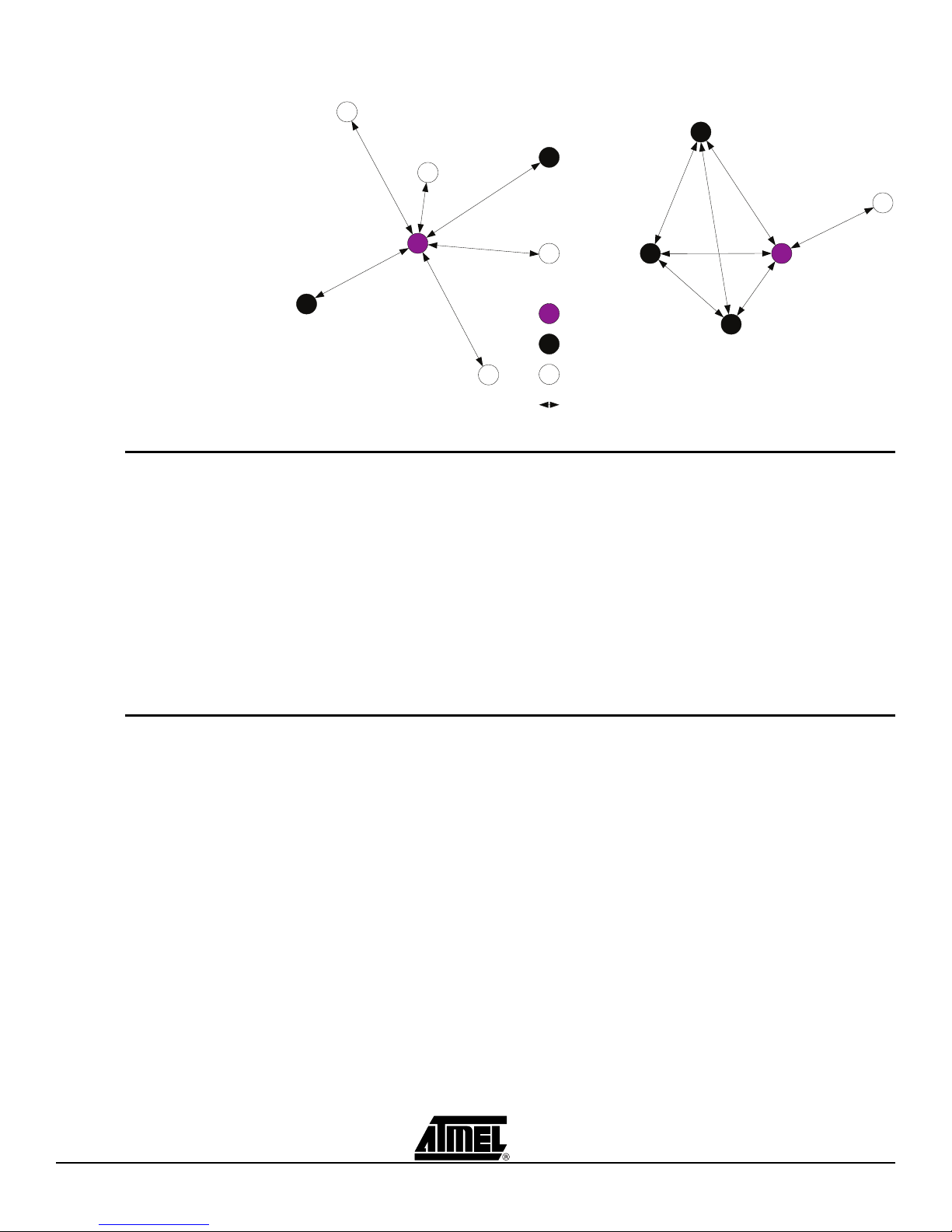
Figure 1-1. Star and peer-to-peer topology examples
Star Topology
PAN Coordinator
Full Function Device
Reduced Function Device
Communications Flow
Peer-to-Peer Topology
1.3 Demonstration
kit features
1.4 Included in the
kit
Network devices can be configured and reconfigured wirelessly from a PAN
coordinator (Display Board)
Simple application interface (pushbutton switches and LEDs)
Wide application usage
Choice of RCB application software
How to use the Atmel IEEE 802.15.4 communication-stack
Non-beacon-enabled network
IEEE 802.15.4 compliant
The kit features two component types: the Display Board and the Radio Controller
Boards (RCBs). The following items are included in the kit.
Display Board (1) with AA Batteries (2)
AT86RF230 RCBs (5) with PCB Antenna and two AAA Batteries each
CDROM containing:
– AVR Studio
–WinAVR
®
4
™
20060421
– Atmel RCB and Display Board firmware
–User Guide
AVRISP mkII In-System Programmer (Used for programming firmware)
AC Adaptor furnishing 3V (used to power the Display Board only)
1-2 Demonstration Kit User Guide
5183A–ZIGB–12/07/06
Page 7

Section 2 Getting Started
This section provides brief instructions to get the Demonstration kit up and running in
the shortest amount of time. Persons reading this section should be familiar with wireless networking; otherwise, read section 3 and section 4 for a full description of the
Demonstration kit. This Demonstration kit is fully self-contained, no external hardware
or software is required to conduct the network demonstration. However, in the event
RCB or Display board reprogramming is desired, a PC is required.
2.1 Hardware
assembly
2.2 Starting and
using the
network
The hardware is assembled by following the steps listed below. Pictures with itemized
callouts are shown in Section 3.
1. Assemble the five RCBs by inserting two AAA batteries.
2. Assemble the Display Board by inserting two AA batteris at the bottom of the
board and connecting any RCB.
Network device activity is monitored in two places: the network monitor screen and on
the RCBs designated LED units. The following steps describe device monitoring and
the reconfiguration of network devices over the wireless link.
For more detailed information about the following steps, see Section 5, running the
demonstration.
1. On the Display Board, move the power switch toward the edge of the board
(BAT).
2. When the Atmel splash screen is displayed, move the power switch on the
attached RCB away from the antenna to the ON position.
3. Observe the LCD display indicate channel scan.
4. One at a time, sequentially turn on the four remaining RCBs.
5. Observe as the devices associate with the PAN coordinator (Display) and
populate the Configure screen on the LCD.
6. After all the RCBs are associated, press the SW1 button on the Display
Board to switch to the network monitor screen.
7. Locate the RCBs associated as Switches by checking the MAC address
shown on the Network Monitor screen with the MAC address printed on the
labels attached to each RCB. Observe the LED illumination on an RCB des-
ignated as an LED Unit and also the count increment in the network monitor
screen.
8. Press SW1 to return to the Configure screen.
Note: In the following steps, at a minimum, one RCB must be assigned the function of
a Switch Unit and one RCB must be assigned the function of an LED Unit.
Demonstration Kit User Guide 2-1
5183A–ZIGB–12/07/06
Page 8

9. Randomly change the functionality of the RCBs in the Configure screen by
first selecting the desired unit by pressing the joystick up or down, then press
SW2 to change the function to either an LED unit or one of the three switch
units.
10. Press SW1 to return to Network Monitor mode and observe the new function
of the units.
11. When finished, return all power switches to the OFF position.
12. Please consult Table 7-1 if problems are encountered.
13. RCBs must contain a valid MAC address. If the MAC address was reset to
FF-FF-FF-FF-FF-FF-FF-FF you must reprogram the MAC address as outlined in section 6.2.3..
2-2 Demonstration Kit User Guide
5183A–ZIGB–12/07/06
Page 9
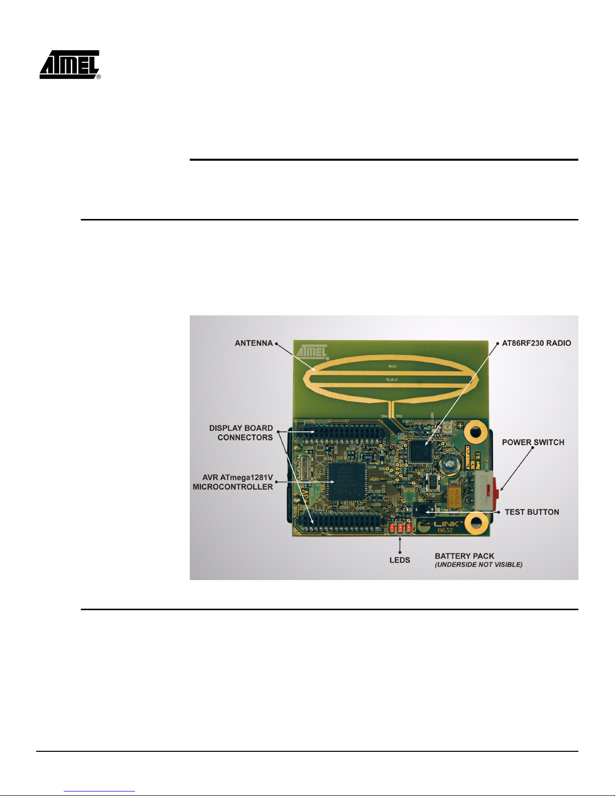
Section 3 Hardware Description
This section contains a description of the hardware furnished with the Demonstration
Kit.
3.1 Z-Link RCBs The five RCBs are identical and each contains a radio and microcontroller. The micro-
controller contains the application firmware needed to run the demonstration. This
aplication is linked to the MAC (Medium Access Control), PHY, and HAL layers that
communicate with the AT86FR230.
The key components of the RCB are shown in Figure 3-1.
Figure 3-1. Key Components of the RCB
3.2 Display Board The Display Board is used to configure and monitor the network devices. Key compo-
nents of the Display Board are shown in Figure 3-2. An RCB mounted on the Display
Board is shown in Figure 3-3, and the connectors on the Display Board are shown in
Figure 3-4.
Demonstration Kit User Guide 3-1
5183A–ZIGB–12/07/06
Page 10

Figure 3-2. Key Components of the Display Board
Figure 3-3. RCB Mounted on the Display Board
3-2 Demonstration Kit User Guide
5183A–ZIGB–12/07/06
Page 11

Figure 3-4. Display Board connectors
Demonstration Kit User Guide 3-3
5183A–ZIGB–12/07/06
Page 12

3-2 Demonstration Kit User Guide
5183A–ZIGB–12/07/06
Page 13

Section 4 Functional Overview
This section describes how the software furnished with the kit is used to demonstrate a
simple IEEE 802.15.4 network operating with a star topology. The star network is
shown below in Figure-4.1 and consists of a Personal Area Network (PAN) Coordinator
and a number of End Devices (in the case of this kit). The distinguishing feature of a
star network topology is that communication between End Devices is always routed
through the PAN Coordinator. Direct communication between End Devices is never
allowed.
Figure 4-1. Simple star network
4.1 Channel Scan
PAN Coordinator
End Device
The process of creating a network begins with the PAN Coordinator. Upon power up,
the PAN Coordinator must select a channel on which to create its network. The PAN
Coordinator does this by broadcasting a Beacon Request message. The PAN Coordinator repeats this broadcast on all channels from 11 to 26 in search of a channel without
a PAN Coordinator. If the channel is in use by another network, that network’s PAN
Coordinator will respond with a Beacon. However, if the channel is unoccupied, the
Beacon Request will not be answered. By default, the lowest unoccupied channel of the
scan becomes the channel on which the network will form.
Demonstration Kit User Guide 4-1
5183A–ZIGB–12/07/06
Page 14

4.2 End Device
Association &
Network
Configuration
As each End Device is turned on, it performs an active scan of all channels from 11 to
26, broadcasting a Beacon Request and recording all information that it receives from all
PAN Coordinator beacons. The End Device will then select the channel that corresponds to the PAN Coordinator with the correct PAN ID value that it is searching for.
The End Device will attempt to “associate” to the PAS Coordinator. Sucessful association will result in a network address assignment to the End Device. By default, the
software in this kit assigns the first associated End Device the function of LED (output),
the second associated End Device the function of Switch 1 (input), the third – Switch 2,
and the fourth – Switch 3. Pressing SW1 on the PAN Coordinator completes the configuration of the network and allows the End Devices to operate as defined.
4.3 Network
Operation
Now that the network configuration is complete, pressing the pushbutton switch (T1) on
the End Device corresponding to Switch 1 will send a message to the PAN Coordinator
to notify the End Device corresponding to LED, D1, to toggle its state. Similarly, End
Devices corresponding to Switches 2 and 3 control LEDs D2 and D3 respectively. Additional End Device information is captured and displayed on the LCD screen during
normal network operation. This includes the total number of times Switch 1, 2, and 3
were pressed, the power level in dBm of the received packet betwen the End Device
and the PAN, as well as the current state of each LED. Additional details with regard to
changing the network configuration are described in the next section.
4-2 Demonstration Kit User Guide
5183A–ZIGB–12/07/06
Page 15

Section 5 Running the
Demonstration
The Demonstration Kit consists of five RCB nodes, one of which is connected into the
Display Board and will act as a PAN Coordinator. Starting the network and experimenting with network reconfiguration are discussed in the following subparagraphs.
Note: The following paragraph discusses starting the network with the PAN Coordina-
tor started first and then the nodes coming online in random sequence. The
network can also be started with the nodes being started first and then the PAN
Coordinator coming online and establishing the network. A combination of
these two approaches can also be used.
5.1 Starting the
network
After the RCB is connected to the Display Board, the power switch on the Display Board
should be moved to BAT for battery power, or EXT for AC Adaptor power. The Atmel
splash screen is displayed on the LCD display similar to that shown in Figure 5-1.
Figure 5-1. Atmel splash screen
Note: While the Display Board can be powered from an ac adaptor or batteries, all of
the RCBs must have batteries installed.
While the splash screen is displayed, move the power switch on the attached RCB to
ON (towards the LCD screen). The RCB will then scan all channels in the 2450 MHz
band - Channels 11 (2405 MHz) through 26 (2480 MHz) for other active PANs. The display during channel scan is shown in Figure 5-2.
Figure 5-2. Screen during Channel scan
The RCB firmware will determine if a PAN exists on each channel and select the lowest
channel where there is no conflicting PAN. When a channel is selected (11 in this case),
the display will be similar to Figure 5-3.
Demonstration Kit User Guide 5-1
5183A–ZIGB–12/07/06
Page 16
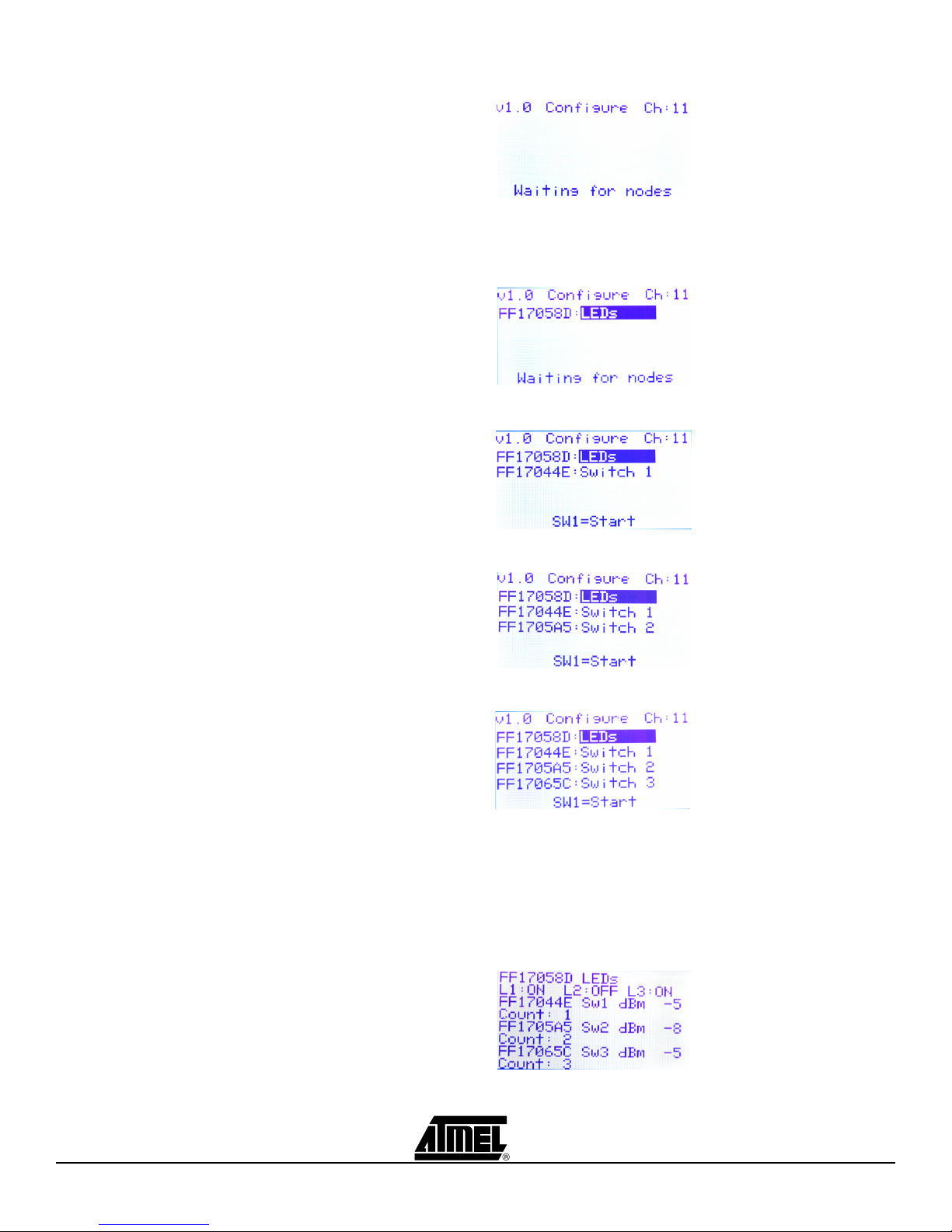
Figure 5-3. Channel selected and waiting for nodes.
The four remaining RCBs can now be powered on in random order. Figure 5-4 through
Figure 5-7 shows the Configure screen as the nodes are powered on.
Figure 5-4. First device found, assign as LED
Figure 5-5. Second device found, and assigned as Switch 1 (Toggles LED1)
Figure 5-6. Third device found, and assigned as Switch 2 (Toggles LED2)
Figure 5-7. Fourth device found, and assigned as Switch 3 (Toggles LED3)
The Configure screen is used to reconfigure the network nodes. After the nodes have
been configured in this screen, SW1 toggles the display between the Configure screen
and the Network Monitor screen shown in Figure 5-8.
Figure 5-8. Network monitor screen
5-2 Demonstration Kit User Guide
5183A–ZIGB–12/07/06
Page 17
5.2 Reconfiguring
the network
All configurations of the network nodes are performed in the Configure screen on the
Display Board.
Note: This demonstration requires at least two nodes to associate with the PAN Coor-
dinator. This is because the demonstration expects a minimum of one LED
device and one switch device.
With the Configure screen displayed, the functions of the device can be changed by
using the joystick to highlight the device’s existing function. When the function is highlighted, pressing SW2 will cycle between the available options (Switch or LEDs).
Consult Figure 5-4 through Figure 5-7 and their captions.
The switch functions on the Display Board are shown below.
SW1: Toggles the display between the Configure screen (Figure 5-7) and the
Network Monitor screen (Figure 5-8).
SW2:
1. When the Configure screen (Figure 5-7) is displayed, pressing this button
changes the highlighted function of the device. The functions are:
–LED
– Switch 1
– Switch 2
– Switch 3
5.3 Using the
network
Joystick: The joystick up and down switch are used to highlight the device function on
the Configure screen (Figure 5-7).
Joystick Push: By pressing down on the joystick, the PAN Coordinator will attempt to
communicate to all devices. If any devices are out of range or become disassociated,
they will be removed from the network table.
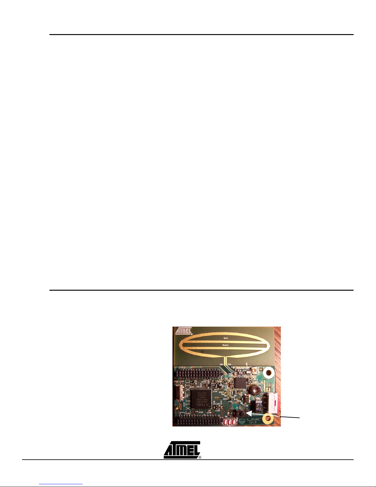
Each RCB has a Test button and three LEDs. Figure 5-9 shows an RCB with all three
LED’s illuminated:
Figure 5-9. RCB Test button
Demonstration Kit User Guide 5-3
RCB Test button
5183A–ZIGB–12/07/06
Page 18

Each RCB configured as an LED unit will show the state of the switch device’s value (on
or off). The value of the LEDs will also be shown on the Display Board in the network
monitor screen. The LEDs are disabled on devices configured as switch devices. If an
RCB is configured as an LED unit and has gone out of range, a message “Device out of
Range” will be displayed for the associated device.
When a switch device’s Test button is pressed, a data frame is constructed and the
device’s MAC transmits the frame to the PAN coordinator. When the PAN coordinator
receives the frame (data indication) it updates (toggles) the state of the LED associated
with the switch device. The data representing the new state of the LEDs is transmitted to
all devices that are configured for LEDs. When the LED device receives the dataframe it
updates its internal record of LED states, displays the state on the physical LEDs and
the transaction is finished. If a switch device goes out of range from the PAN Coordinator, the center LED will flash briefly to notify that it is out of range.
The Network Monitor screen will always reflect the current state of the LEDs on the LED
devices as well as a running sum of the button pushes for each of the switch devices.
This running sum count will be cleared after leaving the network monitor mode.
5-4 Demonstration Kit User Guide
5183A–ZIGB–12/07/06
Page 19
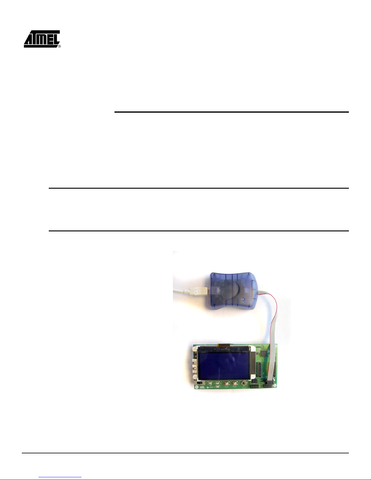
Section 6 Re-programming Display
and RCB Firmware
This demonstration kit includes resources needed to reprogram the RCB Firmware.
The following paragraphs overview the installation and use of the Atmel AVRISP mkII
In-system Programmer.
The AVRISP and JTAGICE are other tools supplied by Atmel that can be used for programming the RCBs. If the STK500 ISP port is used, be sure to remove the VTARGET
jumper. This should be done to prevent voltage conflicts between the STK500 platform
and RCB.
6.1 Atmel AVR
Studio
installation
6.2 Overview of the
programming
process
Double click on the AVR Studio installer included on the CD. Atmel recommends that
you accept the default installation parameters.
Both the Display Board firmware and the RCB firmware are imaged through the Display
Board using the AVRISP mkII In-System Programmer.
Figure 6-1. Display Board Layout
Demonstration Kit User Guide 6-1
5183A–ZIGB–12/07/06
Page 20

6.2.1 Programming the
Display Board
The following steps show how to re-program the ATmega128 microcontroller located on
the Display Board.
Remove RCB from Display board.
1. Connect the 6-pin cable from the AVRISP mkII to the Display ISP connector
(upper right) on the Display Board. Verify that the Display Board is powered on.
2. Start AVR Studio. From the Tools menu, select Program AVR, and select Connect. Choose AVRISP mkII from the list of platforms and the port where it is
connected. Press the Connect button. The AVRISP mkII programming window
should now be visible.” Note space between ‘AVR’ and ‘Studio’.
3. In the Program tab, select the target Device as ATmega128.
4. Ensure that the following fuse settings are selected using AVR Studio in the
Fuses tab:
– JTAG Interface Enabled; [JTAGEN=0]
– Preserve EEPROM memory through the Chip Erase cycle; [EESAVE=0]
– Preserve EEPROM memory through chip erase cycle. [EESAVE=0]
– Boot programming section size=4096 words Boot start address=$F000;
[BOOTSZ=00]; default value
– Brown-out detection level at VCC=2.7V; [BODLEVEL=1]
– Int. RC Osc. 8 MHz; Start-up time: 6 CK + 4ms; [CKSEL=0100 SUT=01]”.
– The final fuse value written is 0xFF, 0x91, 0xD4.
5. Go back to the Program tab, in the Flash section, browse to the location of the
input HEX file and select the filename: rz200_display_board_v1_0.hex. Press
Program and verify that the process terminates successfully.
6. Alternatively, fuse settings can be altered using JTAG ICE mkII. In this case,
the Serial program downloading (SPI) enabled; [SPIEN=0] fuse must be
checked.
6.2.2 Programming the
RCB
The following steps show how to re-program the ATmega1281 microcontroller located
on the RCBs.
1. Connect RCB to the Display board. Connect the 6-pin cable from the AVRISP
mkII to the RCB ISP connector (upper left) on the Display Board. Verify that the
RCB is powered on (move the switch away from the antenna).
2. Start AVR Studio. From the Tools menu, select Program AVR, and select Connect. Choose AVRISP mkII from the list of platforms and the port where it is
connected. Press the Connect button. The AVRISP mkII programming window
should now be visible.
3. In the Program tab, select the target Device as ATmega1281.
4. Ensure that the following fuse settings are selected in the Fuses tab:
– Brown-out detection disabled; [BODLEVEL=111]
– JTAG Interface Enabled; [JTAGEN=0]
– Preserve EEPROM memory through chip erase cycle. [EESAVE=0]
– Boot program section size=4096 words Boot start address=$F000;
[BOOTSZ=00]; default value
– Int. RC Osc. 8 MHz; Start-up time: 6 CK + 65ms; [CKSEL=0100 SUT=01]
– The final fuse value written is 0xFF, 0x91, 0xE2.
6-2 Demonstration Kit User Guide
5183A–ZIGB–12/07/06
Page 21

5. Go back to the Program tab, in the Flash section, browse to the location of the
input HEX file and select the filename: rz200_v1_0.hex. Press Program and verify that the process terminates successfully.
6. Alternatively, fuse settings can be altered using JTAG ICE mkII. In this case,
the Serial program downloading (SPI) enabled; [SPIEN=0] fuse must be
checked.
6.2.3 How to re-program
the RCB MAC
address
The 64-bit IEEE MAC address associated with the RCB is stored in the internal
EEPROM of the ATmega1281 that is on the RCB at address 0 (LSB). If the MAC
address has been inadvertently erased, the following steps can be followed to reprogram it into the EEPROM. This procedure should not be attempted if the RCB has a
valid MAC address. The following steps can only be performed with the JTAGICE mkII
while AVRStudio is running in Debug mode. This operation cannot be performed with
the AVRISP mkII included in your Demonstration kit.
The following steps reprogram the MAC address and MUST be completed from start to
finish once the program memory has been loaded (step 4), otherwise the RCB’s MAC
address will be overwritten with all FFs.
1. Open AVR Studio.
2. Connect the JTAGICE mkII to the RCB programming header located on the Display Board.
3. From the File Menu, select Open File and open the file rz200_v1_0.hex from the
CDROM.
4. In the Save AVR Studio Project File dialog box, select Save to create a project
file.
5. In the Select Device and Debug Platform dialog box, select JTAGICE mkII as the
debug platform, ATmega1281 as the device, and then select Finish to start the
AVR Studio disassembler and load the program memory.
6. Enter drop menu Debug -> JTAGICE mkII Options
7. Select Debug tag
8. In the General area, select the ‘Preserve EEPROM contents when reprogramming device’ box and hit OK.
9. If the EEPROM Memory window is not already open: from the View tab, open
the active HEX file’s EEPROM contents by selecting EEPROM from the Memory
Window drop down list. The EEPROM memory window should contain all FF’s.
10. Starting at location 0 (the upper most left corner of the window), enter the 16
byte MAC address printed on the back of the RCB PCB in reverse order.
Note: The MAC address MUST be written in reverse order in 2 byte pairs, i.e., if the
MAC address is 00-04-25-FF-FF-17-01-52, the sequence written into the
EEPROM must be entered as 52-01-17-FF-FF-25-04-00 from location 0. The
MAC address will automatically be saved to the EEPROM with each keystroke.
11. From the Project tab, select Close Project. You will be prompted to close and
end the debug session, select OK.
Caution: In the following step, you must select No. Selecting Yes will cause the MAC
address you just entered to be to permanently saved into the demokitfirmware.hex file.
This will make the file unuseable for other RCBs.
12. You will then be prompted to save the changes to demokitfirmware.hex. Select
Demonstration Kit User Guide 6-3
No.
5183A–ZIGB–12/07/06
Page 22

6-2 Demonstration Kit User Guide
5183A–ZIGB–12/07/06
Page 23
Section 7 Troubleshooting
Possible problems and their solution are shown in Figure 7-1.
Table 7-1. Troubleshooting
Problem Reason Solution
No response from any board Power Switch is OFF Ensure power switch is ON
Dead Batteries Check battery condition and replace if necessary
The LEDs on the Z-Link RCB
will not illuminate
The RCB is not configured as an
LED Unit
Power Switch is OFF Ensure power switch is ON
Dead Batteries Check battery condition and replace if necessary
Check configuration. Only the LEDs on an LED Unit will
illuminate.
The Test Button does nothing The RCB is not configured as a
Switch Unit
Power Switch is OFF Ensure power switch is ON
Dead Batteries Check battery condition and replace if necessary
The configuration shown in
the Configure screen is not
transmitted to the network
nodes
The Test Button does not
work
The middle LED on the RCB
blinks when I press the Test
Button
RCB lights stay on and the
node will not show up in the
Configure screen
RCB is not attached to the Display
Board
Network nodes are out of range Bring network nodes back into range of the Coordinator
The RCB batteries are dead Replace batteries
The RCB is out range to the
Coordinator and the Coordinator is
not receiving any packets from the
RCB
The Coordinator has lost power
since going into the Network Monitor
mode
The RCB will not associate if it loses
its MAC address
Check configuration. Only the Test Buttons on a Switch Unit
are active and should illuminate an LED on an LED Unit
Ensure that the RCB is attached to the Display Board
Go back into the range of the Coordinator
Ensure power switch on Coordinator is ON, or check
Coordinator battery condition and replace if necessary
Reprogram your MAC address (see section 6.2.3)
Demonstration Kit User Guide 7-1
5183A–ZIGB–12/07/06
Page 24

7-2 Demonstration Kit User Guide
5183A–ZIGB–12/07/06
Page 25

Atmel Corporation Atmel Operations
2325 Orchard Parkway
San Jose, CA 95131, USA
Tel: 1(408) 441-0311
Fax: 1(408) 487-2600
Regional Headquarters
Europe
Atmel Sarl
Route des Arsenaux 41
Case Postale 80
CH-1705 Fribourg
Switzerland
Tel: (41) 26-426-5555
Fax: (41) 26-426-5500
Asia
Room 1219
Chinachem Golden Plaza
77 Mody Road Tsimshatsui
East Kowloon
Hong Kong
Tel: (852) 2721-9778
Fax: (852) 2722-1369
Japan
9F, Tonetsu Shinkawa Bldg.
1-24-8 Shinkawa
Chuo-ku, Tokyo 104-0033
Japan
Tel: (81) 3-3523-3551
Fax: (81) 3-3523-7581
Memory
2325 Orchard Parkway
San Jose, CA 95131, USA
Tel: 1(408) 441-0311
Fax: 1(408) 436-4314
Microcontrollers
2325 Orchard Parkway
San Jose, CA 95131, USA
Tel: 1(408) 441-0311
Fax: 1(408) 436-4314
La Chantrerie
BP 70602
44306 Nantes Cedex 3, France
Tel: (33) 2-40-18-18-18
Fax: (33) 2-40-18-19-60
ASIC/ASSP/Smart Cards
Zone Industrielle
13106 Rousset Cedex, France
Tel: (33) 4-42-53-60-00
Fax: (33) 4-42-53-60-01
1150 East Cheyenne Mtn. Blvd.
Colorado Springs, CO 80906, USA
Tel: 1(719) 576-3300
Fax: 1(719) 540-1759
Scottish Enterprise Technology Park
Maxwell Building
East Kilbride G75 0QR, Scotland
Tel: (44) 1355-803-000
Fax: (44) 1355-242-743
RF/Automotive
Theresienstrasse 2
Postfach 3535
74025 Heilbronn, Germany
Tel: (49) 71-31-67-0
Fax: (49) 71-31-67-2340
1150 East Cheyenne Mtn. Blvd.
Colorado Springs, CO 80906, USA
Tel: 1(719) 576-3300
Fax: 1(719) 540-1759
Biometrics/Imaging/Hi-Rel MPU/
High Speed Converters/RF Datacom
Avenue de Rochepleine
BP 123
38521 Saint-Egreve Cedex, France
Tel: (33) 4-76-58-30-00
Fax: (33) 4-76-58-34-80
Disclaimer: The information in this document is provided in connection with Atmel products. No license, express or implied, by estoppel or otherwise, to any
intellectual property right is granted by this document or in connection with the sale of Atmel products. EXCEPT AS SET FORTH IN ATMEL’S TERMS AND CONDI-
TIONS OF SALE LOCATED ON ATMEL’S WEB SITE, ATMEL ASSUMES NO LIABILITY WHATSOEVER AND DISCLAIMS ANY EXPRESS, IMPLIED OR STATUTORY
WARRANTY RELATING TO ITS PRODUCTS INCLUDING, BUT NOT LIMITED TO, THE IMPLIED WARRANTY OF MERCHANTABILITY, FITNESS FOR A PARTICULAR
PURPOSE, OR NON-INFRINGEMENT. IN NO EVENT SHALL ATMEL BE LIABLE FOR ANY DIRECT, INDIRECT, CONSEQUENTIAL, PUNITIVE, SPECIAL OR INCIDENTAL DAMAGES (INCLUDING, WITHOUT LIMITATION, DAMAGES FOR LOSS OF PROFITS, BUSINESS INTERRUPTION, OR LOSS OF INFORMATION) ARISING OUT
OF THE USE OR INABILITY TO USE THIS DOCUMENT, EVEN IF ATMEL HAS BEEN ADVISED OF THE POSSIBILITY OF SUCH DAMAGES. Atmel makes no
representations or warranties with respect to the accuracy or completeness of the contents of this document and reserves the right to make changes to specifications
and product descriptions at any time without notice. Atmel does not make any commitment to update the information contained herein. Unless specifically provided
otherwise, Atmel products are not suitable for, and shall not be used in, automotive applications. Atmel’s products are not intended, authorized, or warranted for use
as components in applications intended to support or sustain life.
©2006 Atmel Corporation. All rights reserved. Atmel®, logo and combinations thereof, Everywhere You Are®, AVR® and others, are registered
trademarks, Z-Link
others.
™
and others are trademarks of Atmel Corporation or its subsidiaries. Other terms and product names may be trademarks of
Literature Requests
www.atmel.com/literature
Printed on recycled paper.
5183A–ZIGB–12/07/06
Page 26

Mouser Electronics
Authorized Distributor
Click to View Pricing, Inventory, Delivery & Lifecycle Information:
Atmel:
ATAVRRZ200 ATAVRRZ201
 Loading...