


Features
• Power Management
– Supply Input from USB or 1x Disposal Battery (Alkaline, NimH, NiCd)
– Input Voltage Range: 0.9V to 1.8V
– 2.7V/2.9V/3.1V/3.3V - 100 mA Step-Up DC/DC Converter for Main Supply
– 2.7V to 3.5V (100mV step) - 150 mA LDO from USB supply
– 2.4V to 3.0V (200mV step) - 60 mA LDO for Analog Supply
– Reset Generator
– SPI Interface and Internal Programming Registers
– Dynamic Power Management
– Very Low Quiescent Current Operation
• Stereo Audio DAC
– Programmable Stereo Audio DAC (16-bits, 18-bits or 20-bits)
– 93 dB SNR Playback Stereo Channels
– 32 Ohm/20 mW Stereo Headset Drivers with Master Volume and Mute Controls
– Stereo Line Level Input with Volume Control/Mute and Playback through the
Headset Driver
– Microphone Preamplifier
– Stereo, Mono and Reverse Stereo Mixer
– Left/Right Speaker Short-Circuit Detection Flag
– 8, 11.024, 16, 22.05, 24, 32, 44.1 and 48 kHz Sampling Rates
– 256x or 384xFs Master Clock Frequency
– I2S Serial Audio Interface
– Low Power Operation
• Applications:
– Ideally Suited to Interface with Atmel’s AT8xC51SNDxC MP3 Microcontroller
– Portable Music Players, Digital Cameras, CD Players, Handheld GPS
Power
Management
and Analog
Companions
(PMAAC)
AT73C209
Audio and Power
Management
1. Description
The AT73C209 is a fully integrated, low cost, combined Stereo Audio DAC and Power
Management Circuit targeted for battery powered devices such as MP3 players in
“walkman” format or “mass storage” USB format.
The stereo DAC section is a complete high performance, stereo audio digital-to-analog converter delivering a 93 dB dynamic range. It comprises a multibit sigma-delta
modulator with dither, continuous time analog filters and analog output drive circuitry.
This architecture provides a high insensitivity to clock jitter. The digital interpolation filter increases the sample rate by a factor of 8, using 3 linear phase half-band
cascaded filters, followed by a first order SINC interpolator with a sample-rate factor of
8. This filter eliminates the images of baseband audio, retaining only the image at 64x
the input sample rate, which is eliminated by the analog post filter. Optionally, a dither
signal can be added that reduces possible noise tones at the output. However, the
use of a multibit sigma-delta modulator provides extremely low noise tone energy.
Master clock is 256 or 384 times the input data rate, allowing multiple choice of input
data rate up to 48 kHz, including standard audio rates of 48, 44.1, 32, 16 and 8 kHz.
The DAC section also comprises volume and mute control and can be simultaneously
played back directly on the line outputs and through a 32-Ohms stereo headset.
6365A–PMAAC–12-Mar-08

The 32-Ohms pair of stereo-headset drivers also includes a LINEL and LINER channel-mixer
pair of stereo inputs.
Every DAC can be powered down separately via internal register control. Each single left or right
DAC can be directed in MONO mode to the stereo headset and line outputs while the other is
set in off mode.
In addition, a microphone preamplifier with a microphone bias switch is integrated, reducing
external ICs and saving board space.
The volume, mute, power down, de-emphasis controls and 16-bit, 18-bit and 20-bit audio formats are digitally programmable via a 4-wire SPI bus and the digital audio data is provided
through a multi-format I2S interface.
The Power Management section can tolerate several types of input supply, such as:
• Battery: voltage is converted to 3.3V via a DC/DC step up converter using 1 external inductor,
1 schottky diode and a capacitor.
– Disposable AA or AAA size
– coin cell size, 1 cell, as low as 0.9V for alkaline
• USB: 5V VBUS supply from a USB connector or a Lithium-Ion battery
The Power Management section also includes a set of low dropout (LDO) voltage regulators
with different voltages to supply specific chip and analog requirements:
• LDO1 is designed to drive up to 150 mA from a USB port with 9-step programmable output
voltages: 2.7V, 2.8V, 2.9V, 3.0V, 3.1V, 3.2V, 3.3V, 3.4V, 3.5V. Default voltage is 3.4V and
represents the initial output voltage of LDO1 at start up. When RSTB is activated, the
external MCU can change the output voltage via the SPI serial interface. This LDO is
designed to supply the complete chip when the device is connected to a USB port.
• LDO2 is designed to drive up to 60 mA from LDO1 with 4-step programmable output
voltages: 2.4V, 2.6V, 2.8V, 3.0V with low noise and high PSRR. Default voltage is 3.0V and
represents the initial output voltage of LDO2 at start up. When RSTB is activated, the MCU
can change the output voltage via the SPI serial interface. This LDO is designed to supply the
internal analog section.
2
AT73C209
6365A–PMAAC–12-Mar-08
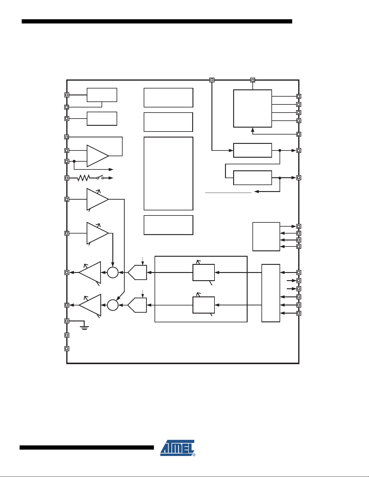
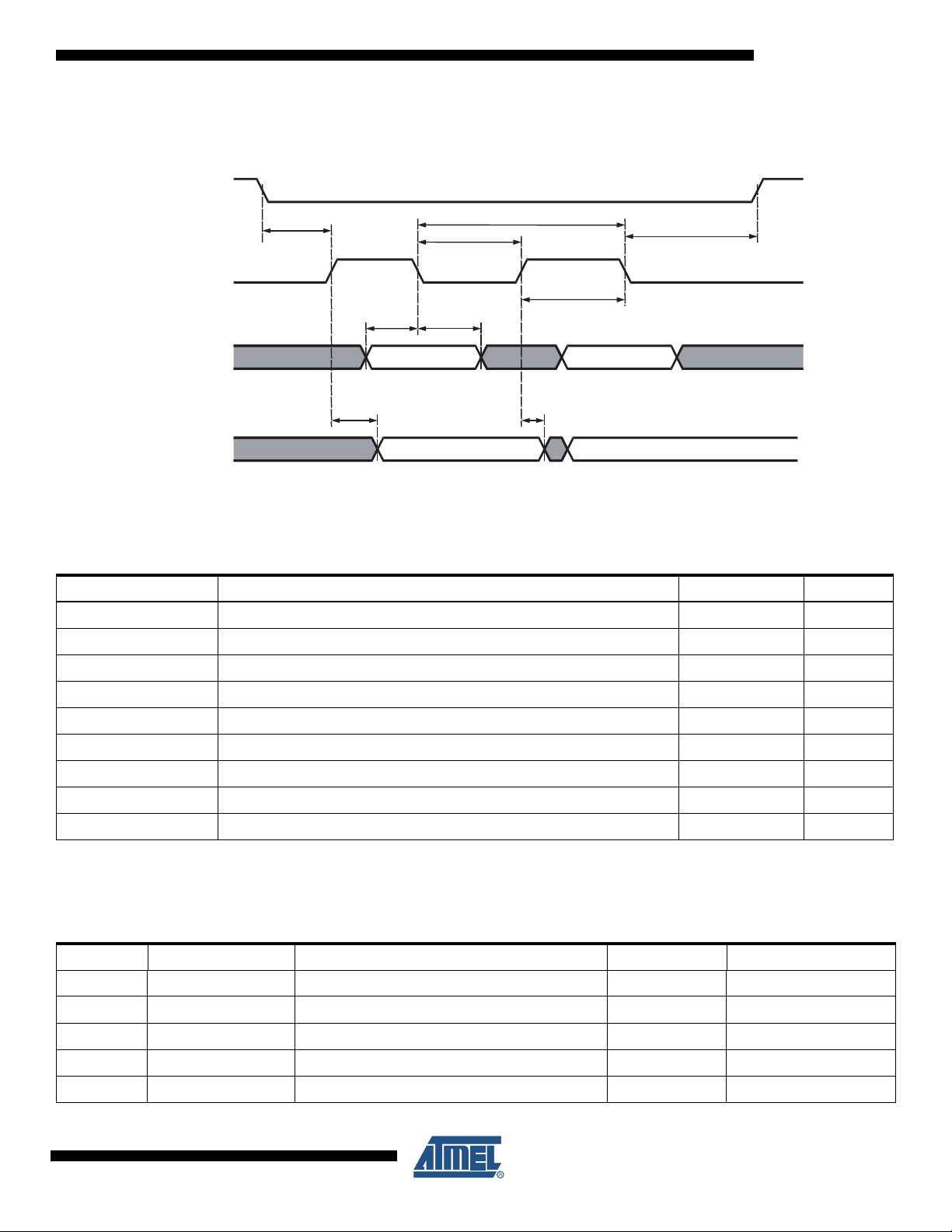
2. Block Diagram
Figure 2-1. AT73C209 Functional Block Diagram
AT73C209
INUSB
VREF
GNDB
VBG
MICOUT
MICINN
VCM
MICB
LINEL
LINER
HSR
HSL
INGND
Voltage
Reference
Band
Gap
PGA
PGA
-36 to +12dB/
3dB step
PGA
-36 to +12dB/
3dB step
PGA
-6 to +6dB/ 3dB step
32Ω
Driver
-6 to +6dB/ 3dB step
32Ω
Driver
Internal VCM
to LDO2
Σ
Σ
Power Management
en_DAR
DAC
en_DAL
DAC
Integrated RC
Oscillator
Temperature
Monitoring Unit
Logic
Status
Registers
-46.5dB to 0dB
1.5dB step
-46.5dB to 0dB
1.5dB step
SW1
DC-DC Step Up
3.3V / 100mA
LDO1
3.4V / 150mA
LDO2
3.0V / 60mA
Internal Analog Section
AT73C209
Right
Volume
Control
Codec &
Mixer
Left
Volume
Control
SPI
Serial Audio I/F
LX
FB
GNDSW1
GNDSW1S
ONOFF
VBOOST
VANA
SPI_DOUT
SPI_DIN
SPI_CLK
SPI_CSB
MCLK
RSTB
ITB
SDIN
LRFS
BCLK
AVDDHS
AGNDHS
6365A–PMAAC–12-Mar-08
3
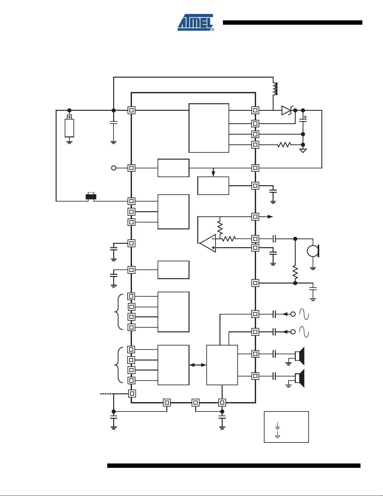
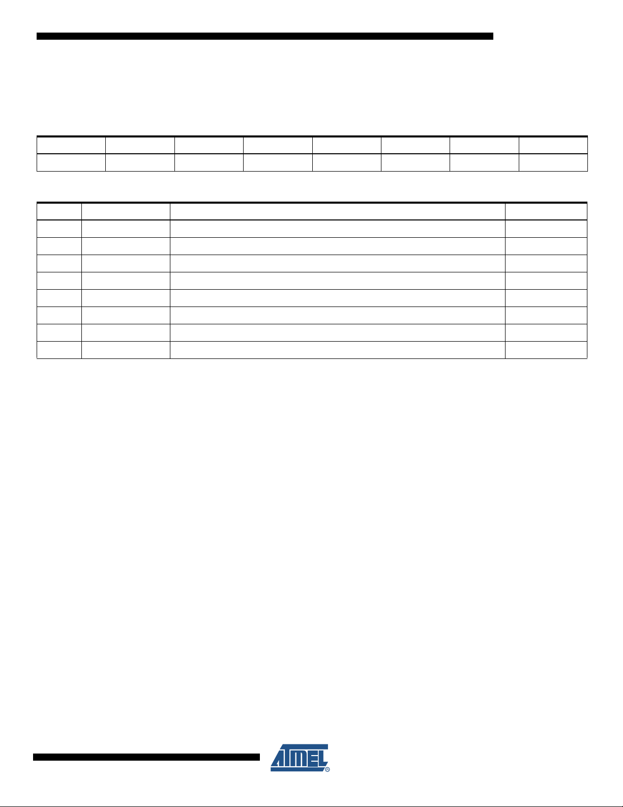
3. Application Diagram
Figure 3-1. Application Using One Cell Battery
28
0.9V to 1.8V
Battery
Cell
C14
22µF
IN
AC73C209
DC-DC
GNDSW1
GNDSW1S
LX
FB
L1
100m
R1
D1
C1
22µF
Ω
25
26
23
24
3.1V to 5.5V
Push Button
SERIAL
INTERFACE
DIGITAL
AUDIO
INTERFACE
Connected to
VANA
C10
10µF
100nF
C8
29
27
22
5
16
32
1
2
3
4
18
19
20
21
12
USB
ONOFF
RSTB
ITB
INGND
VBG
SPI_DIN
SPI_DOUT
SPI_CLK
SPI_CSB
SDIN
BCLK
MCLK
LRFS
AVDDHS
LDO1
LOGIC
CONTROL
BANDGAP
SPI
I²S
AGNDHS
GNDB
LDO2
CODEC &
MIXER
VREF
VBOOST
VANA
MICOUT
MICINN
VCM
MICB
LINER
LINEL
HSR
HSL
30
31
C2
2.2µF
8
TO ADC
C11
1µF
7
17
C9
1µF
R2
2.2K
C3
C4
C5
C6
Ω
C12
10µF
6
470nF
15
470nF
14
100µF
11
100µF
10
MIC
Analog
Signal
Analog
Signal
RIGHT
HEADSET
LEFT
HEADSET
C13
1µF
13
33
C7*
1µF
9
C7* =~ C3 + C4
NOTE:
= DGND
= AGND
4
AT73C209
6365A–PMAAC–12-Mar-08
AT73C209
4. Components List
Table 4-1. Components List
Reference Value Techno Size Manufacturer & Reference
C1 22 µF Tantalum Case A (AVX) or equivalent
C2 2.2 µF / 10V Ceramic 0603 C1608X5R1A225MT (TDK) or GRM188R61A225 (Murata)
C3 470 nF / 10V Ceramic 0402 C1005X5R1A474KT (TDK) or GRM155F51A474 (Murata)
C4 470 nF / 10V Ceramic 0402 C1005X5R1A474KT (TDK) or GRM155F51A474 (Murata)
C5 100 µF / 6.3V Ceramic 1210 C3225X5R0J107MT (TDK) or GRM32ER60J107 (Murata)
C6 100 µF / 6.3V Ceramic 1210 C3225X5R0J107MT (TDK) or GRM32ER60J107 (Murata)
C7 1 µF / 6.3V Ceramic 0402 C1005X5R0J105KT (TDK) or GRM155R60J105 (Murata)
C8 100 nF / 16V Ceramic 0402 C1005X5R1C104KT (TDK) or GRM155F51C104 (Murata)
C9 1 µF / 6.3V Ceramic 0402 C1005X5R0J105KT (TDK) or GRM155R60J105 (Murata)
C10 10 µF / 6.3V Ceramic 0402 C1608X5R0J106MT (TDK) or GRM188R60G106 (Murata)
C11 1 µF / 6.3V Ceramic 0402 C1005X5R0J105KT (TDK) or GRM155R60J105 (Murata)
C12 10 µF / 6.3V Ceramic 0603 C1608X5R0J106MT (TDK) or GRM188R60G106 (Murata)
C13 1 µF / 6.3V Ceramic 0402 C1005X5R0J105KT (TDK) or GRM155R60J105 (Murata)
C14 22 µF / 4V Ceramic 0805 C2012X5R0J226MT (TDK) or GRM21BR60J226 (Murata)
D1 -- Schottky MBRA120LT3 (ON Semiconductors) or equivalent
L1 10 µH /550mA 1812 NLC453232T-100K-PF (TDK) or LQH43CN100K03 (Murata)
R1 0.1 Ohms 1% -- in 0805 Case or can be made by PCB tracks
R2 2.2 kOhms 5% 0402
SW1 Push Button N/A N/A Series DSTMxx (APEM COMPONENTS) or equivalent
6365A–PMAAC–12-Mar-08
5
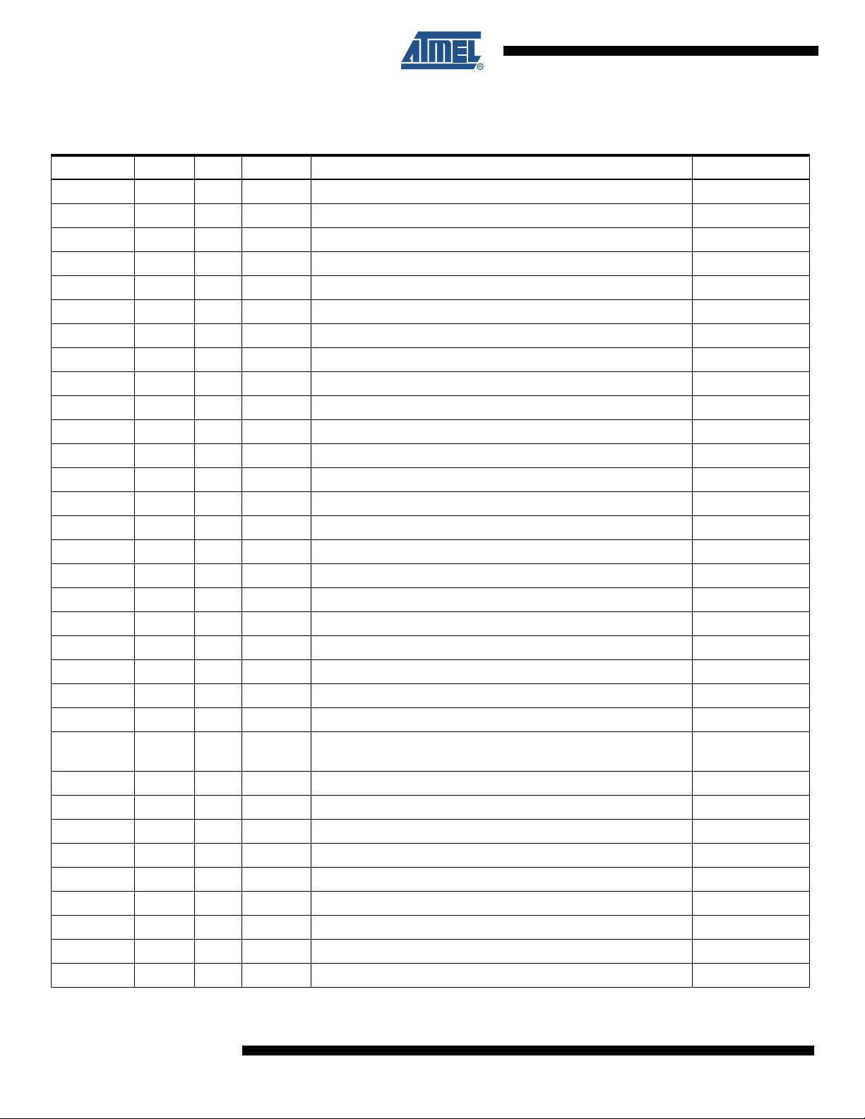
5. Pin Description
Table 5-1. Pin Description
Pin Name I/O Pin Type Function Value
SPI_DIN I 1 Digital SPI Data Input 0 - VANA
SPI_DOUT O 2 Digital SPI Data Output 0 - VANA
SPI_CLK I 3 Digital SPI Clock 0 - VANA
SPI_CSB I 4 Digital SPI Chip Select 0 - VANA
ITB O 5 Digital Open Drain Interruption / Test Analog Signal Output 0 to VANA
MICB O 6 Analog Microphone Bias --
MICINN I 7 Analog Microphone Amplifier Input Half VANA
MICOUT O 8 Analog Microphone Amplifier Output 0 to VANA
VREF O 9 Analog Voltage Reference Pin For Audio Part --
HSL O 10 Analog Line-out/Headphone Left channel output 0 - AVDDHS
HSR O 11 Analog Line-out/Headphone Right channel output 0 - AVDDHS
AVDDHS I 12 Supply Headset Amplifier Supply VANA
AGNDHS Ground 13 Ground Headset Amplifier Ground --
LINEL I 14 Analog Line-in, Left channel input --
LINER I 15 Analog Line-in, Right channel input --
INGND O 16 Analog Line-in, virtual signal ground pin for decoupling. --
VCM O 17 Analog Common Mode Reference Half VANA
SDIN I 18 Digital Serial Data Input For Audio Interface 0 - VANA
BCLK I 19 Digital Bit Clock Input For Audio Interface 0 - VANA
MCLK I 20 Digital Master Clock Input For Audio Interface 0 - VANA
LRFS I 21 Digital Audio interface left/right channel synchronization frame pulse 0 - VANA
RSTB O 22 Digital Reset Active Low Power 0 - VBOOST
GNDSW1 Ground 23 Ground SW1 Ground --
GNDSW1S I 24 Analog
LX O 25 Analog SW1 Inductor Switching Node --
FB I 26 Analog SW1 Feedback 2.7V - 3.5V
ONOFF I 27 Analog SW1 Switch On IN Level
IN I 28 Supply Input power supply voltage. Connected to single Alkaline battery 0.9V - 1.8V
USB I 29 Supply USB Supply Input 3.1 V to 5.5 V
VBOOST O 30 Analog LDO1 Output Voltage 0 to 3.5 V
VANA O 31 Analog LDO2 Output Voltage 0 to 3V
VBG O 32 Analog Band Gap Voltage
GNDB Ground 33 Ground Analog Ground --
SW1 Current Sense. Connected to 0.1 Ohms external limiting
current sense resistor
--
6
AT73C209
6365A–PMAAC–12-Mar-08
AT73C209
6. Absolute Maximum Ratings
Table 6-1. Absolute Maximum Ratings*
Operating Temperature (Industrial) -40°C to +85°C
Storage Temperature -55°C to +150°C
Power Supply Input:
on Battery Input -0.3V to +1.8V
on USB Input -0.3V to +5.5V
7. Digital IOs
All the digital IOs: SDIN, BCLK, LRFS, MCLK, RSTB, SPI_DOUT, SPI_DIN, SPI_CLK, SPI_CSB are referred to as
VBOOST.
Table 7-1. Digital IOs
Symbol Parameter Conditions VBOOST Min Max Unit
VIL Low level input voltage Guaranteed input low Voltage 2.7V to 3.5V -0.3 0.2 x VBOOST V
VIH High level input voltage Guaranteed input high Voltage 2.7V to 3.5V 0.8 x VBOOST VBOOST + 0.3 V
*NOTICE: Stresses beyond those listed under “Absolute Maximum
Ratings” may cause permanent damage to the device.
This is a stress rating only and functional operation of
the device at these or other conditions beyond those
indicated in the operational sections of this specification
is not implied. Exposure to absolute maximum rating
conditions for extended periods may affect device reliability.
VOL Low level output voltage IOL = 2 mA 2.7V to 3.5V -- 0.4 V
VOH High level output voltage IOH = 2 mA 2.7V to 3.5V VBOOST - 0.5V -- V
6365A–PMAAC–12-Mar-08
7
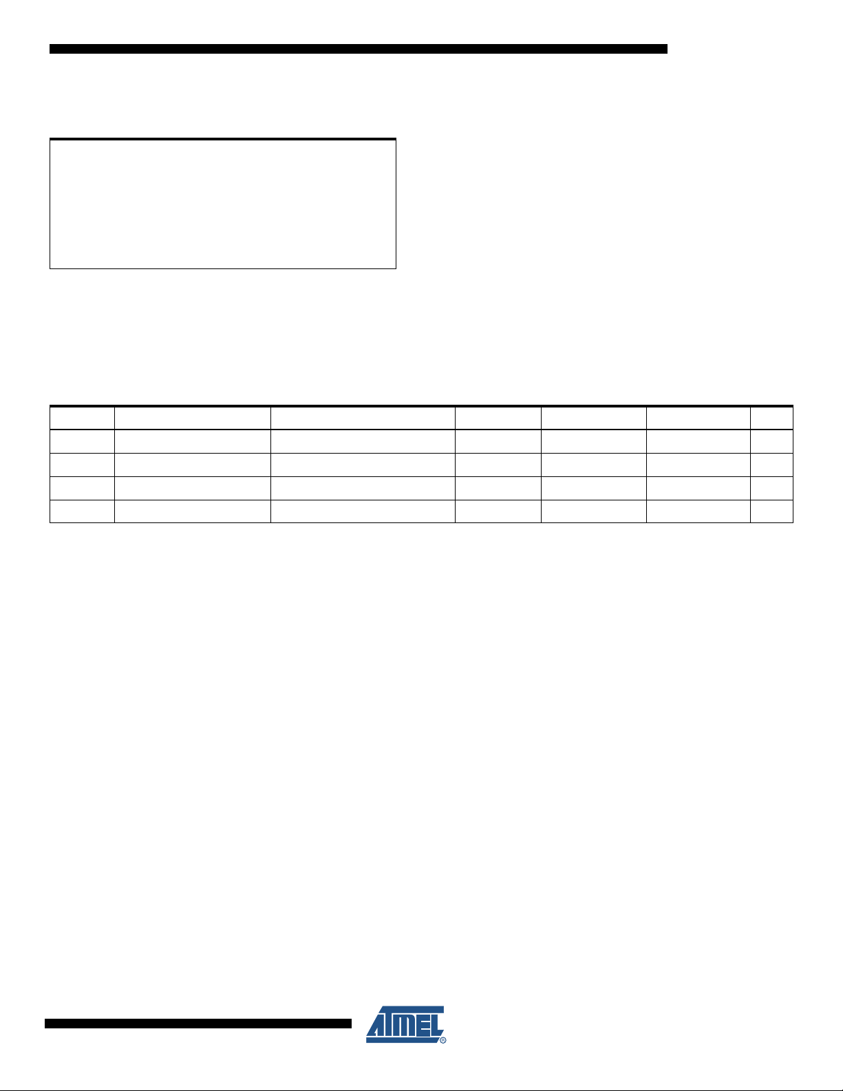
8. SPI Interface
8.1 SPI architecture
The SPI is a 4 wire bi-directional asynchronous serial link. It works only in slave mode. The protocol is the following:
Figure 8-1. SPI Protocol Diagram
SPI_CSB
8.2 SPI Protocol
SPI_CLK
d6
rw a6 a5 a4 a3 a2 a1 d7
a0
d5 d3
d4
d0
d1 d2
SPI_DIN
d7 d6 d5 d4
d2
d3
d1 d0
SPI_DOUT
On SPI_DIN, the first bit is a read/write bit. 0 indicates a write operation while 1 is for a read
operation. The 7 following bits are used for the register address and the 8 last ones are the write
data. For both address and data, the most significant bit is the first one.
In case of a read operation, SPI_DOUT provides the contents of the read register, MSB first.
The transfer is enabled by the SPI_CSB signal, active low. When there is no operation on the
SPI interface, SPI_DOUT is set in high impedance to allow sharing of MCU serial interface with
other devices. The interface is reset at every rising edge of SPI_CSB in order to return to an idle
state, even if the transfer does not succeed. The SPI is synchronized with the serial clock
SPI_CLK. Falling edge latches SPI_DIN input and rising edge shifts SPI_DOUT output bits.
Note that MCLK (Audio Interface Master Clock Input) must run during any SPI write access registers (from address 0x00 to 0x0C).
8
AT73C209
6365A–PMAAC–12-Mar-08
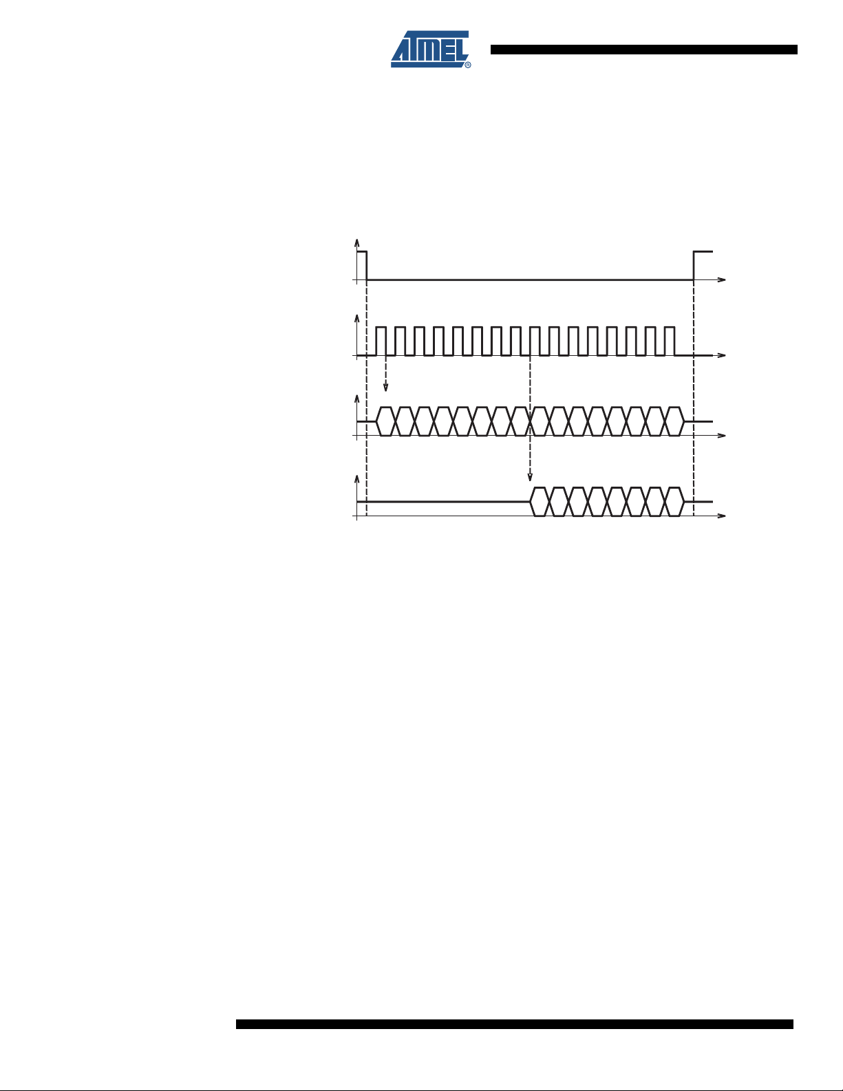
8.3 Timing Diagram for SPI Interface
Figure 8-2. SPI Timing Diagram
SPI_CSB
Tssen
SPI_CLK
Twl
Tc
AT73C209
Thsen
Twh
Tssdi
Thsdi
SPI_DIN
Tdsdo
Thsdo
SPI_DOUT
8.4 SPI Timing
Table 8-1. SPI Timing Table
Timing Parameter Description Min Max
Tc SPI_CLK min period 150 ns --
Twl SPI_CLK min pulse width low 50 ns --
Twh SPI_CLK min pulse width high 50 ns --
Tssen Setup Time SPI_CSB falling to SPI_CLK rising 50 ns --
Thsen Hold Time SPI_CLK falling to SPI_CSB rising 50 ns --
Tssdi Setup Time SPI_DIN valid to SPI_CLK falling 20 ns --
Thsdi Hold Time SPI_CLK falling to SPI_DIN not valid 20 ns --
Tdsdo Delay Time SPI_CLK rising to SPI_DOUT valid -- 20 ns
Thsdo Hold Time SPI_CLK rising to SPI_DOUT not valid 0 ns --
8.5 SPI Register Tables
Table 8-2. SPI Register Mapping
Offset Register Name Access Reset
0x00 DAC_CTRL DAC Control Read/Write 0x00
0x01 DAC_LLIG DAC Left Line in Gain Read/Write 0x05
0x02 DAC_RLIG DAC Right Line in Gain Read/Write 0x05
0x03 DAC_LPMG DAC Left Master Playback Gain Read/Write 0x08
0x04 DAC_RPMG DAC Right Master Playback Gain Read/Write 0x08
6365A–PMAAC–12-Mar-08
9

Table 8-2. SPI Register Mapping (Continued)
Offset Register Name Access Reset
0x05 DAC_LLOG DAC Left Line Out Gain Read/Write 0x00
0x06 DAC_RLOG DAC Right Line Out Gain Read/Write 0x00
0x07 DAC_OLC DAC Output Level Control Read/Write 0x22
0x08 DAC_MC DAC Mixer Control Read/Write 0x09
0x09 DAC_CSFC DAC Clock and Sampling Frequency Control Read/Write 0x00
0x0A DAC_MISC DAC Miscellaneous Read/Write 0x02
0x0C DAC_PRECH DAC Precharge Control Read/Write 0x00
0x10 DAC_RST Dac Reset Read/Write 0x00
0x11 MISC_STATUS USB and Headset Short Status Read Only 0x00
0x12 INT_MASK Interrupt Mask Read/Write 0x00
0x14 REG_CTRL Regulators Control Read/Write 0x00
0x15 SW_CTRL Switcher Control Read/Write 0x00
0x17 MIC_CTRL Microphone Amplifier Control Read/Write 0x00
0x20 DC_SEL_VOUT DC/DC Output Voltage Control Read/Write DC_SEL_VOUT = 00
10
AT73C209
6365A–PMAAC–12-Mar-08
AT73C209
8.5.1 DAC Control Register Register Name: DAC_CTRL Access Type: Read/Write Address: 0x00
76543210
RSRV1 RSRV2 ONDACR ONDACL ONLNOR ONLNOL ONLNIR ONLNIL
Register (0x00): DAC Control
Bit Name Description Reset Value
0 ONLNIL Left channel line in amplifier (L to power down, H to power up) ONLNIL = 0
1 ONLNIR Right channel line in amplifier (L to power down, H to power up) ONLNIR = 0
2 ONLNOL Left channel line out driver (L to power down, H to power up) ONLNOL = 0
3 ONLNOR Right channel line out driver (L to power down, H to power up) ONLNOR = 0
4 ONDACL Left channel DAC (L to power down, H to power up) ONDACL = 0
5 ONDACR Right channel DAC (L to power down, H to power up) ONDACR = 0
6 RSRV2 Reserved Bit 0
7 RSRV1 Reserved Bit 0
6365A–PMAAC–12-Mar-08
11
8.5.2 DAC Left Line In Gain Register Register Name: DAC_LLIG Access Type: Read/Write Address: 0x01
76543210
RSRV1 RSRV2 RSRV3 LLIG
Register (0x01): Left Line In Gain
Bit Name Description Reset Value
4:0 LLIG<4:0> Left channel line in analog gain selector LLIG<4:0>=00101 (0dB)
7:5 RSRV<1:3> Reserved Bits 000
LLIG<4:0> Gain Unit LLIG<4:0> Gain Unit
00000 20 dB 01001 -12 dB
00001 12 dB 01010 -15 dB
00010 9 dB 01011 -18 dB
00011 6 dB 01100 -21 dB
00100 3 dB 01101 -24 dB
00101 (Default) 0 dB 01110 -27 dB
00110 -3 dB 01111 -30 dB
00111 -6 dB 10000 -33 dB
01000 -9 dB >10001 <-60 dB
12
AT73C209
6365A–PMAAC–12-Mar-08
AT73C209
8.5.3 DAC Right Line In Gain Register Register Name: DAC_RLIG Access Type: Read/Write Address: 0x02
76543210
RSRV1 RSRV2 RSRV3 RLIG
Register (0x02): Right Line In Gain
Bit Name Description Reset Value
4:0 RLIG<4:0> Right channel line in analog gain selector RLIG<4:0>=00101 (0dB)
7:5 RSRV<1:3> Reserved Bits 000
RLIG<4:0> Gain Unit RLIG<4:0> Gain Unit
00000 20 dB 01001 -12 dB
00001 12 dB 01010 -15 dB
00010 9 dB 01011 -18 dB
00011 6 dB 01100 -21 dB
00100 3 dB 01101 -24 dB
00101 (Default) 0 dB 01110 -27 dB
00110 -3 dB 01111 -30 dB
00111 -6 dB 10000 -33 dB
01000 -9 dB >10001 <-60 dB
6365A–PMAAC–12-Mar-08
13

8.5.4 DAC Left Master Playback Gain Register Register Name: DAC_LMPG Access Type: Read/Write Address: 0x03
76543210
RSRV1 RSRV2 LMPG
Register (0x03): Left Master Playback Gain
Bit Name Description Reset Value
5:0 LMPG<5:0> Left channel master playback digital gain selector LMPG<5:0>=001000 (0dB)
7:6 RSRV<1:2> Reserved Bits 00
LMPG<5:0> Gain Unit LMPG<5:0> Gain Unit
000000 12 dB 010001 -13.5 dB
000001 10.5 dB 010010 -15 dB
000010 9 dB 010011 -16.5 dB
000011 7.5 dB 010100 -18 dB
000100 6 dB 010101 -19.5 dB
000101 4.5 dB 010110 -21 dB
000110 3 dB 010111 -22.5 dB
000111 1.5 dB 011000 -24 dB
001000 (Default) 0 dB 011001 -25.5 dB
001001 -1.5 dB 011010 -27 dB
001010 -3 dB 011011 -28.5 dB
001011 -4.5 dB 011100 -30 dB
001100 -6 dB 011101 -31.5 dB
001101 -7.5 dB 011110 -33 dB
001110 -9 dB 011111 -34.5 dB
001111 -10.5 dB >100000 Mute dB
010000 -12 dB
14
AT73C209
6365A–PMAAC–12-Mar-08
AT73C209
8.5.5 DAC Right Master Playback Gain Register Register Name: DAC_RMPG Access Type: Read/Write Address: 0x04
76543210
RSRV1 RSRV2 RMPG
Register (0x04): Right Master Playback Gain
Bit Name Description Reset Value
5:0 RMPG<5:0> Right channel master playback digital gain selector RMPG<5:0>=001000 (6dB)
7:6 RSRV<1:2> Reserved Bits 00
RMPG<5:0> Gain Unit RMPG<5:0> Gain Unit
000000 12 dB 010001 -13.5 dB
000001 10.5 dB 010010 -15 dB
000010 9 dB 010011 -16.5 dB
000011 7.5 dB 010100 -18 dB
000100 6 dB 010101 -19.5 dB
000101 4.5 dB 010110 -21 dB
000110 3 dB 010111 -22.5 dB
000111 1.5 dB 011000 -24 dB
001000 0 dB 011001 -25.5 dB
001001 -1.5 dB 011010 -27 dB
001010 -3 dB 011011 -28.5 dB
001011 -4.5 dB 011100 -30 dB
001100 -6 dB 011101 -31.5 dB
001101 -7.5 dB 011110 -33 dB
001110 -9 dB 011111 -34.5 dB
001111 -10.5 dB >100000 Mute dB
010000 -12 dB
6365A–PMAAC–12-Mar-08
15
8.5.6 DAC Left Line Out Gain Register Register Name: DAC_LLOG Access Type: Read/Write Address: 0x05
76543210
RSRV1 RSRV2 LLOG
Register (0x05) Left Line Out Gain
Bit Name Description Reset Value
5:0 LLOG<5:0> Left channel line out digital gain selector LLOG<5:0>=000000 (0dB)
7:6 RSRV<1:2> Reserved Bits 00
LLOG<5:0> Gain Unit LLOG<5:0> Gain Unit
000000 0 dB 010001 -25.5 dB
000001 -1.5 dB 010010 -27 dB
000010 -3 dB 010011 -28.5 dB
000011 -4.5 dB 010100 -30 dB
000100 -6 dB 010101 -31.5 dB
000101 -7.5 dB 010110 -33 dB
000110 -9 dB 010111 -34.5 dB
000111 -10.5 dB 011000 -36 dB
001000 -12 dB 011001 -37.5 dB
001001 -13.5 dB 011010 -39 dB
001010 -15 dB 011011 -40.5 dB
001011 -16.5 dB 011100 -42 dB
001100 -18 dB 011101 -43.5 dB
001101 -19.5 dB 011110 -45 dB
001110 -21 dB 011111 -46.5 dB
001111 -22.5 dB >100000 Mute dB
010000 -24 dB
16
AT73C209
6365A–PMAAC–12-Mar-08

AT73C209
8.5.7 DAC Right Line Out Gain Register Register Name: DAC_RLOG Access Type: Read/Write Address: 0x06
76543210
RSRV1 RSRV2 RLOG
Register (0x06): Right Line Out Gain
Bit Name Description Reset Value
5:0 RLOG<5:0> Right channel line out digital gain selector RLOG<5:0>=000000 (0dB)
7:6 RSRV<1:2> Reserved Bits 00
RLOG<5:0> Gain Unit RLOG<5:0> Gain Unit
000000 0 dB 010001 -25.5 dB
000001 -1.5 dB 010010 -27 dB
000010 -3 dB 010011 -28.5 dB
000011 -4.5 dB 010100 -30 dB
000100 -6 dB 010101 -31.5 dB
000101 -7.5 dB 010110 -33 dB
000110 -9 dB 010111 -34.5 dB
000111 -10.5 dB 011000 -36 dB
001000 -12 dB 011001 -37.5 dB
001001 -13.5 dB 011010 -39 dB
001010 -15 dB 011011 -40.5 dB
001011 -16.5 dB 011100 -42 dB
001100 -18 dB 011101 -43.5 dB
001101 -19.5 dB 011110 -45 dB
001110 -21 dB 011111 -46.5 dB
001111 -22.5 dB >100000 Mute dB
010000 -24 dB
6365A–PMAAC–12-Mar-08
17
8.5.8 DAC Output Level Control Register Register Name: DAC_OLC Access Type: Read/Write Address: 0x07
76543210
RSHORT ROLC LSHORT LOLC
Register (0x07): Output Level Control
Bit Name Description Reset Value
2:0 LOLC<2:0> Left channel output level control selector LLOC<2:0>=010 (0dB)
Left channel short circuit indicator (Persistent; after
3LSHORT
6:4 ROLC<6:4> Right channel output level control selector ROLC<6:4>=010 (0dB)
7RSHORT
being set, bit is not cleared automatically even after the
short circuit is eliminated. Must be cleared by reset
cycle or direct register write operation.)
Right channel short circuit indicator (Persistent; after
being set, bit is not cleared automatically even after the
short circuit is eliminated. Must be cleared by reset
cycle or direct register write operation.)
LSHORT = 0
RSHORT = 0
LOLC<2:0> - ROLC<6:4> Gain Unit
000 -6 dB
001 -3 dB
010 0 dB
011 +3 dB
>100 +6 dB
18
AT73C209
6365A–PMAAC–12-Mar-08
AT73C209
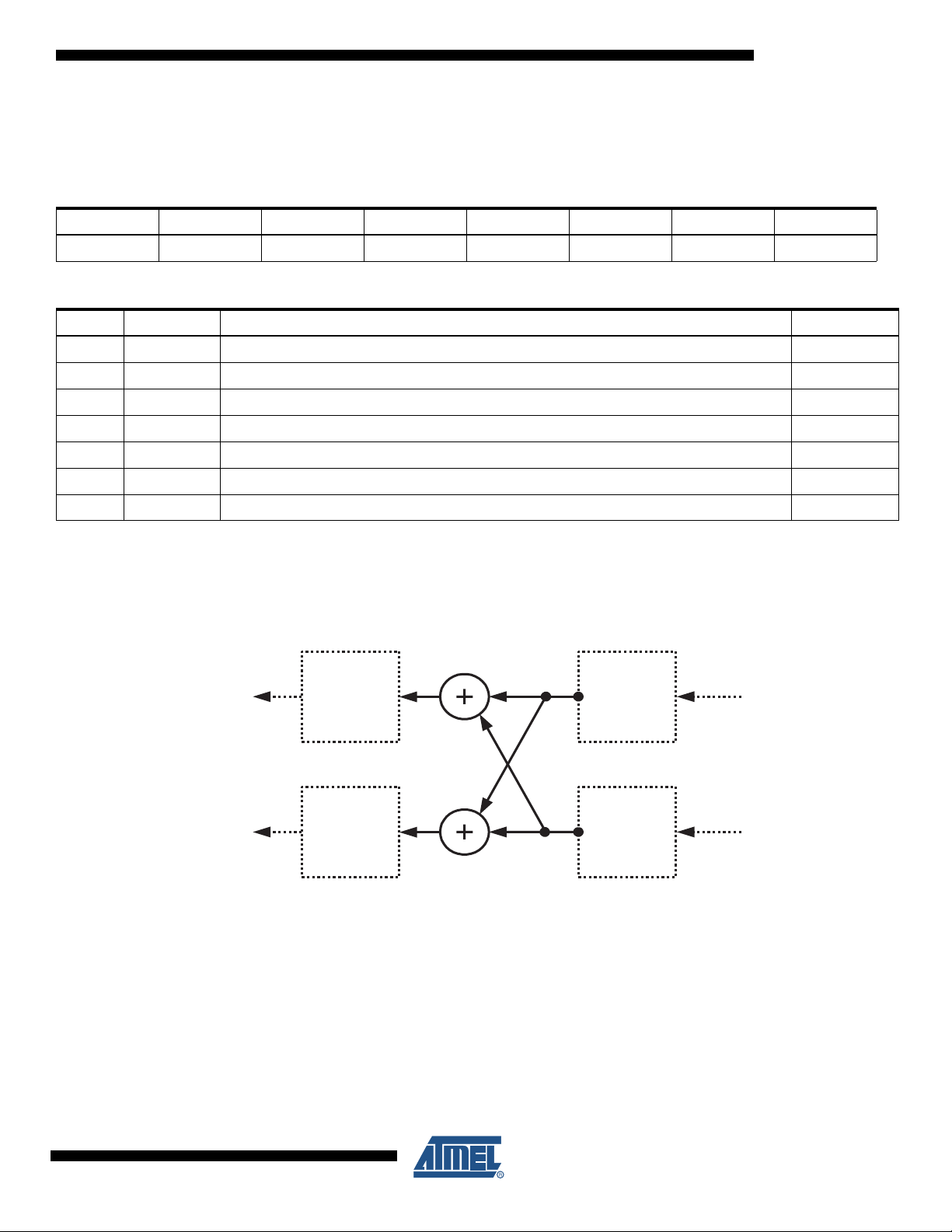
8.5.9 DAC Mixer Control Register Register Name: DAC_MC Access Type: Read/Write Address: 0x08
76543210
RSRV1 RSRV2 INVR INVL RMSMIN2 RSMIN1 LMSMIN2 LMSMIN1
Register (0x08): Mixer Control
Bit Name Description Reset Value
0 LMSMIN1 Left Channel Mono/Stereo Mixer Left Mixed input enable (H to enable, L to disable) LMSMIN1 = 1
1 LMSMIN2 Left Channel Mono/Stereo Mixer Right Mixed input enable (H to enable, L to disable) LMSMIN2 = 0
2 RMSMIN1 Right Channel Mono/Stereo Mixer Left Mixed input enable (H to enable, L to disable) RMSMIN1 = 0
3 RMSMIN2 Right Channel Mono/Stereo Mixer Right Mixed input enable (H to enable, L to disable) RMSMIN2 = 1
4 INVL Left channel mixer output invert (H to enable, L to disable) INVL = 0
5 INVR Right channel mixer output invert (H to enable, L to disable) INVR = 0
7:6 RSRV<1:2> Reserved Bits 00
• Digital Mixer Control
The Audio DAC features a digital mixer that allows the mixing and selection of multiple input sources.
The mixing/multiplexing functions are described in the figure below:
Left channel
Volume
Control
To DACs
Volume
Control
Right channel
Note: Whenever the two mixer inputs are selected, a -6 dB gain is applied to the output signal. Whenever only one input is selected,
no gain is applied.
1
2
1
2
Volume
Control
From digital
filters
Volume
Control
6365A–PMAAC–12-Mar-08
19
 Loading...