

ATMEL ATA5570, AT25DF081 Datasheet

Features
• Single 1.65V - 1.95V Supply
• Serial Peripheral Interface (SPI) Compatible
– Supports SPI Modes 0 and 3
• 66 MHz Maximum Clock Frequency
• Flexible, Uniform Erase Architecture
– 4-Kbyte Blocks
– 32-Kbyte Blocks
– 64-Kbyte Blocks
– Full Chip Erase
• Individual Sector Protection with Global Protect/Unprotect Feature
– Sixteen 64-Kbyte Physical Sectors
• Hardware Controlled Locking of Protected Sectors
• Flexible Programming
– Byte/Page Program (1 to 256 Bytes)
• Automatic Checking and Reporting of Erase/Program Failures
• JEDEC Standard Manufacturer and Device ID Read Methodology
• Low Power Dissipation
– 7 mA Active Read Current (Typical)
– 8 µA Deep Power-Down Current (Typical)
• Endurance: 100,000 Program/Erase Cycles
• Data Retention: 20 Years
• Complies with Full Industrial Temperature Range
• Industry Standard Green (Pb/Halide-free/RoHS Compliant) Package Options
– 8-lead SOIC (150-mil wide)
– 8-contact Ultra Thin DFN (5 mm x 6 mm x 0.6 mm)
– 11-ball dBGA (WLCSP)
8-megabit
1.65-volt
Minimum
SPI Serial Flash
Memory
AT25DF081
1. Description
The AT25DF081 is a serial interface Flash memory device designed for use in a wide
variety of high-volume consumer based applications in which program code is shadowed from Flash memory into embedded or external RAM for execution. The flexible
erase architecture of the AT25DF081, with its erase granularity as small as 4-Kbytes,
makes it ideal for data storage as well, eliminating the need for additional data storage
EEPROM devices.
The physical sectoring and the erase block sizes of the AT25DF081 have been optimized to meet the needs of today's code and data storage applications. By optimizing
the size of the physical sectors and erase blocks, the memory space can be used
much more efficiently. Because certain code modules and data storage segments
must reside by themselves in their own protected sectors, the wasted and unused
memory space that occurs with large sectored and large block erase Flash memory
devices can be greatly reduced. This increased memory space efficiency allows additional code routines and data storage segments to be added while still maintaining the
same overall device density.
3674E–DFLASH–8/08

The AT25DF081 also offers a sophisticated method for protecting individual sectors against
erroneous or malicious program and erase operations. By providing the ability to individually protect and unprotect sectors, a system can unprotect a specific sector to modify its contents while
keeping the remaining sectors of the memory array securely protected. This is useful in applications where program code is patched or updated on a subroutine or module basis, or in
applications where data storage segments need to be modified without running the risk of errant
modifications to the program code segments. In addition to individual sector protection capabilities, the AT25DF081 incorporates Global Protect and Global Unprotect features that allow the
entire memory array to be either protected or unprotected all at once. This reduces overhead
during the manufacturing process since sectors do not have to be unprotected one-by-one prior
to initial programming.
Specifically designed for use in 1.8-volt systems, the AT25DF081 supports read, program, and
erase operations with a supply voltage range of 1.65V to 1.95V. No separate voltage is required
for programming and erasing.
2
AT25DF081
3674E–DFLASH–8/08
2. Pin Descriptions and Pinouts
Table 2-1. Pin Descriptions
Symbol Name and Function
CHIP SELECT: Asserting the CS pin selects the device. When the CS pin is deasserted, the
device will be deselected and normally be placed in standby mode (not Deep Power-Down mode),
and the SO pin will be in a high-impedance state. When the device is deselected, data will not be
CS
SCK
SI
SO
accepted on the SI pin.
A high-to-low transition on the CS
is required to end an operation. When ending an internally self-timed operation such as a program
or erase cycle, the device will not enter the standby mode until the completion of the operation.
SERIAL CLOCK: This pin is used to provide a clock to the device and is used to control the flow of
data to and from the device. Command, address, and input data present on the SI pin is always
latched on the rising edge of SCK, while output data on the SO pin is always clocked out on the
falling edge of SCK.
SERIAL INPUT: The SI pin is used to shift data into the device. The SI pin is used for all data input
including command and address sequences. Data on the SI pin is always latched on the rising
edge of SCK.
SERIAL OUTPUT: The SO pin is used to shift data out from the device. Data on the SO pin is
always clocked out on the falling edge of SCK.
pin is required to start an operation, and a low-to-high transition
AT25DF081
Asserted
State Type
Low Input
Input
Input
Output
WP
HOLD
V
CC
GND
WRITE PROTECT: The WP pin controls the hardware locking feature of the device. Please refer to
“Protection Commands and Features” on page 12 for more details on protection features and the
WP pin.
The WP
not be used. However, it is recommended that the WP pin also be externally connected to VCC
whenever possible.
HOLD: The HOLD pin is used to temporarily pause serial communication without deselecting or
resetting the device. While the HOLD pin is asserted, transitions on the SCK pin and data on the SI
pin will be ignored, and the SO pin will be in a high-impedance state.
The CS
condition to start. A Hold condition pauses serial communication only and does not have an effect
on internally self-timed operations such as a program or erase cycle. Please refer to “Hold” on
page 27 for additional details on the Hold operation.
The HOLD
However, it is recommended that the HOLD pin also be externally connected to VCC whenever
possible.
DEVICE POWER SUPPLY: The VCC pin is used to supply the source voltage to the device.
Operations at invalid V
GROUND: The ground reference for the power supply. GND should be connected to the system
ground.
pin is internally pulled-high and may be left floating if hardware controlled protection will
pin must be asserted, and the SCK pin must be in the low state in order for a Hold
pin is internally pulled-high and may be left floating if the Hold function will not be used.
voltages may produce spurious results and should not be attempted.
CC
Low Input
Low Input
Power
Power
3674E–DFLASH–8/08
3
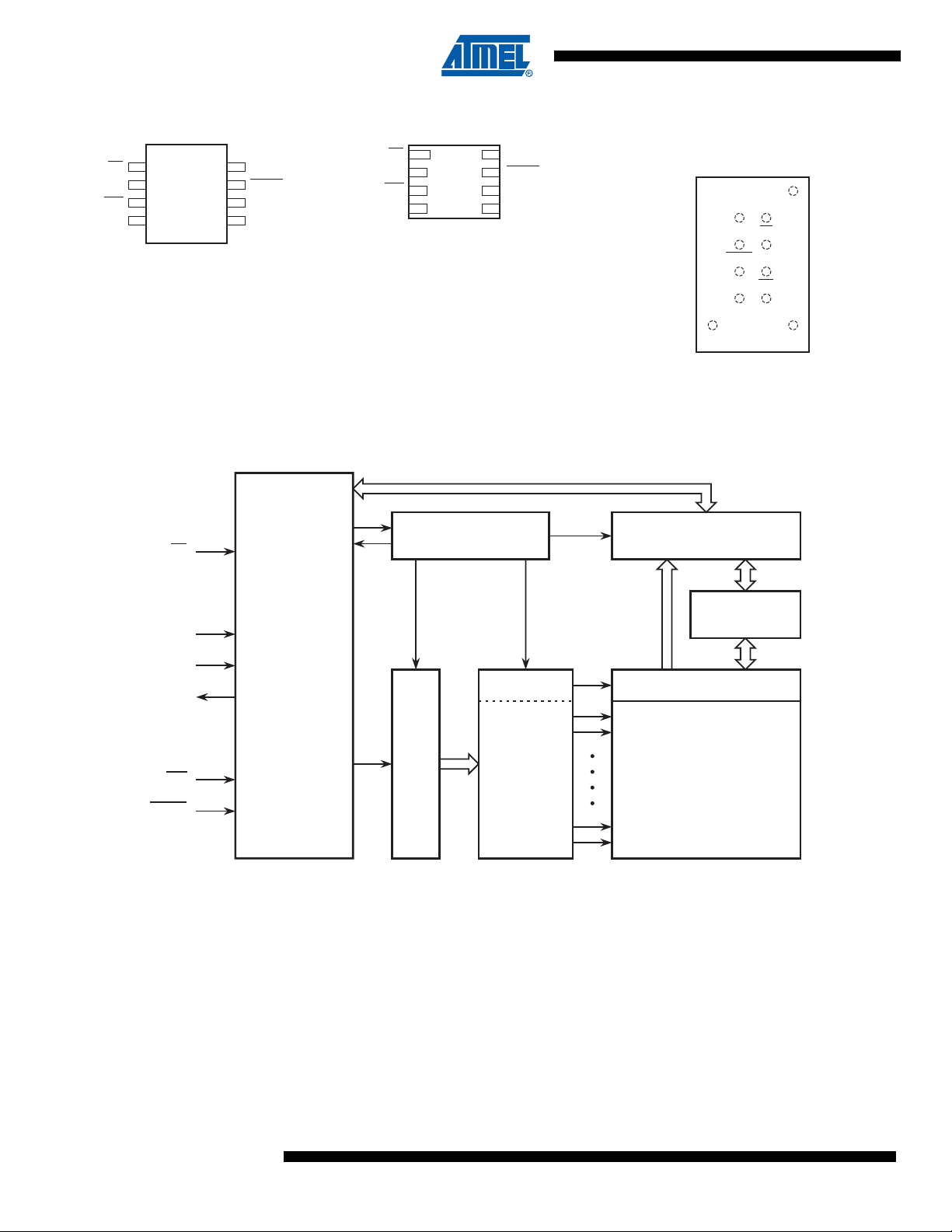
Figure 2-1. 8-SOIC Top View Figure 2-2. 8-UDFN Top View Figure 2-3. 11-dBGA (Top View
1
2
3
4
8
7
6
5
CS
SO
WP
GND
VCC
HOLD
SCK
SI
A
B
C
D
E
F
1
234
NC
VCC
HOLD
SCK
SI
CS
SO
WP
GND
NC
NC
FLASH
MEMORY
ARRAY
Y-GATING
CS
SCK
SO
SI
Y-DECODER
ADDRESS LATCH
X-DECODER
I/O BUFFERS
AND LATCHES
CONTROL AND
PROTECTION LOGIC
SRAM
DATA BUFFER
WP
INTERFACE
CONTROL
AND
LOGIC
HOLD
CS
SO
WP
GND
1
2
3
4
8
7
6
5
VCC
HOLD
SCK
SI
Through Back of Die)
3. Block Diagram
4. Memory Array
4
AT25DF081
To provide the greatest flexibility, the memory array of the AT25DF081 can be erased in four levels of granularity including a full chip erase. In addition, the array has been divided into physical
sectors of uniform size, of which each sector can be individually protected from program and
erase operations. The size of the physical sectors is optimized for both code and data storage
applications, allowing both code and data segments to reside in their own isolated
regions. Figure 4-1 on page 5 illustrates the breakdown of each erase level as well as the breakdown of each physical sector.
3674E–DFLASH–8/08
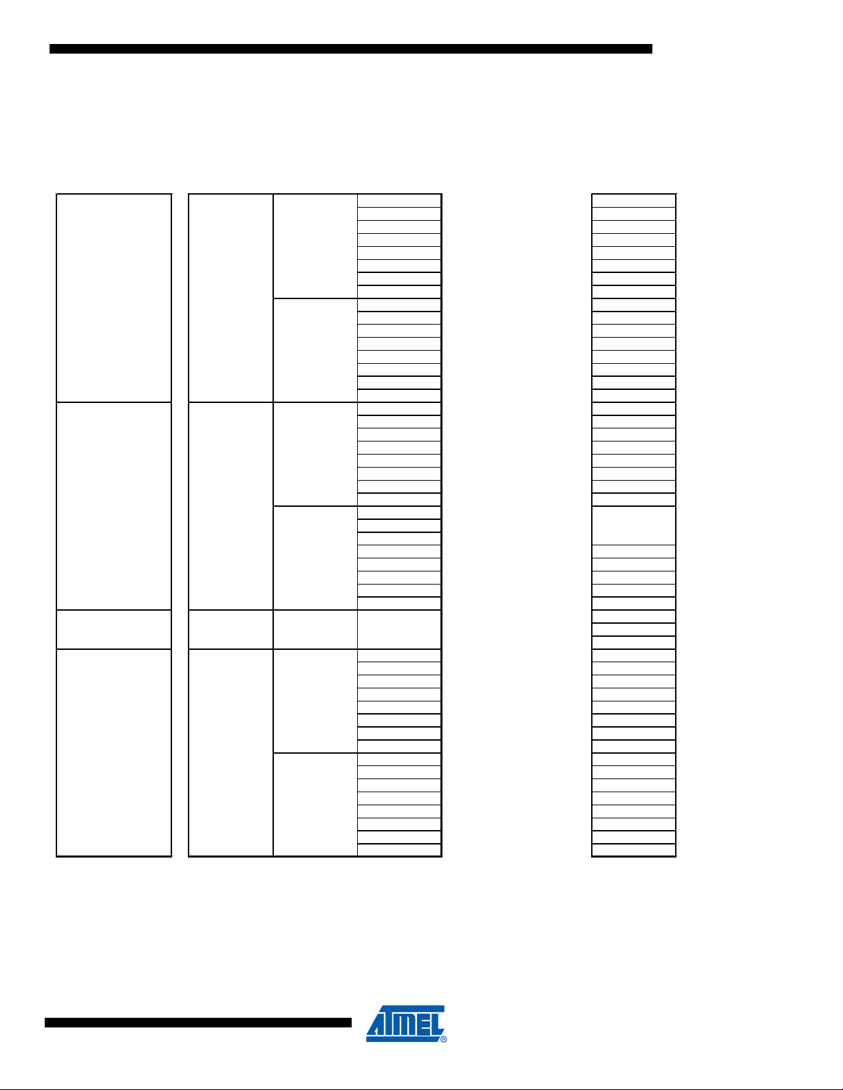
Figure 4-1. Memory Architecture Diagram
64KB
• • •
64KB
32KB
32KB
• • •
• • •
• • •
64KB
64KB
(Sector 15)
32KB
32KB
64KB
(Sector 0)
32KB
32KB
• • •
64KB
(Sector 14)
Block Erase Detail
AT25DF081
Page Program Detail
Internal Sectoring for 64KB 32KB 4KB 1-256 Byte
Sector Protection Block Erase Block Erase Block Erase Page Program
Function (D8h Command) (52h Command) (20h Command) (02h Command)
4KB
4KB
4KB
4KB
4KB
4KB
4KB
4KB
4KB
4KB
4KB
4KB
4KB
4KB
4KB
4KB
4KB
4KB
4KB
4KB
4KB
4KB
4KB
4KB
4KB
4KB
4KB
4KB
4KB
4KB
4KB
4KB
4KB
4KB
4KB
4KB
4KB
4KB
4KB
4KB
4KB
4KB
4KB
4KB
4KB
4KB
4KB
4KB
Range
0FFFFFh– 0FF000h
0FEFFFh– 0FE000h
0FDFFFh – 0FD000h
0FCFFFh– 0FC000h
0FBFFFh– 0FB000h
0FAFFFh– 0FA000h
0F9FFFh – 0F9000h
0F8FFFh – 0F8000h
0F7FFFh – 0F7000h
0F6FFFh – 0F6000h
0F5FFFh – 0F5000h
0F4FFFh – 0F4000h
0F3FFFh – 0F3000h
0F2FFFh – 0F2000h
0F1FFFh – 0F1000h
0F0FFFh – 0F0000h
0EFFFFh–0EF000h
0EEFFFh– 0EE000h
0EDFFFh – 0ED000h
0ECFFFh– 0EC000h
0EBFFFh– 0EB000h
0EAFFFh– 0EA000h
0E9FFFh– 0E9000h
0E8FFFh– 0E8000h
0E7FFFh– 0E7000h
0E6FFFh– 0E6000h
0E5FFFh– 0E5000h
0E4FFFh– 0E4000h
0E3FFFh– 0E3000h
0E2FFFh– 0E2000h
0E1FFFh– 0E1000h
0E0FFFh– 0E0000h
00FFFFh – 00F000h
00EFFFh– 00E000h
00DFFFh – 00D000h
00CFFFh – 00C000h
00BFFFh– 00B000h
00AFFFh –00A000h
009FFFh –009000h
008FFFh –008000h
007FFFh –007000h
006FFFh –006000h
005FFFh –005000h
004FFFh –004000h
003FFFh –003000h
002FFFh –002000h
001FFFh –001000h
000FFFh –000000h
256 Bytes
256 Bytes
256 Bytes
256 Bytes
256 Bytes
256 Bytes
256 Bytes
256 Bytes
256 Bytes
256 Bytes
256 Bytes
256 Bytes
256 Bytes
256 Bytes
256 Bytes
256 Bytes
256 Bytes
256 Bytes
256 Bytes
256 Bytes
256 Bytes
256 Bytes
256 Bytes
256 Bytes
256 Bytes
256 Bytes
256 Bytes
256 Bytes
256 Bytes
256 Bytes
256 Bytes
256 Bytes
256 Bytes
256 Bytes
256 Bytes
256 Bytes
256 Bytes
256 Bytes
256 Bytes
256 Bytes
256 Bytes
256 Bytes
256 Bytes
256 Bytes
256 Bytes
256 Bytes
256 Bytes
256 Bytes
Page AddressBlock Address
Range
0FFFFFh– 0FFF00h
0FFEFFh–0FFE00h
0FFDFFh– 0FFD00h
0FFCFFh– 0FFC00h
0FFBFFh– 0FFB00h
0FFAFFh – 0FFA00h
0FF9FFh– 0FF900h
0FF8FFh– 0FF800h
0FF7FFh– 0FF700h
0FF6FFh– 0FF600h
0FF5FFh– 0FF500h
0FF4FFh– 0FF400h
0FF3FFh– 0FF300h
0FF2FFh– 0FF200h
0FF1FFh– 0FF100h
0FF0FFh– 0FF000h
0FEFFFh– 0FEF00h
0FEEFFh– 0FEE00h
0FEDFFh– 0FED00h
0FECFFh– 0FEC00h
0FEBFFh– 0FEB00h
0FEAFFh– 0FEA00h
0FE9FFh– 0FE900h
0FE8FFh– 0FE800h
0017FFh – 001700h
0016FFh – 001600h
0015FFh – 001500h
0014FFh – 001400h
0013FFh – 001300h
0012FFh – 001200h
0011FFh – 001100h
0010FFh – 001000h
000FFFh –000F00h
000EFFh – 000E00h
000DFFh – 000D00h
000CFFh – 000C00h
000BFFh – 000B00h
000AFFh – 000A00h
0009FFh – 000900h
0008FFh – 000800h
0007FFh – 000700h
0006FFh – 000600h
0005FFh – 000500h
0004FFh – 000400h
0003FFh – 000300h
0002FFh – 000200h
0001FFh – 000100h
0000FFh – 000000h
3674E–DFLASH–8/08
5
5. Device Operation
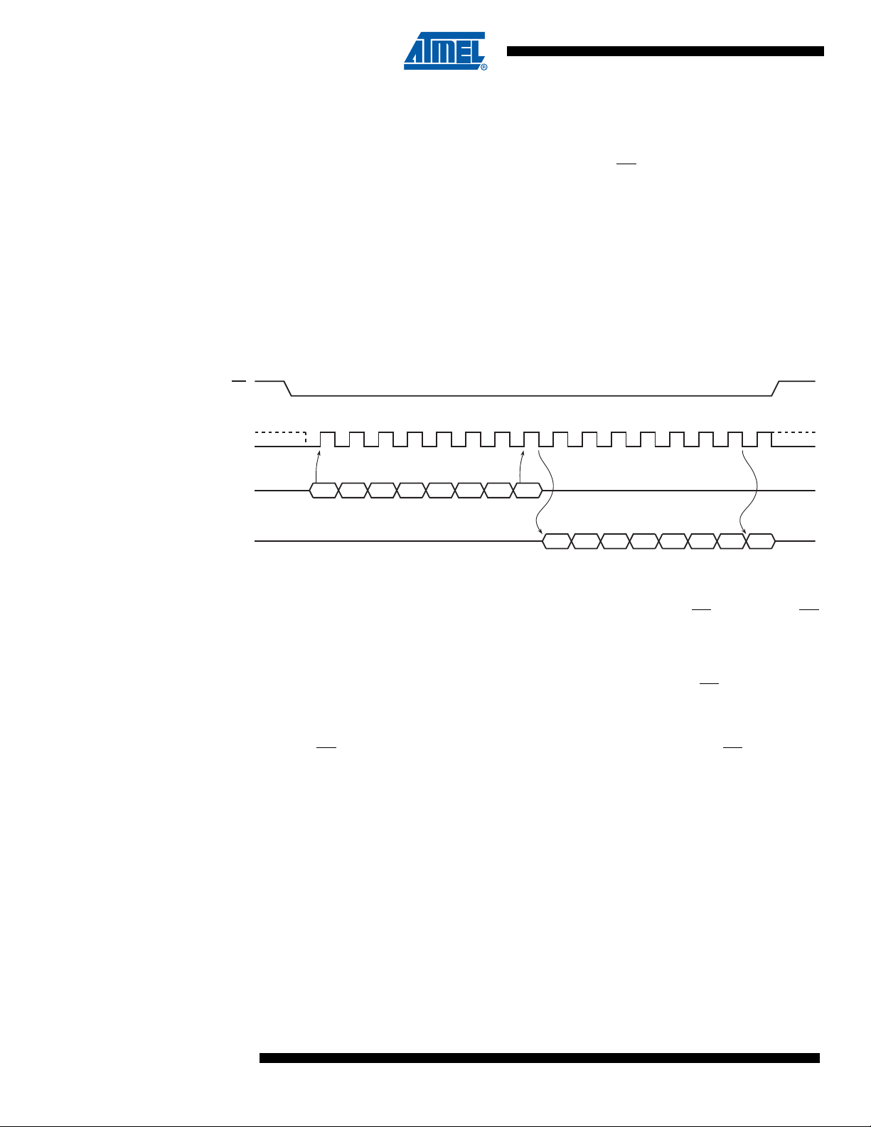
SCK
CS
SI
SO
MSB LSB
MSB
LSB
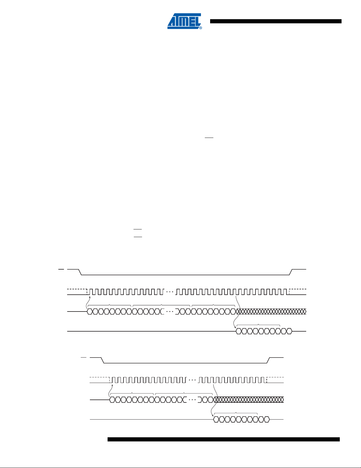
The AT25DF081 is controlled by a set of instructions that are sent from a host controller, commonly referred to as the SPI Master. The SPI Master communicates with the AT25DF081 via the
SPI bus which is comprised of four signal lines: Chip Select (CS
Input (SI), and Serial Output (SO).
The SPI protocol defines a total of four modes of operation (mode 0, 1, 2, or 3) with each mode
differing in respect to the SCK polarity and phase and how the polarity and phase control the
flow of data on the SPI bus. The AT25DF081 supports the two most common modes, SPI
Modes 0 and 3. The only difference between SPI Modes 0 and 3 is the polarity of the SCK signal
when in the inactive state (when the SPI Master is in standby mode and not transferring any
data). With SPI Modes 0 and 3, data is always latched in on the rising edge of SCK and always
output on the falling edge of SCK.
Figure 5-1. SPI Mode 0 and 3
), Serial Clock (SCK), Serial
6. Commands and Addressing
A valid instruction or operation must always be started by first asserting the CS pin. After the CS
pin has been asserted, the SPI Master must then clock out a valid 8-bit opcode on the SPI bus.
Following the opcode, instruction dependent information such as address and data bytes would
then be clocked out by the SPI Master. All opcode, address, and data bytes are transferred with
the most significant bit (MSB) first. An operation is ended by deasserting the CS
Opcodes not supported by the AT25DF081 will be ignored by the device and no operation will be
started. The device will continue to ignore any data presented on the SI pin until the start of the
next operation (CS
serted before complete opcode and address information is sent to the device, then no operation
will be performed and the device will simply return to the idle state and wait for the next
operation.
Addressing of the device requires a total of three bytes of information to be sent, representing
address bits A23-A0. Since the upper address limit of the AT25DF081 memory array is
0FFFFFh, address bits A23-A20 are always ignored by the device.
pin.
pin being deasserted and then reasserted). In addition, if the CS pin is deas-
6
AT25DF081
3674E–DFLASH–8/08
AT25DF081
Table 6-1. Command Listing
Command Opcode Address Bytes Dummy Bytes Data Bytes
Read Commands
Read Array 0Bh 0000 1011 3 1 1+
Read Array (Low Frequency) 03h 0000 0011 3 0 1+
Program and Erase Commands
Block Erase (4-KBytes) 20h 0010 0000 3 0 0
Block Erase (32-KBytes) 52h 0101 0010 3 0 0
Block Erase (64-KBytes) D8h 1101 1000 3 0 0
Chip Erase
Byte/Page Program (1 to 256 Bytes) 02h 0000 0010 3 0 1+
Protection Commands
Write Enable 06h 0000 0110 0 0 0
Write Disable 04h 0000 0100 0 0 0
Protect Sector 36h 0011 0110 3 0 0
Unprotect Sector 39h 0011 1001 3 0 0
60h 0110 0000 0 0 0
C7h 1100 0111 0 0 0
Global Protect/Unprotect Use Write Status Register command
Read Sector Protection Registers 3Ch 0011 1100 3 0 1+
Status Register Commands
Read Status Register 05h 0000 0101 0 0 1+
Write Status Register 01h 0000 0001 0 0 1
Miscellaneous Commands
Read Manufacturer and Device ID 9Fh 1001 1111 0 0 1 to 4
Deep Power-Down B9h 1011 1001 0 0 0
Resume from Deep Power-Down ABh 1010 1011 0 0 0
3674E–DFLASH–8/08
7
7. Read Commands
SCK
CS
SI
SO
MSB MSB
2310
00001011
675410119812 394243414037 3833 36353431 3229 30 44 47 484645
OPCODE
AAAA AAAA A
MSB
XXXXXXXX
MSB MSB
DDDDDDDDDD
ADDRESS BITS A23-A0 DON'T CARE
DATA BYTE 1
HIGH-IMPEDANCE
SCK
CS
SI
SO
MSB MSB
2310
00000011
675410119812 373833 36353431 3229 30 39 40
OPCODE
AAAA AAAA A
MSB MSB
DDDDDDDDDD
ADDRESS BITS A23-A0
DATA BYTE 1
HIGH-IMPEDANCE
7.1 Read Array
The Read Array command can be used to sequentially read a continuous stream of data from
the device by simply providing the SCK signal once the initial starting address has been specified. The device incorporates an internal address counter that automatically increments on every
clock cycle.
Two opcodes, 0Bh and 03h, can be used for the Read Array command. The use of each opcode
depends on the maximum SCK frequency that will be used to read data from the device. The
0Bh opcode can be used at any SCK frequency up to the maximum specified by f
opcode can be used for lower frequency read operations up to the maximum specified by f
To perform the Read Array operation, the CS
opcode (0Bh or 03h) must be clocked into the device. After the opcode has been clocked in, the
three address bytes must be clocked in to specify the starting address location of the first byte to
read within the memory array. If the 0Bh opcode is used, then one don’t care byte must also be
clocked in after the three address bytes.
After the three address bytes (and the one don’t care byte if using opcode 0Bh) have been
clocked in, additional clock cycles will result in serial data being output on the SO pin. The data
is always output with the MSB of a byte first. When the last byte (0FFFFFh) of the memory array
has been read, the device will continue reading back at the beginning of the array (000000h). No
delays will be incurred when wrapping around from the end of the array to the beginning of the
array.
. The 03h
SCK
RDLF
pin must first be asserted and the appropriate
.
Deasserting the CS
ance state. The CS
data be read.
Figure 7-1. Read Array – 0Bh Opcode
Figure 7-2. Read Array – 03h Opcode
pin will terminate the read operation and put the SO pin into a high-imped pin can be deasserted at any time and does not require that a full byte of
8
AT25DF081
3674E–DFLASH–8/08

8. Program and Erase Commands
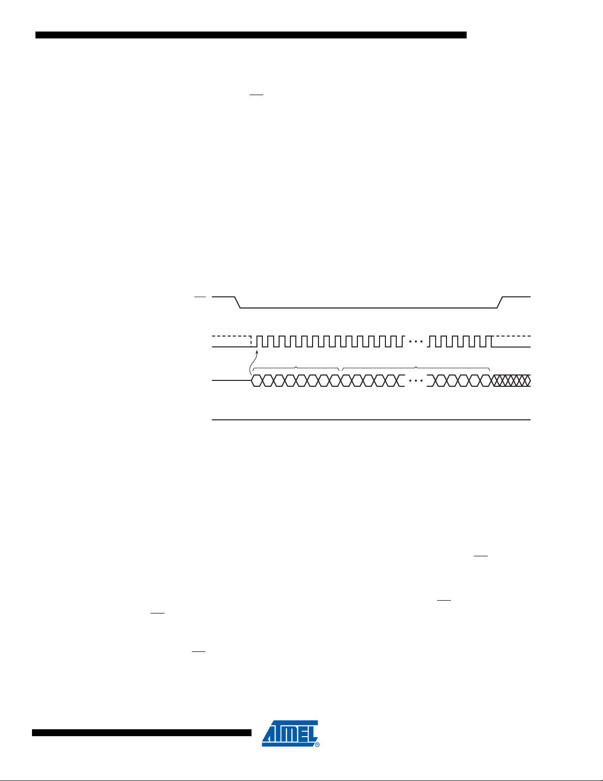
8.1 Byte/Page Program
The Byte/Page Program command allows anywhere from a single byte of data to 256 bytes of
data to be programmed into previously erased memory locations. An erased memory location is
one that has all eight bits set to the logical “1” state (a byte value of FFh). Before a Byte/Page
Program command can be started, the Write Enable command must have been previously
issued to the device (see Write Enable command description) to set the Write Enable Latch
(WEL) bit of the Status Register to a logical “1” state.
To perform a Byte/Page Program command, an opcode of 02h must be clocked into the device
followed by the three address bytes denoting the first byte location of the memory array to begin
programming at. After the address bytes have been clocked in, data can then be clocked into the
device and will be stored in an internal buffer.
If the starting memory address denoted by A23-A0 does not fall on an even 256-byte page
boundary (A7-A0 are not all 0), then special circumstances regarding which memory locations
will be programmed will apply. In this situation, any data that is sent to the device that goes
beyond the end of the page will wrap around back to the beginning of the same page. For example, if the starting address denoted by A23-A0 is 0000FEh, and three bytes of data are sent to
the device, then the first two bytes of data will be programmed at addresses 0000FEh and
0000FFh while the last byte of data will be programmed at address 000000h. The remaining
bytes in the page (addresses 000001h through 0000FDh) will be unaffected and will not change.
In addition, if more than 256 bytes of data are sent to the device, then only the last 256 bytes
sent will be latched into the internal buffer.
AT25DF081
When the CS
gram it into the appropriate memory array locations based on the starting address specified by
A23-A0 and the number of complete data bytes sent to the device. If less than 256 bytes of data
were sent to the device, then the remaining bytes within the page will not be altered. The programming of the data bytes is internally self-timed and should take place in a time of t
The three address bytes and at least one complete byte of data must be clocked into the device
before the CS
(multiples of eight bits); otherwise, the device will abort the operation and no data will be programmed into the memory array. In addition, if the address specified by A23-A0 points to a
memory location within a sector that is in the protected state (see “Protect Sector” on page 13),
then the Byte/Page Program command will not be executed, and the device will return to the idle
state once the CS
back to the logical “0” state if the program cycle aborts due to an incomplete address being sent,
an incomplete byte of data being sent, or because the memory location to be programmed is
protected.
While the device is programming, the Status Register can be read and will indicate that the
device is busy. For faster throughput, it is recommended that the Status Register be polled
rather than waiting the t
some point before the program cycle completes, the WEL bit in the Status Register will be reset
back to the logical “0” state.
The device also incorporates an intelligent programming algorithm that can detect when a byte
location fails to program properly. If a programming error arises, it will be indicated by the EPE
bit in the Status Register.
pin is deasserted, the device will take the data stored in the internal buffer and pro-
.
PP
pin is deasserted, and the CS pin must be deasserted on even byte boundaries
pin has been deasserted. The WEL bit in the Status Register will be reset
time to determine if the data bytes have finished programming. At
PP
3674E–DFLASH–8/08
9
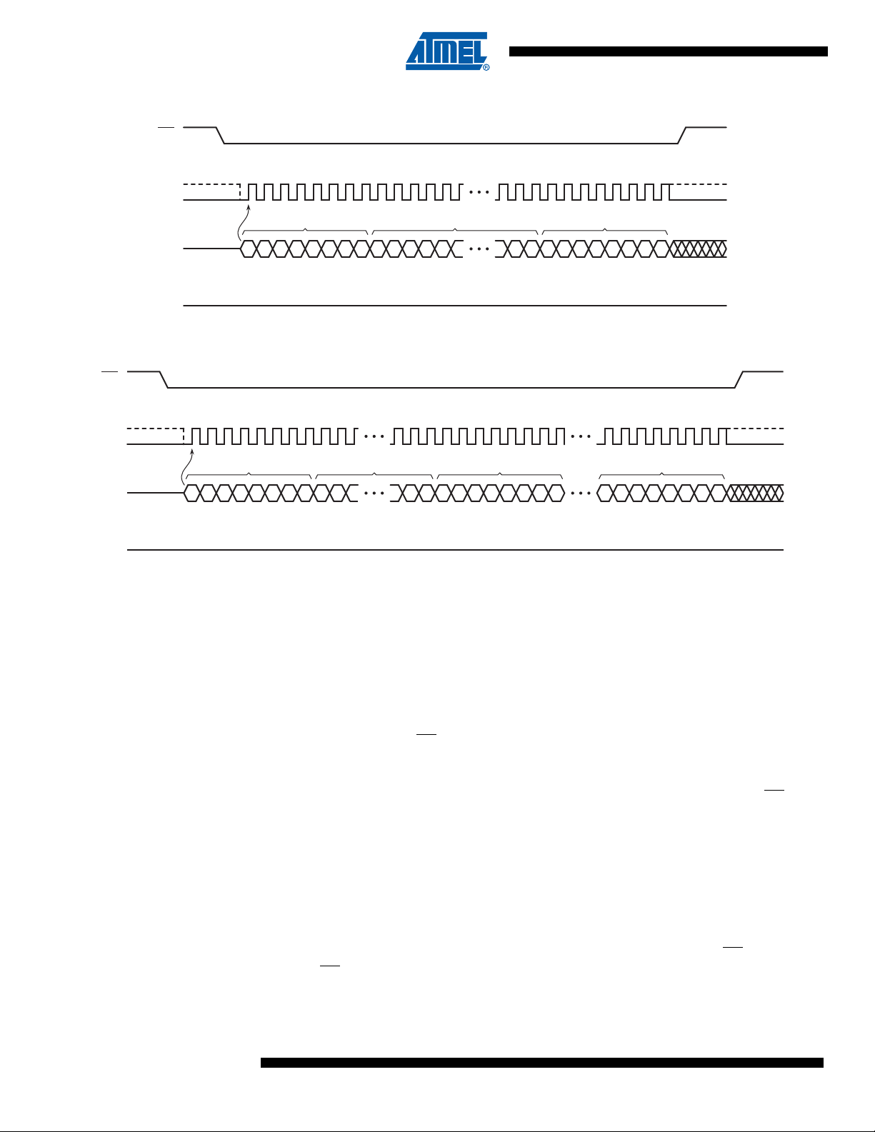
Figure 8-1. Byte Program
SCK
CS
SI
SO
MSB MSB
2310
00000010
6754983937 3833 36353431 3229 30
OPCODE
HIGH-IMPEDANCE
AA AAAA
MSB
DDDDDDDD
ADDRESS BITS A23-A0 DATA IN BYTE 1
MSB
DDDDDDDD
DATA IN BYTE n
CS
SCK
SI
SO
Figure 8-2. Page Program
2310
OPCODE
00000010
MSB MSB
HIGH-IMPEDANCE
675410119812 3937 3833 36353431 3229 30
ADDRESS BITS A23-A0 DATA IN
AAAA AAAA A
DDDDDDDD
MSB
8.2 Block Erase
A block of 4K-, 32K-, or 64K-bytes can be erased (all bits set to the logical “1” state) in a single
operation by using one of three different opcodes for the Block Erase command. An opcode of
20h is used for a 4K-byte erase, an opcode of 52h is used for a 32K-byte erase, and an opcode
of D8h is used for a 64K-byte erase. Before a Block Erase command can be started, the Write
Enable command must have been previously issued to the device to set the WEL bit of the Status Register to a logical “1” state.
To perform a Block Erase, the CS
pin must first be asserted and the appropriate opcode (20h,
52h, or D8h) must be clocked into the device. After the opcode has been clocked in, the three
address bytes specifying an address within the 4K-, 32K-, or 64K-byte block to be erased must
be clocked in. Any additional data clocked into the device will be ignored. When the CS
deasserted, the device will erase the appropriate block. The erasing of the block is internally
self-timed and should take place in a time of t
BLKE
.
Since the Block Erase command erases a region of bytes, the lower order address bits do not
need to be decoded by the device. Therefore, for a 4K-byte erase, address bits A11-A0 will be
ignored by the device and their values can be either a logical “1” or “0”. For a 32K-byte erase,
address bits A14-A0 will be ignored, and for a 64K-byte erase, address bits A15-A0 will be
ignored by the device. Despite the lower order address bits not being decoded by the device, the
complete three address bytes must still be clocked into the device before the CS
serted, and the CS
otherwise, the device will abort the operation and no erase operation will be performed.
pin must be deasserted on an even byte boundary (multiples of eight bits);
pin is deas-
pin is
10
AT25DF081
3674E–DFLASH–8/08
AT25DF081
If the address specified by A23-A0 points to a memory location within a sector that is in the protected state, then the Block Erase command will not be executed, and the device will return to
the idle state once the CS
The WEL bit in the Status Register will be reset back to the logical “0” state if the erase cycle
aborts due to an incomplete address being sent or because a memory location within the region
to be erased is protected.
While the device is executing a successful erase cycle, the Status Register can be read and will
indicate that the device is busy. For faster throughput, it is recommended that the Status Register be polled rather than waiting the t
some point before the erase cycle completes, the WEL bit in the Status Register will be reset
back to the logical “0” state.
The device also incorporates an intelligent erasing algorithm that can detect when a byte location fails to erase properly. If an erase error arises, it will be indicated by the EPE bit in the
Status Register.
Figure 8-3. Block Erase
CS
pin has been deasserted.
time to determine if the device has finished erasing. At
BLKE
8.3 Chip Erase
2310
675410119812 3129 3027 2826
SCK
SI
SO
OPCODE
CCCCCCCC
MSB MSB
HIGH-IMPEDANCE
AAAA AAAA A A A A
ADDRESS BITS A23-A0
The entire memory array can be erased in a single operation by using the Chip Erase command.
Before a Chip Erase command can be started, the Write Enable command must have been previously issued to the device to set the WEL bit of the Status Register to a logical “1” state.
Two opcodes, 60h and C7h, can be used for the Chip Erase command. There is no difference in
device functionality when utilizing the two opcodes, so they can be used interchangeably. To
perform a Chip Erase, one of the two opcodes (60h or C7h) must be clocked into the device.
Since the entire memory array is to be erased, no address bytes need to be clocked into the
device, and any data clocked in after the opcode will be ignored. When the CS
pin is deasserted,
the device will erase the entire memory array. The erasing of the device is internally self-timed
and should take place in a time of t
The complete opcode must be clocked into the device before the CS
CS
pin must be deasserted on an even byte boundary (multiples of eight bits); otherwise, no
CHPE
.
pin is deasserted, and the
erase will be performed. In addition, if any sector of the memory array is in the protected state,
then the Chip Erase command will not be executed, and the device will return to the idle state
once the CS
pin has been deasserted. The WEL bit in the Status Register will be reset back to
the logical “0” state if a sector is in the protected state.
3674E–DFLASH–8/08
While the device is executing a successful erase cycle, the Status Register can be read and will
indicate that the device is busy. For faster throughput, it is recommended that the Status Regis-
11
ter be polled rather than waiting the t
SCK
CS
SI
SO
MSB
2310
00000110
6754
OPCODE
HIGH-IMPEDANCE
time to determine if the device has finished erasing. At
CHPE
some point before the erase cycle completes, the WEL bit in the Status Register will be reset
back to the logical “0” state.
The device also incorporates an intelligent erasing algorithm that can detect when a byte location fails to erase properly. If an erase error arises, it will be indicated by the EPE bit in the
Status Register.
Figure 8-4. Chip Erase
CS
SCK
SI
SO
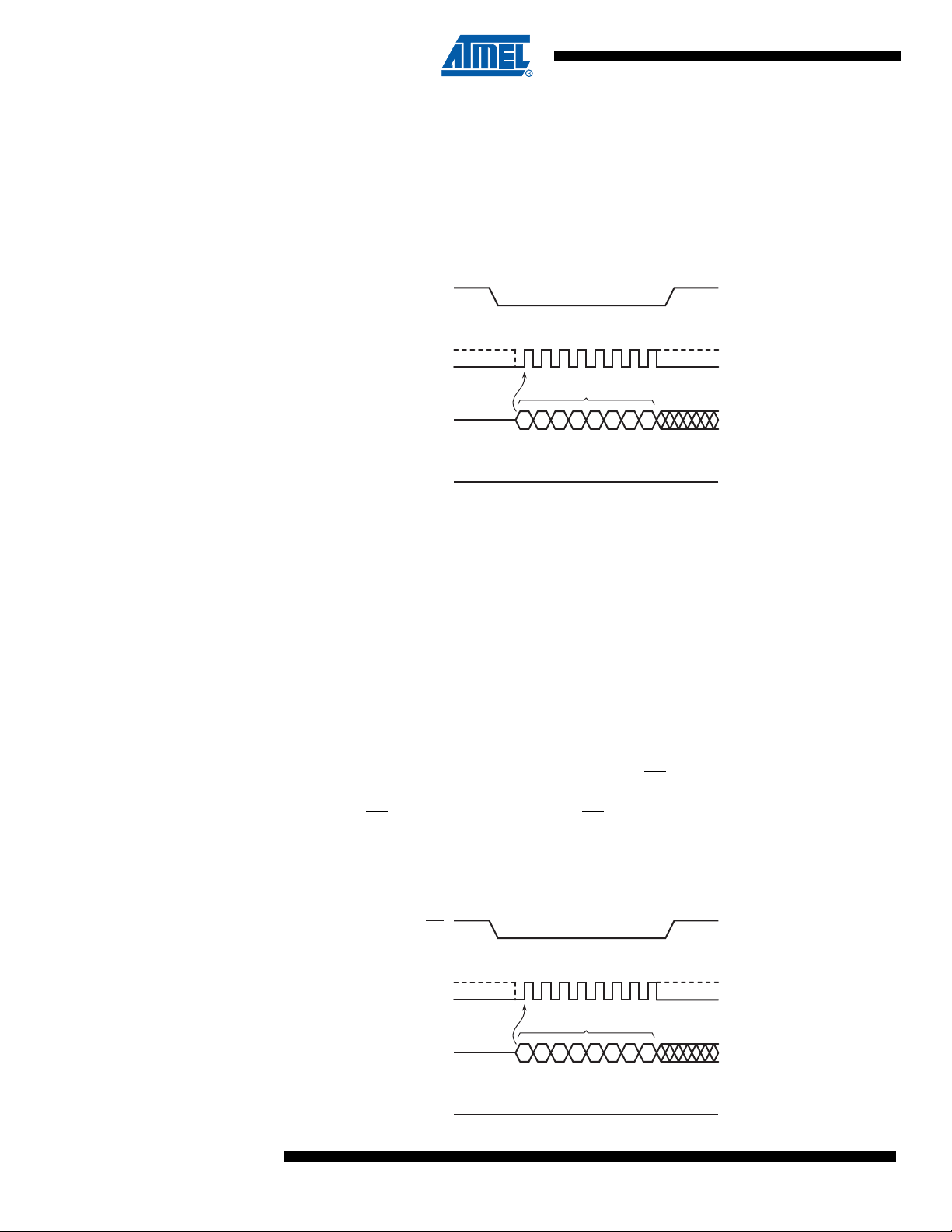
9. Protection Commands and Features
9.1 Write Enable
The Write Enable command is used to set the Write Enable Latch (WEL) bit in the Status Register to a logical “1” state. The WEL bit must be set before a program, erase, Protect Sector,
Unprotect Sector, or Write Status Register command can be executed. This makes the issuance
of these commands a two step process, thereby reducing the chances of a command being
accidentally or erroneously executed. If the WEL bit in the Status Register is not set prior to the
issuance of one of these commands, then the command will not be executed.
To issue the Write Enable command, the CS
must be clocked into the device. No address bytes need to be clocked into the device, and any
data clocked in after the opcode will be ignored. When the CS
the Status Register will be set to a logical “1”. The complete opcode must be clocked into the
device before the CS
boundary (multiples of eight bits); otherwise, the device will abort the operation and the state of
the WEL bit will not change.
pin is deasserted, and the CS pin must be deasserted on an even byte
2310
OPCODE
CCCCCCCC
MSB
HIGH-IMPEDANCE
6754
pin must first be asserted and the opcode of 06h
pin is deasserted, the WEL bit in
12
AT25DF081
Figure 9-1. Write Enable
3674E–DFLASH–8/08
 Loading...