ATMEL ATA5567, AT42QT2160 Datasheet

Features
• Number of keys: up to 16 keys, and one slider (constructed from 2 to 8 keys)
• Number of I/O lines: 11 (3 dedicated - configurable for input or output, 8 shared -
output only), PWM control for LED driving
• Technology: patented spread-spectrum charge-transfer (transverse mode)
• Key outline sizes: 6 mm x 6 mm or larger (panel thickness dependent); widely different
sizes and shapes possible
• Key spacings: 8 mm or wider, center to center (panel thickness dependent)
• Slider design: 2 to 8 keys placed in sequence, same design as keys
• Electrode design: two-part electrode shapes (drive-receive); wide variety of possible
layouts
• PCB layers required: one layer (with jumpers), two layers (no jumpers)
• Electrode materials: PCB, FPCB, silver or carbon on film, ITO on film
• Panel materials: plastic, glass, composites, painted surfaces (low particle density
metallic paints possible)
• Adjacent metal: compatible with grounded metal immediately next to keys
• Panel thickness: up to 3 mm glass, 2.5 mm plastic (key size dependent)
• Key sensitivity: individually settable via simple commands over I
2
C-compatible
interface
• Interface: I
2
C-compatible slave mode (100kHz)
• Moisture tolerance: best in class
• Power: 1.8 V to 5.5 V
• Package: 28-pin 4 x 4 mm MLF RoHS compliant
• Signal processing: self-calibration, auto drift compensation, noise filtering, Adjacent
Key Suppression
TM
technology
• Applications: laptop, mobile, consumer appliances, PC peripheral etc.
• Patents: AKS™ (patented Adjacent Key Suppression™) technology
QMatrix™ (patented charge-transfer method)
QSlide™ (patented charge-transfer method) (patent-pending QSlide sensing
configuration)
• This datasheet is applicable to revision 4R0 chips only
1. Overview
The AT42QT2160-MMU (QT2160) is designed for use with up to 16 keys and a slider
(constructed from 2 keys up to 8 keys). There are three dedicated General Purpose
Input/Outputs (GPIOs) which can be used as inputs for mechanical switches etc. or as driven
outputs. There are eight shared General Purpose Outputs (GPOs) (X0...X7) which are driven
outputs only. There is PWM control for all GPIO/GPOs.
The QMatrix™ technology employs transverse charge-transfer sensing electrode
designs which can be made very compact and are easily wired. Charge is forced from
an emitting electrode into the overlying panel dielectric, and then collected on a
receiver electrode. This directs the charge into a sampling capacitor which is then
converted directly to digital form, without the use of amplifiers.
The keys are configured in a matrix format that minimizes the number of required scan
lines and device pins. The key electrodes can be designed into a conventional Printed
Circuit Board (PCB) or Flexible Printed Circuit Board (FPCB) as a copper pattern, or
as printed conductive ink on plastic film.
9502A–AT42–07/08
QSlide™, 16-key
QMatrix™
Sensor IC
AT42QT2160
2
9502A–AT42–07/08
AT42QT2160
2. Pinout and Pin Listing Description
2.1 Pinout Description
2.2 Pin Listing Description
GPIO1
Y1A
Y0A
RST
VRef
X0
X2
GPIO2
GPIO3
VSS
VDD
X6
VSS
Y0B
Y1B
1
2
3
4
5
6
715
16
17
18
19
20
21
28
27
26
25
24 23
22
89 1413
12
11
10
QT2160
X7
CHANGE
X3
X4
VDD
I2CA0
SMP
X1
X5
VDD
I2CA1
SDA
SCL
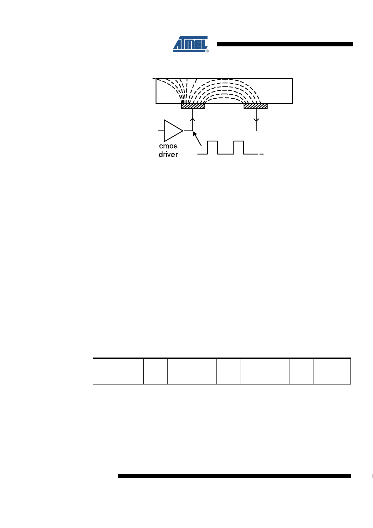
Table 2-1.Pin Listing
Pin Function I/O Comments
If Unused,
Connect To...
1 GPIO2 I/O General purpose input/output 2 -
2 GPIO3 I/O General purpose input/output 3 -
3 Vdd P Power -
4 Vss P Supply ground -
5 X6 O X matrix drive line / shared GPO X6 Leave open
6 X7 O X matrix drive line / shared GPO X7 Leave open
7 CHANGE
OD State change notification Leave open
8 Vref P Supply ground -
9 SMP O Sample output. -
10 X0 O X matrix drive line / shared GPO X0 Leave open
11 X1 O X matrix drive line / shared GPO X1 Leave open
12 X2 O X matrix drive line / shared GPO X2 Leave open
13 X3 O X matrix drive line / shared GPO X3 Leave open

3
9502A–AT42–07/08
AT42QT2160
3. Introduction
The QT2160 device is a digital burst mode charge-transfer (QT) sensor designed specifically for
matrix layout touch controls; it includes all signal processing functions necessary to provide
stable sensing under a wide variety of changing conditions. Only a few external parts are
required for operation. The entire circuit can be built within a few square centimeters of
single-sided PCB area. CEM-1 and FR1 punched, single-sided materials can be used for the
lowest possible cost. The PCB’s rear can be mounted flush on the back of a glass or plastic
panel using a conventional adhesive, such as 3M VHB two-sided adhesive acrylic film.
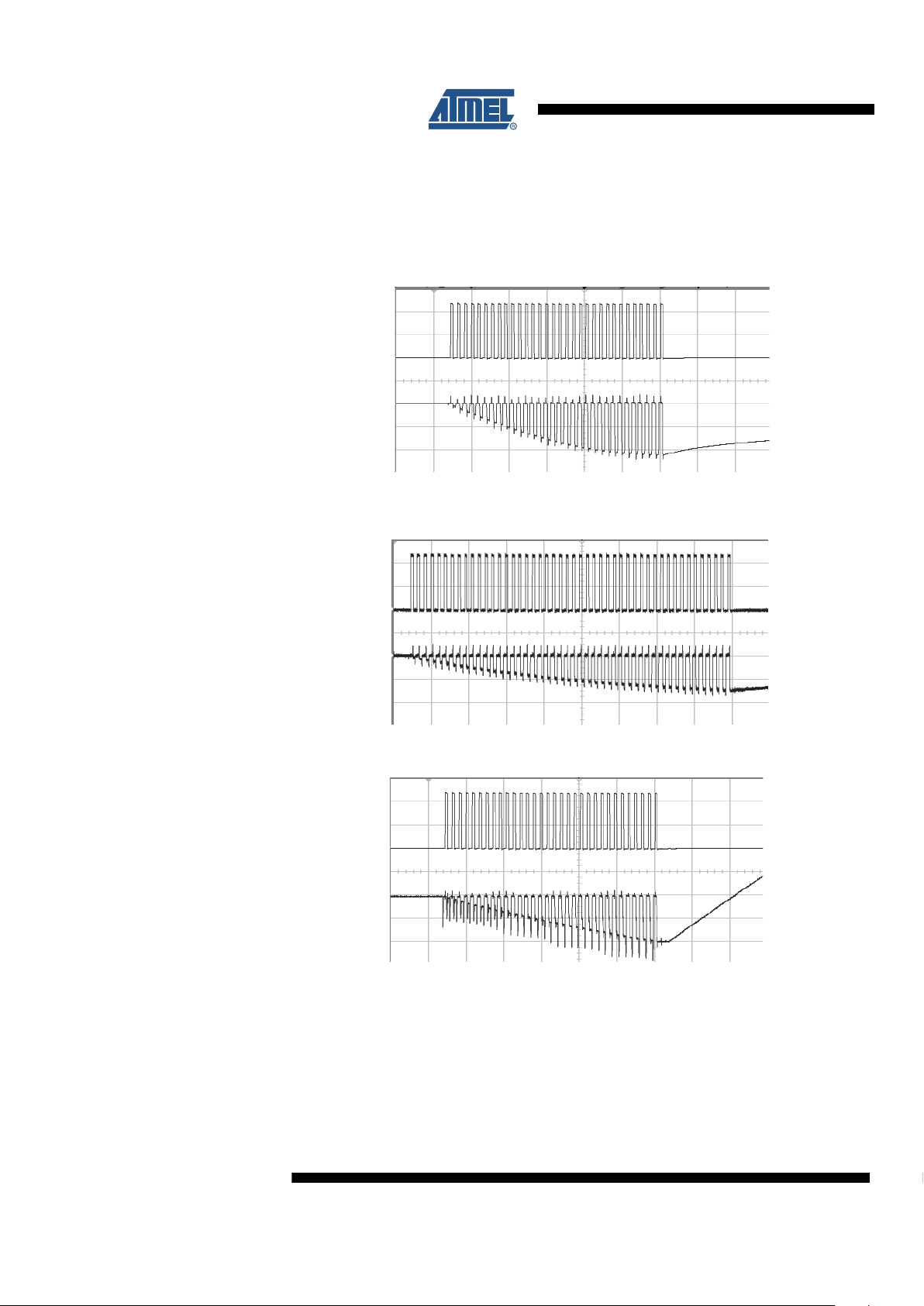
The QT2160 employs transverse charge-transfer (QT) sensing, a technology that senses
changes in electrical charge forced across two electrode elements by a pulse edge (see
Figure 3-1). The QT2160 allows a wide range of key sizes and shapes to be mixed together in a
single touch panel.
The device uses an
I2C-compatible interface to allow key data to be extracted and to permit
individual key parameter setup. The command structure is designed to minimize the amount of
data traffic while maximizing the amount of information conveyed.
In addition to normal operating and setup functions the device can also report back actual signal
strengths.
14 X4 O X matrix drive line / shared GPO X4 Leave open
15 X5 O X matrix drive line / shared GPO X5 Leave open
16 Vdd P Power -
17 Vdd P Power -
18 Vss P Supply ground -
19 Y0B I/O Y line connection Leave open
20 Y1B I/O Y line connection Leave open
21 I2CA0 I I
2
C-compatible address select -
22 I2CA1 I I
2
C-compatible address select -
23 SDA OD Serial Interface Data -
24 SCL OD Serial Interface Clock -
25 RST
I
Reset low; has internal 30k - 60k pull-upLeave open or
Vdd
26 Y0A I/O Y line connection Leave open
27 Y1A I/O Y line connection Leave open
28 GPIO1 I/O General purpose input/output 1
Table 2-1.Pin Listing (continued)
Pin Function I/O Comments
If Unused,
Connect To...
4
9502A–AT42–07/08
AT42QT2160
Figure 3-1. Field Flow Between X and Y Elements
3.1 Keys and Slider
The QT2160 is capable of a maximum of 16 keys. These can be located anywhere within an
electrical grid of 8X and 2Y scan lines.
A lesser number of enabled keys will cause any unused acquisition burst timeslots to be pared
from the sampling sequence, to optimize acquire speed and lessen power consumption. Thus, if
only 8 keys are actually enabled, only 8 timeslots are used for scanning.
Additional processing can be done on the keys to form a slider. The slider will have to start at X0
and use only Y0. The slider can consist of a minimum of 2 keys and a maximum of 8 keys.
3.2 Enabling/Disabling Keys
Keys can be enabled by setting a nonzero burst length. A zero burst length disables the key.
4. Hardware and Functional
4.1 Matrix Scan Sequence
The circuit operates by scanning each key sequentially, key by key. Key scanning begins with
location X = 0, Y = 0 (key 0). X axis keys are known as rows while Y axis keys are referred to as
columns although this has no reflection on actual wiring. Keys are scanned sequentially by row,
for example the sequence X0Y0 X1Y0...X7Y0, X0Y1, X1Y1... etc. Keys are also numbered from
0...15. Key 0 is located at X0Y0. Table 4-1 shows the key numbering.
Table 4-1. Key Numbers
Each key is sampled in a burst of acquisition pulses whose length is determined by the Setups
parameter BL (Section 4.2 on page 5); this can be set on a per-key basis. A burst is completed
entirely before the next key is sampled; at the end of each burst the resulting signal is converted
to digital form and processed. The burst length directly impacts key gain; each key can have a
unique burst length in order to allow tailoring of key sensitivity on a key-by-key basis.
overlying panel
X
element
Y
element
X7 X6 X5 X4 X3 X2 X1 X0
Y0 76543210
Key numbers
Y1 15 14 13 12 11 10 9 8

5
9502A–AT42–07/08
AT42QT2160
4.2 Burst Paring
Keys that are disabled by setting their burst length to zero have their bursts removed from the
scan sequence to save scan time and thus power. The QT2160 operates on a fixed 16 ms cycle
and will go to sleep after all acquisitions and processing is done till the next 16ms cycle starts.
As a consequence, the fewer keys, the less power is consumed.
4.3 Cs Sample Capacitor Operation
Cs capacitors (Cs0...Cs1) absorb charge from the key electrodes on the rising edge of each X
pulse. On each falling edge of X, the Y matrix line is clamped to ground to allow the electrode
and wiring charges to neutralize in preparation for the next pulse. With each X pulse charge
accumulates on Cs causing a staircase increase in its differential voltage.
After the burst completes, the device clamps the Y line to ground causing the opposite terminal
to go negative. The charge on Cs is then measured using an external resistor to ramp the
negative terminal upwards until a zero crossing is achieved. The time required to zero cross
becomes the measurement result.
The Cs capacitors should be connected as shown in Figure 4-8 on page 15. The value of these
capacitors is not critical but 4.7 nF is recommended for most cases. They should be 10 percent
X7R ceramic. If the transverse capacitive coupling from X to Y is large enough the voltage on a
Cs capacitor can saturate, destroying gain. In such cases the burst length should be reduced
and/or the Cs value increased. See Section 4.4.
If a Y line is not used its corresponding Cs capacitor may be omitted and the pins left floating.
4.4 Sample Capacitor Saturation
Cs voltage saturation at a pin YnB is shown in Figure 4-1. Saturation begins to occur when the
voltage at a YnB pin becomes more negative than -0.25V at the end of the burst. This
nonlinearity is caused by excessive voltage accumulation on Cs inducing conduction in the pin
protection diodes. This badly saturated signal destroys key gain and introduces a strong thermal
coefficient which can cause phantom detection. The cause of this is either from the burst length
being too long, the Cs value being too small, or the X-Y transfer coupling being too large.
Solutions include loosening up the key structure interleaving, more separation of the X and Y
lines on the PCB, increasing Cs, and decreasing the burst length.
Increasing Cs will make the part slower; decreasing burst length will make it less sensitive. A
better PCB layout and a looser key structure (up to a point) have no negative effects.
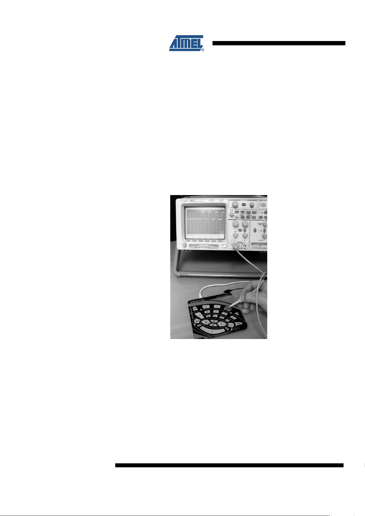
Cs voltages should be observed on an oscilloscope with the matrix layer bonded to the panel
material; if the Rs side of any Cs ramps more negative than -0.25 volts during any burst (not
counting overshoot spikes which are probe artifacts), there is a potential saturation problem.
Figure 4-2 shows a defective waveform similar to that of Figure 4-1, but in this case the
distortion is caused by excessive stray capacitance coupling from the Y line to AC ground; for
example, from running too near and too far alongside a ground trace, ground plane, or other
traces. The excess coupling causes the charge-transfer effect to dissipate a significant portion of
the received charge from a key into the stray capacitance. This phenomenon is more subtle; it
can be best detected by increasing BL to a high count and watching what the waveform does as
it descends towards and below -0.25V. The waveform will appear deceptively straight, but it will
slowly start to flatten even before the -0.25V level is reached.
A correct waveform is shown in Figure 4-3. Note that the bottom edge of the bottom trace is
substantially straight (ignoring the downward spikes).
6
9502A–AT42–07/08
AT42QT2160
Unlike other QT circuits, the Cs capacitor values on QT2160 devices have no effect on
conversion gain. However, they do affect conversion time.
Unused Y lines should be left open.
Figure 4-1. VCs – Nonlinear During Burst
(Burst too long, or Cs too small, or X-Y transcapacitance too large)
Figure 4-2. VCs – Poor Gain, Nonlinear During Burst
(Excess capacitance from Y line to Gnd)
Figure 4-3. VCs – Correct
X Driv
eYnB
X Driv
eYnB
X Driv
e
Yn
B

7
9502A–AT42–07/08
AT42QT2160
Figure 4-4. Drive Pulse Roll-off and Dwell Time
Note: The Dwell time is a minimum of ~250ns - see Section 4.7
4.5 Sample Resistors
The sample resistors (Rs0...Rs1) are used to perform single-slope ADC conversion of the
acquired charge on each Cs capacitor. These resistors directly control acquisition gain; larger
values of Rs will proportionately increase signal gain. For most applications Rs should be 1MΩ.
Unused Y lines do not require an Rs resistor.
4.6 Signal Levels
The signal values should normally be in the range of 200 to 750 counts with properly designed
key shapes and values of Rs. However, long adjacent runs of X and Y lines can also artificially
boost the signal values, and induce signal saturation; this is to be avoided. The X-to-Y coupling
should come mostly from intra-key electrode coupling, not from stray X-to-Y trace coupling.
The signal swing from the smallest finger touch should preferably exceed 8 counts, with 12
being a reasonable target. The signal threshold setting (NTHR) should be set to a value
guaranteed to be less than the signal swing caused by the smallest touch.
Increasing the burst length (BL) parameter will increase the signal strengths, as will increasing
the sampling resistor (Rs) values.
4.7 Matrix Series Resistors
The X and Y matrix scan lines can use series resistors (Rx0...Rx7 and Ry0...Ry1 respectively)
for improved EMC performance (Figure 4-8 on page 15).
X drive lines require Rx in most cases to reduce edge rates and thus reduce RF emissions.
Values range from 1 kΩ to 20 kΩ, typically 1 kΩ.
Y lines need Ry to reduce EMC susceptibility problems and in some extreme cases, ESD.
Typical Y values are about 1 kΩ. Y resistors act to reduce noise susceptibility problems by
forming a natural low-pass filter with the Cs capacitors.
It is essential that the Rx and Ry resistors and Cs capacitors be placed very close to the chip.
Placing these parts more than a few millimeters away opens the circuit up to high frequency
interference problems (above 20 MHz) as the trace lengths between the components and the
chip start to act as RF antennae.
The upper limits of Rx and Ry are reached when the signal level and hence key sensitivity are
clearly reduced. The limits of Rx and Ry will depend on key geometry and stray capacitance,
and thus an oscilloscope is required to determine optimum values of both.
X drive
Lost charge due to
inadequate settling
before end of dwell time
Y gate
Dwell time
8
9502A–AT42–07/08
AT42QT2160
Dwell time is the duration in which charge coupled from X to Y is captured (Figure 4-4
on page 7). Increasing Rx values will cause the leading edge of the X pulses to increasingly roll
off, causing the loss of captured charge (and hence loss of signal strength) from the keys.
The dwell time is a minimum of 250 ns. If the X pulses have not settled within 250 ns, key gain
will be reduced; if this happens, either the stray capacitance on the X line(s) should be reduced
(by a layout change, for example by reducing X line exposure to nearby ground planes or
traces), or, the Rx resistor needs to be reduced in value (or a combination of both approaches).
One way to determine X line settling time is to monitor the fields using a patch of metal foil or a
small coin over the key (Figure 4-5). Only one key along a particular X line needs to be
observed, 250 ns dwell time should exceed the observed 95 percent settling of the X-pulse by
25 percent or more.
In almost all cases, Ry should be set equal to Rx, which will ensure that the charge on the Y line
is fully captured into the Cs capacitor.
Figure 4-5. Probing X-Drive Waveforms With a Coin
4.8 Key Design
Circuits can be constructed out of a variety of materials including conventional FR-4, Flexible
Printed Circuit Boards (FPCB), silver silk-screened on PET plastic film, and even inexpensive
punched single-sided CEM-1 and FR-2.
The actual internal pattern style is not as important as the need to achieve regular X and Y
widths and spacings of sufficient size to cover the desired graphical key area or a little bit more;
~3mm oversize is acceptable in most cases, since the key’s electric fields drop off near the
edges anyway. The overall key size can range from 6mm x 6mm up to 100mm x 100mm but
these are not hard limits. The keys can be any shape including round, rectangular, square, etc.
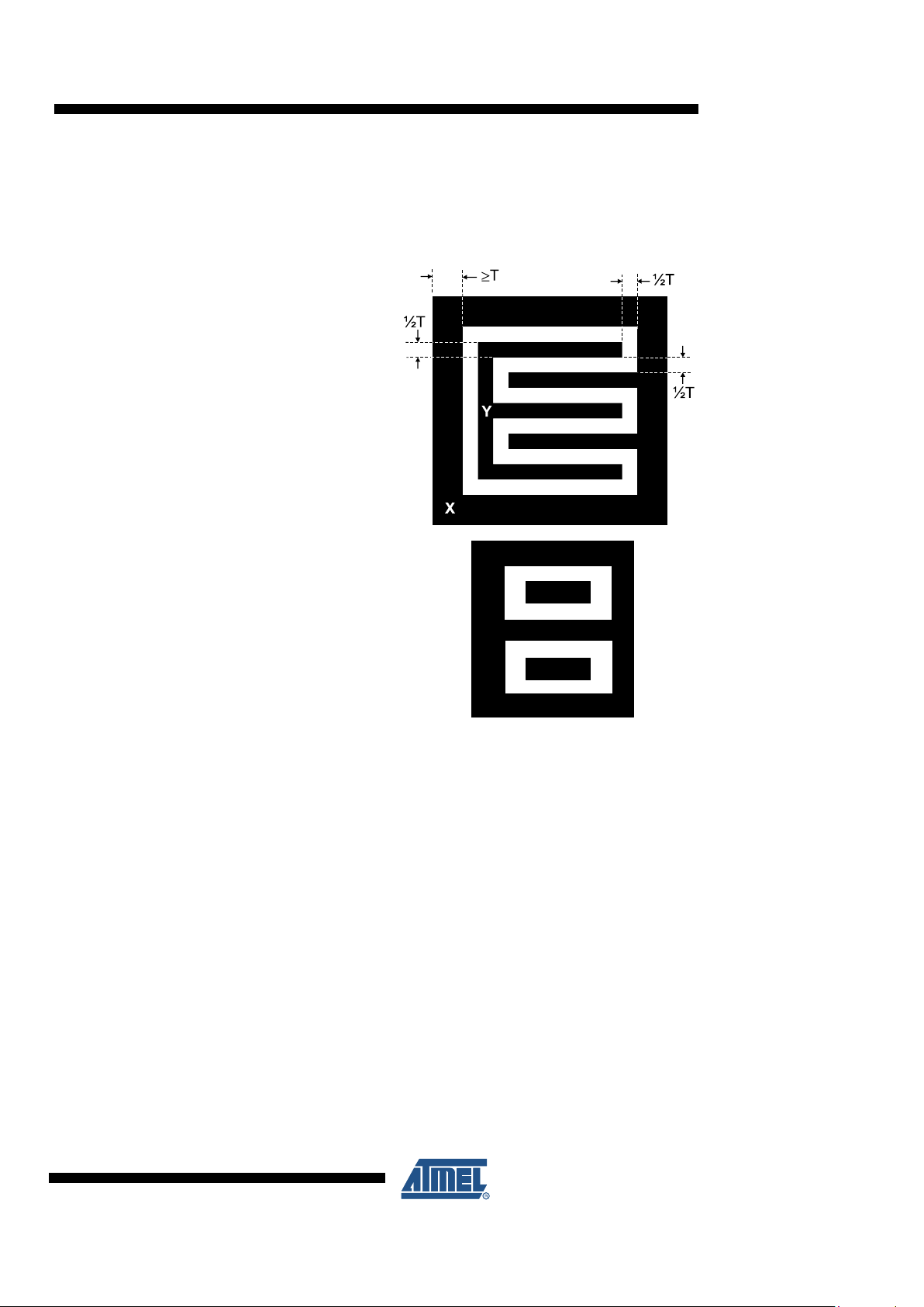
The internal pattern can be interdigitated as shown in Figure 4-6.
For small, dense keypads, electrodes such as shown in the lower half of Figure 4-6 can be used.
Where the panels are thin (under 2 mm thick) the electrode density can be quite high.
9
9502A–AT42–07/08
AT42QT2160
For better surface moisture suppression, the outer perimeter of X should be as wide as possible,
and there should be no ground planes near the keys. The variable “T" in this drawing represents
the total thickness of all materials that the keys must penetrate.
Figure 4-6. Recommended Key Structure
Note: “T" should ideally be similar to the complete thickness the fields need to penetrate to the touch
surface. Smaller dimensions will also work but will give less signal strength. If in doubt, make the
pattern coarser. The lower figure shows a simpler structure used for compact key layouts, for
example for mobile phones. A layout with a common X drive and two receive electrodes is
depicted
4.9 Setting the Slider
4.9.1 Introduction
Groups of keys can be configured as a slider, in addition to their use as keys. The slider uses the
Y0 line of the matrix and must start at X0, with the keys placed in consecutive numerical order.
The slider can take up a programmable number of keys on the Y0 line. The remaining keys on
that Y line behave as normal.
Positional data is calculated in a customizable range of 2 bits (0-3) to 8 bits (0-255). Geometric
constraints may mean that the data will not reach the full range. Thinner dielectric or the use of
more keys in a slider will increase the data range towards the ends.
Stability of the reported position will be dependent on the amount of signal on the slider keys.
Running at higher resolutions, with a thick panel might produce a fluctuating reported position.
Y1
Y0
X0

10
9502A–AT42–07/08
AT42QT2160
Key sizes should be in the 5-7mm range when used in the slider to get the best linearity. The
slider should be made up of however many of these elements are required to fit their
dimensions.
The slider will be treated as an object in the Adjacent Key Suppression (AKS) groupings. The
keys in the slider would normally be set to the same burst length and threshold, although
adjustments can be made in these at the expense of linearity.
4.9.2 AKS Technology and the Slider
There can be up to three AKS groups, implemented so that only one key in each group may be
reported as being touched at any one time. The AKS technique will lock onto the dominant key,
and until this key is released, other keys in the group will not be reported as in detection. This
allows a user to slide a finger across multiple keys with only the dominant key reporting touch.
Each key may be in one of the groups 1...3, or in group 0 meaning that it is not AKS enabled.
Keys in the slider are not able to use AKS technique against each other. This is necessary to
enable smooth scrolling. Multiple keys within the slider can be in detect at the same time,
regardless of the AKS settings. The AKS technique will, however, work against keys outside the
object or within another object. For example, if a slider is in the same AKS group as keys, then
touching anywhere on the slider will cause the AKS technique to suppress the keys. Similarly
touching the keys first will suppress the slider.
Note: For normal operation all keys in the slider should be placed in the same AKS group.
4.10 PCB Layout, Construction
4.10.1 Overview
It is best to place the chip near the touch keys on the same PCB so as to reduce X and Y trace
lengths, thereby reducing the chances for EMC problems. Long connection traces act as RF
antennae. The Y (receive) lines are much more susceptible to noise pickup than the X (drive)
lines.
Even more importantly, all signal related discrete parts (resistors and capacitors) should be very
close to the body of the chip. Wiring between the chip and the various resistors and capacitors
should be as short and direct as possible to suppress noise pickup.
Ground planes, if used, should be placed under or around the QT chip itself and the associated
resistors and capacitors in the circuit, under or around the power supply, and back to a
connector. Ground planes can be used to shield against radiated noise, but at the expense of a
reduction in sensitivity as described previously.
Note: When using ground planes/floods, parasitic capacitance on Y lines can lead to reduced charge-
transfer efficiency. For noise suppression, ground planes/floods can be beneficial around and
between keys on the touch side of the PCB. However, it is advisable to route Y lines on the PCB
layer furthest away from the plane/flood, to reduce parasitic capacitance. Cross-hatched ground
patterns can act as effective shields, while helping to reduce parasitic capacitance. Ground
planes/floods around the chip are generally acceptable, taking into account the same considerations as for the Y line parasitics.
4.10.2 LED Traces and Other Switching Signals
Digital switching signals near the Y lines will induce transients into the acquired signals,
deteriorating the SNR performance of the device. Such signals should be routed away from the
Y lines, or the design should be such that these lines are not switched during the course of
signal acquisition (bursts).
11
9502A–AT42–07/08
AT42QT2160
LED terminals which are multiplexed or switched into a floating state and which are within or
physically very near a key structure (even if on another nearby PCB) should be bypassed to
either Vss or Vdd with at least a 10nF capacitor to suppress capacitive coupling effects which
can induce false signal shifts. The bypass capacitor does not need to be next to the LED, in fact
it can be quite distant. The bypass capacitor is noncritical and can be of any type.
LED terminals which are constantly connected to Vss or Vdd do not need further bypassing.
4.10.3 Tracks
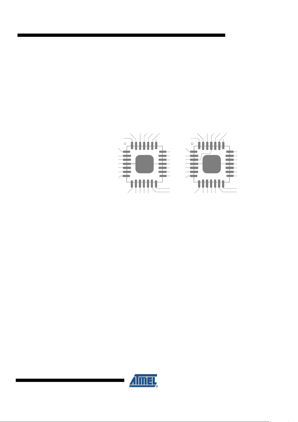
The central pad on the underside of the chip should be connected to ground. Do not run any
tracks underneath the body of the chip, only ground.
Figure 4-7. Position of Tracks
4.10.4 PCB Cleanliness
All capacitive sensors should be treated as highly sensitive circuits which can be influenced by
stray conductive leakage paths. QT devices have a basic resolution in the femtofarad range; in
this region, there is no such thing as “clean flux". Flux absorbs moisture and becomes
conductive between solder joints, causing signal drift and resultant false detections or transient
losses of sensitivity or instability. Conformal coatings will trap in existing amounts of moisture
which will then become highly temperature sensitive.
The designer should specify ultrasonic cleaning as part of the manufacturing process, and in
cases where a high level of humidity is anticipated, the use of conformal coatings after cleaning
to keep out moisture.
4.11 Power Supply Considerations
See Section 10.2 on page 43 for the Vdd range and short-term power supply fluctuations. If the
power supply fluctuates slowly with temperature, the device will track and compensate for these
changes automatically with only minor changes in sensitivity. If the supply voltage drifts or shifts
quickly, the drift compensation mechanism will not be able to keep up, causing sensitivity
anomalies or false detections.
As the device uses the power supply itself as an analog reference, the power should be very
clean and come from a separate regulator. A standard inexpensive Low Dropout (LDO) type
regulator should be used that is not also used to power other loads such as LEDs, relays, or
other high current devices. Load shifts on the output of the LDO can cause Vdd to fluctuate
enough to cause false detection or sensitivity shifts.
Example of g trackingood
Example of bad tracking

12
9502A–AT42–07/08
AT42QT2160
Caution: A regulator IC shared with other logic devices can result in erratic operation and is not
advised.
A regulator can be shared among two or more QT devices on one board. Refer to page 15 for
suggested regulator manufacturers.
A single ceramic 0.1uF bypass capacitor, with short traces, should be placed very close to
supply pins 3 and 4 of the IC. Failure to do so can result in device oscillation, high current
consumption, erratic operation etc. Pins 16 and 17 do not require bypassing if the traces
between these pins and power traces are short.
4.12 Startup/Calibration Times
The device requires initialization times of approximately 70ms. The CHANGE line will go low and
calibration will start (takes 15 matrix scans), after this start up period is over.
4.13 Calibration
Calibration does not occur periodically. Keys are only calibrated on power-up and when:
•Enabled
AND
– held in detect for too long. The negative recalibration delay (NRD) period is specified
by the user
OR
– the signal delta value is greater than the positive threshold value, defined as
reference value plus three-quarters of the negative threshold
OR
– the user issues a recalibrate command
An interrupt on the CHANGE
pin occurs when there is a change in the key status bytes. An
interrupt will occur on calibration only if at least one of the keys or objects was in detect as
recalibration will then cause a status change.
4.14 Reset Input
The RST pin can be used to reset the device to simulate a power-down cycle, in order to bring
the device up into a known state should communications with the device be lost. The pin is
active low, and a low pulse lasting at least 10µs must be applied to this pin to cause a reset.
If an external hardware reset is not used, the reset pin may be connected to Vdd.

13
9502A–AT42–07/08
AT42QT2160
4.15 Spread Spectrum Acquisitions
QT2160 uses spread-spectrum burst modulation. This has the effect of drastically reducing the
possibility of EMI effects on the sensor keys, while simultaneously spreading RF emissions. This
feature is hard-wired into the device and cannot be disabled or modified.
Spread spectrum is configured as a frequency chirp over a wide range of frequencies for robust
operation.
4.16 Detection Integrator
See also Section 4.2 on page 5.
The device features a detection integration mechanism, which acts to confirm a detection in a
robust fashion. A per-key counter is incremented each time the key has exceeded its threshold
and stayed there for a number of acquisitions. When this counter reaches a preset limit the key
is finally declared to be touched.
For example, if the limit value is 10, then the device has to exceed its threshold and stay there
for 10 acquisitions in succession without going below the threshold level, before the key is
declared to be touched. If on any acquisition the signal is not seen to exceed the threshold level,
the counter is cleared and the process has to start from the beginning.
4.17 Sleep
The device operates on a fixed 16ms cycle time basis. The device will perform a set of
measurements and then sleep for the rest of the cycle to conserve power.
There are two user-configurable sleep modes; Low Power (LP) mode and SLEEP mode.
The LP setting (see Section 4.2 on page 5) is used for conserving power when there are no
touches and is set to be a long time period. This will determine how often the device wakes up to
do drift compensation. It also determines the maximum response time to the first touch after
inactivity.
When a valid touch is registered, the device enters minimum cycle time (16ms) for a faster
response to key touch and object operation. The device will stay in this mode if it continues to
see keys being touched and released. There is a user-selectable inactivity timeout i.e. the
awake timeout.
The measurement period needs to be shorter than the 16ms fixed cycle time for optimum
operation. If the measurement time exceeds the 16ms fixed cycle time, a CYCLE OVERRUN bit
is set in the general status register. The QT2160 will still operate if the 16ms fixed cycle time is
exceeded, but the timing for the timed parameters, e.g. drift compensation negative recalibration
time out etc. will slightly change.
A low power setting of zero causes the device to enter an ultra-low power mode (SLEEP), where
no measurements are carried out. SLEEP mode also stops the internal watchdog timer, so that
the part is totally dormant, and current drain is <2µA. The PWM function will not be carried out
during SLEEP, therefore it is recommended driving the GPIOs/GPOs to known states before
entering SLEEP mode.
The QT2160 wakes from SLEEP mode if there is an address match on the
I2C-compatible bus, a
hardware reset on the RST
pin or an LP mode is set. If the Wake option is set for the dedicated
GPIO inputs, then the QT2160 will trigger the CHANGE
line if a change in status (either positive
or negative going edge) of the respective GPIO is detected, in SLEEP mode.

14
9502A–AT42–07/08
AT42QT2160
4.18 General Purpose Inputs/Outputs
There are three dedicated GPIOs (GPIO1...3) and eight GPOs shared with X lines (X0...7).
Shared GPOs are always outputs, whereas dedicated GPIOs can be set to be outputs or inputs.
GPIOs set to input can be used for reading dome switches or logic signals. Outputs can be used
to drive LEDs, or other devices. It is recommended driving external devices through the use of
bipolar transistors or MOSFETs, so as not to affect capacitive sensing if a load fluctuates the
power rail by drawing/sinking too much current.
All GPOs and GPIOs set to output can be PWM driven, if the corresponding PWM bit is set. Note
that the PWM duty cycle will be an approximation, as GPIOs will not be switched during
acquisition bursts.
The dedicated GPIOs have a Wake option, that if enabled will enable dedicated GPIOs set as
inputs, to be read in SLEEP mode.
Note that shared GPOs (X0...X7) are driven by the burst pulses during acquisition bursts, if the
corresponding X line is used in the keys/slider. A low pass filter can be inserted to eliminate
these burst pulses, as shown in Figure 4-9 on page 16.
15
9502A–AT42–07/08
AT42QT2160
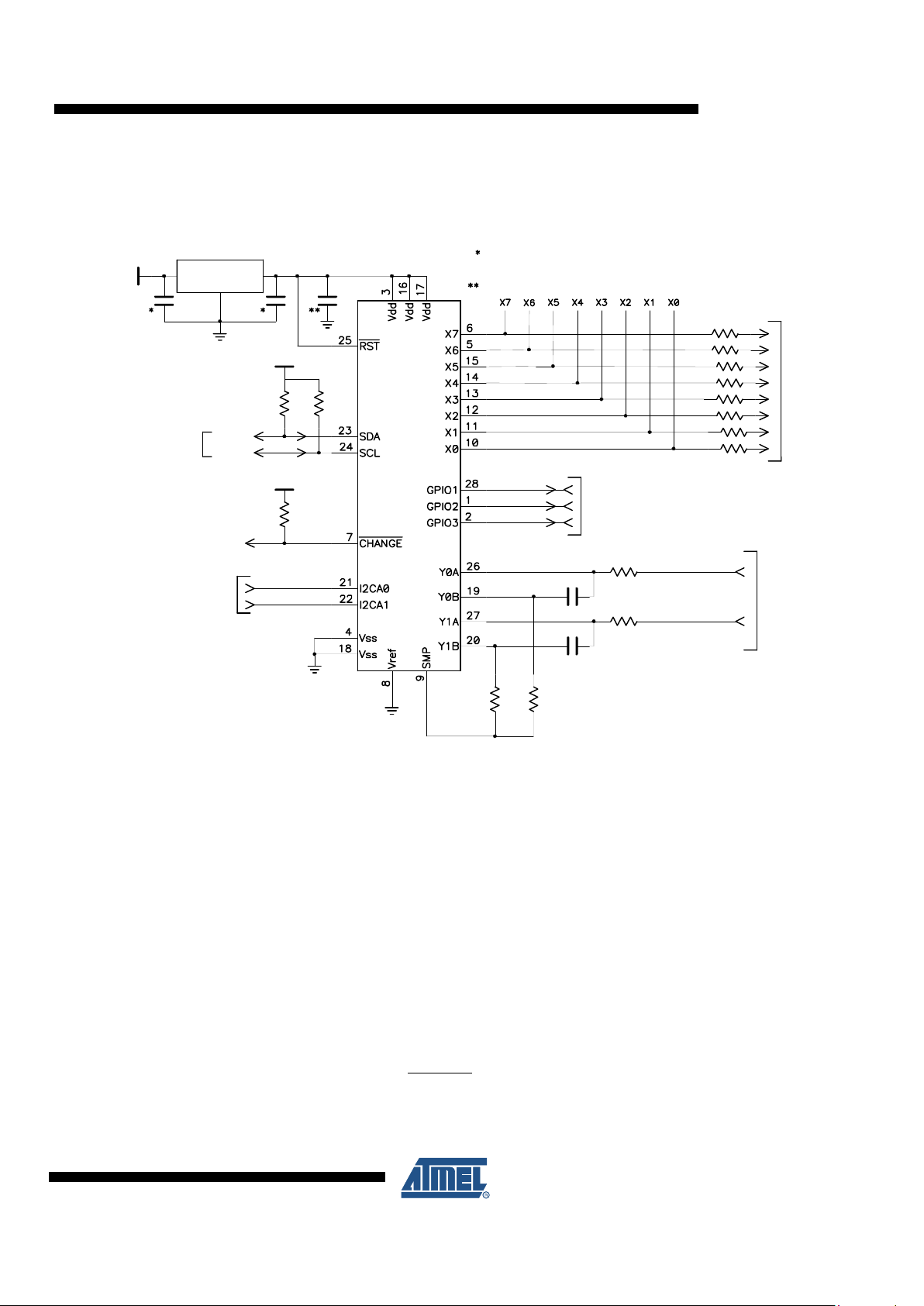
4.19 Wiring
Figure 4-8. Wiring Diagram
Suggested regulator manufacturers:
• Toko (XC6215 series)
• Seiko (S817 series)
• BCDSemi (AP2121 series)
Re Figure 4-8 check the following sections for component values:
• Section 4.3 on page 5: Cs capacitors (Cs0...Cs1)
• Section Note: on page 7: Sample resistors (Rs0...Rs1)
• Section 4.7 on page 7: Matrix resistors (Rx0...Rx7, Ry0...Ry1)
• Section 4.11 on page 11: Voltage levels
• Section 6.4 on page 22: SDA, SCL pull-up resistors (Rp)
• Section 4.2 on page 5: CHANGE
resistor (Rchg)
• Section 4.2 on page 5:
I2C-compatible addresses
Rp Rp
MATRIX Y SCAN IN
MATRIX X DRIVE
Rchg
VREG
Rx0
Rx3
Rx6
VDD
SCL
SDA
Rs1
Cs0
Cs1
Ry1
Rx2
Rx1
Rx7
Rx5
Vunreg
VDD
VDD
Ry0
Rx4
CHANGE
I2C
I2C ADDRESS
SELECT
QT2160
Rs0
General purpose
inputs/outp uts
Notes:
1) the central pad on the underside of the chip is a
Vss pin and should be connected to ground .
Do not put any other tracks underneath the body
of the chip.
2) it is important to place all Rx, Ry, Cs and Rs
components physically n ear to the chip .
3) leave YnA, YnB unconnected
if not used.
follow regu lator manuf acturers rec ommended values for input
and output bypass capacitors.
tightly wire a 100nF bypass capacitor between Vdd and Vss (pins 3 and 4).
 Loading...