

Page 1
Features
• Wake-up Function for a Microcontroller with Preamble Detection
• 1mV
• 1 µA Standby Current
• Power Supply: 2V to 3.8V
• Baud Rate: up to 4 kbps (ASK Modulation)
• Operation Temperature: up to 125°C
• Withstands +175°C
• Few External Components
Sensitivity
rms
Interface IC for
Application
• Tire Pressure Monitoring (TPM)
1. Description
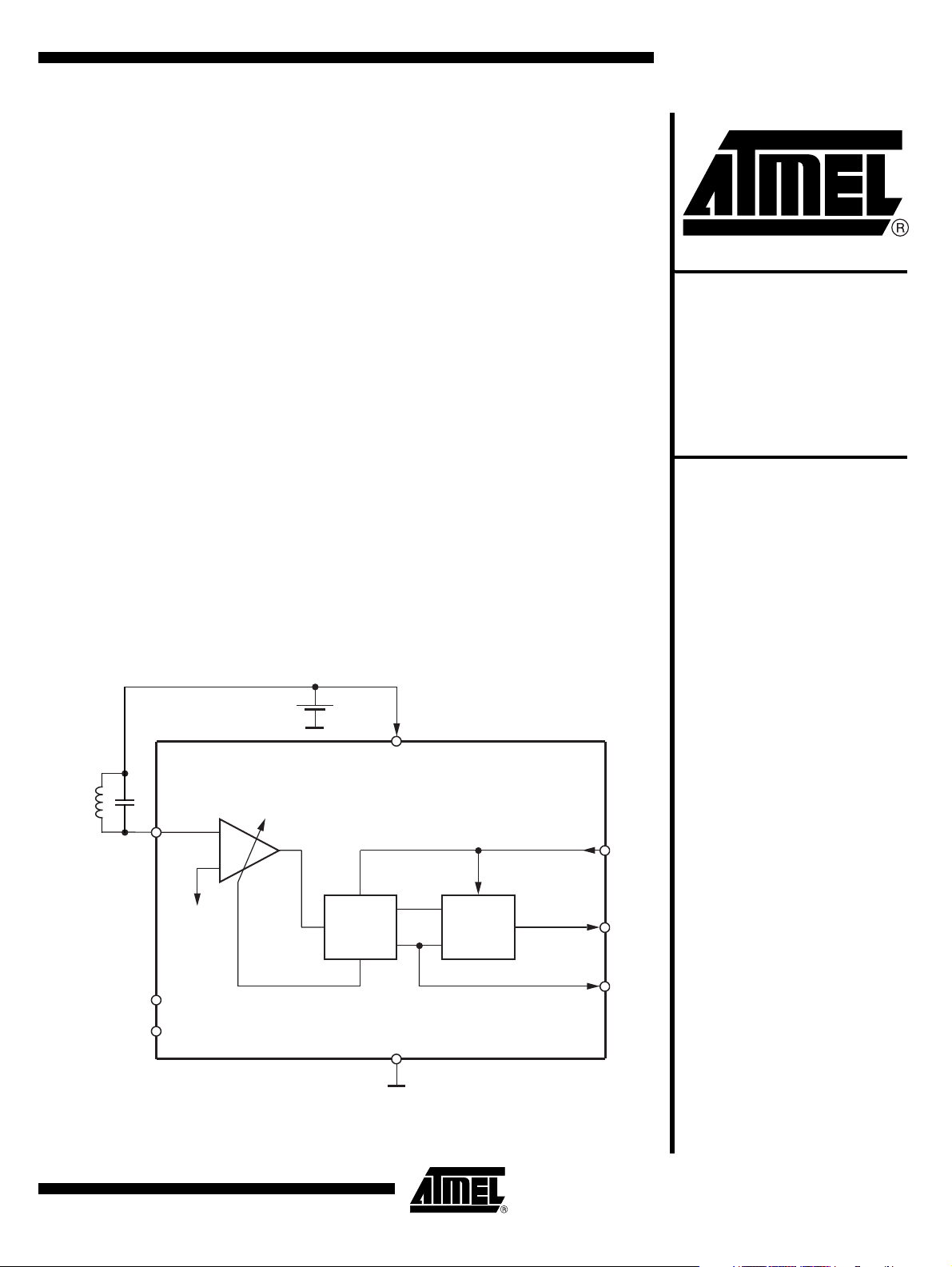
The ATA5283 is a 125 kHz ultra-low power receiver used for the wake-up function of
Tire Pressure Monitoring (TPM) application. The sensitive input stage of the IC amplifies and demodulates the carrier signal from the antenna coil to a digital output signal
for a microcontroller. During the standby mode the preamble detection unit monitors
the incoming signal and activates the wake-up output and the data output, if the IC
receives a proper 125 kHz carrier signal.
By combining the IC with an antenna coil, a microcontroller, an RF transmitter/transceiver, a battery, temperature- and pressure sensor, it is possible to design a
complete Tire Pressure Monitoring system (TPM).
Figure 1-1. Block Diagram
Battery
Lx
COIL
VDD
Amplifier
with AGC
ATA5283
RESET
125 kHz
Wake-up
Function
ATA5283
TST1
TST2
Vref
Condi-
tioner
GND
Preamble
check
N_WAKEUP
N_DATA
4598H–AUTO–03/07
Page 2
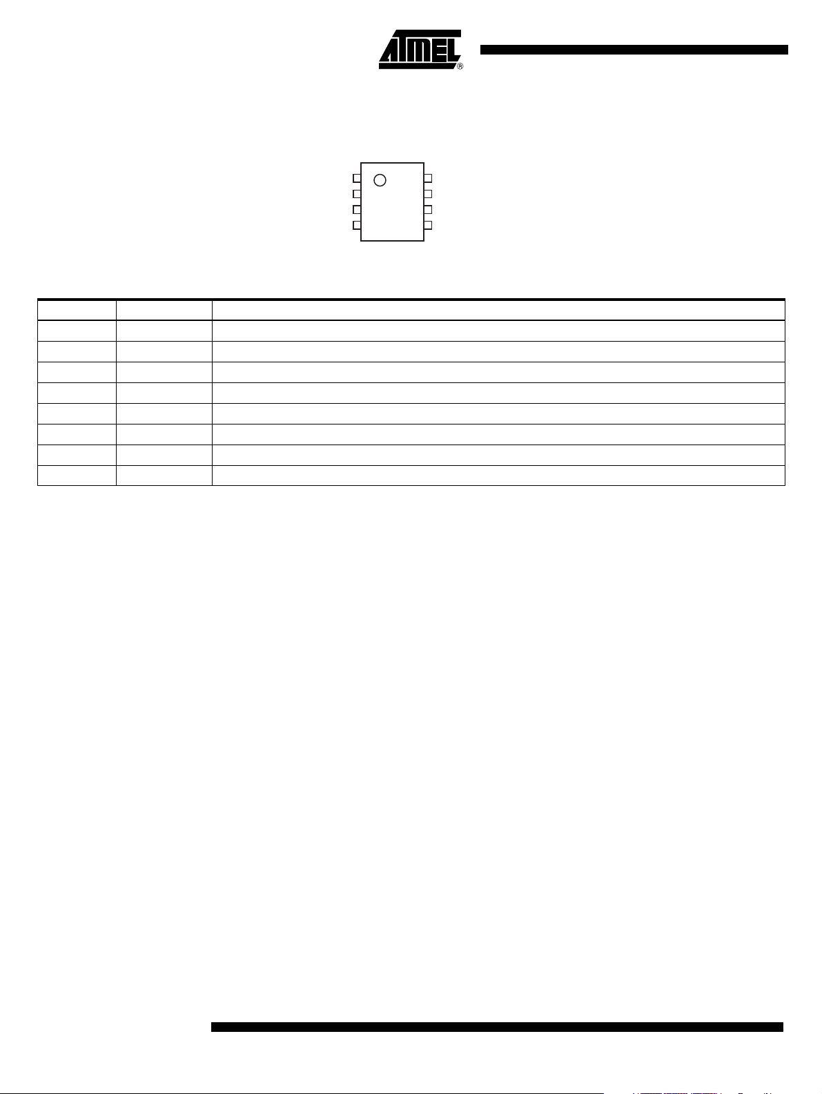
2. Pin Configuration
Figure 2-1. Pinning TSSOP8L
COIL 8
TST1
TST2
VSS
1
2
3
4
Figure 2-2. Pin Description
Pin Symbol Function
1 COIL Antenna coil input
2 TST1 Test pin (reserved)
3 TST2 Test pin (reserved)
4 VSS Signal ground
5 RESET External reset input
6 N_DATA Data signal
7 N_WAKEUP Low active wake-up signal for microcontroller
8 VDD Battery voltage
VDD
N_WAKEUP
7
N_DATA
6
RESET
5
2
ATA5283
4598H–AUTO–03/07
Page 3
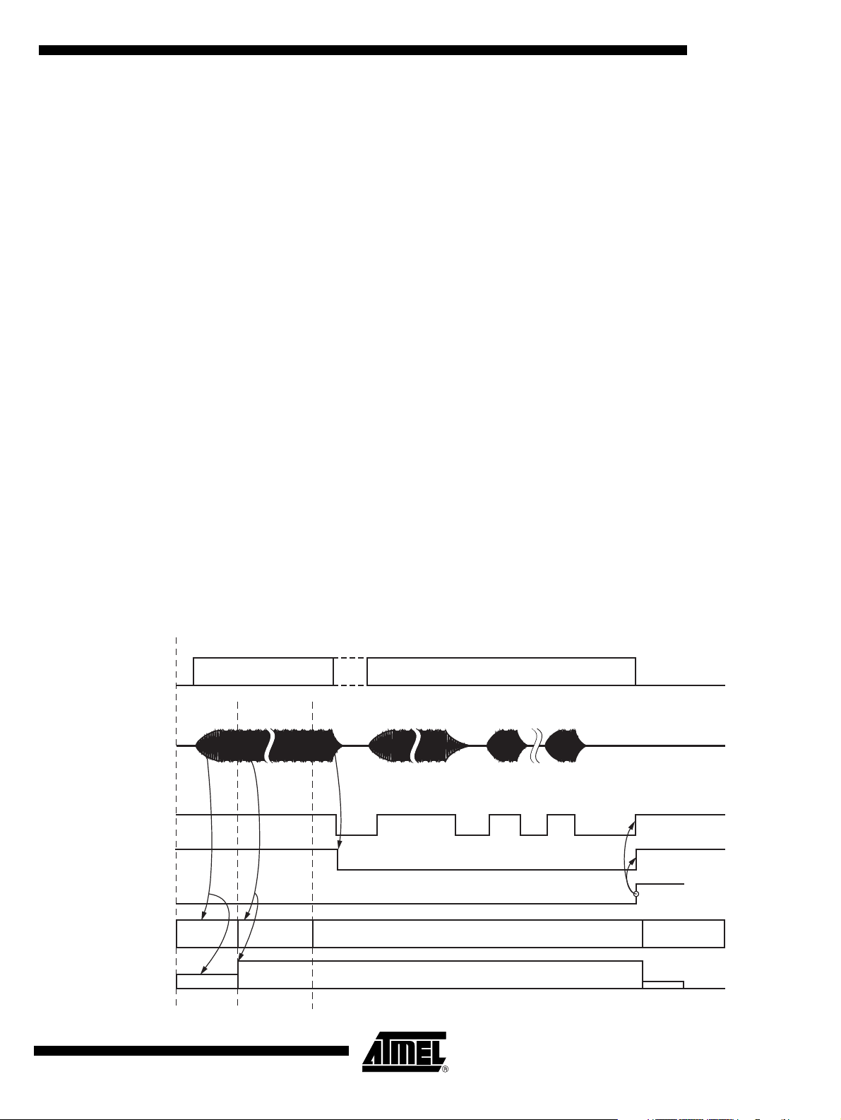
3. Functional Description
The ATA5283 is an ultra-low power ASK receiver. Without a carrier signal it operates in the
standby listen mode. In this mode it monitors the coil input with a very low current consumption.
To activate the IC and the connected control unit, the transmitting stage must send the preamble
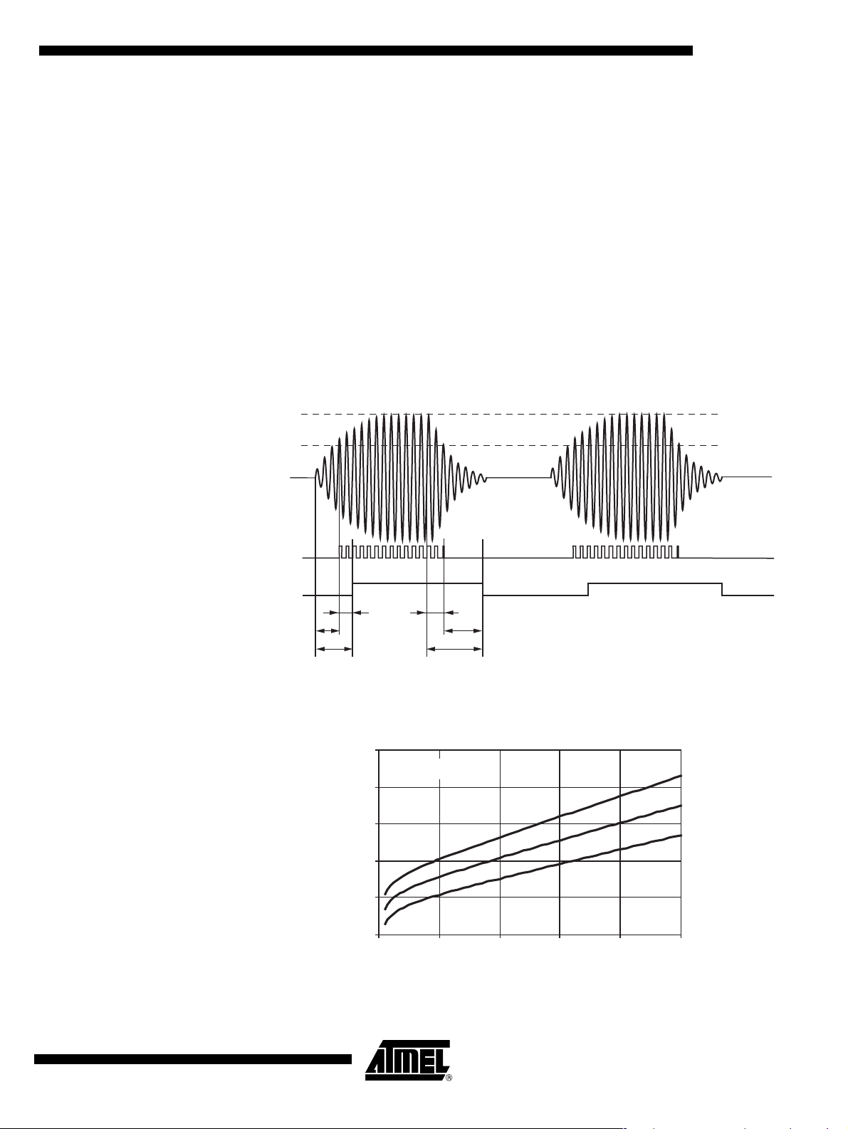
carrier burst. After a preamble is detected the IC is activated. It adapts the gain of the input stage
and enables the wake-up and the data output. The first gap at the end of the preamble generates a wake-up signal for the microcontroller. After that the receiver outputs the data signal at
N_DATA. To return the IC into the standby listen mode it must be reset via the RESET input.
3.1 AGC Amplifier
The input stage contains an Automatic Gain Control (AGC) amplifier to amplify the input signal
from the coil. The gain is adjusted by the automatic gain control circuit if a preamble signal is
detected. The high dynamic range of the AGC enables the IC to operate with input signals from
1mV
an amplitude adjusted for the following evaluation circuits’ preamble detection, signal conditioner, wake-up.
3.2 Preamble Detection
Before data transmission the IC stays in standby listen mode. To prevent the circuit from unintended operations in a noisy environment the preamble detection circuit checks the input signal.
A valid signal is detected by a counter after 192 carrier periods without interrupts. Short interrupts which are suppressed by the signal conditioner are tolerated. When a valid carrier
(preamble) is found the circuit starts the automatic gain control. It requires up to 512 carrier periods to settling. The complete preamble should have 704 carrier periods minimum. The preamble
is terminated and the data transfer is started with the first gap (Start Gap) in the carrier (see Fig-
ure 3-1).
to 1.1V
rms
ATA5283
. After the AGC settling time the amplifier output delivers a 125 kHz signal with
rms
Figure 3-1. Communication Protocol
Procedure
Signal
N_DATA
N_WAKEUP
RESET
Gain
control
Current
profile
192 Periods
of LF
No gain
control
1 µA
Preamble
> 5.64 ms
> 512 Periods
of LF
AGC
adjustment
Start
gap
Gain control
active
Data
0.5 µA2 µA
No gain
control
4598H–AUTO–03/07
3
Page 4
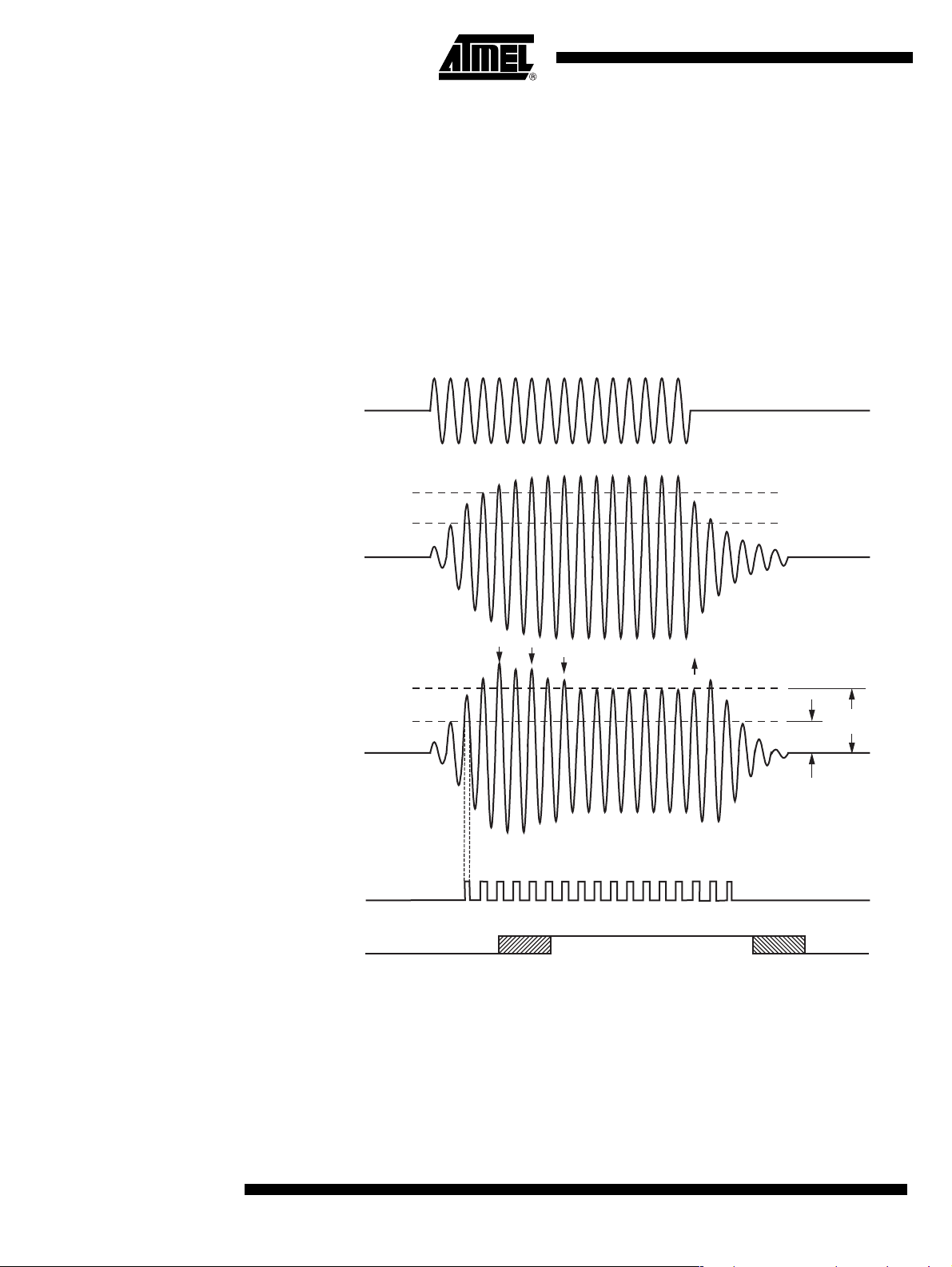
3.3 Automatic Gain Control
For a correct demodulation the signal conditioner needs appropriate internal signal amplitude.
To control the input signal the ATA5283 has a build in digital AGC. The gain control circuit regulates the internal signal amplitude to the reference value (Ref2, Figure 3-2). It decreases the
gain by one step if the internal signal exceeds the reference level for two periods and it
increases the gain by one step if eight periods do not achieve the reference level. In the standby
listen mode the gain is reset to the maximum value. If a valid preamble signal (192 valid carrier
clocks) is detected the automatic gain control is activated.
Note: With the variation of the gain the coil input impedance changes from high impedance to minimal
143 kΩ because of the internal regulator circuit (see Figure 3-8 on page 8).
Figure 3-2. Automatic Gain Control
Transmitted
signal
input
Coil
Gain control
reference
reference
Gain controlled
signal
Internal comparator
signal
N_DATA
Ref. 2
Ref. 1Gap detection
100%
50%
4
ATA5283
4598H–AUTO–03/07
Page 5
3.4 Signal Conditioner
The signal conditioner demodulates the amplifier output signal and converts it to a binary signal.
It compares the carrier signal with the 50% reference level (see Ref1 in Figure 3-3) and delivers
a logical 1, if the carrier signal stays below the reference and a logical 0, if it exceeds the reference level. A smoothing filter suppress the space between the half-waves as well as a few
missing periods in the carrier and glitches during the gaps.
The output signal of the signal conditioner is used as the internal data signal for the data output,
the wake-up logic and the preamble detection.
The timing of the demodulated data signal is delayed related to the signal at the transmitting
end. This delay is a function of the carrier frequency, the behavior of the smoothing filter and the
antenna Q-factor. The smoothing filter causes a delay of 3 to 6 periods (see t
3-3). The rest of the delay is caused by the build-up time of the antenna signal and is condi-
tioned on the Q-factor (see t
Figure 3-3. Output Timing
and tc in Figure 3-3).
a
ATA5283
and td in Figure
b
Ref.2
Ref.1
Coil
input
Comparator
output
N_DATA
t
b
t
a
t
ON
t
c
t
d
t
OFF
100%
50%
The following diagrams show the delay of the data signal as a function of the antenna Q-factor.
Figure 3-4. Turn On Delay Time (t
250
f
200
150
(µs)
on
t
100
50
field
) versus Antenna Q-Factor
ON
= 125 kHz
max.
min.
typ.
4598H–AUTO–03/07
0
05040302010
Q-factor
5
Page 6

3.5 Data Output
Figure 3-5. Turn Off Delay Time (t
200
180
160
140
120
100
(µs)
off
t
80
60
40
20
f
0
05040302010
) versus Antenna Q-Factor
off
= 125 kHz
field
max.
Q-factor
typ.
min.
The data output N_DATA outputs the demodulated and digitized LF signal according to the
envelope of the antenna input signal. In the standby mode the N_DATA output is disabled and
set to level 1. It is enabled by the wake-up signal and it outputs 1 level if the IC detects the carrier signal and a 0 level during the gaps (see Figure 3-1 on page 3).
As the circuit does not check the received data (except the preamble), it is up to the user to
choose the kind of encoding (pulse distance, Manchester, bi-phase...) wanted.
3.6 Wake-up Signal
3.7 Reset
The wake-up signal (N_WAKEUP) indicates that the ATA5283 has detected the end of a preamble signal and has left the standby mode. It can be used as a wake-up or a chip select signal for
an external device (see Figure 3-1 on page 3).
After a preamble is detected the first valid gap (Start Gap) sets the N_WAKEUP output to low
and enables the data output N_DATA. The N_WAKEUP holds the low level until the IC is reset
to the standby mode by a reset signal.
The IC is reset either by the internal POR circuit during a power on sequence or by a high pulse
at the RESET pin. After the reset all internal counters are in the initial state and the IC is in the
standby listen mode.
The POR circuit generates a reset while the supply voltage V
threshold V
and release the function of the IC if VDD exceeds this threshold.
POR
is below the power on reset
DD
A high signal at the RESET pin resets the complete circuit. If the IC is activated a reset signal is
necessary to activate the standby listen mode.
The RESET pin can also be used to hold the IC in a power down state. In this state the IC is out
of operation and the current consumption is below the standby current.
Note: The RESET pin is high impedance CMOS input. To avoid floating effects like undefined input
states and malfunctions it should not be open.
6
ATA5283
4598H–AUTO–03/07
Page 7

3.8 Standby Listen Mode
In the standby listen mode the IC monitors the coil input with a very low current consumption.
The automatic gain control is switched off and the gain is set to the maximum value. The
N_DATA and the N_WAKEUP output are set to a high level.
Before the controller enters its standby mode after the communication, it should activate the
standby listen mode of the ATA5283 with a reset signal. This measure ensures that the IC
enters the power saving standby mode and that the IC wakes the controller correctly with the
next preamble signal.
3.9 Applications
Figure 3-6 shows a typical TPM application of the ATA5283. Combined with the antenna reso-
nant circuit the ATA5283 is used as wake-up receiver for the microcontroller and the connected
temperature- and pressure-sensor.
Note: To avoid supply voltage ripples to affect the microcontroller, an RC filter (R1 = 100Ω, C1 = 10 nF)
Figure 3-6. Application
ATA5283
is recommended.
Central
board
controller
ATA5275
UHF Rx
T5743
Antenna
driver
125 kHz
433 kHz
LA
CA
1
2
3
Amplifier
with
AGC
Vref
UHF Tx
8
ATA5283
4
RESET
5
N_WAKEUP
7
N_DATA
6
C1
R1
Temp.
sensor
Micro
controller
Pressure
sensor
ATAR862
4598H–AUTO–03/07
7
Page 8

Figure 3-7. Pin Connection and Pin Protection
ATA5283
COIL_X
TST1
TST2
VSS
VDD
VDD
8
VDD
7
N_WAKEUP
N_DATA
6
RESET
5
1
Divider impedance
143 kΩ to 5 MΩ
VDD
2
2 kΩ
VDD
VDD
3
2 kΩ
VDD
4
1 kΩ
Figure 3-8. Coil Input Impedance
10000
max.
typ.
min.
1000
Z (kΩ)
100
1 100 1000 1000010
Coil Input Signal (mVpp)
8
ATA5283
4598H–AUTO–03/07
Page 9

ATA5283
4. Absolute Maximum Ratings
Stresses beyond those listed under “Absolute Maximum Ratings” may cause permanent damage to the device. This is a stress rating
only and functional operation of the device at these or any other conditions beyond those indicated in the operational sections of this
specification is not implied. Exposure to absolute maximum rating conditions for extended periods may affect device reliability.
Parameters Symbol Value Unit
Power supply V
Input voltage (except coil inputs) V
Input current coil I
Input voltage coil V
ESD protection (human body) V
Operating temperature range T
Withstanding 175°C t
Storage temperature range T
Soldering temperature T
DD
IN
CI
CI
ESD
amb
TEMP
stg
sld
5. Thermal Resistance
Parameters Symbol Value Unit
Thermal resistance junction ambient R
thJA
–0.3 to +6.5 V
VSS – 0.3 < V
IN
< V
+ 0.3 V
DD
±10 mA
VDD – 3.5 < VCI < V
+ 3.5 V
DD
4kV
–40 to +125 °C
30 min.
–40 to +150 °C
260 °C
210 K/W
6. Operating Range
Parameters Symbol Value Unit
Power supply range V
Operating temperature range T
DD
OP
2 to 3.8 V
–40 to +125 °C
4598H–AUTO–03/07
9
Page 10

7. Electrical Characteristics
VSS = 0V, VDD = 2V to 3.8V, T
No. Parameters Test Conditions Pin Symbol Min. Typ. Max. Unit Type*
1 Power Supply and Coil Limiter
1.1 Power supply 8 V
Reset supply current –40
Reset supply current +25 0.8 µA A
Reset supply current +85 0.8 µA C
1.2
Reset supply current +105 1.0 µA A
Reset supply current +125 1.5 µA C
Supply current
(standby listen mode) –40
Supply current
(standby listen mode) +25
Supply current
1.3
(standby listen mode) +85
Supply current
(standby listen mode) +105
Supply current
(standby listen mode) +125
Supply current with carrier
(AGC active) –40
Supply current with carrier
(AGC active) +25
Supply current with carrier
1.4
(AGC active) +85
Supply current with carrier
(AGC active) +105
Supply current with carrier
(AGC active) +125
Coil input voltage referred to
1.5
(Input coil limiter for
V
DD
channels X, Y, Z)
2 Amplifiers
2.1 Wake-up sensitivity 125 kHz input signal 7 V
2.2 Bandwidth Without coil 6 B
2.3 Upper corner frequency Without coil 6 f
2.4 Lower corner frequency Without coil 6 f
2.5 Input impedance f = 125 kHz 1 R
2.6 Input capacitance
*) Type means: A = 100% tested, B = 100% correlation tested, C = Characterized on samples, D = Design parameter
= –40°C to +105°C, characterized up to 125°C, unless other specified
amb
23.23.8 V A
143 kΩ A
= ± 1 mA
I
CI
= 2V
V
DD
= ± 1 mA
I
CI
VDD = 3.2V
I
= ± 1 mA
CI
= 3.8V
V
DD
≥ 1mV
V
IN
125 kHz
rms
at
DD
1, 2, 3,
8
1, 2, 3,
8
1,2, 3,
8
1-3 V
1C
I
DDR
I
DDL
I
DD
SENS
C
W
u
o
IN
IN
0.8 µA A
0.4
1.4 µA A
1.5 µA A
1.1
1.6 µA C
1.6 µA A
1.7 µA C
4.0 µA A
4.1 µA A
2
4.2 µA C
4.2 µA A
4.2 µA C
±1.4 Vp A
±1.6 Vp A
±1.8 Vp A
12.2mV
rms
150 kHz C
180 kHz C
30 kHz C
10 pF C
A
10
ATA5283
4598H–AUTO–03/07
Page 11

ATA5283
7. Electrical Characteristics (Continued)
VSS = 0V, VDD = 2V to 3.8V, T
No. Parameters Test Conditions Pin Symbol Min. Typ. Max. Unit Type*
3 Automatic Gain Control
3.1 Preamble detection time
3.2 AGC adjustment time
Signal change rate
3.3
(gap detection)
AGC correction time
3.4
(no gap detection)
3.5 Data rate (Q < 20) 125 kHz ASK DR 4 Kb/s A
3.6 Delay time RF signal to data 125 kHz ASK t
3.7 Delay time RF signal to data 125 kHz ASK t
4 Interface
4.1 Reset input level high 5 V
4.1.1 Reset pulse width V
4.2 Reset input level low 5 V
Reset input leakage current
4.3
low
Reset input leakage current
4.4
high
4.5 N_WAKEUP output level high I
4.6 N_WAKEUP output level low I
4.7 N_DATA output level high I
4.8 N_DATA output level low I
5 Power Supply and Reset
5.1 V
power on reset threshold V
DD
5.2 Power-up time
5.2.1
Standby reactivation delay
after pulse reset
RESET reactivation caused by
5.3
negative spikes on V
*) Type means: A = 100% tested, B = 100% correlation tested, C = Characterized on samples, D = Design parameter
= –40°C to +105°C, characterized up to 125°C, unless other specified
amb
VIN≥ 3mV
125 kHz
rms
at
t
DAGC
f = 125 kHz
V
DD
= 1 mV
IN
VIN = 3 mV
VIN = 30 mV
VIN = 100 mV
VIN = 1V
Coil input signal 100%
to 37% (τ)
Coil input signal:
50 to 100% changing
Coil input signal:
100 to 50% changing
RESET
V
RESET
V
RESET
NWAKEUP
NWAKEUP
N_DATA
N_DATA
Switch on V
rms
rms
rms
rms
rms
1t
1t
1t
= VDD 5t
= V
= V
SS
DD
5IIL-0.2 0 µA A
5IIH00.2µAA
= –100 µA 7 V
= 100 µA 7 V
= –100 µA 6 V
= 100 µA 6 V
to circuit
DD
active
f = 125 kHz T
t
= 500 ns 7 t
BDN
t
AGC
t
AGC
t
AGC
t
AGC
t
AGC
EOS
CORR
CORR
ON
OFF
HRESET
RESET
LRESET
HNWAKE
LNWAKE
HNDATA
LNDATA
POR
t
PON
Sbydel
RST
0.8 ×
V
DD
20 µs A
0
0.8 ×
V
DD
00.2 × V
0.8 ×
V
DD
00.2 × V
11.51.9 V A
10 200 µs C
192 Periods B
0
48
Periods C
220
292
450 512
20 Periods C
52 Periods C
208 Periods C
40 µs A
40 µs A
V
DD
0.2 ×
V
DD
V
DD
V
DD
VA
VC
VA
VA
DD
VA
VA
DD
100 ms C
800 µs C
4598H–AUTO–03/07
11
Page 12

8. Ordering Information
Extended Type Number Package Remarks
ATA5283P-6AQJ TSSOP8L 5000 pieces, taped and reeled, Pb-free
ATA5283P-6APJ TSSOP8L 500 pieces, taped and reeled, Pb-free
9. Package Information
Package: TSSOP 8L
Dimensions in mm
+0.05
1-0.15
0.85±0.05
0.31
0.65 nom.
3 x 0.65 = 1.95 nom.
Drawing-No.: 6.543-5083.01-4
Issue: 2; 15.03.04
+0.06
-0.07
3±0.1
85
14
0.1±0.05
3±0.1
3.8±0.3
4.9±0.1
technical drawings
according to DIN
specifications
-0.02
+0.05
0.15
12
ATA5283
4598H–AUTO–03/07
Page 13

10. Revision History
Please note that the following page numbers referred to in this section refer to the specific revision
mentioned, not to this document.
Revision No. History
4598H-AUTO-03/07 • Number 5.2.1 in section 7 “Electrical Characteristics” on page 11 added
4598G-AUTO-01/07
4598F-AUTO-09/05
ATA5283
• Put datasheet in a new template
• Pb-free logo on page 1 deleted
• Put datasheet in a new template
• Pb-free logo on page 1 added
• Heading Rows on Table “Absolute Maximum Ratings” on page 9 added
• Ordering Information on page 12 changed
4598H–AUTO–03/07
13
Page 14

Atmel Corporation Atmel Operations
2325 Orchard Parkway
San Jose, CA 95131, USA
Tel: 1(408) 441-0311
Fax: 1(408) 487-2600
Regional Headquarters
Europe
Atmel Sarl
Route des Arsenaux 41
Case Postale 80
CH-1705 Fribourg
Switzerland
Tel: (41) 26-426-5555
Fax: (41) 26-426-5500
Asia
Room 1219
Chinachem Golden Plaza
77 Mody Road Tsimshatsui
East Kowloon
Hong Kong
Tel: (852) 2721-9778
Fax: (852) 2722-1369
Japan
9F, Tonetsu Shinkawa Bldg.
1-24-8 Shinkawa
Chuo-ku, Tokyo 104-0033
Japan
Tel: (81) 3-3523-3551
Fax: (81) 3-3523-7581
Memory
2325 Orchard Parkway
San Jose, CA 95131, USA
Tel: 1(408) 441-0311
Fax: 1(408) 436-4314
Microcontrollers
2325 Orchard Parkway
San Jose, CA 95131, USA
Tel: 1(408) 441-0311
Fax: 1(408) 436-4314
La Chantrerie
BP 70602
44306 Nantes Cedex 3, France
Tel: (33) 2-40-18-18-18
Fax: (33) 2-40-18-19-60
ASIC/ASSP/Smart Cards
Zone Industrielle
13106 Rousset Cedex, France
Tel: (33) 4-42-53-60-00
Fax: (33) 4-42-53-60-01
1150 East Cheyenne Mtn. Blvd.
Colorado Springs, CO 80906, USA
Tel: 1(719) 576-3300
Fax: 1(719) 540-1759
Scottish Enterprise Technology Park
Maxwell Building
East Kilbride G75 0QR, Scotland
Tel: (44) 1355-803-000
Fax: (44) 1355-242-743
RF/Automotive
Theresienstrasse 2
Postfach 3535
74025 Heilbronn, Germany
Tel: (49) 71-31-67-0
Fax: (49) 71-31-67-2340
1150 East Cheyenne Mtn. Blvd.
Colorado Springs, CO 80906, USA
Tel: 1(719) 576-3300
Fax: 1(719) 540-1759
Biometrics
Avenue de Rochepleine
BP 123
38521 Saint-Egreve Cedex, France
Tel: (33) 4-76-58-47-50
Fax: (33) 4-76-58-47-60
Literature Requests
www.atmel.com/literature
Disclaimer: The information in this document is provided in connection with Atmel products. No license, express or implied, by estoppel or otherwise, to any
intellectual property right is granted by this document or in connection with the sale of Atmel products. EXCEPT AS SET FORTH IN ATMEL’S TERMS AND CONDI-
TIONS OF SALE LOCATED ON ATMEL’S WEB SITE, ATMEL ASSUMES NO LIABILITY WHATSOEVER AND DISCLAIMS ANY EXPRESS, IMPLIED OR STATUTORY
WARRANTY RELATING TO ITS PRODUCTS INCLUDING, BUT NOT LIMITED TO, THE IMPLIED WARRANTY OF MERCHANTABILITY, FITNESS FOR A PARTICULAR
PURPOSE, OR NON-INFRINGEMENT. IN NO EVENT SHALL ATMEL BE LIABLE FOR ANY DIRECT, INDIRECT, CONSEQUENTIAL, PUNITIVE, SPECIAL OR INCIDENTAL DAMAGES (INCLUDING, WITHOUT LIMITATION, DAMAGES FOR LOSS OF PROFITS, BUSINESS INTERRUPTION, OR LOSS OF INFORMATION) ARISING OUT
OF THE USE OR INABILITY TO USE THIS DOCUMENT, EVEN IF ATMEL HAS BEEN ADVISED OF THE POSSIBILITY OF SUCH DAMAGES. Atmel makes no
representations or warranties with respect to the accuracy or completeness of the contents of this document and reserves the right to make changes to specifications
and product descriptions at any time without notice. Atmel does not make any commitment to update the information contained herein. Unless specifically provided
otherwise, Atmel products are not suitable for, and shall not be used in, automotive applications. Atmel’s products are not intended, authorized, or warranted for use
as components in applications intended to support or sustain life.
© 2007 Atmel Corporation. All rights reserved. Atmel®, logo and combinations thereof, Everywhere You Are® and others are registered trade-
marks or trademarks of Atmel Corporation or its subsidiaries. Other terms and product names may be trademarks of others.
4598H–AUTO–03/07
 Loading...