


Features
• Minimal External Circuitry Requirements, No RF Components on the PC Board Except
Matching to the Receiver Antenna
• High Sensitivity, Especially at Low Data Rates
• Sensitivity Reduction Possible Even While Receiving
• Fully Integrated VCO
• Low Power Consumption Due to Configurable Self Polling with a Programmable Time
Frame Check
• Supply Voltage 4.5V to 5.5V
• Operating Temperature Range –40°C to +105°C
• Single-ended RF Input for Easy Adaptation to λ / 4 Antenna or Printed Antenna on PCB
• Low-cost Solution Due to High Integration Level
• ESD Protection According to MIL-STD. 883 (4 KV HBM) Except Pin POUT (2 KV HBM)
• High Image Frequency Suppression due to 1 MHz IF in Conjunction with a SAW
Front-end Filter
– Up to 40 dB is Thereby Achievable with Newer SAWs
• Programmable Output Port for Sensitivity Selection or for Controlling External
Periphery
• Communication to the Microcontroller Possible via a Single, Bi-directional Data Line
• Power Management (Polling) is also Possible by Means of a Separate Pin via the
Microcontroller
• 2 Different IF Bandwidth Versions are Available (300 kHz and 600 kHz)
UHF ASK
Receiver IC
ATA3741
1. Description
The ATA3741 is a multi-chip PLL receiver device supplied in an SO20 package. It has
been specially developed for the demands of RF low-cost data transmission systems
with low data rates from 1 kBaud to 10 kBaud (1 kBaud to 3.2 kBaud for FSK) in
Manchester or Bi-phase code. The receiver is well-suited to operate with Atmel's PLL
RF transmitter U2741B. Its main applications are in the areas of telemetering, security
technology, and keyless-entry systems. It can be used in the frequency receiving
range of f
ments made below refer to 433.92-MHz and 315-MHz applications.
= 300 MHz to 450 MHz for ASK or FSK data transmission. All the state-
0
4899B–RKE–10/06
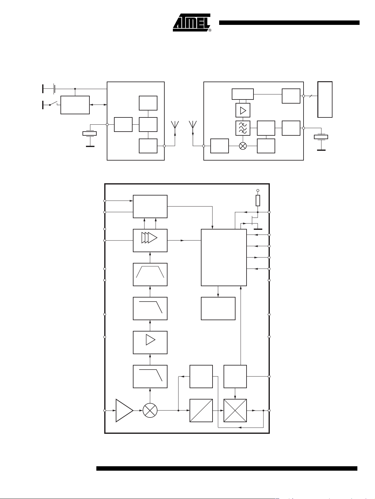
Figure 1-1. System Block Diagram
1 Li cell
Encoder
ATARx9x
Keys
Figure 1-2. Block Diagram
FSK/ASK
CDEM
AVCC
SENS
AGND
DGND
UHF ASK/FSK
Remote control transmitter
U2741B
PLL
XTO
VCO
Power
amp.
FSK/ASK
Demodulator
and data filter
RSSI
IF Amp
th
4
Order
Limiter out
Antenna
Antenna
DEMOD_OUT
Sensitivity
reduction
ATR3741
LNA
Polling circuit
and
control logic
FE CLK
UHF ASK/FSK
Remote control receiver
Demod
PLL
VCO
V
S
50 kΩ
DATA
ENABLE
TEST
POUT
MODE
DVCC
Control
1...3
Microcontroller
XTO
LPF
MIXVCC
LNAGND
LNA_IN
2
ATA3741
LNA
3 MHz
IF Amp
LPF
3 MHz
Standby logic
VCO
f
÷ 64
XTO
LFGND
LFVCC
XTO
LF
4899B–RKE–10/06
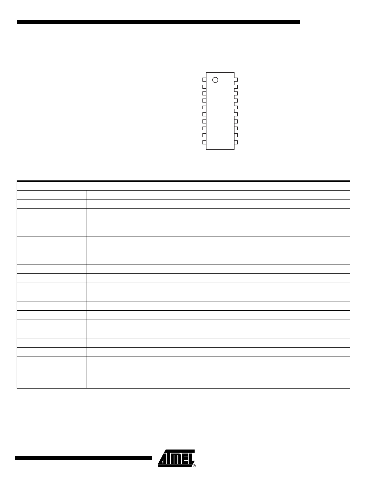
2. Pin Configuration
Figure 2-1. Pinning SO20
DATA
SENS
FSK/ASK
CDEM
AVCC
AGND
DGND
MIXVCC
LNAGND
LNA_IN
NC
1
2
3
4
5
6
7
8
9
10
Table 2-1. Pin Description
Pin Symbol Function
1 SENS Sensitivity-control resistor
2 FSK/ASK Selecting FSK/ASK. Low: FSK, High: ASK
3 CDEM Lower cut-off frequency data filter
4 AVCC Analog power supply
5 AGND Analog ground
6 DGND Digital ground
7 MIXVCC Power supply mixer
8 LNAGND High-frequency ground LNA and mixer
9 LNA_IN RF input
10 NC Not connected
11 LFVCC Power supply VCO
12 LF Loop filter
13 LFGND Ground VCO
14 XTO Crystal oscillator
15 DVCC Digital power supply
16 MODE Selecting 433.92 MHz/315 MHz. Low: 4.90625 MHz (USA). High: 6.76438 (Europe)
17 POUT Programmable output port
18 TEST Test pin, during operation at GND
Enables the polling mode
19 ENABLE
20 DATA Data output/configuration input
Low: polling mode off (sleep mode)
High: polling mode on (active mode)
20
19
18
17
16
15
14
13
12
11
ENABLE
TEST
POUT
MODE
DVCC
XTO
LFGND
LF
LFVCC
ATA3741
4899B–RKE–10/06
3
3. RF Front End
F
The RF front end of the receiver is a heterodyne configuration that converts the input signal into
a 1-MHz IF signal. As seen in the block diagram, the front end consists of an LNA (low noise
amplifier), LO (local oscillator), a mixer, and an RF amplifier.
The LO generates the carrier frequency for the mixer via a PLL synthesizer. The XTO (crystal
oscillator) generates the reference frequency f
erates the drive voltage frequency f
for the mixer. fLO is dependent on the voltage at pin LF. f
LO
is divided by a factor of 64. The divided frequency is compared to f
. The VCO (voltage-controlled oscillator) gen-
XTO
by the phase frequency
XTO
LO
detector. The current output of the phase frequency detector is connected to a passive loop filter
and thereby generates the control voltage V
is controlled in a way that fLO/ 64 is equal to f
for the VCO. By means of that configuration, V
LF
. If fLO is determined, f
XTO
can be calculated
XTO
LF
using the following formula:
f
LO
XTO
--------=
64
f
The XTO is a one-pin oscillator that operates at the series resonance of the quartz crystal. The
crystal should be connected to GND via a capacitor CL according to Figure 3-1. The value of the
capacitor is recommended by the crystal supplier. The value of CL should be optimized for the
individual board layout to achieve the exact value of f
and thereby of fLO. When designing the
XTO
system in terms of receiving bandwidth, the accuracy of the crystal and XTO must be
considered.
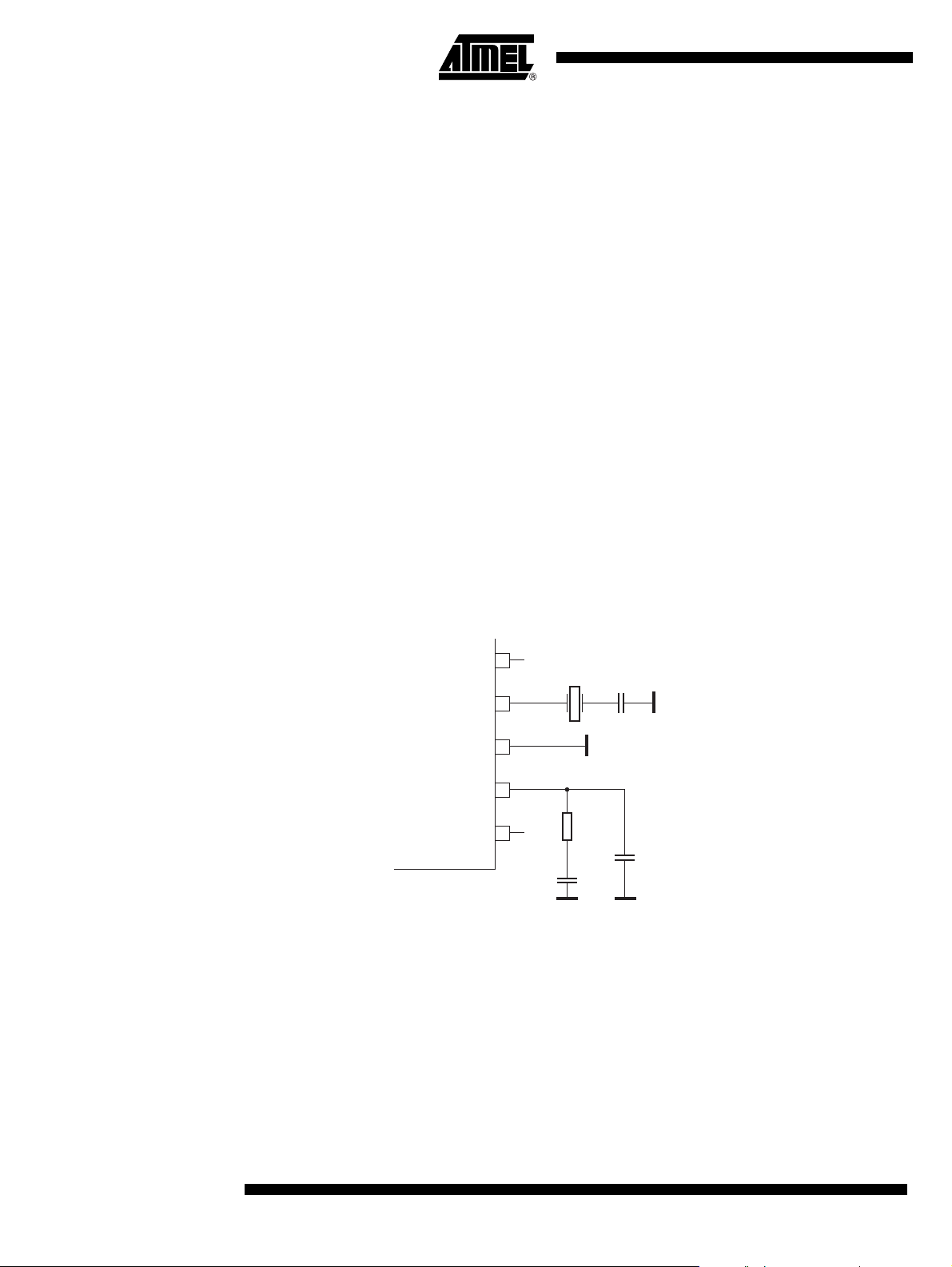
Figure 3-1. PLL Peripherals
V
DVCC
XTO
LFGND
S
C
L
R1 = 820Ω
C9 = 4.7 n
C10
C10 = 1 nF
= 100 kHz.
Loop
LF
V
LFVCC
S
R1
C9
The passive loop filter connected to pin LF is designed for a loop bandwidth of B
This value for B
exhibits the best possible noise performance of the LO. Figure 3-1 shows
Loop
the appropriate loop filter components to achieve the desired loop bandwidth. If the filter components are changed for any reason, please note that the maximum capacitive load at pin LF is
limited. If the capacitive load is exceeded, a bit check may no longer be possible since f
LO
cannot settle before the bit check starts to evaluate the incoming data stream. Therefore, self polling
also will not work .
4
ATA3741
4899B–RKE–10/06

ATA3741
fLO is determined by the RF input frequency fRF and the IF frequency fIF using the following formula:
f
LOfRFfIF
To determine f
frequency is f
is tuned by the crystal frequency f
f
LO
MODE 0 (USA) f
MODE 1 (Europe) f
The relation is designed to achieve the nominal IF frequency of f
tions. For applications where f
f
RF
f
is then dependent on the logical level at pin MODE and on fRF. Table 3-1 summarizes the dif-
IF
–=
, the construction of the IF filter must be considered at this point. The nominal IF
LO
= 1 MHz. To achieve a good accuracy of the filter’s corner frequencies, the filter
IF
. This means that there is a fixed relation between fIF and
XTO
that depends on the logic level at pin mode. This is described by the following formulas:
f
LO
----------==
IF
314
f
LO
------------------==
IF
432.92
= 1 MHz for most applica-
IF
= 315 MHz, MODE must be set to “0”. In the case of
RF
= 433.92 MHz, MODE must be set to ”1”. For other RF frequencies, fIF is not equal to 1 MHz.
ferent conditions.
The RF input either from an antenna or from a generator must be transformed to the RF input
pin LNA_IN. The input impedance of LNA_IN is specified in “Electrical Characteristics” on page
23. The parasitic board inductances and capacitances also influence the input matching. The RF
receiver ATA3741 exhibits its highest sensitivity at the best signal-to-noise ratio in the LNA.
Hence, noise matching is the best choice for designing the transformation network.
A good practice when designing the network is to start with power matching. From that starting
point, the values of the components can be varied to some extent to achieve the best sensitivity.
If a SAW is implemented into the input network, a mirror frequency suppression of ∆P
can be achieved. There are SAWs available that exhibit a notch at ∆f=2MHz. These SAWs
work best for an intermediate frequency of IF = 1 MHz. The selectivity of the receiver is also
improved by using a SAW. In typical automotive applications, a SAW is used.
Figure 3-2 on page 6 shows a typical input matching network for f
f
= 433.92 MHz using a SAW. Figure 3-3 on page 6 illustrates an input matching to 50Ω with-
RF
out a SAW. The input matching networks shown in Figure 3-3 are the reference networks for the
parameters given in the “Electrical Characteristics” on page 23.
Table 3-1. Calculation of LO and IF Frequency
Conditions Local Oscillator Frequency Intermediate Frequency
= 315 MHz, MODE = 0 fLO = 314 MHz fIF = 1 MHz
f
RF
= 433.92 MHz, MODE = 1 fLO = 432.92 MHz fIF = 1 MHz
f
RF
f
300 MHz < f
365 MHz < f
< 365 MHz, MODE = 0
RF
< 450 MHz, MODE = 1
RF
LO
f
LO
1
----------------------------=
1
1
----------+
314
f
RF
1
------------------+
432.92
f
IF
RF
-------------------=
f
f
IF
f
LO
----------=
314
f
LO
------------------=
432.92
Ref
= 315 MHz and
RF
=40dB
4899B–RKE–10/06
5
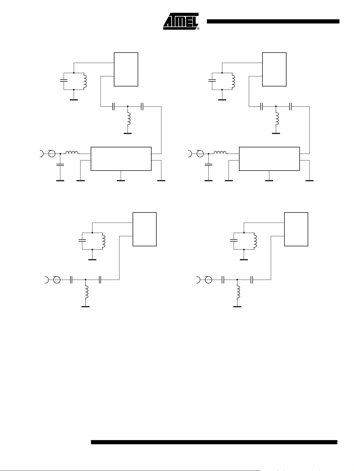
Figure 3-2. Input Matching Network With SAW Filter
8
LNAGND
ATA3741
9
C3
22p
fRF = 433.92 MHz
L2
IN
C2
8.2 pF
TOKO LL2012
F33NJ
33n
RF
1
2
25n
L
IN
IN_GND
LNA_IN
C16
100p
B3555
CASE_GND
3, 4 7, 8
L3
27n
C17
8.2p
TOKO LL2012
27NJ
OUT
OUT_GND
5
6
Figure 3-3. Input Matching Network Without SAW Filter
fRF = 433.92 MHz
15p
25n
8
9
LNAGND
ATA3741
LNA_IN
C3
47p
fRF = 315 MHz
IN
C2
10 pF
TOKO LL2012
RF
fRF = 315 MHz
L2
F82NJ
82n
33p
1
2
25n
L
IN
IN_GND
8
LNAGND
ATA3741
9
LNA_IN
C16
100p
B3551
CASE_GND
3, 4 7, 8
25n
L3
47n
C17
22p
TOKO LL2012
F47NJ
OUT
OUT_GND
8
LNAGND
ATA3741
9
LNA_IN
5
6
RF
IN
3.3p
22n
100p
TOKO LL2012
F22NJ
RF
IN
3.3p
39n
100p
TOKO LL2012
F39NJ
Please note that for all coupling conditions (Figure 3-2 and Figure 3-3), the bond wire inductivity
of the LNA ground is compensated. C3 forms a series resonance circuit together with the bond
wire. L = 25 nH is a feed inductor to establish a DC path. Its value is not critical but must be large
enough not to detune the series resonance circuit. For cost reduction, this inductor can be easily
printed on the PCB. This configuration improves the sensitivity of the receiver by about 1 dB to
2dB.
6
ATA3741
4899B–RKE–10/06

4. Analog Signal Processing
4.1 IF Amplifier
The signals coming from the RF front end are filtered by the fully integrated 4th-order IF filter.
The IF center frequency is f
is used. For other RF input frequencies, refer to Table 3-1 on page 5 to determine the center
frequency.
The ATA3741 is available with 2 different IF bandwidths. ATA3741-M2, the version with
B
= 300 kHz, is well suited for ASK systems where Atmel’s PLL transmitter U2741B is used.
IF
The receiver ATA3741-M3 employs an IF bandwidth of B
together with the U2741B in FSK and ASK mode. If used in ASK applications, it allows higher
tolerances for the receiver and PLL transmitter crystals. SAW transmitters exhibit much higher
transmit frequency tolerances compared to PLL transmitters. Generally, it is necessary to use
B
= 600 kHz together with such transmitters.
IF
4.2 RSSI Amplifier
The subsequent RSSI amplifier enhances the output signal of the IF amplifier before it is fed into
the demodulator. The dynamic range of this amplifier is DR
operated within its linear range, the best signal-to-noise ratio (SNR) is maintained in ASK mode.
If the dynamic range is exceeded by the transmitter signal, the SNR is defined by the ratio of the
maximum RSSI output voltage and the RSSI output voltage due to a disturber. The dynamic
range of the RSSI amplifier is exceeded if the RF input signal is about 60 dB higher compared to
the RF input signal at full sensitivity.
ATA3741
= 1 MHz for applications where fRF= 315 MHz or fRF=433.92MHz
IF
= 600 kHz. This version can be used
IF
= 60 dB. If the RSSI amplifier is
RSSI
In FSK mode, the SNR is not affected by the dynamic range of the RSSI amplifier.
The output voltage of the RSSI amplifier is internally compared to a threshold voltage V
V
is determined by the value of the external resistor R
Th_red
Sense
. R
is connected between
Sense
Th_red
pin SENS and GND or VS. The output of the comparator is fed into the digital control logic. This
makes it possible to operate the receiver at lower sensitivity.
If R
is defined by the value of R
is connected to VS, the receiver operates at a lower sensitivity. The reduced sensitivity
Sense
, the maximum sensitivity by the SNR of the LNA input. The
Sense
reduced sensitivity is dependent on the signal strength at the output of the RSSI amplifier.
Since different RF input networks may exhibit slightly different values for the LNA gain, the sensitivity values given in the electrical characteristics refer to a specific input matching. This
matching is illustrated in Figure 3-3 on page 6 and exhibits the best possible sensitivity.
R
can be connected to VS or GND via a microcontroller or by the digital output port POUT of
Sense
the ATA3741 receiver IC. The receiver can be switched from full sensitivity to reduced sensitivity
or vice versa at any time. In polling mode, the receiver will not wake up if the RF input signal
does not exceed the selected sensitivity. If the receiver is already active, the data stream at pin
DATA will disappear when the input signal is lower than defined by the reduced sensitivity.
Instead of the data stream, the pattern shown in Figure 4-1 is issued at pin DATA to indicate that
the receiver is still active.
Figure 4-1. Steady L State Limited DATA Output Pattern
.
4899B–RKE–10/06
DATA
t
min2
t
DATA_L_max
7

4.3 FSK/ASK Demodulator and Data Filter
The signal coming from the RSSI amplifier is converted into the raw data signal by the ASK/FSK
demodulator. The operating mode of the demodulator is set via pin ASK/FSK. Logic “L” sets the
demodulator to FSK, Logic “H” sets it into ASK mode.
In ASK mode an automatic threshold control circuit (ATC) is employed to set the detection reference voltage to a value where a good SNR is achieved. This circuit also implies the effective
suppression of any kind of in-band noise signals or competing transmitters. If the SNR exceeds
10 dB, the data signal can be detected properly.
The FSK demodulator is intended to be used for an FSK deviation of ∆f ≥ 20 kHz. Lower values
may be used, but the sensitivity of the receiver will be reduced. The minimum usable deviation is
dependent on the selected baud rate. In FSK mode, only BR_Range0 and BR_Range1 are
available. In FSK mode, the data signal can be detected if the SNR exceeds 2 dB.
The output signal of the demodulator is filtered by the data filter before it is fed into the digital
signal processing circuit. The data filter improves the SNR as its bandpass can be adopted to
the characteristics of the data signal. The data filter consists of a 1st-order high-pass filter and a
1st-order low-pass filter.
The high-pass filter cut-off frequency is defined by an external capacitor connected to pin
CDEM. The cut-off frequency of the high-pass filter is defined by the following formula:
f
cu_DF
-------------------------------------------------------------=
2 π× 30 kΩ× CDEM×
In self-polling mode, the data filter must settle very rapidly to achieve a low current consumption.
Therefore, CDEM cannot be increased to very high values if self-polling is used. On the other
hand, CDEM must be large enough to meet the data filter requirements according to the data
signal. Recommended values for CDEM are given in the “Electrical Characteristics” on page 23.
The values are slightly different for ASK and FSK mode.
The cut-off frequency of the low-pass filter is defined by the selected baud rate range
(BR_Range). BR_Range is defined in the OPMODE register (Section “Configuration of the
Receiver” on page 17). BR_Range must be set in accordance to the used baud rate.
The ATA3741 is designed to operate with data coding where the DC level of the data signal is
50%. This is valid for Manchester and Bi-phase coding. If other modulation schemes are used,
the DC level should always remain within the range of VDC_min = 33% and VDC_max = 66%.
The sensitivity may be reduced by up to 1.5 dB in that condition.
Each BR_Range is also defined by a minimum and a maximum edge-to-edge time (t
These limits are defined in the “Electrical Characteristics” on page 23. They should not be
exceeded to maintain full sensitivity of the receiver.
4.4 Receiving Characteristics
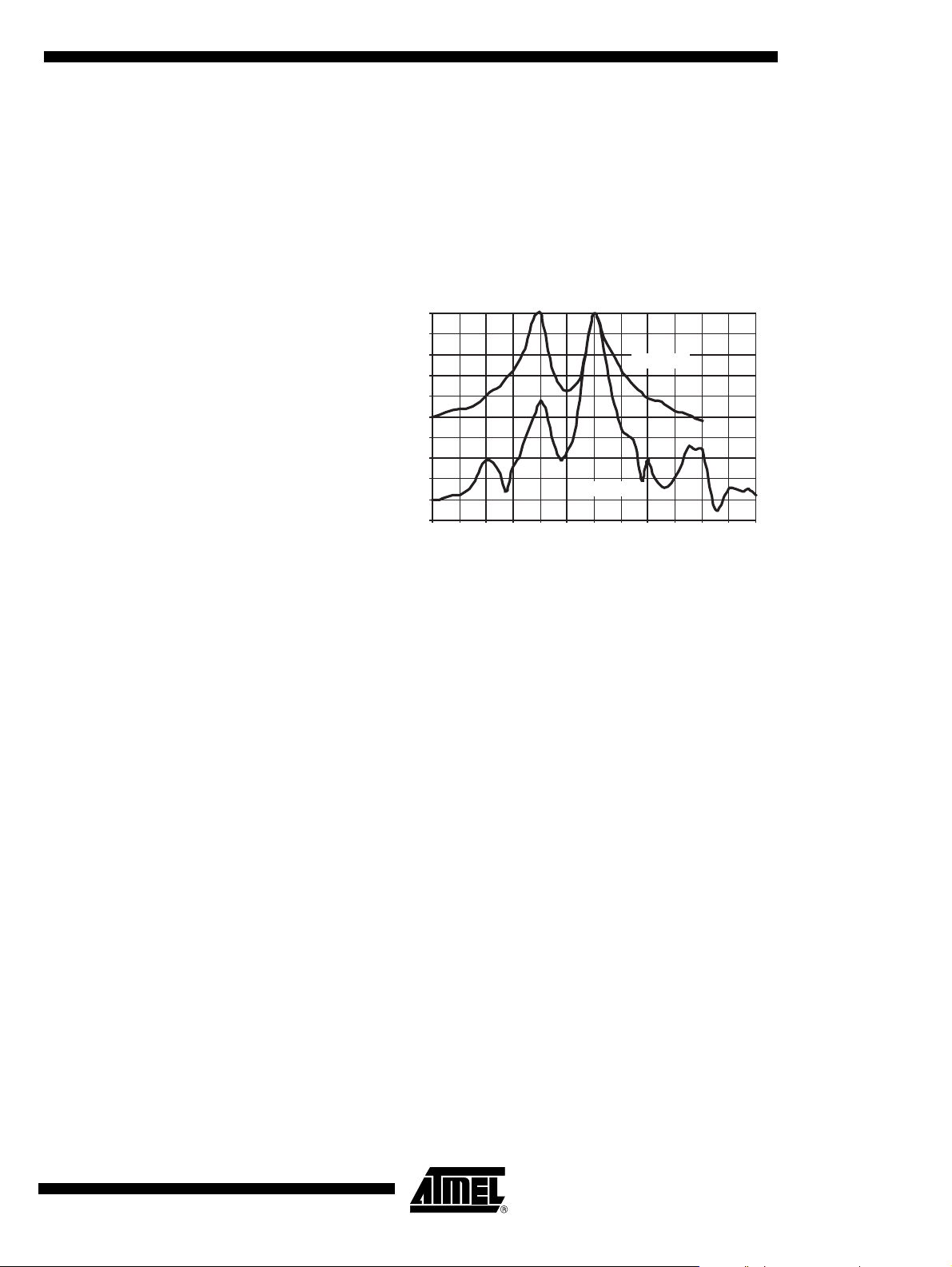
The RF receiver ATA3741 can be operated with and without a SAW front-end filter. In a typical
automotive application, a SAW filter is used to achieve better selectivity. The selectivity with and
without a SAW front-end filter is illustrated in Figure 4-2 on page 9. This example relates to ASK
mode and the 300-kHz bandwidth version of the ATA3741. FSK mode and the 600-kHz version
of the receiver exhibit similar behavior. Note that the mirror frequency is reduced by 40 dB. The
plots are printed relative to the maximum sensitivity. If a SAW filter is used, an insertion loss of
about 4 dB must be considered.
1
).
ee_sig
8
ATA3741
4899B–RKE–10/06
ATA3741
When designing the system in terms of receiving bandwidth, the LO deviation must be considered as it also determines the IF center frequency. The total LO deviation is calculated to be the
sum of the deviation of the crystal and the XTO deviation of the ATA3741. Low-cost crystals are
specified to be within ±100 ppm. The XTO deviation of the ATA3741 is an additional deviation
due to the XTO circuit. This deviation is specified to be ±30 ppm. If a crystal of ±100 ppm is
used, the total deviation is ±130 ppm in that case. Note that the receiving bandwidth and the
IF-filter bandwidth are equivalent in ASK mode but not in FSK mode.
Figure 4-2. Receiving Frequency Response
0.0
-10.0
-20.0
-30.0
-40.0
-50.0
-60.0
dP (dB)
-70.0
-80.0
-90.0
-100.0
-6.0 -5.0 -4.0 -3.0 -2.0 -1.0 0.0 1.0 2.0 3.0 4.0 5.0 6.0
df (MHz)
without SAW
with SAW
5. Polling Circuit and Control Logic
The receiver is designed to consume less than 1 mA while being sensitive to signals from a corresponding transmitter. This is achieved via the polling circuit. This circuit enables the signal
path periodically for a short time. During this time the bit-check logic verifies the presence of a
valid transmitter signal. Only if a valid signal is detected does the receiver remain active and
transfer the data to the connected microcontroller. If there is no valid signal present, the receiver
is in sleep mode most of the time, resulting in low current consumption. This condition is called
polling mode. A connected microcontroller is disabled during that time.
All relevant parameters of the polling logic can be configured by the connected microcontroller.
This flexibility enables the user to meet the specifications in terms of current consumption, system response time, data rate, etc.
Regarding the number of connection wires to the microcontroller, the receiver is very flexible. It
can be either operated by a single bi-directional line to save ports to the connected microcontroller, or it can be operated by up to three uni-directional ports.
5.1 Basic Clock Cycle of the Digital Circuitry
The complete timing of the digital circuitry and the analog filtering is derived from one clock. As
seen in Figure 5-1 on page 10, this clock cycle T
combination with a divider. The division factor is controlled by the logical state at pin MODE. The
frequency of the crystal oscillator (f
defines the operating frequency of the local oscillator (f
is derived from the crystal oscillator (XTO) in
Clk
) is defined by the RF input signal (f
XTO
) (See “RF Front End” on page 4).
LO
) which also
RFin
4899B–RKE–10/06
9
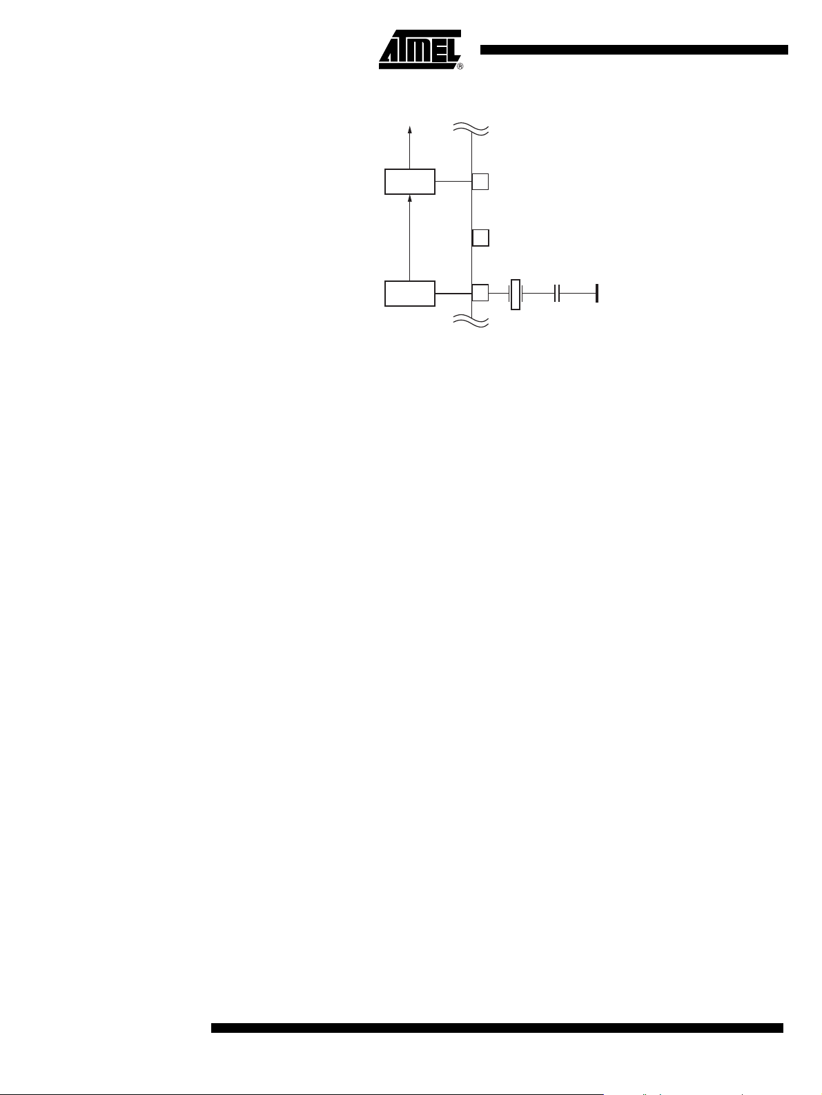
Figure 5-1. Generation of the Basic Clock Cycle
T
Divider
:14/:10
XTO
Clk
f
XTO
MODE
16
DVCC
15
XTO
14
L : USA (:10)
H: Europe (:14)
Pin MODE can now be set in accordance with the desired clock cycle T
Clk
. T
controls the fol-
Clk
lowing application-relevant parameters:
• Timing of the polling circuit including bit check
• Timing of analog and digital signal processing
• Timing of register programming
• Frequency of the reset marker
• IF filter center frequency (f
Most applications are dominated by two transmission frequencies: f
used in the USA, f
= 433.92 MHz in Europe. In order to ease the usage of all T
Send
IF0
)
= 315 MHz is mainly
Send
-dependent
Clk
parameters, the electrical characteristics display three conditions for each parameter.
• USA Applications
(f
= 4.90625 MHz, MODE = 0, T
XTO
= 2.0383 µs)
Clk
• Europe Applications
(f
= 6.76438 MHz, MODE = 1, T
XTO
= 2.0697 µs)
Clk
• Other applications
(T
is dependent on f
Clk
is given as a function of T
and on the logical state of pin MODE. The electrical characteristic
XTO
).
Clk
The clock cycle of some function blocks depends on the selected baud rate range (BR_Range)
which is defined in the OPMODE register. This clock cycle T
is defined by the following for-
XClk
mulas for further reference:
10
ATA3741
BR_Range = BR_Range0: T
BR_Range1: T
BR_Range2: T
BR_Range3: T
XClk
XClk
XClk
XClk
= 8 × T
= 4 × T
= 2 × T
= 1 × T
Clk
Clk
Clk
Clk
4899B–RKE–10/06
 Loading...